EP1679780B1 - DC/DC converter with current limit protection - Google Patents
DC/DC converter with current limit protection Download PDFInfo
- Publication number
- EP1679780B1 EP1679780B1 EP06250081.4A EP06250081A EP1679780B1 EP 1679780 B1 EP1679780 B1 EP 1679780B1 EP 06250081 A EP06250081 A EP 06250081A EP 1679780 B1 EP1679780 B1 EP 1679780B1
- Authority
- EP
- European Patent Office
- Prior art keywords
- switch
- current
- state
- circuit
- voltage
- Prior art date
- Legal status (The legal status is an assumption and is not a legal conclusion. Google has not performed a legal analysis and makes no representation as to the accuracy of the status listed.)
- Expired - Lifetime
Links
Images

Classifications
-
- H—ELECTRICITY
- H02—GENERATION; CONVERSION OR DISTRIBUTION OF ELECTRIC POWER
- H02M—APPARATUS FOR CONVERSION BETWEEN AC AND AC, BETWEEN AC AND DC, OR BETWEEN DC AND DC, AND FOR USE WITH MAINS OR SIMILAR POWER SUPPLY SYSTEMS; CONVERSION OF DC OR AC INPUT POWER INTO SURGE OUTPUT POWER; CONTROL OR REGULATION THEREOF
- H02M1/00—Details of apparatus for conversion
- H02M1/32—Means for protecting converters other than automatic disconnection
-
- E—FIXED CONSTRUCTIONS
- E01—CONSTRUCTION OF ROADS, RAILWAYS, OR BRIDGES
- E01C—CONSTRUCTION OF, OR SURFACES FOR, ROADS, SPORTS GROUNDS, OR THE LIKE; MACHINES OR AUXILIARY TOOLS FOR CONSTRUCTION OR REPAIR
- E01C5/00—Pavings made of prefabricated single units
- E01C5/22—Pavings made of prefabricated single units made of units composed of a mixture of materials covered by two or more of groups E01C5/008, E01C5/02 - E01C5/20 except embedded reinforcing materials
-
- H—ELECTRICITY
- H02—GENERATION; CONVERSION OR DISTRIBUTION OF ELECTRIC POWER
- H02M—APPARATUS FOR CONVERSION BETWEEN AC AND AC, BETWEEN AC AND DC, OR BETWEEN DC AND DC, AND FOR USE WITH MAINS OR SIMILAR POWER SUPPLY SYSTEMS; CONVERSION OF DC OR AC INPUT POWER INTO SURGE OUTPUT POWER; CONTROL OR REGULATION THEREOF
- H02M3/00—Conversion of DC power input into DC power output
- H02M3/005—Conversion of DC power input into DC power output using Cuk converters
-
- H—ELECTRICITY
- H02—GENERATION; CONVERSION OR DISTRIBUTION OF ELECTRIC POWER
- H02M—APPARATUS FOR CONVERSION BETWEEN AC AND AC, BETWEEN AC AND DC, OR BETWEEN DC AND DC, AND FOR USE WITH MAINS OR SIMILAR POWER SUPPLY SYSTEMS; CONVERSION OF DC OR AC INPUT POWER INTO SURGE OUTPUT POWER; CONTROL OR REGULATION THEREOF
- H02M3/00—Conversion of DC power input into DC power output
- H02M3/02—Conversion of DC power input into DC power output without intermediate conversion into AC
- H02M3/04—Conversion of DC power input into DC power output without intermediate conversion into AC by static converters
- H02M3/10—Conversion of DC power input into DC power output without intermediate conversion into AC by static converters using discharge tubes with control electrode or semiconductor devices with control electrode
- H02M3/145—Conversion of DC power input into DC power output without intermediate conversion into AC by static converters using discharge tubes with control electrode or semiconductor devices with control electrode using devices of a triode or transistor type requiring continuous application of a control signal
- H02M3/155—Conversion of DC power input into DC power output without intermediate conversion into AC by static converters using discharge tubes with control electrode or semiconductor devices with control electrode using devices of a triode or transistor type requiring continuous application of a control signal using semiconductor devices only
- H02M3/156—Conversion of DC power input into DC power output without intermediate conversion into AC by static converters using discharge tubes with control electrode or semiconductor devices with control electrode using devices of a triode or transistor type requiring continuous application of a control signal using semiconductor devices only with automatic control of output voltage or current, e.g. switching regulators
-
- A—HUMAN NECESSITIES
- A61—MEDICAL OR VETERINARY SCIENCE; HYGIENE
- A61H—PHYSICAL THERAPY APPARATUS, e.g. DEVICES FOR LOCATING OR STIMULATING REFLEX POINTS IN THE BODY; ARTIFICIAL RESPIRATION; MASSAGE; BATHING DEVICES FOR SPECIAL THERAPEUTIC OR HYGIENIC PURPOSES OR SPECIFIC PARTS OF THE BODY
- A61H3/00—Appliances for aiding patients or disabled persons to walk about
- A61H3/06—Walking aids for blind persons
- A61H3/066—Installations on the floor, e.g. special surfaces, to guide blind persons
-
- E—FIXED CONSTRUCTIONS
- E01—CONSTRUCTION OF ROADS, RAILWAYS, OR BRIDGES
- E01C—CONSTRUCTION OF, OR SURFACES FOR, ROADS, SPORTS GROUNDS, OR THE LIKE; MACHINES OR AUXILIARY TOOLS FOR CONSTRUCTION OR REPAIR
- E01C15/00—Pavings specially adapted for footpaths, sidewalks or cycle tracks
Definitions
- the present invention relates to direct current voltage regulators, more particularly to controlled limitation of current in DC/DC converters.
- FIG. 1 A conventional step-up DC/DC converter is illustrated in Fig. 1 .
- Inductor 10 and diode 12 are connected in series between input (V IN ) and output (V OUT ) terminals.
- the input terminal is typically connected to a DC source, the controlled output connected to a load.
- Capacitor 14 is connected between the output terminal and ground.
- Signal responsive switch 16 and resistor 18 are connected in series between the inductor/diode junction and ground.
- the switch is represented by a transistor having a base connected to the output of latch 20 through switch driver circuit 22.
- a set terminal of the latch is connected to the output of AND gate 24.
- Delay circuit 26 has an input connected to the reset output of the latch and an output connected to a first input of the AND gate.
- a second input of the AND gate is connected to the output of comparator 28.
- a first input of the comparator receives a feedback signal related to an output parameter.
- the output parameter may be the voltage at the output, the feedback signal derived through a feedback circuit 30, the feedback appropriately scaled for comparison with a reference voltage 32 applied to a second input of the comparator.
- the reset terminal of the latch 20 is connected to the output of a second comparator 34.
- a first input of comparator 34 is connected to the junction between switch 16 and resistor 18.
- a second input of comparator 34 is connected to reference voltage circuit 36.
- switch 16 In operation, when switch 16 is in the on, or closed, state, current flows from source V IN through inductor 10 and resistor 18 to ground. Resistor 18 is a sensing element that provides an indication of the current level through the switch when the switch is closed.
- comparator 34 When the current through the switch increases to the threshold level of reference voltage 36, comparator 34 outputs a signal to reset the latch 20, thereby turning off switch 16.
- the switch When the switch is turned off, energy stored in the inductor is transferred to the capacitor 14.
- Delay circuit 26 ensures that the high latch reset output signal is not applied to the input of AND gate 24 until a minimum time interval has occurred. Turn-on of switch 16 is thus delayed accordingly. Thereafter, the switch will again be turned on when the feedback level exceeds the reference input to comparator 28.
- regulated voltage output V OUT has a voltage level higher in magnitude than the voltage input V IN and of the same polarity.
- Known converters for example, are Linear Technology LT3463 and LT3464 converters. With appropriate arrangement of inductor and capacitive elements, a boost regulator output voltage can be provided with a polarity opposite to that of the input voltage.
- inductor 10 In the boost converter configuration, input current through inductor 10 is continuous, flowing either through switch 16 or diode 12. With a fixed minimum off-time of the switch 16, the current in the inductor can exceed the maximum current capability of the switch. Such situation can occur, for example, during a short circuit of the output to ground, during the charging of the capacitor 14 immediately after power is applied to the circuit, or any such charging of other circuit capacitors upon initial operation.
- the switch must turn on for a finite time to sample the inductor current before it can be determined by means of comparator 34 that the current exceeds the current limit threshold of reference 36.
- the inductor current does not ramp down as much as it increased during the short on-time because of the small reverse voltage across the inductor. Excessive switch current thus can occur and cause damage or destruction to the regulator as well as the switch.
- Document US 2004/004470 A1 discloses a switching power supply device of a hysteresis current mode control system.
- a switching regulator of a hysteresis current mode control system a sense resistor connected in series to a coil is eliminated, a serially connected resistor and a capacitor are connected in parallel to a coil in place of such a sense resistor.
- a potential of a connection node of this resistor and this capacitor is input of a comparator circuit having the hysteresis characteristic for comparison with the reference voltage. Accordingly, a switch may be controlled for ON and OFF states.
- Document US 2003/222627 A1 discloses a switching power supply which uses carrier control and input voltage sensing. An output voltage is monitored to form a carrier signal. The carrier signal is compared to a signal that is representative of the input current in order to control the switching duty cycle. In addition, a signal representative of the input voltage is summed with the signal that is representative of the input current, or with the carrier signal, in order to control the switching duty cycle under light load conditions and conditions in which the input voltage can vary.
- a signal responsive switch is coupled between a first circuit point and a second circuit point, preferably a ground power supply terminal.
- the load voltage is of a polarity inverse to the polarity of the DC voltage input.
- Current flow is directed by the switch, when in a closed state, to the second circuit point to bypass the load.
- a regulator circuit has an output coupled to a control input of the switch.
- the regulator circuit has a first input for receiving a sensed load parameter signal, a second input for receiving a sensed current level signal at the second circuit point when the switch is in its closed state, and a third input for receiving a sensed current level signal at the second circuit point when the switch is in an open state.
- the sensed load parameter signal may be related to load voltage and obtained from a load voltage feedback circuit coupled to the first regulator circuit input.
- the third input of the regulator circuit preferably is coupled to a circuit element operable to conduct unidirectional current, such as a diode.
- the circuit element is connected in series with the ground input power supply terminal. Current through the diode and ground terminal is measured directly during the off-state of the switch to provide the third input to the regulator circuit.
- a latch circuit has an output coupled to the control input of the switch, a set input terminal coupled to the first input and the third input, and a reset input terminal coupled to the second input through a delay circuit.
- the first circuit point is coupled by the switch to the second circuit point in response to the load parameter, for example load voltage, exceeding a predetermined level.
- the first circuit point is decoupled from the second circuit point in response to a current therebetween exceeding a current threshold level during the coupled state. Recoupling of the first circuit point to the second circuit point is delayed thereafter by at least a fixed timed period. During an excessive current condition at the second circuit point, recoupling is inhibited.
- the off-time of the switch thus is adjusted as much as needed to achieve a target inductor current before the switch is turned on. An oscillator period or fixed off-time thus can then be set to smaller values than in conventional regulators, thus realizing smaller external component sizes and higher power densities.
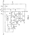
- the invention is exemplified by the diagram of Fig. 2 , which illustrates an inverting DC/DC converter having a positive input voltage V IN , for example five volts, and a negative output voltage V OUT , for example negative eight volts. It should be understood that the invention is applicable to other boost converter circuits that can provide a regulated output voltage, at either polarity, of any particular desired level from any given DC source. Connected in series between input terminal V IN and output terminal V OUT are inductor 110, capacitor 111, and inductor 112. Capacitor 113 is connected between the output terminal and ground.
- Signal responsive switch 114 shown as a transistor, and resistor 115 are connected in series between the circuit point 116, which joins inductor 110 and capacitor 111, and ground.
- Capacitor 111 is connected to inductor 112 at circuit point 117.
- the base of transistor 114 is coupled to the output of latch 120 through switch driver circuit 122.
- a set terminal of the latch is connected to the output of AND gate 124.
- the reset output of the latch is connected to an input of AND gate 124 through delay circuit 126.
- a second input of the AND gate is connected to the output of comparator 128.
- Resistor 130 is connected between the V OUT terminal and a first input of comparator 128.
- the first comparator input also is connected in series with the V IN terminal through reference voltage 132 and resistor 133.
- the voltage applied to the first comparator input thus represents a feedback signal related to the output voltage.
- the second input terminal of comparator 128 is connected to ground.
- a third input of AND gate 24 is connected to the output of comparator 134.
- a first input of comparator 134 is connected to reference voltage 135.
- the second input to comparator 134 is connected to diode 118 at its junction with resistor 119.
- the reset terminal of the latch 120 is connected to the output of comparator 136.
- a first input of comparator 136 is connected to the junction between switch 114 and resistor 115.
- a second input of comparator 136 is connected to reference voltage circuit 137.
- switch 114 turns on and draws current through inductors 110 and 112.
- the current in the inductors ramps up until the voltage across resistor 115 exceeds reference voltage 137, causing comparator 136 to reset the latch and turn off the switch.
- comparator 136 When the switch turns off, inductor current that was flowing through the switch flows instead through diode 118 and resistor 119 to ground. The diode is forward biased and the inductor current ramps down.
- the switch cannot turn on again until a time period set by delay circuit 126 has elapsed.
- the output of feedback comparator 128 is low, indicating that the output voltage is regulated to the desired level, the switch will not turn on. Comparator 128 produces a high output when the output voltage rises above the desired level.
- switch 114 will turn on if the other inputs to AND gate 124 are high.
- the level of the third input to the AND gate 124, the output of comparator 134, is dependent on monitoring the current through diode 118. Current flows through the diode only when the switch 114 is off. Switch turn-on is inhibited by comparator 134 until the diode current ramps below the value set by voltage reference 135 as measured by sensing resistor 119.
- reference voltage values for the circuit described above to provide a regulated output voltage of negative eight volts from a positive DC input of five volts may be 1.250v for reference voltage 132 and 24mv for reference voltages 135 and 137, with appropriate scaling of the other circuit elements.
- the fixed minimum off-time, governed by the delay circuit 126, can be set to a smaller value as compared to conventional arrangements, resulting in smaller external component sizes and higher power densities.
- sensing of the diode current may be achieved using an on-chip resistor element and an integrated schottky diode or, alternatively, using external elements.
- sensing of the diode current may be achieved using an on-chip resistor element and an integrated schottky diode or, alternatively, using external elements.
- the concepts expressed herein with respect to the illustrated inverting regulator circuit are equally applicable to other well known regulators configurations.
Landscapes
- Engineering & Computer Science (AREA)
- Power Engineering (AREA)
- Architecture (AREA)
- Civil Engineering (AREA)
- Structural Engineering (AREA)
- Dc-Dc Converters (AREA)
Description
- The present invention relates to direct current voltage regulators, more particularly to controlled limitation of current in DC/DC converters.
- A conventional step-up DC/DC converter is illustrated in
Fig. 1 .Inductor 10 anddiode 12 are connected in series between input (VIN) and output (VOUT) terminals. The input terminal is typically connected to a DC source, the controlled output connected to a load. Capacitor 14 is connected between the output terminal and ground. Signalresponsive switch 16 andresistor 18 are connected in series between the inductor/diode junction and ground. The switch is represented by a transistor having a base connected to the output oflatch 20 throughswitch driver circuit 22. A set terminal of the latch is connected to the output ofAND gate 24.Delay circuit 26 has an input connected to the reset output of the latch and an output connected to a first input of the AND gate. A second input of the AND gate is connected to the output ofcomparator 28. A first input of the comparator receives a feedback signal related to an output parameter. The output parameter may be the voltage at the output, the feedback signal derived through afeedback circuit 30, the feedback appropriately scaled for comparison with areference voltage 32 applied to a second input of the comparator. The reset terminal of thelatch 20 is connected to the output of asecond comparator 34. A first input ofcomparator 34 is connected to the junction betweenswitch 16 andresistor 18. A second input ofcomparator 34 is connected toreference voltage circuit 36. - In operation, when
switch 16 is in the on, or closed, state, current flows from source VIN throughinductor 10 andresistor 18 to ground.Resistor 18 is a sensing element that provides an indication of the current level through the switch when the switch is closed. When the current through the switch increases to the threshold level ofreference voltage 36,comparator 34 outputs a signal to reset thelatch 20, thereby turning offswitch 16. When the switch is turned off, energy stored in the inductor is transferred to the capacitor 14.Delay circuit 26 ensures that the high latch reset output signal is not applied to the input ofAND gate 24 until a minimum time interval has occurred. Turn-on ofswitch 16 is thus delayed accordingly. Thereafter, the switch will again be turned on when the feedback level exceeds the reference input tocomparator 28. - In the particular conventional circuit illustrated, commonly known as a boost regulator, regulated voltage output VOUT has a voltage level higher in magnitude than the voltage input VIN and of the same polarity. Known converters, for example, are Linear Technology LT3463 and LT3464 converters. With appropriate arrangement of inductor and capacitive elements, a boost regulator output voltage can be provided with a polarity opposite to that of the input voltage.
- In the boost converter configuration, input current through
inductor 10 is continuous, flowing either throughswitch 16 ordiode 12. With a fixed minimum off-time of theswitch 16, the current in the inductor can exceed the maximum current capability of the switch. Such situation can occur, for example, during a short circuit of the output to ground, during the charging of the capacitor 14 immediately after power is applied to the circuit, or any such charging of other circuit capacitors upon initial operation. The switch must turn on for a finite time to sample the inductor current before it can be determined by means ofcomparator 34 that the current exceeds the current limit threshold ofreference 36. During the off-time of the switch, the inductor current does not ramp down as much as it increased during the short on-time because of the small reverse voltage across the inductor. Excessive switch current thus can occur and cause damage or destruction to the regulator as well as the switch. - Prior methods of dealing with the possibility of excessive inductor current have been known in general as frequency foldback provisions. These methods sense a low output feedback condition and accordingly increase an oscillator period in the control circuit of the switch, or increase the delay period, to lengthen the switch off-time by a fixed amount. Frequency foldback methods are disadvantageous in that the increased off-time may not be sufficient to prevent switch current runaway. Because of the uncertainty about external element values, the set off-time may be made too long, thereby unnecessarily (VIN) constraining output current capability during normal operation.
- Document
US 2004/004470 A1 discloses a switching power supply device of a hysteresis current mode control system. In a switching regulator of a hysteresis current mode control system, a sense resistor connected in series to a coil is eliminated, a serially connected resistor and a capacitor are connected in parallel to a coil in place of such a sense resistor. Thereby, a potential of a connection node of this resistor and this capacitor is input of a comparator circuit having the hysteresis characteristic for comparison with the reference voltage. Accordingly, a switch may be controlled for ON and OFF states. - Document
US 2003/222627 A1 discloses a switching power supply which uses carrier control and input voltage sensing. An output voltage is monitored to form a carrier signal. The carrier signal is compared to a signal that is representative of the input current in order to control the switching duty cycle. In addition, a signal representative of the input voltage is summed with the signal that is representative of the input current, or with the carrier signal, in order to control the switching duty cycle under light load conditions and conditions in which the input voltage can vary. - Thus, according to an aspect, it is a problem to provide an improved converter, providing an improved implementation for protection against overcurrent conditions in regulator circuits.
- This problem is solved by the a converter circuit having the features disclosed in claim 1 as well as by a method having the features disclosed in claim 4. Preferred embodiments are defined in the dependent claims.
- The present invention fulfills the above-described needs of the prior art. In a converter coupled to a DC voltage input and connectable to a load, a signal responsive switch is coupled between a first circuit point and a second circuit point, preferably a ground power supply terminal. The load voltage is of a polarity inverse to the polarity of the DC voltage input. Current flow is directed by the switch, when in a closed state, to the second circuit point to bypass the load. A regulator circuit has an output coupled to a control input of the switch. The regulator circuit has a first input for receiving a sensed load parameter signal, a second input for receiving a sensed current level signal at the second circuit point when the switch is in its closed state, and a third input for receiving a sensed current level signal at the second circuit point when the switch is in an open state. The sensed load parameter signal may be related to load voltage and obtained from a load voltage feedback circuit coupled to the first regulator circuit input. The third input of the regulator circuit preferably is coupled to a circuit element operable to conduct unidirectional current, such as a diode. The circuit element is connected in series with the ground input power supply terminal. Current through the diode and ground terminal is measured directly during the off-state of the switch to provide the third input to the regulator circuit. A latch circuit has an output coupled to the control input of the switch, a set input terminal coupled to the first input and the third input, and a reset input terminal coupled to the second input through a delay circuit.
- In operation, the first circuit point is coupled by the switch to the second circuit point in response to the load parameter, for example load voltage, exceeding a predetermined level. The first circuit point is decoupled from the second circuit point in response to a current therebetween exceeding a current threshold level during the coupled state. Recoupling of the first circuit point to the second circuit point is delayed thereafter by at least a fixed timed period. During an excessive current condition at the second circuit point, recoupling is inhibited. The off-time of the switch thus is adjusted as much as needed to achieve a target inductor current before the switch is turned on. An oscillator period or fixed off-time thus can then be set to smaller values than in conventional regulators, thus realizing smaller external component sizes and higher power densities.
- Additional advantages of the present invention will become readily apparent to those skilled in this art from the following detailed description, wherein only the preferred embodiment of the invention is shown and described, simply by way of illustration of the best mode contemplated of carrying out the invention. As will be realized, the invention is capable of other and different embodiments, and its several details are capable of modifications in various obvious respects, all without departing from the invention. Accordingly, the drawings and description are to be regarded as illustrative in nature, and not as restrictive.
- The present invention is illustrated by way of example, and not by way of limitation, in the figures of the accompanying drawing and in which like reference numerals refer to similar elements and in which:
-
Fig. 1 is a diagram of a known step-up DC/DC converter. -
Fig. 2 is a diagram of a converter in accordance with the present invention. - The invention is exemplified by the diagram of
Fig. 2 , which illustrates an inverting DC/DC converter having a positive input voltage VIN, for example five volts, and a negative output voltage VOUT, for example negative eight volts. It should be understood that the invention is applicable to other boost converter circuits that can provide a regulated output voltage, at either polarity, of any particular desired level from any given DC source. Connected in series between input terminal VIN and output terminal VOUT are inductor 110,capacitor 111, andinductor 112.Capacitor 113 is connected between the output terminal and ground. Signalresponsive switch 114, shown as a transistor, andresistor 115 are connected in series between thecircuit point 116, which joinsinductor 110 andcapacitor 111, and ground.Capacitor 111 is connected toinductor 112 atcircuit point 117. Connected in series betweencircuit point 117 and ground areschottky diode 1,18 andresistor 119. The base oftransistor 114 is coupled to the output oflatch 120 through switch driver circuit 122. A set terminal of the latch is connected to the output of ANDgate 124. The reset output of the latch is connected to an input of ANDgate 124 throughdelay circuit 126. A second input of the AND gate is connected to the output ofcomparator 128.Resistor 130 is connected between the VOUT terminal and a first input ofcomparator 128. The first comparator input also is connected in series with the VIN terminal throughreference voltage 132 andresistor 133. The voltage applied to the first comparator input thus represents a feedback signal related to the output voltage. The second input terminal ofcomparator 128 is connected to ground. A third input of ANDgate 24 is connected to the output ofcomparator 134. A first input ofcomparator 134 is connected toreference voltage 135. The second input tocomparator 134 is connected todiode 118 at its junction withresistor 119. The reset terminal of thelatch 120 is connected to the output ofcomparator 136. A first input ofcomparator 136 is connected to the junction betweenswitch 114 andresistor 115. A second input ofcomparator 136 is connected to referencevoltage circuit 137. - During a switch cycle, switch 114 turns on and draws current through
inductors resistor 115 exceedsreference voltage 137, causingcomparator 136 to reset the latch and turn off the switch. When the switch turns off, inductor current that was flowing through the switch flows instead throughdiode 118 andresistor 119 to ground. The diode is forward biased and the inductor current ramps down. The switch cannot turn on again until a time period set bydelay circuit 126 has elapsed. When the output offeedback comparator 128 is low, indicating that the output voltage is regulated to the desired level, the switch will not turn on.Comparator 128 produces a high output when the output voltage rises above the desired level. At that time,switch 114 will turn on if the other inputs to ANDgate 124 are high. The level of the third input to the ANDgate 124, the output ofcomparator 134, is dependent on monitoring the current throughdiode 118. Current flows through the diode only when theswitch 114 is off. Switch turn-on is inhibited bycomparator 134 until the diode current ramps below the value set byvoltage reference 135 as measured by sensingresistor 119. - By way of example, reference voltage values for the circuit described above to provide a regulated output voltage of negative eight volts from a positive DC input of five volts may be 1.250v for
reference voltage 132 and 24mv forreference voltages delay circuit 126, can be set to a smaller value as compared to conventional arrangements, resulting in smaller external component sizes and higher power densities. - In this disclosure there are shown and described only preferred embodiments of the invention and but a few examples of its versatility. It is to be understood that the invention is capable of use in various other combinations and environments and is capable of changes or modifications within the scope of the inventive concept as expressed herein. For example, sensing of the diode current may be achieved using an on-chip resistor element and an integrated schottky diode or, alternatively, using external elements. The concepts expressed herein with respect to the illustrated inverting regulator circuit are equally applicable to other well known regulators configurations.
Claims (4)
- An inverting converter circuit having an input terminal to receive an input DC voltage at a first voltage level and having an output terminal to provide an output DC voltage at a second voltage level to a load, comprising:a first inductor (110) connected to the input terminal;a second inductor (112) connected to the output terminal;a capacitor (111) connected between the first inductor (110) and the second inductor (112) in series;a switch (114) coupled between a first circuit point (116) and a second circuit point, the first circuit point (116) joining the first inductor (110) and the capacitor (111), the second circuit point being preferably ground;a first current flow path when the switch (114) is in an on-state, the first current flow path bypassing the load;a second current flow path when the switch (114) is in an off-state, the second current flow path including a unidirectional current conducting device (118) connected between a third circuit point (117) and the second circuit point, the third circuit point joining the capacitor (111) and the second inductor (112); anda control circuit coupled to the switch (114) and configured to receive signals related respectively to a load parameter, current through the switch (114) when the switch (114) is in the on-state and current through the unidirectional current conducting device (118) when the switch (114) is in the off-state, and in response, controlling the state of the switch (114),wherein the control circuit initiates the off-state switch (114) condition when the switch current attains a prescribed level, and the control circuit comprises a delay circuit (126) for maintaining the off-state of the switch (114) for a fixed time period,wherein the control circuit initiates transition of the switch (114) from off-state condition to the on-state condition after the fixed time period when the load parameter exceeds a threshold level, andwherein said transition is inhibited when the current through the unidirectional current conducting device is at an excessive level.
- A converter circuit as recited in claim 1, further comprising a load voltage feedback circuit coupled between the load and the control circuit, and wherein the load parameter is load voltage.
- A converter circuit as recited in claim 1, wherein the output DC voltage is inverted in polarity from the polarity of the input DC voltage.
- A method of controlling an inverting converter circuit having an input terminal to receive an input DC voltage at a first voltage level, an output terminal to provide an output DC voltage at a second voltage level to a load, a first inductor (110) connected to the input terminal, a second inductor (112) connected to the output terminal, a capacitor (111) connected between the first and second inductors in series, and a switch (114) coupled between a first circuit point (116) and a second circuit point, the first circuit point (116) joining the first inductor (110) and the capacitor (111), the second circuit point being preferably ground; the method comprising the steps of:- providing a first current flow path when the switch is an on-state, the first current flow path bypassing the load;- providing a second current flow path when the switch is an off-state, the second flow path including a unidirectional current conducting device (118) connected between a third circuit point (117) and the second circuit point, the third circuit point joining the capacitor (111) and the second inductor (112); and- controlling the switch in response to signals related respectively to a load parameter, current through the switch when the switch is in the on-state and current through the unidirectional current conducting device (118) when the switch is in the off-state,- initiating the off-state switch condition when the switch current attains a prescribed level,- maintaining the off-state of the switch for a fixed time period,- initiating transition of the switch from off-state condition to the on-state condition after the fixed time period when the load parameter exceeds a threshold level, and- inhibiting said transition when the current through the unidirectional current conducting device is at an excessive level.
Applications Claiming Priority (1)
| Application Number | Priority Date | Filing Date | Title |
|---|---|---|---|
| US11/030,993 US7710700B2 (en) | 2005-01-10 | 2005-01-10 | DC/DC converter with current limit protection |
Publications (3)
| Publication Number | Publication Date |
|---|---|
| EP1679780A2 EP1679780A2 (en) | 2006-07-12 |
| EP1679780A3 EP1679780A3 (en) | 2009-11-25 |
| EP1679780B1 true EP1679780B1 (en) | 2017-08-30 |
Family
ID=36128497
Family Applications (1)
| Application Number | Title | Priority Date | Filing Date |
|---|---|---|---|
| EP06250081.4A Expired - Lifetime EP1679780B1 (en) | 2005-01-10 | 2006-01-09 | DC/DC converter with current limit protection |
Country Status (4)
| Country | Link |
|---|---|
| US (1) | US7710700B2 (en) |
| EP (1) | EP1679780B1 (en) |
| JP (1) | JP4864463B2 (en) |
| KR (1) | KR101185410B1 (en) |
Families Citing this family (17)
| Publication number | Priority date | Publication date | Assignee | Title |
|---|---|---|---|---|
| US7710700B2 (en) * | 2005-01-10 | 2010-05-04 | Linear Technology Corporation | DC/DC converter with current limit protection |
| JP4777730B2 (en) * | 2005-09-20 | 2011-09-21 | セイコーインスツル株式会社 | DC-DC converter |
| CN101350614B (en) * | 2007-07-17 | 2012-05-16 | 鸿富锦精密工业(深圳)有限公司 | Control circuit for electric timing switch |
| US7843248B1 (en) * | 2007-11-01 | 2010-11-30 | Intersil Americas Inc. | Analog switch with overcurrent detection |
| JP5038922B2 (en) * | 2008-01-23 | 2012-10-03 | トヨタ自動車株式会社 | Power supply device and vehicle including the same |
| KR101507405B1 (en) * | 2008-12-30 | 2015-04-06 | 주식회사 동부하이텍 | Current Mode DC Direct Current Converter |
| EP2325986A1 (en) * | 2009-11-23 | 2011-05-25 | Dialog Semiconductor GmbH | Automatic current limit adjustment for linear and switching regulators |
| JP5067430B2 (en) * | 2010-02-02 | 2012-11-07 | 日本テキサス・インスツルメンツ株式会社 | Converter circuit |
| CN102934340B (en) * | 2010-03-31 | 2016-06-29 | 黑拉许克联合股份有限公司 | There is direct current transducer and the load current collection of Cuk circuit |
| DE102010061042A1 (en) * | 2010-12-06 | 2012-06-06 | Hella Kgaa Hueck & Co. | DC-DC converter with circuit for simulating a current through a storage choke |
| US8427130B2 (en) | 2010-12-16 | 2013-04-23 | Integrated Device Technology, Inc. | Methods and apparatuses for combined frequency compensation and soft start processes |
| US8513935B2 (en) | 2010-12-16 | 2013-08-20 | Integrated Device Technology, Inc. | Combinations of current feedback for frequency compensation, overload detection, and super overload detection in switching power converters |
| US20140192449A1 (en) * | 2011-07-14 | 2014-07-10 | Fuji Electric Co., Ltd. | Short-circuit protection circuit |
| KR101285295B1 (en) * | 2012-04-16 | 2013-07-11 | 순천향대학교 산학협력단 | Boost dc-dc converter |
| TWI573006B (en) * | 2015-06-18 | 2017-03-01 | 英特爾股份有限公司 | Power supplier, power supply system, and voltage adjustment method |
| CN113517809B (en) * | 2021-04-25 | 2022-07-12 | 中国电子科技集团公司第五十八研究所 | Fast booster circuit and control method thereof |
| US12341427B2 (en) | 2022-03-15 | 2025-06-24 | Texas Instruments Incorporated | Skip clamp circuit for DC-DC power converters |
Family Cites Families (12)
| Publication number | Priority date | Publication date | Assignee | Title |
|---|---|---|---|---|
| US5028861A (en) * | 1989-05-24 | 1991-07-02 | Motorola, Inc. | Strobed DC-DC converter with current regulation |
| JP2547652B2 (en) * | 1990-05-15 | 1996-10-23 | 三洋電機株式会社 | Power converter |
| JP3258137B2 (en) * | 1993-06-25 | 2002-02-18 | 株式会社日立製作所 | Motor drive |
| IT1268474B1 (en) * | 1993-10-22 | 1997-03-04 | St Microelectronics Srl | DC-DC STATIC CONVERTER WORKING IN DISCONTINUOUS MODE |
| US5708578A (en) * | 1995-07-19 | 1998-01-13 | Stoddard; Robert J. | PWM inductive load bridge driver for dynamically mixing four and two quadrant chopping during PWM period off time |
| US5912552A (en) * | 1997-02-12 | 1999-06-15 | Kabushiki Kaisha Toyoda Jidoshokki Seisakusho | DC to DC converter with high efficiency for light loads |
| DE60210217T2 (en) | 2001-01-31 | 2006-11-16 | Matsushita Electric Industrial Co., Ltd., Kadoma | SMPS device |
| US6657417B1 (en) | 2002-05-31 | 2003-12-02 | Champion Microelectronic Corp. | Power factor correction with carrier control and input voltage sensing |
| JP4364554B2 (en) * | 2002-06-07 | 2009-11-18 | 株式会社ルネサステクノロジ | Switching power supply device and switching power supply system |
| JP2004364488A (en) * | 2003-05-12 | 2004-12-24 | Taiyo Yuden Co Ltd | Switching power supply circuit and overcurrent protection method therefor |
| JP3748262B2 (en) | 2003-06-24 | 2006-02-22 | ローム株式会社 | Switching type DC-DC converter |
| US7710700B2 (en) * | 2005-01-10 | 2010-05-04 | Linear Technology Corporation | DC/DC converter with current limit protection |
-
2005
- 2005-01-10 US US11/030,993 patent/US7710700B2/en active Active
-
2006
- 2006-01-05 JP JP2006000779A patent/JP4864463B2/en not_active Expired - Lifetime
- 2006-01-09 EP EP06250081.4A patent/EP1679780B1/en not_active Expired - Lifetime
- 2006-01-10 KR KR1020060002854A patent/KR101185410B1/en not_active Expired - Lifetime
Non-Patent Citations (1)
| Title |
|---|
| SANTI E ET AL: "Low-distortion control of unity-power-factor converters in discontinuous conduction mode", POWER ELECTRONICS SPECIALISTS CONFERENCE, 1999. PESC 99. 30TH ANNUAL I EEE CHARLESTON, SC, USA 27 JUNE-1 JULY 1999, PISCATAWAY, NJ, USA,IEEE, US, vol. 1, 27 June 1999 (1999-06-27), pages 301 - 306, XP010346857, ISBN: 978-0-7803-5421-0, DOI: 10.1109/PESC.1999.789019 * |
Also Published As
| Publication number | Publication date |
|---|---|
| KR20060081668A (en) | 2006-07-13 |
| US20060152874A1 (en) | 2006-07-13 |
| EP1679780A3 (en) | 2009-11-25 |
| JP2006197794A (en) | 2006-07-27 |
| US7710700B2 (en) | 2010-05-04 |
| JP4864463B2 (en) | 2012-02-01 |
| KR101185410B1 (en) | 2012-09-25 |
| EP1679780A2 (en) | 2006-07-12 |
Similar Documents
| Publication | Publication Date | Title |
|---|---|---|
| US7710700B2 (en) | DC/DC converter with current limit protection | |
| US10581328B2 (en) | Synchronous rectifier for buck converter without the need for a comparator | |
| JP4908386B2 (en) | Switching power supply device and driving method thereof | |
| EP1689070B1 (en) | Current-mode control for switched step up-step down regulators | |
| US7068023B2 (en) | Switching power supply circuit and overcurrent protection method for the switching power supply circuit | |
| JP5125066B2 (en) | Control circuit for synchronous rectification type DC-DC converter, synchronous rectification type DC-DC converter and control method therefor | |
| US9698691B2 (en) | Circuit and method for maximum duty cycle limitation in switching converters | |
| EP1689068B1 (en) | Light load current-mode control for switched step up-step down regulators | |
| US7161333B2 (en) | System and method for determining load current in switching regulators operable in pulse skipping mode | |
| US7782030B2 (en) | Step-down converter | |
| US7915881B2 (en) | Buck DC-to-DC converter and method | |
| US20180262118A1 (en) | Resonant converter with improved light load efficiency and the method thereof | |
| US7816896B2 (en) | Circuits and methods for controlling a converter | |
| JP2009136105A5 (en) | ||
| CN107408884B (en) | Power conversion device and control method for power conversion device | |
| US11594966B2 (en) | Load driving device with failure detection | |
| US9559593B2 (en) | Synchronous rectification converter and control method of synchronous rectification converter | |
| US20210194367A1 (en) | Dc-dc converter circuit | |
| JP2007053892A (en) | DC-DC converter | |
| CN110943506B (en) | Auxiliary power socket with load inductance measurement system | |
| US10931198B2 (en) | Buck-boost power converter controller | |
| JP2017131033A (en) | Switching power supply device | |
| JP3289680B2 (en) | Power supply inrush current prevention circuit | |
| JP2009038894A (en) | Power control circuit | |
| US20250357846A1 (en) | Dc/dc converter operable efficiently while preventing reverse current |
Legal Events
| Date | Code | Title | Description |
|---|---|---|---|
| PUAI | Public reference made under article 153(3) epc to a published international application that has entered the european phase |
Free format text: ORIGINAL CODE: 0009012 |
|
| AK | Designated contracting states |
Kind code of ref document: A2 Designated state(s): AT BE BG CH CY CZ DE DK EE ES FI FR GB GR HU IE IS IT LI LT LU LV MC NL PL PT RO SE SI SK TR |
|
| AX | Request for extension of the european patent |
Extension state: AL BA HR MK YU |
|
| PUAL | Search report despatched |
Free format text: ORIGINAL CODE: 0009013 |
|
| AK | Designated contracting states |
Kind code of ref document: A3 Designated state(s): AT BE BG CH CY CZ DE DK EE ES FI FR GB GR HU IE IS IT LI LT LU LV MC NL PL PT RO SE SI SK TR |
|
| AX | Request for extension of the european patent |
Extension state: AL BA HR MK YU |
|
| 17P | Request for examination filed |
Effective date: 20100304 |
|
| 17Q | First examination report despatched |
Effective date: 20100326 |
|
| AKX | Designation fees paid |
Designated state(s): AT BE BG CH CY CZ DE DK EE ES FI FR GB GR HU IE IS IT LI LT LU LV MC NL PL PT RO SE SI SK TR |
|
| RAP1 | Party data changed (applicant data changed or rights of an application transferred) |
Owner name: LINEAR TECHNOLOGY CORPORATION |
|
| REG | Reference to a national code |
Ref country code: DE Ref legal event code: R079 Ref document number: 602006053450 Country of ref document: DE Free format text: PREVIOUS MAIN CLASS: H02M0003070000 Ipc: H02M0001320000 |
|
| GRAP | Despatch of communication of intention to grant a patent |
Free format text: ORIGINAL CODE: EPIDOSNIGR1 |
|
| RIC1 | Information provided on ipc code assigned before grant |
Ipc: H02M 3/156 20060101ALI20170306BHEP Ipc: H02M 1/32 20070101AFI20170306BHEP |
|
| INTG | Intention to grant announced |
Effective date: 20170323 |
|
| GRAS | Grant fee paid |
Free format text: ORIGINAL CODE: EPIDOSNIGR3 |
|
| GRAA | (expected) grant |
Free format text: ORIGINAL CODE: 0009210 |
|
| AK | Designated contracting states |
Kind code of ref document: B1 Designated state(s): AT BE BG CH CY CZ DE DK EE ES FI FR GB GR HU IE IS IT LI LT LU LV MC NL PL PT RO SE SI SK TR |
|
| REG | Reference to a national code |
Ref country code: DE Ref legal event code: R081 Ref document number: 602006053450 Country of ref document: DE Owner name: ANALOG DEVICES INTERNATIONAL UNLIMITED COMPANY, IE Free format text: FORMER OWNER: LINEAR TECHNOLOGY CORP., MILPITAS, CALIF., US Ref country code: GB Ref legal event code: FG4D |
|
| REG | Reference to a national code |
Ref country code: CH Ref legal event code: EP |
|
| REG | Reference to a national code |
Ref country code: AT Ref legal event code: REF Ref document number: 924521 Country of ref document: AT Kind code of ref document: T Effective date: 20170915 |
|
| REG | Reference to a national code |
Ref country code: IE Ref legal event code: FG4D |
|
| REG | Reference to a national code |
Ref country code: DE Ref legal event code: R096 Ref document number: 602006053450 Country of ref document: DE |
|
| REG | Reference to a national code |
Ref country code: NL Ref legal event code: FP |
|
| REG | Reference to a national code |
Ref country code: FR Ref legal event code: PLFP Year of fee payment: 13 |
|
| REG | Reference to a national code |
Ref country code: LT Ref legal event code: MG4D |
|
| REG | Reference to a national code |
Ref country code: AT Ref legal event code: MK05 Ref document number: 924521 Country of ref document: AT Kind code of ref document: T Effective date: 20170830 |
|
| PG25 | Lapsed in a contracting state [announced via postgrant information from national office to epo] |
Ref country code: LT Free format text: LAPSE BECAUSE OF FAILURE TO SUBMIT A TRANSLATION OF THE DESCRIPTION OR TO PAY THE FEE WITHIN THE PRESCRIBED TIME-LIMIT Effective date: 20170830 Ref country code: AT Free format text: LAPSE BECAUSE OF FAILURE TO SUBMIT A TRANSLATION OF THE DESCRIPTION OR TO PAY THE FEE WITHIN THE PRESCRIBED TIME-LIMIT Effective date: 20170830 Ref country code: FI Free format text: LAPSE BECAUSE OF FAILURE TO SUBMIT A TRANSLATION OF THE DESCRIPTION OR TO PAY THE FEE WITHIN THE PRESCRIBED TIME-LIMIT Effective date: 20170830 Ref country code: SE Free format text: LAPSE BECAUSE OF FAILURE TO SUBMIT A TRANSLATION OF THE DESCRIPTION OR TO PAY THE FEE WITHIN THE PRESCRIBED TIME-LIMIT Effective date: 20170830 |
|
| PG25 | Lapsed in a contracting state [announced via postgrant information from national office to epo] |
Ref country code: LV Free format text: LAPSE BECAUSE OF FAILURE TO SUBMIT A TRANSLATION OF THE DESCRIPTION OR TO PAY THE FEE WITHIN THE PRESCRIBED TIME-LIMIT Effective date: 20170830 Ref country code: IS Free format text: LAPSE BECAUSE OF FAILURE TO SUBMIT A TRANSLATION OF THE DESCRIPTION OR TO PAY THE FEE WITHIN THE PRESCRIBED TIME-LIMIT Effective date: 20171230 Ref country code: ES Free format text: LAPSE BECAUSE OF FAILURE TO SUBMIT A TRANSLATION OF THE DESCRIPTION OR TO PAY THE FEE WITHIN THE PRESCRIBED TIME-LIMIT Effective date: 20170830 Ref country code: BG Free format text: LAPSE BECAUSE OF FAILURE TO SUBMIT A TRANSLATION OF THE DESCRIPTION OR TO PAY THE FEE WITHIN THE PRESCRIBED TIME-LIMIT Effective date: 20171130 Ref country code: GR Free format text: LAPSE BECAUSE OF FAILURE TO SUBMIT A TRANSLATION OF THE DESCRIPTION OR TO PAY THE FEE WITHIN THE PRESCRIBED TIME-LIMIT Effective date: 20171201 |
|
| PG25 | Lapsed in a contracting state [announced via postgrant information from national office to epo] |
Ref country code: PL Free format text: LAPSE BECAUSE OF FAILURE TO SUBMIT A TRANSLATION OF THE DESCRIPTION OR TO PAY THE FEE WITHIN THE PRESCRIBED TIME-LIMIT Effective date: 20170830 Ref country code: DK Free format text: LAPSE BECAUSE OF FAILURE TO SUBMIT A TRANSLATION OF THE DESCRIPTION OR TO PAY THE FEE WITHIN THE PRESCRIBED TIME-LIMIT Effective date: 20170830 Ref country code: CZ Free format text: LAPSE BECAUSE OF FAILURE TO SUBMIT A TRANSLATION OF THE DESCRIPTION OR TO PAY THE FEE WITHIN THE PRESCRIBED TIME-LIMIT Effective date: 20170830 Ref country code: RO Free format text: LAPSE BECAUSE OF FAILURE TO SUBMIT A TRANSLATION OF THE DESCRIPTION OR TO PAY THE FEE WITHIN THE PRESCRIBED TIME-LIMIT Effective date: 20170830 |
|
| PG25 | Lapsed in a contracting state [announced via postgrant information from national office to epo] |
Ref country code: EE Free format text: LAPSE BECAUSE OF FAILURE TO SUBMIT A TRANSLATION OF THE DESCRIPTION OR TO PAY THE FEE WITHIN THE PRESCRIBED TIME-LIMIT Effective date: 20170830 Ref country code: SK Free format text: LAPSE BECAUSE OF FAILURE TO SUBMIT A TRANSLATION OF THE DESCRIPTION OR TO PAY THE FEE WITHIN THE PRESCRIBED TIME-LIMIT Effective date: 20170830 |
|
| REG | Reference to a national code |
Ref country code: DE Ref legal event code: R097 Ref document number: 602006053450 Country of ref document: DE |
|
| PLBE | No opposition filed within time limit |
Free format text: ORIGINAL CODE: 0009261 |
|
| STAA | Information on the status of an ep patent application or granted ep patent |
Free format text: STATUS: NO OPPOSITION FILED WITHIN TIME LIMIT |
|
| 26N | No opposition filed |
Effective date: 20180531 |
|
| PG25 | Lapsed in a contracting state [announced via postgrant information from national office to epo] |
Ref country code: SI Free format text: LAPSE BECAUSE OF FAILURE TO SUBMIT A TRANSLATION OF THE DESCRIPTION OR TO PAY THE FEE WITHIN THE PRESCRIBED TIME-LIMIT Effective date: 20170830 |
|
| REG | Reference to a national code |
Ref country code: CH Ref legal event code: PL |
|
| PG25 | Lapsed in a contracting state [announced via postgrant information from national office to epo] |
Ref country code: LU Free format text: LAPSE BECAUSE OF NON-PAYMENT OF DUE FEES Effective date: 20180109 |
|
| REG | Reference to a national code |
Ref country code: IE Ref legal event code: MM4A |
|
| REG | Reference to a national code |
Ref country code: BE Ref legal event code: MM Effective date: 20180131 |
|
| PG25 | Lapsed in a contracting state [announced via postgrant information from national office to epo] |
Ref country code: CH Free format text: LAPSE BECAUSE OF NON-PAYMENT OF DUE FEES Effective date: 20180131 Ref country code: LI Free format text: LAPSE BECAUSE OF NON-PAYMENT OF DUE FEES Effective date: 20180131 Ref country code: BE Free format text: LAPSE BECAUSE OF NON-PAYMENT OF DUE FEES Effective date: 20180131 |
|
| PG25 | Lapsed in a contracting state [announced via postgrant information from national office to epo] |
Ref country code: IE Free format text: LAPSE BECAUSE OF NON-PAYMENT OF DUE FEES Effective date: 20180109 |
|
| PG25 | Lapsed in a contracting state [announced via postgrant information from national office to epo] |
Ref country code: MC Free format text: LAPSE BECAUSE OF FAILURE TO SUBMIT A TRANSLATION OF THE DESCRIPTION OR TO PAY THE FEE WITHIN THE PRESCRIBED TIME-LIMIT Effective date: 20170830 |
|
| PG25 | Lapsed in a contracting state [announced via postgrant information from national office to epo] |
Ref country code: TR Free format text: LAPSE BECAUSE OF FAILURE TO SUBMIT A TRANSLATION OF THE DESCRIPTION OR TO PAY THE FEE WITHIN THE PRESCRIBED TIME-LIMIT Effective date: 20170830 |
|
| PG25 | Lapsed in a contracting state [announced via postgrant information from national office to epo] |
Ref country code: HU Free format text: LAPSE BECAUSE OF FAILURE TO SUBMIT A TRANSLATION OF THE DESCRIPTION OR TO PAY THE FEE WITHIN THE PRESCRIBED TIME-LIMIT; INVALID AB INITIO Effective date: 20060109 Ref country code: PT Free format text: LAPSE BECAUSE OF FAILURE TO SUBMIT A TRANSLATION OF THE DESCRIPTION OR TO PAY THE FEE WITHIN THE PRESCRIBED TIME-LIMIT Effective date: 20170830 |
|
| PG25 | Lapsed in a contracting state [announced via postgrant information from national office to epo] |
Ref country code: CY Free format text: LAPSE BECAUSE OF FAILURE TO SUBMIT A TRANSLATION OF THE DESCRIPTION OR TO PAY THE FEE WITHIN THE PRESCRIBED TIME-LIMIT Effective date: 20170830 |
|
| REG | Reference to a national code |
Ref country code: DE Ref legal event code: R082 Ref document number: 602006053450 Country of ref document: DE Representative=s name: MUELLER-BORE & PARTNER PATENTANWAELTE PARTG MB, DE Ref country code: DE Ref legal event code: R081 Ref document number: 602006053450 Country of ref document: DE Owner name: ANALOG DEVICES INTERNATIONAL UNLIMITED COMPANY, IE Free format text: FORMER OWNER: LINEAR TECHNOLOGY CORPORATION, MILPITAS, CALIF., US Ref country code: DE Ref legal event code: R082 Ref document number: 602006053450 Country of ref document: DE Representative=s name: WITHERS & ROGERS LLP, DE |
|
| REG | Reference to a national code |
Ref country code: DE Ref legal event code: R082 Ref document number: 602006053450 Country of ref document: DE Representative=s name: WITHERS & ROGERS LLP, DE |
|
| REG | Reference to a national code |
Ref country code: GB Ref legal event code: 732E Free format text: REGISTERED BETWEEN 20211118 AND 20211124 |
|
| REG | Reference to a national code |
Ref country code: NL Ref legal event code: PD Owner name: ANALOG DEVICES INTERNATIONAL UNLIMITED COMPANY; IE Free format text: DETAILS ASSIGNMENT: CHANGE OF OWNER(S), ASSIGNMENT; FORMER OWNER NAME: LINEAR TECHNOLOGY LLC Effective date: 20211216 |
|
| PGFP | Annual fee paid to national office [announced via postgrant information from national office to epo] |
Ref country code: GB Payment date: 20211216 Year of fee payment: 17 Ref country code: FR Payment date: 20211215 Year of fee payment: 17 |
|
| PGFP | Annual fee paid to national office [announced via postgrant information from national office to epo] |
Ref country code: NL Payment date: 20211216 Year of fee payment: 17 |
|
| PGFP | Annual fee paid to national office [announced via postgrant information from national office to epo] |
Ref country code: DE Payment date: 20211215 Year of fee payment: 17 |
|
| PGFP | Annual fee paid to national office [announced via postgrant information from national office to epo] |
Ref country code: IT Payment date: 20220103 Year of fee payment: 17 |
|
| REG | Reference to a national code |
Ref country code: DE Ref legal event code: R119 Ref document number: 602006053450 Country of ref document: DE |
|
| REG | Reference to a national code |
Ref country code: NL Ref legal event code: MM Effective date: 20230201 |
|
| GBPC | Gb: european patent ceased through non-payment of renewal fee |
Effective date: 20230109 |
|
| PG25 | Lapsed in a contracting state [announced via postgrant information from national office to epo] |
Ref country code: NL Free format text: LAPSE BECAUSE OF NON-PAYMENT OF DUE FEES Effective date: 20230201 Ref country code: GB Free format text: LAPSE BECAUSE OF NON-PAYMENT OF DUE FEES Effective date: 20230109 Ref country code: DE Free format text: LAPSE BECAUSE OF NON-PAYMENT OF DUE FEES Effective date: 20230801 |
|
| PG25 | Lapsed in a contracting state [announced via postgrant information from national office to epo] |
Ref country code: FR Free format text: LAPSE BECAUSE OF NON-PAYMENT OF DUE FEES Effective date: 20230131 |
|
| PG25 | Lapsed in a contracting state [announced via postgrant information from national office to epo] |
Ref country code: IT Free format text: LAPSE BECAUSE OF NON-PAYMENT OF DUE FEES Effective date: 20230109 |