EP1677355A2 - Process for manufacturing an image sensor using deuterium - Google Patents
Process for manufacturing an image sensor using deuterium Download PDFInfo
- Publication number
- EP1677355A2 EP1677355A2 EP20050257877 EP05257877A EP1677355A2 EP 1677355 A2 EP1677355 A2 EP 1677355A2 EP 20050257877 EP20050257877 EP 20050257877 EP 05257877 A EP05257877 A EP 05257877A EP 1677355 A2 EP1677355 A2 EP 1677355A2
- Authority
- EP
- European Patent Office
- Prior art keywords
- deuterium
- image sensor
- forming
- pixel array
- semiconductor devices
- Prior art date
- Legal status (The legal status is an assumption and is not a legal conclusion. Google has not performed a legal analysis and makes no representation as to the accuracy of the status listed.)
- Ceased
Links
Images

Classifications
-
- H—ELECTRICITY
- H10—SEMICONDUCTOR DEVICES; ELECTRIC SOLID-STATE DEVICES NOT OTHERWISE PROVIDED FOR
- H10F—INORGANIC SEMICONDUCTOR DEVICES SENSITIVE TO INFRARED RADIATION, LIGHT, ELECTROMAGNETIC RADIATION OF SHORTER WAVELENGTH OR CORPUSCULAR RADIATION
- H10F39/00—Integrated devices, or assemblies of multiple devices, comprising at least one element covered by group H10F30/00, e.g. radiation detectors comprising photodiode arrays
- H10F39/011—Manufacture or treatment of image sensors covered by group H10F39/12
- H10F39/014—Manufacture or treatment of image sensors covered by group H10F39/12 of CMOS image sensors
-
- H—ELECTRICITY
- H10—SEMICONDUCTOR DEVICES; ELECTRIC SOLID-STATE DEVICES NOT OTHERWISE PROVIDED FOR
- H10F—INORGANIC SEMICONDUCTOR DEVICES SENSITIVE TO INFRARED RADIATION, LIGHT, ELECTROMAGNETIC RADIATION OF SHORTER WAVELENGTH OR CORPUSCULAR RADIATION
- H10F39/00—Integrated devices, or assemblies of multiple devices, comprising at least one element covered by group H10F30/00, e.g. radiation detectors comprising photodiode arrays
- H10F39/10—Integrated devices
- H10F39/12—Image sensors
- H10F39/18—Complementary metal-oxide-semiconductor [CMOS] image sensors; Photodiode array image sensors
-
- H—ELECTRICITY
- H10—SEMICONDUCTOR DEVICES; ELECTRIC SOLID-STATE DEVICES NOT OTHERWISE PROVIDED FOR
- H10F—INORGANIC SEMICONDUCTOR DEVICES SENSITIVE TO INFRARED RADIATION, LIGHT, ELECTROMAGNETIC RADIATION OF SHORTER WAVELENGTH OR CORPUSCULAR RADIATION
- H10F71/00—Manufacture or treatment of devices covered by this subclass
Definitions
- the present invention relates to image sensors, and more particularly, to an image sensor that uses an improved deuterium (D2) alloy process.
- D2 deuterium
- Image sensors have become ubiquitous. They are widely used in digital still cameras, cellular phones, security cameras, medical, automobile, and other applications.
- the technology used to manufacture image sensors, and in particular CMOS image sensors, has continued to advance at great pace. For example, the demands of higher resolution and lower power consumption have encouraged the further miniaturization and integration of the image sensor.
- CHC channel hot carrier
- the semiconductor wafers are typically exposed to a combination of nitrogen (N 2 ) and hydrogen (H 2 ) gases in a furnace at a temperature of around 400-450 C.
- N 2 nitrogen
- H 2 hydrogen
- This process is performed as part of a passivation process or after etching of the bond pads of the image sensor.
- the metal layers of the image sensor have already been defined and patterned. The metal layers are typically detrimentally affected by temperatures greater than 400-450 °C.
- the present invention provides a method of alloying an image sensor according to Claim 1..
- Figure 1 shows a cross-sectional view of a prior art image sensor.
- a portion 101 of an image sensor is shown.
- the portion 101 of the image sensor includes a pixel array section 103, an n-channel periphery area 105, and a p-channel periphery area 107.
- the n-channel periphery area 105 and p-channel periphery area 107 contains those elements of the image sensor outside of the pixel array 103.
- the periphery areas 105 and 107 are used to form various control, logic, signal processing, readout, and other types of integrated circuitry.
- the transistors shown in areas 105 and 107 of course are merely exemplar and these areas would normally contain many transistors (PMOS and NMOS).
- the pixel array section 103 only shows one example of a pixel, and is meant to be representative of a pixel array.
- the pixel array would include photosensitive elements, such as those chosen from the group of a photodiode, partially pinned photodiode, pinned photodiode, photogate, or photocapacitor.
- an insulating oxide layer 201 is blanket deposited over the surface of the image sensor.
- the insulator may be spin on glass (SOG), borophosphosilicate glass (BPSG), phosphosilicate glass (PSG), or undoped silicate glass (USG).
- the image sensor is alloyed using deuterium gas, which is a naturally occurring isotope of hydrogen.
- deuterium gas which is a naturally occurring isotope of hydrogen.
- this alloying process takes places prior to the deposition and etching of any metal layers and thus, does not deteriorate the metal layers.
- high energy (hot) electrons can impact the surface and dislodge hydrogen atoms (from conventional prior art alloying) and re-create surface state traps.
- the deuterium isotope of hydrogen is twice as heavy as hydrogen, and it is believed that the deuterium is much more difficult for the hot electrons to dislodge. For this or whatever physical reason, the hot electron lifetime under hot electron stress conditions (low temperature, high voltage stress) can be improved using a deuterium alloy.
- the alloying process using the deuterium is performed after deposition of the blanket insulator layer over the semiconductor substrate and transistor gates.
- the alloying process typically takes place in a furnace tube.
- the alloying process takes place under one atmospheric pressure with a 5% deuterium mix in nitrogen to a 100% deuterium mix in the ambient.
- the temperature is in the range of 300 - 900 °C, and preferably between 500 - 800 °C.
- the deuterium alloying process is performed after planerization of the insulator oxide layer 201.
- the insulator layer 201 has been planerized to remove irregularities in the topology of the oxide.
- the planarization step is a common step used to aid in the manufacturing process and can be performed using a chemical mechanical polishing (CMP) or an etching back process.
- CMP chemical mechanical polishing
- the deuterium alloying process is performed after openings have been made in the insulator layer 201.
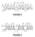
- the openings 401 are typically made in order to allow contact plugs to be formed in the insulator layer that contact various active regions in the substrate or to contact the polysilicon gates of the transistors. Thus, in Figure 4, the openings 401 will eventually be filled with contact plugs.
- the deuterium alloying process is performed after the masking and etching of the insulator oxide layer 201.
- the deuterium alloying process may be performed.
- the deuterium alloying is performed prior to deposition of the metal layer for formation of the interconnect. This is an advantage over the prior art which results in deterioration of the metal interconnect layer.
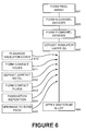
- Figure 6 illustrates in flow diagram a method of the present invention.
- a pixel array is formed in a semiconductor substrate.
- semiconductor devices such as transistors, memory, capacitors, etc.... are formed in the n-channel periphery area 105.
- semiconductor devices such as transistors, memory, capacitors, etc.... are formed in the p-channel periphery area 107.
- the pixel array and semiconductor devices in the areas 105 and 107 are formed during the same sequence of manufacturing steps and thus are formed in parallel.
- boxes 601, 603, and 605 describe three different steps.
- the pixel array is not formed prior to forming of the n-channel or p-channel devices.
- insulator layer 201 is deposited over the pixel array and semiconductor devices formed in boxes 601, 603, and 605.
- the deuterium alloy process is performed.
- a series of additional process steps may be added prior to the deuterium alloy process.
- the insulator layer may be planarized prior to the deuterium alloy process.
- the contact holes may be formed in the insulator oxide layer 201 prior to the deuterium alloy process.
- the contact metal may be deposited at box 612 prior to the deuterium alloy step.
- contact plugs may be formed in the vias and contact holes prior to the deuterium alloy step.
- a typical process may also include multiple layers of metallization deposition and via formation. In one embodiment, three metal layers are deposited, patterned, etched, and vias formed. After this process, a passivation layer is deposited at box 614. The deuterium alloy process of box 609 may be performed after this step. Further, openings through the passivation layer to the bond pads may be formed at box 615. The deuterium alloy process of box 609 may be performed after this step.
Landscapes
- Solid State Image Pick-Up Elements (AREA)
- Internal Circuitry In Semiconductor Integrated Circuit Devices (AREA)
- Investigating Or Analyzing Materials By The Use Of Fluid Adsorption Or Reactions (AREA)
Abstract
Description
- The present invention relates to image sensors, and more particularly, to an image sensor that uses an improved deuterium (D2) alloy process.
- Image sensors have become ubiquitous. They are widely used in digital still cameras, cellular phones, security cameras, medical, automobile, and other applications. The technology used to manufacture image sensors, and in particular CMOS image sensors, has continued to advance at great pace. For example, the demands of higher resolution and lower power consumption have encouraged the further miniaturization and integration of the image sensor.
- One common issue in image sensors, either of the CMOS or CCD type, is channel hot carrier (CHC) reliability. In order to resolve this issue, a heat treatment, such as an alloying process has been developed in the prior art. The purpose of the allowing process is to satisfy any "dangling" silicon bonds at the silicon/silicon dioxide interface underneath transistor gates. Hydrogen atoms are formed as part of the alloy process and these hydrogen atoms satisfy the dangling silicon bond and eliminate surface state traps and improve transistor performance.
- During this alloying process, the semiconductor wafers are typically exposed to a combination of nitrogen (N2) and hydrogen (H2) gases in a furnace at a temperature of around 400-450 C. This process is performed as part of a passivation process or after etching of the bond pads of the image sensor. However, at this juncture of the manufacturing process, the metal layers of the image sensor have already been defined and patterned. The metal layers are typically detrimentally affected by temperatures greater than 400-450 °C.
- In a first aspect, the present invention provides a method of alloying an image sensor according to Claim 1..
-
- Figure 1 is a cross-sectional view of a prior art image sensor having an array section, a peripheral p-channel section, and a peripheral n-channel section.
- Figures 2-5 are cross-sectional diagrams showing the use of deuterium alloying in accordance with the present invention.
- Figure 6 is a flow diagram illustrating a method in accordance with the present invention.
- In the following description, numerous specific details are provided in order to give a thorough understanding of embodiments of the invention. One skilled in the relevant art will recognize, however, that the invention may be practiced without one or more of the specific details, or with other methods, components, materials, etc. In other instances, well known structures, materials, or operations are not shown or described in order to avoid obscuring aspects of the invention.
- Referenced throughout the specification to "one embodiment" or "an embodiment" means that a particular feature, structure, or characteristic described in connection with the embodiment and included in at least one embodiment of the present invention. Thus, the appearances of the phrase "in one embodiment" or "in an embodiment" in various places throughout the specification are not necessarily all referring to the same embodiment. Furthermore, the particular features, structures, or characteristics may be combined in any suitable manner in one or more embodiments.
- Figure 1 shows a cross-sectional view of a prior art image sensor. As seen in Figure 1, a
portion 101 of an image sensor is shown. Theportion 101 of the image sensor includes apixel array section 103, an n-channel periphery area 105, and a p-channel periphery area 107. The n-channel periphery area 105 and p-channel periphery area 107 contains those elements of the image sensor outside of thepixel array 103. As is known by those in the art, theperiphery areas areas pixel array section 103 only shows one example of a pixel, and is meant to be representative of a pixel array. For example, the pixel array would include photosensitive elements, such as those chosen from the group of a photodiode, partially pinned photodiode, pinned photodiode, photogate, or photocapacitor. - As can be appreciated by those skilled in the art, after the semiconductor devices and implanted regions have been formed in the semiconductor substrate and on top of the substrate, various interconnect structures must be formed over the image sensor. For example, turning to Figure 2, typically an
insulating oxide layer 201 is blanket deposited over the surface of the image sensor. The insulator may be spin on glass (SOG), borophosphosilicate glass (BPSG), phosphosilicate glass (PSG), or undoped silicate glass (USG). - In accordance with the present invention, at this juncture in the manufacturing process, the image sensor is alloyed using deuterium gas, which is a naturally occurring isotope of hydrogen. Note that this alloying process takes places prior to the deposition and etching of any metal layers and thus, does not deteriorate the metal layers. Under hot electron degradation, high energy (hot) electrons can impact the surface and dislodge hydrogen atoms (from conventional prior art alloying) and re-create surface state traps. The deuterium isotope of hydrogen is twice as heavy as hydrogen, and it is believed that the deuterium is much more difficult for the hot electrons to dislodge. For this or whatever physical reason, the hot electron lifetime under hot electron stress conditions (low temperature, high voltage stress) can be improved using a deuterium alloy.
- Thus, as seen in Figure 2, the alloying process using the deuterium is performed after deposition of the blanket insulator layer over the semiconductor substrate and transistor gates. The alloying process typically takes place in a furnace tube. In one embodiment, the alloying process takes place under one atmospheric pressure with a 5% deuterium mix in nitrogen to a 100% deuterium mix in the ambient. The temperature is in the range of 300 - 900 °C, and preferably between 500 - 800 °C.
- In an alternative embodiment shown in Figure 2, the deuterium alloying process is performed after planerization of the
insulator oxide layer 201. As seen in Figure 3, theinsulator layer 201 has been planerized to remove irregularities in the topology of the oxide. The planarization step is a common step used to aid in the manufacturing process and can be performed using a chemical mechanical polishing (CMP) or an etching back process. - In yet another alternative embodiment shown in Figure 4, the deuterium alloying process is performed after openings have been made in the
insulator layer 201. Theopenings 401 are typically made in order to allow contact plugs to be formed in the insulator layer that contact various active regions in the substrate or to contact the polysilicon gates of the transistors. Thus, in Figure 4, theopenings 401 will eventually be filled with contact plugs. In the embodiment shown in Figure 4, the deuterium alloying process is performed after the masking and etching of theinsulator oxide layer 201. - Still alternatively, as seen in Figure 5, once
contact plugs 501 have been formed in the openings for 401, the deuterium alloying process may be performed. In all the embodiments described above, the deuterium alloying is performed prior to deposition of the metal layer for formation of the interconnect. This is an advantage over the prior art which results in deterioration of the metal interconnect layer. - Figure 6 illustrates in flow diagram a method of the present invention. First at a
box 601, a pixel array is formed in a semiconductor substrate. Then, at abox 603, semiconductor devices, such as transistors, memory, capacitors, etc.... are formed in the n-channel periphery area 105. Then, atbox 605, semiconductor devices, such as transistors, memory, capacitors, etc.... are formed in the p-channel periphery area 107. Note that in most embodiments, the pixel array and semiconductor devices in theareas boxes - Next, at
box 607,insulator layer 201 is deposited over the pixel array and semiconductor devices formed inboxes box 609, the deuterium alloy process is performed. Alternatively, a series of additional process steps (shown in dashed boxes) may be added prior to the deuterium alloy process. For example, atbox 610, the insulator layer may be planarized prior to the deuterium alloy process. As a further example, at box 611, the contact holes may be formed in theinsulator oxide layer 201 prior to the deuterium alloy process. Alternatively, the contact metal may be deposited atbox 612 prior to the deuterium alloy step. Still further alternatively, atbox 613, contact plugs may be formed in the vias and contact holes prior to the deuterium alloy step. - After these steps, a typical process may also include multiple layers of metallization deposition and via formation. In one embodiment, three metal layers are deposited, patterned, etched, and vias formed. After this process, a passivation layer is deposited at
box 614. The deuterium alloy process ofbox 609 may be performed after this step. Further, openings through the passivation layer to the bond pads may be formed atbox 615. The deuterium alloy process ofbox 609 may be performed after this step. - Thus, from the foregoing, it will be appreciated that specific embodiments of the invention have been described herein for purposes of illustration, but that various modifications may be made without deviating from the spirit and scope of the invention. Note that to the extent that surface states and interface states contribute to imager dark current, then the dark current may also be improved by the use of the present invention. Accordingly, the invention is not limited except as by the appended claims.
Claims (16)
- A method of alloying an image sensor comprising:forming a pixel array in a semiconductor substrate;forming semiconductor devices in an n-channel periphery area;forming semiconductor devices in a p-channel periphery area;forming an insulator layer over said pixel array and semiconductor devices; andusing deuterium gas to alloy said image sensor after said insulator oxide layer has been formed and prior to formation of contact holes in said insulator oxide layer.
- The method of Claim 1 wherein said pixel array includes photosensitive elements chosen from the group of a photodiode, partially pinned photodiode, pinned photodiode, photogate, or photocapacitor.
- The method of Claim 1 wherein said deuterium alloy is performed in a deuterium and nitrogen atmosphere with deuterium being between 5% to 100% of the atmosphere and temperature between 300 to 900 °C.
- The method of Claim 1 wherein said image sensor is a CCD or CMOS image sensor.
- A method of alloying an image sensor comprising:forming a pixel array in a semiconductor substrate;forming semiconductor devices in an n-channel periphery area;forming semiconductor devices in a p-channel periphery area;forming an insulator layer over said pixel array and semiconductor devices;forming contact holes in said insulator layer; andusing deuterium gas to alloy said image sensor after said insulator oxide layer has been formed and prior to formation of contact plugs in said contact holes.
- The method of Claim 5 wherein said pixel array includes photosensitive elements chosen from the group of a photodiode, partially pinned photodiode, pinned photodiode, photogate, or photocapacitor.
- The method of Claim 5 wherein said deuterium alloy is performed in a deuterium and nitrogen atmosphere with deuterium being between 5% to 100% of the atmosphere and temperature between 300 to 900 °C.
- The method of Claim 5 wherein said image sensor is a CCD or CMOS image sensor.
- A method of alloying an image sensor comprising:forming a pixel array in a semiconductor substrate;forming semiconductor devices in an n-channel periphery area;forming semiconductor devices in a p-channel periphery area;forming an insulator layer over said pixel array and semiconductor devices;forming contact holes in said insulator layer;forming contact plugs in said contact holes; andusing deuterium gas to alloy said image sensor after said contact plugs have been formed and prior to deposition of a metal interconnect layer.
- The method of Claim 9 wherein said pixel array includes photosensitive elements chosen from the group of a photodiode, partially pinned photodiode, pinned photodiode, photogate, or photocapacitor.
- The method of Claim 9 wherein said deuterium alloy is performed in a deuterium and nitrogen atmosphere with deuterium being between 5% to 100% of the atmosphere and temperature between 300 to 900 °C.
- The method of Claim 9 wherein said image sensor is a CCD or CMOS image sensor.
- A method of alloying an image sensor comprising:forming a pixel array in a semiconductor substrate;forming semiconductor devices in an n-channel periphery area;forming semiconductor devices in a p-channel periphery area;forming an insulator layer over said pixel array and semiconductor devices;forming contact holes in said insulator layer;forming contact plugs in said contact holes; andusing deuterium gas to alloy said image sensor after said contact plugs have been formed and prior to deposition of a metal interconnect layer.
- The method of Claim 13 wherein said pixel array includes photosensitive elements chosen from the group of a photodiode, partially pinned photodiode, pinned photodiode, photogate, or photocapacitor.
- The method of Claim 13 wherein said deuterium alloy is performed in a deuterium and nitrogen atmosphere with deuterium being between 5% to 100% of the atmosphere and temperature between 300 to 900 °C.
- The method of Claim 13 wherein said image sensor is a CCD or CMOS image sensor.
Applications Claiming Priority (1)
| Application Number | Priority Date | Filing Date | Title |
|---|---|---|---|
| US11/029,704 US7253020B2 (en) | 2005-01-04 | 2005-01-04 | Deuterium alloy process for image sensors |
Publications (2)
| Publication Number | Publication Date |
|---|---|
| EP1677355A2 true EP1677355A2 (en) | 2006-07-05 |
| EP1677355A3 EP1677355A3 (en) | 2010-08-11 |
Family
ID=36178103
Family Applications (1)
| Application Number | Title | Priority Date | Filing Date |
|---|---|---|---|
| EP20050257877 Ceased EP1677355A3 (en) | 2005-01-04 | 2005-12-20 | Process for manufacturing an image sensor using deuterium |
Country Status (4)
| Country | Link |
|---|---|
| US (1) | US7253020B2 (en) |
| EP (1) | EP1677355A3 (en) |
| CN (1) | CN100437979C (en) |
| TW (1) | TWI319214B (en) |
Cited By (1)
| Publication number | Priority date | Publication date | Assignee | Title |
|---|---|---|---|---|
| EP2040311A3 (en) * | 2007-08-24 | 2011-05-11 | Sanyo Electric Co., Ltd. | Solar cell manufacturing method |
Families Citing this family (3)
| Publication number | Priority date | Publication date | Assignee | Title |
|---|---|---|---|---|
| KR100660333B1 (en) * | 2005-12-28 | 2006-12-22 | 동부일렉트로닉스 주식회사 | Manufacturing Method of CMOS Image Sensor |
| JP2010123707A (en) * | 2008-11-19 | 2010-06-03 | Sony Corp | Solid-state imaging device and readout method thereof |
| CN112635328B (en) * | 2020-12-14 | 2022-12-27 | 华虹半导体(无锡)有限公司 | Manufacturing method for improving data retention of flash memory |
Citations (3)
| Publication number | Priority date | Publication date | Assignee | Title |
|---|---|---|---|---|
| WO1997026676A1 (en) * | 1996-01-16 | 1997-07-24 | The Board Of Trustees Of The University Of Illinois | Semiconductor devices, and methods for same |
| US6436799B1 (en) * | 2000-09-26 | 2002-08-20 | Cypress Semiconductor, Corporation | Process for annealing semiconductors and/or integrated circuits |
| US20040157432A1 (en) | 2001-04-09 | 2004-08-12 | Semiconductor Energy Laboratory Co., Ltd., A Japan Corporation | Method of manufacturing a semiconductor device |
Family Cites Families (71)
| Publication number | Priority date | Publication date | Assignee | Title |
|---|---|---|---|---|
| US3848112A (en) * | 1970-12-02 | 1974-11-12 | Sherwood Medical Ind Inc | Identification system |
| US3913084A (en) * | 1973-03-26 | 1975-10-14 | Wisconsin Alumni Res Found | Noise quality detector for electric motors or other machines |
| US3902052A (en) * | 1973-06-11 | 1975-08-26 | Technicon Instr | Method and apparatus for the peak monitoring the results of analysis apparatus |
| US4121574A (en) * | 1977-04-11 | 1978-10-24 | Medicgraph Systems, Inc. | Method and apparatus for measuring and recording vital signs of a patient |
| US4280185A (en) * | 1979-08-06 | 1981-07-21 | United Technologies Corporation | Engine module life tracking system |
| DE3112188A1 (en) * | 1980-03-31 | 1982-01-14 | Hitachi, Ltd., Tokyo | METHOD AND DEVICE FOR MONITORING THE VIBRATION OF A ROTATING SHAFT |
| US4408285A (en) * | 1981-02-02 | 1983-10-04 | Ird Mechanalysis, Inc. | Vibration analyzing apparatus and method |
| GB2131990B (en) * | 1982-12-02 | 1985-12-11 | Racal Security Ltd | Remote system systems |
| US4612620A (en) * | 1983-06-06 | 1986-09-16 | Ird Mechanalysis, Inc. | Apparatus for collecting scheduled maintenance data |
| SE8303785L (en) * | 1983-07-01 | 1985-01-02 | Jan Ludwik Liszka | SYSTEM FOR OPERATING CONTROL OF A MACHINE |
| JPS6039512A (en) * | 1983-08-12 | 1985-03-01 | Mitsubishi Electric Corp | Vibration measuring device |
| US4520674A (en) * | 1983-11-14 | 1985-06-04 | Technology For Energy Corporation | Vibration monitoring device |
| US4530240A (en) * | 1983-11-15 | 1985-07-23 | Diagnostic Equipment Development, Inc. | Method and apparatus for diagnosing machine condition |
| US4615216A (en) * | 1985-06-11 | 1986-10-07 | Rheinisch-Westfalischer Technischer Uberwachungsverein E.V. | Method of anticipating machine failure |
| DE3523289A1 (en) * | 1985-06-28 | 1987-01-08 | Busch Dieter & Co Prueftech | METHOD AND DEVICE FOR DETERMINING AND EVALUATING MACHINE CONDITION DATA |
| JPS6219755A (en) * | 1985-07-19 | 1987-01-28 | Hitachi Ltd | AE type rotating machine abnormality diagnosis system |
| US4721849A (en) * | 1985-10-02 | 1988-01-26 | Videx, Inc. | Portable programmable optical code reader |
| NL8503294A (en) * | 1985-11-28 | 1987-06-16 | Skf Ind Trading & Dev | METHOD AND APPARATUS FOR DETECTING FAULTS OR DEFECTS IN MOVING MACHINE PARTS |
| US4885707A (en) * | 1987-02-19 | 1989-12-05 | Dli Corporation | Vibration data collecting and processing apparatus and method |
| US4827771A (en) * | 1988-03-23 | 1989-05-09 | Ird Mechanalysis, Inc. | Transducer assemblage for hand-held vibration meters |
| US5251151A (en) * | 1988-05-27 | 1993-10-05 | Research Foundation Of State Univ. Of N.Y. | Method and apparatus for diagnosing the state of a machine |
| US5162725A (en) * | 1989-08-21 | 1992-11-10 | Alnor Instrument Company | Modular metering instrument including multiple sensing probes |
| US5335186A (en) * | 1990-03-30 | 1994-08-02 | Texas Instruments Incorporated | Intelligent programmable sensing |
| US5257208A (en) * | 1990-04-23 | 1993-10-26 | Fire & Safety Electronics Inc. | Computerized portable testing device for backflow valves |
| US5191327A (en) * | 1990-06-19 | 1993-03-02 | The United States Of America As Represented By The Secretary Of The Air Force | Programmable remote transducer with filtering, differentiation, integration, and amplification |
| US5206818A (en) * | 1991-09-19 | 1993-04-27 | International Business Machines Corporation | Fugitive emissions monitoring system including integrated fugitive emissions analyzer and source identifier |
| US5501105A (en) * | 1991-10-02 | 1996-03-26 | Monitoring Technology Corp. | Digital signal processing of encoder signals to detect resonances in rotating machines |
| DE4140123C2 (en) * | 1991-12-05 | 1994-02-24 | Daimler Benz Ag | Device for identifying vehicle and equipment features |
| US5515266A (en) * | 1992-01-12 | 1996-05-07 | Meyer; Urs | Textile spinning machine management system |
| US5517183A (en) * | 1992-06-19 | 1996-05-14 | The United States Of America As Represented By The Administrator Of The National Aeronautics And Space Administration | Accelerometer method and apparatus for integral display and control functions |
| JP3137149B2 (en) * | 1992-09-16 | 2001-02-19 | 株式会社東芝 | Facsimile machine |
| US5347476A (en) * | 1992-11-25 | 1994-09-13 | Mcbean Sr Ronald V | Instrumentation system with multiple sensor modules |
| US5430663A (en) * | 1992-12-11 | 1995-07-04 | Vibrametrics, Inc. | Fault tolerant multipoint data collection system |
| US5479359A (en) * | 1993-03-17 | 1995-12-26 | Metcalf & Eddy, Inc. | Automated data collection system for fugitive emission sources |
| FR2702857B1 (en) * | 1993-03-18 | 1995-06-02 | Pierre Antonini | Method and device for authorizing access to a device comprising an operating computer system. |
| US5511422A (en) * | 1993-04-09 | 1996-04-30 | Monitoring Technology Corporation | Method and apparatus for analyzing and detecting faults in bearings and other rotating components that slip |
| US5379643A (en) * | 1993-07-21 | 1995-01-10 | Ird Mechanalysis, Inc. | Mount assembly for use with vibration transducers |
| US5808903A (en) * | 1995-09-12 | 1998-09-15 | Entek Scientific Corporation | Portable, self-contained data collection systems and methods |
| US5544073A (en) * | 1994-06-02 | 1996-08-06 | Computational Systems, Inc. | Rotor balancing calculator |
| US5579241A (en) * | 1994-06-29 | 1996-11-26 | General Electric Company | Real-time acquisition and archiving system for multiple time-sampled signals |
| US5533413A (en) * | 1994-06-30 | 1996-07-09 | Yokogawa Electric Corporation | Equipment diagnosis system |
| US5584796A (en) * | 1994-08-10 | 1996-12-17 | Cohen; Barry J. | Apparatus and method for retracting and viewing bodily tissues on remote display device |
| US5530343A (en) * | 1994-10-07 | 1996-06-25 | Computational Systems, Inc. | Induction motor speed determination by flux spectral analysis |
| US5586305A (en) * | 1994-10-21 | 1996-12-17 | Hewlett-Packard Company | Smart distributed measurement and control system with a flexible architecture |
| US5633811A (en) * | 1994-12-09 | 1997-05-27 | Computational Systems, Inc. | Hand held data collector and analyzer system |
| US5555457A (en) * | 1995-04-28 | 1996-09-10 | Board Of Control Of Michigan Technological University | Microwave telemetry for sensing conditions in enclosed rotating and/or reciprocating machinery |
| US20020031920A1 (en) * | 1996-01-16 | 2002-03-14 | Lyding Joseph W. | Deuterium treatment of semiconductor devices |
| US20050049801A1 (en) * | 1996-07-05 | 2005-03-03 | Stefan Lindberg | Analysis system |
| SE510771C2 (en) * | 1996-07-05 | 1999-06-21 | Spm Instr Ab | Procedure for evaluating the condition of a machine as well as the analyzer and apparatus for cooperation with the analyzer |
| US5850556A (en) * | 1996-12-26 | 1998-12-15 | Cypress Semiconductor Corp. | Interruptible state machine |
| DE19727114C2 (en) * | 1997-06-26 | 2002-08-08 | Busch Dieter & Co Prueftech | Method for determining and displaying spectra for vibration signals |
| US6006164A (en) * | 1997-07-22 | 1999-12-21 | Skf Condition Monitoring, Inc. | Portable vibration monitor |
| US6202491B1 (en) * | 1997-07-22 | 2001-03-20 | Skf Condition Monitoring, Inc. | Digital vibration coupling stud |
| US5992237A (en) * | 1997-07-22 | 1999-11-30 | Skf Condition Monitoring, Inc. | Digital vibration coupling stud |
| US6260004B1 (en) * | 1997-12-31 | 2001-07-10 | Innovation Management Group, Inc. | Method and apparatus for diagnosing a pump system |
| US6484109B1 (en) * | 1998-05-20 | 2002-11-19 | Dli Engineering Coporation | Diagnostic vibration data collector and analyzer |
| KR20000021246A (en) | 1998-09-28 | 2000-04-25 | 김영환 | Method for forming insulating film for semiconductor device using deuterium oxide or deuterium |
| US6326758B1 (en) * | 1999-12-15 | 2001-12-04 | Reliance Electric Technologies, Llc | Integrated diagnostics and control systems |
| US6187665B1 (en) * | 1999-01-14 | 2001-02-13 | Lucent Technologies, Inc. | Process for deuterium passivation and hot carrier immunity |
| US6346807B1 (en) * | 1999-10-22 | 2002-02-12 | Bently Nevada Corporation | Digital eddy current proximity system: apparatus and method |
| US6366862B1 (en) * | 2000-04-19 | 2002-04-02 | National Instruments Corporation | System and method for analyzing signals generated by rotating machines |
| US6576522B2 (en) * | 2000-12-08 | 2003-06-10 | Agere Systems Inc. | Methods for deuterium sintering |
| US6642112B1 (en) * | 2001-07-30 | 2003-11-04 | Zilog, Inc. | Non-oxidizing spacer densification method for manufacturing semiconductor devices |
| TW511164B (en) | 2001-08-17 | 2002-11-21 | Taiwan Semiconductor Mfg | Method of improving gate oxide reliability |
| KR100399952B1 (en) * | 2001-11-16 | 2003-09-29 | 주식회사 하이닉스반도체 | Method of image sensor for reducing dark current |
| US6938177B1 (en) * | 2001-12-19 | 2005-08-30 | Sentient Sensors Llc | Multi-chip module smart controller |
| WO2003062771A1 (en) * | 2002-01-18 | 2003-07-31 | Spm Instrument Ab | An analysis system |
| US6969618B2 (en) * | 2002-08-23 | 2005-11-29 | Micron Technology, Inc. | SOI device having increased reliability and reduced free floating body effects |
| US6915235B2 (en) * | 2003-03-13 | 2005-07-05 | Csi Technology, Inc. | Generation of data indicative of machine operational condition |
| US8035142B2 (en) * | 2004-07-08 | 2011-10-11 | Micron Technology, Inc. | Deuterated structures for image sensors and methods for forming the same |
| US7507595B2 (en) * | 2004-12-30 | 2009-03-24 | Dongbu Electronics Co., Ltd. | CMOS image sensor and method for fabricating the same |
-
2005
- 2005-01-04 US US11/029,704 patent/US7253020B2/en not_active Expired - Lifetime
- 2005-12-01 TW TW094142352A patent/TWI319214B/en not_active IP Right Cessation
- 2005-12-20 EP EP20050257877 patent/EP1677355A3/en not_active Ceased
-
2006
- 2006-01-04 CN CNB2006100052340A patent/CN100437979C/en not_active Expired - Lifetime
Patent Citations (3)
| Publication number | Priority date | Publication date | Assignee | Title |
|---|---|---|---|---|
| WO1997026676A1 (en) * | 1996-01-16 | 1997-07-24 | The Board Of Trustees Of The University Of Illinois | Semiconductor devices, and methods for same |
| US6436799B1 (en) * | 2000-09-26 | 2002-08-20 | Cypress Semiconductor, Corporation | Process for annealing semiconductors and/or integrated circuits |
| US20040157432A1 (en) | 2001-04-09 | 2004-08-12 | Semiconductor Energy Laboratory Co., Ltd., A Japan Corporation | Method of manufacturing a semiconductor device |
Non-Patent Citations (2)
| Title |
|---|
| "An analytical model to project mos transistor lifetime improvement by deuterium passivation of interface traps", IEEE ELECTRON DEVICE LETTERS, vol. 24, no. 10, 1 October 2003 (2003-10-01), pages 655 - 657 |
| "Hot-carrier stress effects on gate-induced-drain leakage current in n-channel MOSFETs studied by hydrogen/deuterium isotope effect", IEEE ELECTRON DEVICE LETTERS, vol. 24, no. 7, 1 July 2003 (2003-07-01), pages 487 - 489 |
Cited By (1)
| Publication number | Priority date | Publication date | Assignee | Title |
|---|---|---|---|---|
| EP2040311A3 (en) * | 2007-08-24 | 2011-05-11 | Sanyo Electric Co., Ltd. | Solar cell manufacturing method |
Also Published As
| Publication number | Publication date |
|---|---|
| CN100437979C (en) | 2008-11-26 |
| US20060148120A1 (en) | 2006-07-06 |
| CN1828870A (en) | 2006-09-06 |
| TWI319214B (en) | 2010-01-01 |
| US7253020B2 (en) | 2007-08-07 |
| EP1677355A3 (en) | 2010-08-11 |
| TW200625522A (en) | 2006-07-16 |
Similar Documents
| Publication | Publication Date | Title |
|---|---|---|
| KR101576357B1 (en) | Varied sti liners for isolation structures in image sensing devices | |
| JP3354424B2 (en) | Semiconductor device and method of manufacturing semiconductor device | |
| EP1670062A1 (en) | Local interconnect structure for a CMOS image sensor and its manufacturing method | |
| US7344937B2 (en) | Methods and apparatus with silicide on conductive structures | |
| US20120009714A1 (en) | Deuterated structures for image sensors and methods for forming the same | |
| CN1983608B (en) | Pixel sensor cell and method of protecting device area from electromagnetic radiation | |
| US20100052084A1 (en) | Image sensor and manufacturing method thereof | |
| US7342211B2 (en) | Image sensor and method of manufacturing the same | |
| JP4284908B2 (en) | MOS type solid-state imaging device and manufacturing method thereof | |
| US7253020B2 (en) | Deuterium alloy process for image sensors | |
| KR20030082358A (en) | Cmos image sensor and method of fabricating the same | |
| US20060081848A1 (en) | Solid state imaging device and method for producing the same | |
| JP4916895B2 (en) | Semiconductor device manufacturing method and semiconductor device | |
| CN101320746A (en) | CMOS image sensor and manufacturing method thereof | |
| US6368952B1 (en) | Diffusion inhibited dielectric structure for diffusion enhanced conductor layer | |
| JPWO2005117120A1 (en) | Semiconductor device and manufacturing method thereof | |
| CN100468699C (en) | Image sensing element and manufacturing method thereof | |
| US20060183323A1 (en) | Salicide process using CMP for image sensor | |
| US9431455B2 (en) | Back-end processing using low-moisture content oxide cap layer | |
| JP2022105230A (en) | Imaging device, and manufacturing method of imaging device | |
| KR20060000900A (en) | Manufacturing Method of Image Sensor with Deuterium Annealing | |
| US8148190B2 (en) | Semiconductor device and method of manufacturing the same | |
| JP2003243645A (en) | Solid-state imaging device and method of manufacturing the same | |
| JP2006351759A (en) | Solid-state imaging device and manufacturing method thereof | |
| US20090023273A1 (en) | Method of fabricating semiconductor device |
Legal Events
| Date | Code | Title | Description |
|---|---|---|---|
| PUAI | Public reference made under article 153(3) epc to a published international application that has entered the european phase |
Free format text: ORIGINAL CODE: 0009012 |
|
| 17P | Request for examination filed |
Effective date: 20060109 |
|
| AK | Designated contracting states |
Kind code of ref document: A2 Designated state(s): AT BE BG CH CY CZ DE DK EE ES FI FR GB GR HU IE IS IT LI LT LU LV MC NL PL PT RO SE SI SK TR |
|
| AX | Request for extension of the european patent |
Extension state: AL BA HR MK YU |
|
| PUAL | Search report despatched |
Free format text: ORIGINAL CODE: 0009013 |
|
| AK | Designated contracting states |
Kind code of ref document: A3 Designated state(s): AT BE BG CH CY CZ DE DK EE ES FI FR GB GR HU IE IS IT LI LT LU LV MC NL PL PT RO SE SI SK TR |
|
| AX | Request for extension of the european patent |
Extension state: AL BA HR MK YU |
|
| AKX | Designation fees paid |
Designated state(s): AT BE BG CH CY CZ DE DK EE ES FI FR GB GR HU IE IS IT LI LT LU LV MC NL PL PT RO SE SI SK TR |
|
| 17Q | First examination report despatched |
Effective date: 20150401 |
|
| STAA | Information on the status of an ep patent application or granted ep patent |
Free format text: STATUS: THE APPLICATION HAS BEEN REFUSED |
|
| 18R | Application refused |
Effective date: 20160426 |