EP1675261B1 - SAW Bauelement und Herstellungsmethode für ein SAW Bauelement - Google Patents
SAW Bauelement und Herstellungsmethode für ein SAW Bauelement Download PDFInfo
- Publication number
- EP1675261B1 EP1675261B1 EP20050027864 EP05027864A EP1675261B1 EP 1675261 B1 EP1675261 B1 EP 1675261B1 EP 20050027864 EP20050027864 EP 20050027864 EP 05027864 A EP05027864 A EP 05027864A EP 1675261 B1 EP1675261 B1 EP 1675261B1
- Authority
- EP
- European Patent Office
- Prior art keywords
- acoustic wave
- surface acoustic
- wiring
- thickness adjusting
- region
- Prior art date
- Legal status (The legal status is an assumption and is not a legal conclusion. Google has not performed a legal analysis and makes no representation as to the accuracy of the status listed.)
- Expired - Fee Related
Links
Images



Classifications
-
- H—ELECTRICITY
- H03—ELECTRONIC CIRCUITRY
- H03H—IMPEDANCE NETWORKS, e.g. RESONANT CIRCUITS; RESONATORS
- H03H9/00—Networks comprising electromechanical or electro-acoustic elements; Electromechanical resonators
- H03H9/02—Details
- H03H9/125—Driving means, e.g. electrodes, coils
- H03H9/145—Driving means, e.g. electrodes, coils for networks using surface acoustic waves
-
- H—ELECTRICITY
- H03—ELECTRONIC CIRCUITRY
- H03H—IMPEDANCE NETWORKS, e.g. RESONANT CIRCUITS; RESONATORS
- H03H3/00—Apparatus or processes specially adapted for the manufacture of impedance networks, resonating circuits, resonators
- H03H3/007—Apparatus or processes specially adapted for the manufacture of impedance networks, resonating circuits, resonators for the manufacture of electromechanical resonators or networks
- H03H3/08—Apparatus or processes specially adapted for the manufacture of impedance networks, resonating circuits, resonators for the manufacture of electromechanical resonators or networks for the manufacture of resonators or networks using surface acoustic waves
-
- H—ELECTRICITY
- H03—ELECTRONIC CIRCUITRY
- H03H—IMPEDANCE NETWORKS, e.g. RESONANT CIRCUITS; RESONATORS
- H03H9/00—Networks comprising electromechanical or electro-acoustic elements; Electromechanical resonators
- H03H9/02—Details
- H03H9/02535—Details of surface acoustic wave devices
- H03H9/02818—Means for compensation or elimination of undesirable effects
- H03H9/02866—Means for compensation or elimination of undesirable effects of bulk wave excitation and reflections
-
- H—ELECTRICITY
- H03—ELECTRONIC CIRCUITRY
- H03H—IMPEDANCE NETWORKS, e.g. RESONANT CIRCUITS; RESONATORS
- H03H9/00—Networks comprising electromechanical or electro-acoustic elements; Electromechanical resonators
- H03H9/02—Details
- H03H9/02535—Details of surface acoustic wave devices
- H03H9/0296—Surface acoustic wave [SAW] devices having both acoustic and non-acoustic properties
- H03H9/02976—Surface acoustic wave [SAW] devices having both acoustic and non-acoustic properties with semiconductor devices
Definitions
- the present invention relates to a surface acoustic wave device provided with an IC region and a surface acoustic wave element region on a semiconductor substrate to form a single chip.
- SAW resonator or a SAW filter have various superior characteristics such as high frequency, compact size, or high mass productivity, and therefore, are widely used in the telecommunications field.
- SAW resonator or a SAW filter have various superior characteristics such as high frequency, compact size, or high mass productivity, and therefore, are widely used in the telecommunications field.
- downsizing and weight saving of components used in the high-frequency area are strongly desired.
- a surface acoustic wave device having a SAW filter formed by providing a piezoelectric thin film on a semiconductor substrate partially provided with a high-frequency amplifier circuit or the like instead of using a surface acoustic wave element as a filter unit.
- semiconductor elements and wiring for connecting the semiconductor elements are formed via an insulating film as a multi-layered structure in the IC region. Since, in contrast, only the insulating film is stacked in the surface acoustic wave element region, a step is created between the IC region and the surface acoustic wave element region.
- a large number of surface acoustic wave devices are formed in a semiconductor wafer so as to border on each other, and as layers such as the insulating layer are stacked, the step inclines and advances to the surface acoustic wave element region, this causes a problem that the flatness of the surface of the surface acoustic wave element region cannot be assured. If the flatness of the surface is not sufficient, the surface acoustic wave element cannot be manufactured with sufficient dimensional accuracy, which degrades the performance of the surface acoustic wave element. Further, the unevenness of the surface caused by the insufficient flatness causes a variation in the thickness of the piezoelectric thin film formed thereon, and a variation in the resonant frequency of the surface acoustic wave element is concerned.
- US 2002/0149019 A1 discloses a thin-film SAW resonator integrated on-top of a silicon-IC comprising an oscillation circuit and with several intermediate layers beneath the SAW.
- an advantage of the present invention as defined in the appended claims is to provide a surface acoustic wave device, which is equipped with an IC region and a surface acoustic wave element region in a semiconductor substrate and is configured as a single chip, and a method of manufacturing the surface acoustic wave device capable of ensuring evenness of the surface acoustic wave element region, and thus obtaining superior characteristics.
- a surface acoustic wave device including at least an IC region and a surface acoustic wave element region formed on a semiconductor substrate as a single chip, comprising: in the IC region, at least, a semiconductor element layer having a semiconductor element and an element insulating film formed to cover the semiconductor element and the surface acoustic wave element region; a wiring layer formed by stacking, on the semiconductor element layer, wiring for establishing connection with the semiconductor element and a wiring insulating film for insulating the wiring and extending to the surface acoustic wave element region; and a piezoelectric thin film formed above the wiring insulating film; and in the surface acoustic wave element region, a surface acoustic wave element formed on the piezoelectric thin film and equipped with an IDT electrode provided with a plurality of electrode finger; and at least one layer of layer thickness adjusting films; said device being characterized by: said thickness adjusting films having linear shapes and being arranged in parallel to and with the
- the step between the IC region and the surface acoustic wave element region can be reduced by providing the layer thickness adjusting films on the semiconductor substrate, the element insulating film, or the wiring insulating film in the surface acoustic wave element region, thus evenness of the surface acoustic wave element region can be ensured. Further, the diffused reflection of the surface acoustic wave excited by the IDT electrodes can be prevented by providing the layer thickness adjusting films having linear shapes substantially in parallel to and with the same pitch as the electrode fingers of the IDT electrodes.
- the surface acoustic wave element can be formed in the even surface acoustic wave element region to form the IDT electrodes with good dimensional accuracy to reduce variation in the resonant frequency of the surface acoustic wave element, and further to prevent the diffused reflection of the surface acoustic wave, thus the surface acoustic wave device with superior characteristics can be provided.
- the layer thickness adjusting films are formed at the same pitch as the pitch of the electrode fingers with respect to positions where the center lines of the electrode fingers in the line width direction match the respective center lines of the layer thickness adjusting films in the line width direction. According to this configuration, the diffused reflection of the surface acoustic wave can effectively be prevented, thus providing the surface acoustic wave element with good characteristics.
- the width of each of the electrode fingers is equal to the width of respective one of the layer thickness adjusting films. According to this configuration, the diffused reflection of the surface acoustic wave can further effectively be prevented, thus providing the surface acoustic wave element with good characteristics.
- each of the layer thickness adjusting films has a shape composed of discontinuous lines. According to this configuration, the layer thickness adjusting films can more easily be formed, and freedom of designing the layer thickness adjusting films can be increased.
- the surface acoustic wave device further includes a moisture resistant film between the wiring insulating film and the piezoelectric thin film. According to this configuration, the IC can be protected from an influence of moisture, thus providing the surface acoustic wave device with high reliability.
- a method of manufacturing a surface acoustic wave device including at least an IC region and a surface acoustic wave element region formed on a semiconductor substrate as a single chip comprising:
- the step between the IC region and the surface acoustic wave element region can be reduced by providing the layer thickness adjusting films on the semiconductor substrate, the element insulating film, or the wiring insulating film in the surface acoustic wave element region, thus evenness of the surface acoustic wave element region can be ensured. Further, the diffused reflection of the surface acoustic wave excited by the IDT electrodes can be prevented by providing the layer thickness adjusting films having linear shapes substantially in parallel to and with the same pitch as the electrode fingers of the IDT electrodes.
- the surface acoustic wave element can be formed in the even surface acoustic wave element region to form the IDT electrodes with good dimensional accuracy to reduce variation in the resonant frequency of the surface acoustic wave element, and further to prevent the diffused reflection of the surface acoustic wave, thus the method of manufacturing the surface acoustic wave device with superior characteristics can be provided.
- the step (b1) and the step (e) are executed simultaneously to form the layer thickness adjusting films with the wiring in the same layer.
- the layer thickness adjusting films can be formed with the wiring in the IC region in the common process, thus the layer thickness adjusting films can efficiently be formed.
- the method of manufacturing the surface acoustic wave device further includes the step of forming a moisture resistant film between the wiring insulating film and the piezoelectric thin film.
- the IC can be protected form an influence of moisture, thus providing the method of manufacturing the surface acoustic wave device with high reliability.
- Fig. 1 is a schematic plan view showing a surface acoustic wave device according to an embodiment of the invention.
- Fig. 2 is a schematic partial cross-sectional view of the surface acoustic wave device.
- Fig. 3 is a schematic partial cross-sectional view of the surface acoustic wave device.
- Fig. 4 is a schematic plan view showing a layout pattern of a set of layer thickness adjusting films.
- Figs. 5A and 5B are schematic plan views each showing a layout pattern of another set of the layer thickness adjusting films.
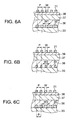
- Figs. 6A through 6C are schematic partial cross-sectional views each showing the positional relationship between another surface acoustic wave element and the layer thickness adjusting films.
- Figs. 7A through 7D are schematic cross-sectional views for explaining a method of manufacturing the surface acoustic wave device.
- Fig. 1 is a schematic plan view showing a surface acoustic wave device according to an embodiment of the invention.
- a surface acoustic wave device 1 is provided with an IC region 10 and a surface acoustic wave element region 20 in a semiconductor substrate.
- a semiconductor element shown in Fig. 2
- Al wiring 11 for connecting the semiconductor element is stacked thereon.
- Al pads 12 are provided for electrical connection with the outside.
- a high-frequency circuit such as an oscillator circuit for driving the surface acoustic wave element 24 is included in the IC region 10.
- the semiconductor substrate is equipped with the IC region 10 and the surface acoustic wave element region 20 to configure the surface acoustic wave device 1 as a single chip.
- Fig. 2 is a schematic partial cross-sectional view along the A-A line in the surface acoustic wave device 1 shown in Fig. 1 .
- the IC region 10 on the semiconductor substrate 30 made of silicon there are formed a large number of semiconductor elements 31 using a known method.
- the surface acoustic wave element region 20 on the semiconductor substrate 30 there is formed first layer thickness adjusting films 32 made of A1.
- an element insulating film 33 made of SiO 2 is formed on the semiconductor elements 31 and the first layer thickness adjusting films 32 to insulate the semiconductor elements 31.
- a semiconductor element layer 40 composed of the semiconductor elements 31 and the element insulating film 33 is formed in the IC region 10.
- A1 wiring 11 for connecting the semiconductor 31, and on the element insulating film 33 in the surface acoustic wave element region 20, there are formed second layer thickness adjusting films 35.
- the second layer thickness adjusting films 35 are provided using the same processes as the A1 wiring 11, and are formed to have the same thickness as the Al wiring 11.
- a wiring insulating film 36 made of SiO 2 is formed on the Al wiring 11.
- a wiring layer 41 composed of the Al wiring 11 and the wiring insulating film 36 is formed in the IC region 10.
- a moisture resistant film 37 made of Si 3 N 4 is formed on the wiring insulating film 36, and a piezoelectric thin film 38 made of ZnO is formed on the moisture resistant film 37. Further, on the piezoelectric thin film 38 in the surface acoustic wave element 20, there is formed a surface acoustic wave element 24 made of Al.
- Fig. 3 is a schematic cross-sectional view along the B-B cutting line in Fig. 1
- Fig. 4 is a schematic plan view for showing a layout pattern of a set of the layer thickness adjusting films.
- the first layer thickness adjusting films 32 formed on the semiconductor substrate 30 are disposed on the surface acoustic wave element region 20, for example.
- the first layer thickness adjusting films 32 are formed linearly and substantially in parallel to the electrode fingers of the IDT electrode.
- the second layer thickness adjusting films 35 are also disposed in the same shape as described above.
- the IDT electrodes 22 are equipped with the electrode fingers 21, and the electrode fingers 21 are formed in series with a pitch P. Further, electrodes 26 of the reflectors 23 are also formed in the pitch P, thus forming the surface acoustic wave element 24 to have the shape having the electrodes aligned in series with the pitch P. And, the electrode fingers 21 and the electrodes 26 of the reflectors 23 are formed to have the same line width W.
- the first layer thickness adjusting films 32 and the second layer thickness adjusting films 35 are formed to have the same pitch P as that of the electrode fingers 21 with respect to the positions having the same center lines of the respective electrode fingers 21 in the width direction. Further, the width W of each of the first layer thickness adjusting films 32 and the second layer thickness adjusting films 35 is formed to be the same as the width W of each of the electrode fingers 21. Note that, the area in which the first layer thickness adjusting films 32 and the second layer thickness adjusting films 35 are formed is formed to be equal to or wider than the area in which the surface acoustic wave element 24 is formed.
- the step between the IC region 10 with the multi-layered structure and the surface acoustic wave element region 20 can be reduced by appropriately forming the layer thickness adjusting films having the same shapes as described above on the wiring insulating film.
- the step between the IC region 10 and the surface acoustic wave element region 20 can be reduced.
- the step inclines and advances to the surface acoustic wave element region 20 while the layers such as an insulating layer are stacked in the surface acoustic wave element region 20, thus ensuring evenness of the surface acoustic wave element region 20.
- the surface acoustic wave element 24 can be formed with high dimensional accuracy in the surface acoustic wave element region 20 whose evenness is ensured, thus the surface acoustic wave element 24 having superior characteristics can be obtained.
- the layer thickness adjusting films are provided so as to traverse the electrode fingers 21 of the IDT electrodes 22, interference or scattering is caused in the surface acoustic wave to attenuate the surface acoustic wave, thus making it difficult to obtain the superior characteristics. Therefore, in the present embodiment, diffused reflection of the surface acoustic wave proceeding in the depth direction can be prevented by providing the first layer thickness adjusting films 32 and the second layer thickness adjusting films 35 substantially in parallel to the electrode fingers 21 of the IDT electrodes 22 with the same pitch.
- the surface acoustic wave element 24 having superior characteristics can be formed, thus providing the surface acoustic wave device 1 having superior characteristics.
- Figs. 5A and 5B are schematic plan views each showing a modified example of the layout pattern of the set of the layer thickness adjusting films.
- layer thickness adjusting film 50 formed as a pattern composed of discontinuous lines can also be adopted.
- the first layer thickness adjusting films 50 to be formed in the surface acoustic wave element region 20 of the semiconductor substrate 30 are formed so that each of the layer thickness adjusting films is divided into pieces.
- the interval sections are preferably formed so that each of the interval sections is not continued to another one of the interval sections of the adjacent layer thickness adjusting film. According to this arrangement, the layer thickness adjusting films can more easily be formed, and freedom of designing the layer thickness adjusting films can be increased.
- layer thickness adjusting films 51 having the same pattern as the surface acoustic wave element can also be adopted.
- the photo mask used for forming the surface acoustic wave element can be shared.
- Figs. 6A through 6C are schematic partial cross-sectional views each showing a modified example of the line width of the layer thickness adjusting films and the positional relationship with the surface acoustic wave element.
- the layer thickness adjusting films can be formed to have the line width W1 wider than the line width W of the electrode fingers 21.
- the second layer thickness adjusting films 35 are formed in the same pitch P as the electrode fingers 21 with respect to the positions having the same center lines as the electrode fingers 21 in the direction of the width W, and for example the layer thickness adjusting films are formed to have the line width W1 wider than the line width W of the electrode fingers 21.
- the layer thickness adjusting films can be formed to have the line width W2 narrower than the line width W of the electrode fingers 21.
- the second layer thickness adjusting films 35 are formed in the same pitch P as the electrode fingers 21 with respect to the positions having the same center lines as the electrode fingers 21 in the direction of the width W, and the layer thickness adjusting films may be formed to have the line width W2 narrower than the line width W of the electrode fingers 21.
- the layer thickness adjusting films can also be formed to have the same pitch P as the electrode fingers 21, different center lines from those of the electrode fingers 21 in the direction of the width W, and the line width W3 including the line width W of the electrode fingers 21.
- the second layer thickness adjusting films 35 are formed with the same pitch P as the electrode fingers 21, and the layer thickness adjusting films 35 having the width W3 are disposed in the positions including the respective electrode fingers 21 and have different center lines from those of the electrode fingers 21 in the direction of the width W. Therefore, the layer thickness adjusting films 35 are formed to have the width W3 wider than the width W of the electrode fingers 21.
- the structure described above can commonly be adopted to the first layer thickness adjusting films, and the surface acoustic wave proceeding to the depth of about one wavelength can be prevented from being diffusely reflected.
- the present embodiment is described taking the case provided with the moisture resistant film 37 as an example, it can be implemented without the moisture resistant film 37 depending on the package or the use environment of the surface acoustic wave device 1.
- a CMP (Chemical Mechanical Polishing) process can be executed after forming the wiring insulating film 36 or the moisture resistant film 37 to obtain evenness with better precision.
- the evenness with good precision can also be obtained by using glass coated by a spin-coating process (Spin On Glass (hereinafter referred to as SOG)) as the element insulating film 33.
- the surface acoustic wave element 24 can be electromagnetically shielded.
- FIGs. 7A through 7D are views for explaining processes showing a method of manufacturing the surface acoustic wave device according to an embodiment of the invention, and the processes proceed in the order from 7A to 7D.
- a large number of semiconductor elements 31 are formed in the IC region 10 on the semiconductor substrate 30 made of silicon.
- the first layer thickness adjusting films 32 made of Al are formed in the surface acoustic wave element region 20 on the semiconductor substrate 30.
- the first layer thickness adjusting films 32 are formed linearly and substantially in parallel to the electrode fingers of the IDT electrode of the surface acoustic wave element, as shown in Fig. 4 .
- the first layer thickness adjusting films 32 are formed to have the same pitch and the same line width as the electrode fingers of the IDT electrode.
- the element insulating film 33 made of SiO 2 is formed on the semiconductor substrate 30 to insulate the semiconductor element 31.
- the element insulating film 33 is formed not only in the IC region 10 but also in the surface acoustic wave element region 20.
- a semiconductor element layer 40 composed of the semiconductor elements 31 and the element insulating film 33 is formed in the IC region 10.
- a part of the element insulating film 33 on the semiconductor element 31 in the IC region 10 is removed by etching to form an opening, and then the opening is filled with A1 to form the Al wiring 11 electrically connected to the semiconductor element 31.
- the second layer thickness adjusting films 35 are formed in the surface acoustic wave element region 20 together with the Al wiring 11.
- the second layer thickness adjusting films 35 are formed linearly and substantially in parallel to the electrode fingers of the IDT electrode of the surface acoustic wave element, similarly to the first layer thickness adjusting films 32.
- the wiring insulating film 36 made of SiO 2 is formed in both the IC region 10 and the surface acoustic wave element region 20 to insulate the Al wiring 11.
- a wiring layer 41 composed of the Al wiring 11 and the wiring insulating film 36 is formed in the IC region 10.
- the moisture resistant film 37 made of Si 3 N 4 is formed in both the IC region 10 and the surface acoustic wave element region 20, thus moisture resistant property of the IC can be enhanced.
- the piezoelectric thin film 38 made of ZnO is formed on the moisture resistant film 37 in both the IC region 10 and the surface acoustic wave element region 20.
- the surface acoustic wave element 24 is formed on the piezoelectric thin film 38 in the surface acoustic wave element region 20.
- the surface acoustic wave element 24 is formed as a SAW resonator equipped with the IDT electrodes 22 and the reflectors 23 shown in Fig. 1 .
- the semiconductor substrate 30 is equipped with the IC region 10 and the surface acoustic wave element region 20, thus the surface acoustic wave device 1 configured as a single chip can be obtained.
- the step between the IC region 10 with the multi-layered structure and the surface acoustic wave element region 20 can be reduced by appropriately forming the layer thickness adjusting films having the same shapes as described above on the wiring insulating film.
- the layout pattern of the layer thickness adjusting films the layout patterns described in the modified examples of the first embodiment can also be provided.
- the step between the IC region 10 and the surface acoustic wave element region 20 can be reduced.
- the surface acoustic wave element 24 can be formed with high dimensional accuracy in the surface acoustic wave element region 20 whose evenness is ensured, thus the surface acoustic wave element 24 having superior characteristics can be obtained.
- the surface acoustic wave excited by the IDT electrodes 22 proceeds to the depth of about one wavelength, the surface acoustic wave proceeding in the depth direction can be prevented from being diffusely reflected by providing the first layer thickness adjusting films 32 and the second layer thickness adjusting films 35 in the same pitch as the electrode fingers 21 of the IDT electrodes 22.
- the surface acoustic wave element 24 having superior characteristics can be formed, thus making it possible to provide the surface acoustic wave device 1 having superior characteristics.
- the element insulating film 33 shown in Fig. 2 or Fig. 7B is often formed using a vapor phase process in response to a higher frequency or finer pitch wiring.
- the previous-generation wiring of no smaller than 0.35 ⁇ m can be adopted.
- SOG SOG
- liquid glass is deposited on a wafer by spin-coating in a preliminary rotational speed of 300rpm for 3 seconds, and then in a main rotational speed of 3000rpm for 10 seconds. After then, it is processed in a baking oven at 80°C for 3 minutes, and finally cured at 300°C for 60 minutes to be completed.
- the surface acoustic wave element 24 having superior characteristics can be formed, thus making it possible to provide the surface acoustic wave device 1 having superior characteristics at a low price.
Landscapes
- Physics & Mathematics (AREA)
- Acoustics & Sound (AREA)
- Engineering & Computer Science (AREA)
- Manufacturing & Machinery (AREA)
- Surface Acoustic Wave Elements And Circuit Networks Thereof (AREA)
Claims (7)
- Oberflächenschallwellenvorrichtung, die zumindest einen IC-Bereich (10) und einen auf einem Halbleitersubstrat (30) ausgebildeten Oberflächenschallwellenelementbereich (20) enthält, als einzelnen Chip, umfassend:im IC-Bereich zumindesteine Halbleiterelementschicht (40) mit einem Halbleiterelement (30) und einem Elementisolationsfilm (33), der zum Abdecken des Halbleiterelements und des Oberflächenschallwellenelementbereichs ausgebildet ist;eine Verdrahtungsschicht (41), die durch Stapeln, auf der Halbleiterelementschicht (40), von Verdrahtung (11) zum Herstellen einer Verbindung mit dem Halbleiterelement (31) und eines Verdrahtungsisolationsfilms (36) zum Isolieren der Verdrahtung (11) ausgebildet ist, und die sich zum Oberflächenschallwellenelementbereich erstreckt; undeinen piezoelektrischen Dünnfilm (38), der über dem Verdrahtungsisolationsfilm ausgebildet ist; undim Oberflächenschallwellenelementbereich (20)ein auf dem piezoelektrischen Dünnfilm (38) ausgebildetes und mit einer, mit einer Mehrzahl von Elektrodenfingern (21) versehenen IDT-Elektrode (22) ausgestattetes Oberflächenschallwellenelement (24); undzumindest eine Schicht von Schichtdickeneinstellfilmen (32, 35);wobei die Vorrichtung dadurch gekennzeichnet ist, dass:die Dickeneinstellfilme lineare Formen aufweisen und parallel zu und mit demselben Abstand wie die Elektrodenfinger (21) der IDT-Elektrode (22) angeordnet sind, und über dem Halbleitersubstrat (30), dem Elementisolationsfilm (33) oder dem Verdrahtungsisolationsfilm (36) und unter einer Fläche ausgebildet sind, in welcher das Oberflächenschallwellenelement (24) ausgebildet ist, wobei die Schichtdickeneinstellfilme die Gleichförmigkeit des Oberflächenschallwellenelementbereichs sicherstellen und in Bezug auf die Elektrodenfinger (21) an Positionen gebildet sind, wo die Mittellinien der Elektrodenfinger in Leitungsbreitenrichtung zu den entsprechenden Mittellinien der Schichtdickeneinstellfilme in Leitungsbreitenrichtung passen.
- Oberflächenschallwellenvorrichtung gemäß Anspruch 1, wobei die Breite jeder der Elektrodenfinger (21) gleich der Breite eines entsprechenden der Schichtdickeneinstellfilme (32, 35) ist.
- Oberflächenschallwellenvorrichtung gemäß Anspruch 1, wobei jeder der Schichtdickeneinstellfilme (50) eine aus diskontinuierlichen Linien zusammengesetzte Form aufweist.
- Oberflächenschallwellenvorrichtung gemäß Anspruch 1, weiterhin umfassend einen feuchtigkeitsresistenten Film (37), der zwischen dem Verdrahtungsisolationsfilm und dem piezoelektrischen Dünnfilm ausgebildet ist.
- Verfahren zur Herstellung einer Oberflächenschallwellenvorrichtung, die zumindest einen IC-Bereich (10) und einen auf einem Halbleitersubstrat (30) ausgebildeten Schallwellenelementbereich (20) enthält, als ein einzelner Chip, umfassend:(a) Ausbilden, im IC-Bereich des Halbleitersubstrats, einer Halbleiterelementschicht (40), wobei Schritt (a) enthält:(a1) Bereitstellen eines Halbleiterelementes (31); und(a2) Bereitstellen eines Elementisolationsfilms (33), der das Halbleiterelement abdeckt;(b) Ausbilden, auf der Halbleiterelementschicht (40), einer Verdrahtungsschicht (41), wobei der Schritt (b) beinhaltet:(b1) Bereitstellen von Verdrahtung (11) zum Herstellen von Verbindung zum Halbleiterelement (31); und(b2) Bereitstellen eines Verdrahtungsisolationsfilms (36) zum Isolieren der Verdrahtung (11), der auf der Verdrahtung gestapelt ist;wobei der Schritt (a2) das Ausbilden, im Oberflächenschallwellenelementbereich, des Elementisolationsfilms (33), der die Halbleiterelementschicht bildet, beinhaltet, und der Schritt (b2) das Ausbilden, im Oberflächenschallwellenelementbereich, des Verdrahtungsisolationsfilms (36), der die Verdrahtungsschicht bildet, in einer gestapelten Weise, beinhaltet;(c) Ausbilden eines piezoelektrischen Dünnfilms (38) über dem Verdrahtungsisolationsfilm (36) im Oberflächenschallwellenelementbereich;(d) Ausbilden eines Oberflächenschallwellenelementes (24), das mit einer IDT-Elektrode (22) ausgestattet ist, auf dem piezoelektrischen Dünnfilm (38) im Oberflächenschallwellenelementbereich; und(e) Ausbilden zumindest einer Schicht an Schichtdickeneinstellfilmen (32, 35); wobei das Verfahren dadurch gekennzeichnet ist, dass:die Dickeneinstellfilme (32, 35) lineare Formen aufweisen und parallel zu und mit demselben Abstand wie Elektrodenfinger (21) der EDT-Elektrode (32) über dem Halbleitersubstrat (30), dem Elementisolationsfilm (33) oder dem Verdrahtungsisolationsfilm (36) und unterhalb eines Bereichs angeordnet sind, in dem das Oberflächenschallwellenelement (24) ausgebildet wird, wodurch die Gleichförmigkeit des Oberflächenschallwellenelementbereichs sichergestellt wird; undsie in Bezug auf die Elektrodenfinger (21) an Positionen ausgebildet sind, wo die Mittellinien der Elektrodenfinger in Leitungsbreitenrichtung zu entsprechenden Mittellinien der Schichtdickeneinstellfilme in Leitungsbreitenrichtung passen.
- Verfahren zur Herstellung einer Oberflächenschallwellenvorrichtung gemäß Anspruch 5, wobei Schritt (b1) und Schritt (e) gleichzeitig ausgeführt werden, um die Schichtdickeneinstellfilme (35) mit der Verdrahtung in derselben Schicht auszubilden.
- Verfahren zur Herstellung einer Oberflächenschallwellenvorrichtung gemäß Anspruch 5, weiterhin umfassend:(f) Ausbilden eines feuchtigkeitsresistenten Films (37) zwischen dem Verdrahtungsisolationsfilm und dem piezoelektrischen Dünnfilm.
Applications Claiming Priority (2)
| Application Number | Priority Date | Filing Date | Title |
|---|---|---|---|
| JP2004368866 | 2004-12-21 | ||
| JP2005247275A JP4033205B2 (ja) | 2004-12-21 | 2005-08-29 | 弾性表面波装置及び弾性表面波装置の製造方法 |
Publications (2)
| Publication Number | Publication Date |
|---|---|
| EP1675261A1 EP1675261A1 (de) | 2006-06-28 |
| EP1675261B1 true EP1675261B1 (de) | 2008-12-31 |
Family
ID=36011122
Family Applications (1)
| Application Number | Title | Priority Date | Filing Date |
|---|---|---|---|
| EP20050027864 Expired - Fee Related EP1675261B1 (de) | 2004-12-21 | 2005-12-20 | SAW Bauelement und Herstellungsmethode für ein SAW Bauelement |
Country Status (5)
| Country | Link |
|---|---|
| US (1) | US7400219B2 (de) |
| EP (1) | EP1675261B1 (de) |
| JP (1) | JP4033205B2 (de) |
| KR (1) | KR20060071354A (de) |
| DE (1) | DE602005012044D1 (de) |
Families Citing this family (9)
| Publication number | Priority date | Publication date | Assignee | Title |
|---|---|---|---|---|
| JP4033204B2 (ja) * | 2004-12-01 | 2008-01-16 | セイコーエプソン株式会社 | 弾性表面波素子の製造方法 |
| US20100007444A1 (en) * | 2006-04-20 | 2010-01-14 | Anis Nurashikin Nordin | GHz Surface Acoustic Resonators in RF-CMOS |
| US8143681B2 (en) * | 2006-04-20 | 2012-03-27 | The George Washington University | Saw devices, processes for making them, and methods of use |
| US7394164B2 (en) * | 2006-07-28 | 2008-07-01 | Ultra Chip, Inc. | Semiconductor device having bumps in a same row for staggered probing |
| US8018010B2 (en) * | 2007-04-20 | 2011-09-13 | The George Washington University | Circular surface acoustic wave (SAW) devices, processes for making them, and methods of use |
| US20090124513A1 (en) * | 2007-04-20 | 2009-05-14 | Patricia Berg | Multiplex Biosensor |
| CN101788520A (zh) * | 2010-03-16 | 2010-07-28 | 浙江大学 | 含硅聚电解质声表面波谐振型湿敏元件及其制备方法 |
| US8960004B2 (en) | 2010-09-29 | 2015-02-24 | The George Washington University | Synchronous one-pole surface acoustic wave resonator |
| US20140342471A1 (en) * | 2013-05-20 | 2014-11-20 | Varian Semiconductor Equipment Associates, Inc. | Variable Doping Of Solar Cells |
Family Cites Families (10)
| Publication number | Priority date | Publication date | Assignee | Title |
|---|---|---|---|---|
| JPS58139518A (ja) | 1982-02-15 | 1983-08-18 | Showa Electric Wire & Cable Co Ltd | 薄膜弾性表面波装置 |
| JPS6194409A (ja) | 1984-10-15 | 1986-05-13 | Clarion Co Ltd | 弾性表面波素子の素子分離構造 |
| DE4213800A1 (de) * | 1992-04-27 | 1993-10-28 | Siemens Ag | Gewichteter Reflektor für eine Oberflächenwellenanordnung |
| JP3161831B2 (ja) | 1992-09-09 | 2001-04-25 | 株式会社日立製作所 | 回路素子モジュール |
| JPH1168496A (ja) | 1997-08-11 | 1999-03-09 | Toyo Commun Equip Co Ltd | 弾性表面波デバイスの構造及び製造方法 |
| JPH11330899A (ja) | 1998-05-19 | 1999-11-30 | Matsushita Electric Ind Co Ltd | Sawデバイスおよびその製造方法 |
| KR100316383B1 (ko) * | 1998-10-30 | 2002-02-19 | 윤덕용 | 모노리딕직접회로위에박막또는후막단결정압전소자를집적한단일칩라디오구조및그제조방법 |
| JP2000183688A (ja) | 1998-12-18 | 2000-06-30 | Kenwood Corp | 表面弾性波フイルタおよび表面弾性波フイルタの製造方法 |
| JP4103421B2 (ja) * | 2001-03-28 | 2008-06-18 | セイコーエプソン株式会社 | 電子デバイス及び電子機器 |
| JP2004221475A (ja) * | 2003-01-17 | 2004-08-05 | Mitsubishi Electric Corp | 誘導素子 |
-
2005
- 2005-08-29 JP JP2005247275A patent/JP4033205B2/ja not_active Expired - Fee Related
- 2005-12-01 US US11/290,570 patent/US7400219B2/en not_active Expired - Fee Related
- 2005-12-20 EP EP20050027864 patent/EP1675261B1/de not_active Expired - Fee Related
- 2005-12-20 DE DE200560012044 patent/DE602005012044D1/de not_active Expired - Lifetime
- 2005-12-21 KR KR20050127002A patent/KR20060071354A/ko not_active Ceased
Also Published As
| Publication number | Publication date |
|---|---|
| JP4033205B2 (ja) | 2008-01-16 |
| US7400219B2 (en) | 2008-07-15 |
| JP2006203853A (ja) | 2006-08-03 |
| EP1675261A1 (de) | 2006-06-28 |
| DE602005012044D1 (de) | 2009-02-12 |
| US20060131993A1 (en) | 2006-06-22 |
| KR20060071354A (ko) | 2006-06-26 |
Similar Documents
| Publication | Publication Date | Title |
|---|---|---|
| US9252732B2 (en) | Acoustic wave device and method for manufacturing the same | |
| CN101521493B (zh) | 电子部件及其制造方法 | |
| EP1675261B1 (de) | SAW Bauelement und Herstellungsmethode für ein SAW Bauelement | |
| US6946320B2 (en) | FBAR based duplexer device and manufacturing method thereof | |
| US11776947B2 (en) | Electronic component and manufacturing method therefor | |
| US7301423B2 (en) | Surface acoustic wave element and manufacturing method thereof | |
| US11177789B2 (en) | Acoustic wave device and method of manufacturing the same | |
| US7420441B2 (en) | Method of manufacturing monolithic surface acoustic wave device and integrated circuit | |
| CN114978093B (zh) | 声波谐振器、滤波器、通信设备及其制造方法 | |
| US7489036B2 (en) | Thin-film device | |
| US20070007664A1 (en) | Semiconductor package with molded back side and method of fabricating the same | |
| CN114631262B (zh) | Baw谐振器布置及制造方法 | |
| JP5185004B2 (ja) | 弾性境界波デバイスおよびその製造方法、デュープレクサの製造方法 | |
| US8618621B2 (en) | Semiconductor device layer structure and method of fabrication | |
| CN100505532C (zh) | 表面声波装置的制造方法及表面声波装置 | |
| US20230216477A1 (en) | Acoustic wave device and acoustic wave module | |
| US7649251B2 (en) | Thin-film device | |
| JP2026004153A (ja) | 弾性波デバイス、及びその製造方法 | |
| CN100474769C (zh) | 表面声波器件和表面声波器件的制造方法 | |
| JP2025179936A (ja) | 弾性波デバイス | |
| JP2026060038A (ja) | 弾性波デバイスを備えたモジュール、及びその製造方法 | |
| WO2023157798A1 (ja) | 弾性波装置 | |
| WO2006126756A1 (en) | Integrated passive device chip and method of manufacturing the same | |
| JP2020080384A (ja) | チップコンデンサおよびチップコンデンサの製造方法 |
Legal Events
| Date | Code | Title | Description |
|---|---|---|---|
| PUAI | Public reference made under article 153(3) epc to a published international application that has entered the european phase |
Free format text: ORIGINAL CODE: 0009012 |
|
| AK | Designated contracting states |
Kind code of ref document: A1 Designated state(s): AT BE BG CH CY CZ DE DK EE ES FI FR GB GR HU IE IS IT LI LT LU LV MC NL PL PT RO SE SI SK TR |
|
| AX | Request for extension of the european patent |
Extension state: AL BA HR MK YU |
|
| 17P | Request for examination filed |
Effective date: 20060724 |
|
| 17Q | First examination report despatched |
Effective date: 20060828 |
|
| AKX | Designation fees paid |
Designated state(s): DE FR |
|
| GRAP | Despatch of communication of intention to grant a patent |
Free format text: ORIGINAL CODE: EPIDOSNIGR1 |
|
| GRAS | Grant fee paid |
Free format text: ORIGINAL CODE: EPIDOSNIGR3 |
|
| GRAA | (expected) grant |
Free format text: ORIGINAL CODE: 0009210 |
|
| AK | Designated contracting states |
Kind code of ref document: B1 Designated state(s): DE FR |
|
| REF | Corresponds to: |
Ref document number: 602005012044 Country of ref document: DE Date of ref document: 20090212 Kind code of ref document: P |
|
| PLBE | No opposition filed within time limit |
Free format text: ORIGINAL CODE: 0009261 |
|
| STAA | Information on the status of an ep patent application or granted ep patent |
Free format text: STATUS: NO OPPOSITION FILED WITHIN TIME LIMIT |
|
| 26N | No opposition filed |
Effective date: 20091001 |
|
| PGFP | Annual fee paid to national office [announced via postgrant information from national office to epo] |
Ref country code: DE Payment date: 20121213 Year of fee payment: 8 |
|
| PGFP | Annual fee paid to national office [announced via postgrant information from national office to epo] |
Ref country code: FR Payment date: 20130107 Year of fee payment: 8 |
|
| REG | Reference to a national code |
Ref country code: DE Ref legal event code: R119 Ref document number: 602005012044 Country of ref document: DE |
|
| REG | Reference to a national code |
Ref country code: FR Ref legal event code: ST Effective date: 20140829 |
|
| REG | Reference to a national code |
Ref country code: DE Ref legal event code: R119 Ref document number: 602005012044 Country of ref document: DE Effective date: 20140701 |
|
| PG25 | Lapsed in a contracting state [announced via postgrant information from national office to epo] |
Ref country code: DE Free format text: LAPSE BECAUSE OF NON-PAYMENT OF DUE FEES Effective date: 20140701 |
|
| PG25 | Lapsed in a contracting state [announced via postgrant information from national office to epo] |
Ref country code: FR Free format text: LAPSE BECAUSE OF NON-PAYMENT OF DUE FEES Effective date: 20131231 |