EP1675182A2 - Image sensor pixel having a transfer gate formed from P+ or N+ doped polysilicon - Google Patents
Image sensor pixel having a transfer gate formed from P+ or N+ doped polysilicon Download PDFInfo
- Publication number
- EP1675182A2 EP1675182A2 EP05257094A EP05257094A EP1675182A2 EP 1675182 A2 EP1675182 A2 EP 1675182A2 EP 05257094 A EP05257094 A EP 05257094A EP 05257094 A EP05257094 A EP 05257094A EP 1675182 A2 EP1675182 A2 EP 1675182A2
- Authority
- EP
- European Patent Office
- Prior art keywords
- pixel
- transfer gate
- floating node
- doped
- semiconductor substrate
- Prior art date
- Legal status (The legal status is an assumption and is not a legal conclusion. Google has not performed a legal analysis and makes no representation as to the accuracy of the status listed.)
- Granted
Links
Images

Classifications
-
- H—ELECTRICITY
- H10—SEMICONDUCTOR DEVICES; ELECTRIC SOLID-STATE DEVICES NOT OTHERWISE PROVIDED FOR
- H10F—INORGANIC SEMICONDUCTOR DEVICES SENSITIVE TO INFRARED RADIATION, LIGHT, ELECTROMAGNETIC RADIATION OF SHORTER WAVELENGTH OR CORPUSCULAR RADIATION
- H10F39/00—Integrated devices, or assemblies of multiple devices, comprising at least one element covered by group H10F30/00, e.g. radiation detectors comprising photodiode arrays
- H10F39/011—Manufacture or treatment of image sensors covered by group H10F39/12
- H10F39/014—Manufacture or treatment of image sensors covered by group H10F39/12 of CMOS image sensors
-
- H—ELECTRICITY
- H10—SEMICONDUCTOR DEVICES; ELECTRIC SOLID-STATE DEVICES NOT OTHERWISE PROVIDED FOR
- H10F—INORGANIC SEMICONDUCTOR DEVICES SENSITIVE TO INFRARED RADIATION, LIGHT, ELECTROMAGNETIC RADIATION OF SHORTER WAVELENGTH OR CORPUSCULAR RADIATION
- H10F39/00—Integrated devices, or assemblies of multiple devices, comprising at least one element covered by group H10F30/00, e.g. radiation detectors comprising photodiode arrays
- H10F39/10—Integrated devices
- H10F39/12—Image sensors
- H10F39/18—Complementary metal-oxide-semiconductor [CMOS] image sensors; Photodiode array image sensors
-
- H—ELECTRICITY
- H10—SEMICONDUCTOR DEVICES; ELECTRIC SOLID-STATE DEVICES NOT OTHERWISE PROVIDED FOR
- H10F—INORGANIC SEMICONDUCTOR DEVICES SENSITIVE TO INFRARED RADIATION, LIGHT, ELECTROMAGNETIC RADIATION OF SHORTER WAVELENGTH OR CORPUSCULAR RADIATION
- H10F39/00—Integrated devices, or assemblies of multiple devices, comprising at least one element covered by group H10F30/00, e.g. radiation detectors comprising photodiode arrays
- H10F39/80—Constructional details of image sensors
- H10F39/803—Pixels having integrated switching, control, storage or amplification elements
-
- H—ELECTRICITY
- H10—SEMICONDUCTOR DEVICES; ELECTRIC SOLID-STATE DEVICES NOT OTHERWISE PROVIDED FOR
- H10F—INORGANIC SEMICONDUCTOR DEVICES SENSITIVE TO INFRARED RADIATION, LIGHT, ELECTROMAGNETIC RADIATION OF SHORTER WAVELENGTH OR CORPUSCULAR RADIATION
- H10F39/00—Integrated devices, or assemblies of multiple devices, comprising at least one element covered by group H10F30/00, e.g. radiation detectors comprising photodiode arrays
- H10F39/80—Constructional details of image sensors
- H10F39/803—Pixels having integrated switching, control, storage or amplification elements
- H10F39/8037—Pixels having integrated switching, control, storage or amplification elements the integrated elements comprising a transistor
Definitions
- the present invention relates to image sensors, and more particularly, to an image sensor that uses pixels with a transfer gate that is formed from P+ doped polysilicon.
- Image sensors have become ubiquitous. They are widely used in digital still cameras, cellular phones, security cameras, medical, automobile, and other applications.
- the technology used to manufacture image sensors, and in particular CMOS image sensors, has continued to advance at great pace. For example, the demands of higher resolution and lower power consumption have encouraged the further miniaturization and integration of the image sensor.
- each pixel of an image sensor typically includes a photosensitive element, such as a photodiode, and one or more transistors for reading out the signal from the photosensitive element.
- the transistors are generally made smaller.
- a transfer transistor is commonly used in a pixel using a four-transistor design.
- the transfer transistor has a transfer gate formed between the photosensitive element and a floating node.
- the transfer gate is an important element in the pixel and it is desirable to scale the transfer gate to have a shorter gate length for reasons of greater integration and enhanced pixel fill factor.
- the present invention provides a pixel according to Claim 1.
- Other aspects will be apparent from the attached claims.
- Figure 1 shows a combination cross-sectional view of a prior art image sensor and active pixel that uses four transistors. This is known in the art as a 4T active pixel.
- the photodiode design of the present invention can be used with any type of pixel design, including but not limited to 5T, 6T, and other designs.
- a portion 101 of an image sensor is shown.
- the portion 101 of the image sensor includes a pixel 103, an n-channel periphery area 105, and a p-channel periphery area 107.
- the n-channel periphery area 105 and p-channel periphery area 107 contains those elements of the image sensor outside of the pixel array.
- the transistors shown in areas 105 and 107 of course are merely exemplar and these areas would normally contain many transistors (PMOS and NMOS).
- the pixel 103 is only one exemplar pixel in the pixel array.
- the pixel includes a photosensitive element 109, which in this embodiment is a pinned photodiode.
- the photosensitive element may be a photogate, photocapacitor, partially pinned photodiode, or unpinned photodiode.
- the photodiode 109 outputs a signal that is used to modulate an amplification transistor 115.
- the amplification transistor 115 is also referred to as a source follower transistor.
- a transfer transistor having a transfer gate 111 is used to transfer the signal output by the photodiode 109 to a floating node 117 (N+ doped) and the gate of the amplification transistor 115.
- the photodiode 109 In operation, during an integration period (also referred to as an exposure or accumulation period), the photodiode 109 generates charge (in response to incident light) that is held in the N - layer of the photodiode 109.
- the transfer gate 111 is turned on to transfer the charge held in the N - layer to the floating node 117.
- the transfer gate 117 is turned off again for the start of a subsequent integration period.
- the signal on the floating node 117 is then used to modulate the amplification transistor 115.
- a reset transistor having a reset gate 113 resets the floating node 117 to a reference voltage.
- the reference voltage is V dd .
- the present invention acts to reduce transfer gate leakage current without the loss of image sensor performance and with minimal increased processing/manufacturing complexity.
- the N+ regions for the floating node 117 and the connection to the reset reference voltage V dd are formed using a masking and implanting process.
- the same masking and implanting process (typically using arsenic and/or phosphorus) is used to form N+ regions for the NMOS transistors in the n-channel periphery area 105.
- the N+ implant process also implants N+ dopants into the polysilicon gates of the NMOS transistors in the n-channel periphery area 105, as well as the reset gate.
- advanced CMOS image sensors typically will include a surface p-channel process flow where the polysilicon gate material is implanted.
- the n-channel gates are implanted with an N+ dopant and the p-channel gates are implanted with P+. These implants are chosen to achieve low threshold voltage (V t ) n-channel and p-channel transistors. Further, there is typically also a buried p-channel process where the n-channel and p-channel polysilicon gates are all doped the same. Typically, this is N+ doped, either by implantation or preferably by the deposition of insitu N+ doped polysilicon using a phosphorus or arsenic containing source.
- a photoresist mask 201 is used for the N+ implant that protects the transfer gate 111 from exposure to the N+ implant.
- the transfer gate 111 was also implanted with the conventional N+ doping applied to the n-channel NMOS transistors.
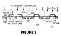
- a second photoresist mask 301 is formed.
- the second photoresist mask 301 in general leaves exposed the PMOS transistors in the p-channel periphery area 107 and the transfer gate 111.
- the polysilicon of the transfer gate 111 is also implanted with P+ dopants. This creates a transfer gate 111 that has a relatively high threshold voltage (V t ) because of the work function change of the P+ doped transfer gate 111.
- the dopant may be for example boron or BF 2 .
- boron is implanted using 500 eV - 20 KeV, and preferably between 2 KeV - 10 KeV of energy and a dopant concentration of 5e14 ions/cm 2 to 5e16 ions/cm 2 , and more preferably 1e15 ions/cm 2 to 1e16 ions/cm 2 .
- implant energies and dopant concentrations may also be used, depending upon specific desired device characteristics and other design considerations.
- the P+ doping may be done during an insitu doping process where the polysilicon layer that forms the transfer gate is formed in the presence of a boron containing substance, such as B 2 H 6 or BCl 3 .
- the process described above does not include any additional steps, but merely the adjusting of the pattern of the photoresist mask 301 for the p-channel PMOS transistor implant. As such, there is little additional complexity in implementing the present invention. Further, the leakage current (I off ) is greatly improved allowing the transfer gate 111 to be scaled to shorter gate lengths. Moreover, with a higher threshold voltage (V t ) for the transfer gate 111, the enhancement implant for the photodiode 109 and transfer transistor regions can now be reduced to provide even further improvement in the barrier/well potential at the photodiode 109 and transfer gate 111 interface.
- the p-channel transfer transistor would have its transfer gate doped with an N+ implant.
- the dopant may be for example arsenic or phosphorus.
- arsenic or phosphorus is implanted using 1 KeV - 200 KeV, and preferably between 5 KeV - 50 KeV of energy and a dopant concentration of 5e14 ions/cm 2 to 5e16 ions/cm 2 , and more preferably 1e15 ions/cm 2 to 1e16 ions/cm 2 .
- implant energies and dopant concentrations may also be used, depending upon specific desired device characteristics and other design considerations.
- the N+ doping may be done during an insitu doping process where the polysilicon layer that forms the transfer gate is formed in the presence of a n-type dopant, such as P 2 H 6 or POCl 3 or arsine.
- a n-type dopant such as P 2 H 6 or POCl 3 or arsine.
- the present invention has been discussed in the context of an image sensor transfer transistor, the present invention may also be applied to any CMOS transistor where leakage current is an issue.
Landscapes
- Solid State Image Pick-Up Elements (AREA)
- Transforming Light Signals Into Electric Signals (AREA)
Abstract
Description
- The present invention relates to image sensors, and more particularly, to an image sensor that uses pixels with a transfer gate that is formed from P+ doped polysilicon.
- Image sensors have become ubiquitous. They are widely used in digital still cameras, cellular phones, security cameras, medical, automobile, and other applications. The technology used to manufacture image sensors, and in particular CMOS image sensors, has continued to advance at great pace. For example, the demands of higher resolution and lower power consumption have encouraged the further miniaturization and integration of the image sensor.
- Typically each pixel of an image sensor includes a photosensitive element, such as a photodiode, and one or more transistors for reading out the signal from the photosensitive element. With greater integration, the transistors are generally made smaller. For example, a transfer transistor is commonly used in a pixel using a four-transistor design. The transfer transistor has a transfer gate formed between the photosensitive element and a floating node. The transfer gate is an important element in the pixel and it is desirable to scale the transfer gate to have a shorter gate length for reasons of greater integration and enhanced pixel fill factor.
- However, short gate lengths may result in leakage current from the photosensitive element to the floating node. One method of dealing with this leakage current is to increase the enhancement implant under the transfer gate. This increases the barrier/well potentials at the transfer gate and photodiode interface. The increase of the barrier/well potentials will also degrade image sensor performance by increasing image lag.
- In a first aspect, the present invention provides a pixel according to Claim 1. Other aspects will be apparent from the attached claims.
-
- Figure 1 is a cross-sectional view of a prior art four transistor (4T) pixel as well as the peripheral p-channel and n-channel transistors.
- Figures 2 and 3 are cross-sectional diagrams showing a method of making a pixel in accordance with the present invention.
- In the following description, numerous specific details are provided in order to give a thorough understanding of embodiments of the invention. One skilled in the relevant art will recognize, however, that the invention may be practiced without one or more of the specific details, or with other methods, components, materials, etc. In other instances, well known structures, materials, or operations are not shown or described in order to avoid obscuring aspects of the invention.
- Referenced throughout the specification to "one embodiment" or "an embodiment" means that a particular feature, structure, or characteristic described in connection with the embodiment and included in at least one embodiment of the present invention. Thus, the appearances of the phrase "in one embodiment" or "in an embodiment" in various places throughout the specification are not necessarily all referring to the same embodiment. Furthermore, the particular features, structures, or characteristics may be combined in any suitable manner in one or more embodiments.
- Figure 1 shows a combination cross-sectional view of a prior art image sensor and active pixel that uses four transistors. This is known in the art as a 4T active pixel. However, it can be appreciated that the photodiode design of the present invention can be used with any type of pixel design, including but not limited to 5T, 6T, and other designs.
- As seen in Figure 1, a
portion 101 of an image sensor is shown. Theportion 101 of the image sensor includes apixel 103, an n-channel periphery area 105, and a p-channel periphery area 107. The n-channel periphery area 105 and p-channel periphery area 107 contains those elements of the image sensor outside of the pixel array. The transistors shown inareas - The
pixel 103 is only one exemplar pixel in the pixel array. The pixel includes aphotosensitive element 109, which in this embodiment is a pinned photodiode. However, the photosensitive element may be a photogate, photocapacitor, partially pinned photodiode, or unpinned photodiode. - The
photodiode 109, outputs a signal that is used to modulate anamplification transistor 115. Theamplification transistor 115 is also referred to as a source follower transistor. A transfer transistor having atransfer gate 111 is used to transfer the signal output by thephotodiode 109 to a floating node 117 (N+ doped) and the gate of theamplification transistor 115. - In operation, during an integration period (also referred to as an exposure or accumulation period), the
photodiode 109 generates charge (in response to incident light) that is held in the N- layer of thephotodiode 109. After the integration period, thetransfer gate 111 is turned on to transfer the charge held in the N- layer to thefloating node 117. After the signal has been transferred to thefloating node 117, thetransfer gate 117 is turned off again for the start of a subsequent integration period. The signal on thefloating node 117 is then used to modulate theamplification transistor 115. After readout, a reset transistor having areset gate 113 resets thefloating node 117 to a reference voltage. In one embodiment, the reference voltage is Vdd. - However, as noted above, as the
transfer gate 111 decreases in size due to integration and fill factor demands, the occurrence of leakage current from thephotodiode 109 to thefloating node 117 increases. The present invention acts to reduce transfer gate leakage current without the loss of image sensor performance and with minimal increased processing/manufacturing complexity. - In that regard, the N+ regions for the
floating node 117 and the connection to the reset reference voltage Vdd are formed using a masking and implanting process. The same masking and implanting process (typically using arsenic and/or phosphorus) is used to form N+ regions for the NMOS transistors in the n-channel periphery area 105. The N+ implant process also implants N+ dopants into the polysilicon gates of the NMOS transistors in the n-channel periphery area 105, as well as the reset gate. Note that advanced CMOS image sensors typically will include a surface p-channel process flow where the polysilicon gate material is implanted. Typically, the n-channel gates are implanted with an N+ dopant and the p-channel gates are implanted with P+. These implants are chosen to achieve low threshold voltage (Vt) n-channel and p-channel transistors. Further, there is typically also a buried p-channel process where the n-channel and p-channel polysilicon gates are all doped the same. Typically, this is N+ doped, either by implantation or preferably by the deposition of insitu N+ doped polysilicon using a phosphorus or arsenic containing source. - As seen in Figure 2 of the present invention, a
photoresist mask 201 is used for the N+ implant that protects thetransfer gate 111 from exposure to the N+ implant. In the prior art, thetransfer gate 111 was also implanted with the conventional N+ doping applied to the n-channel NMOS transistors. - In accordance with the present invention, turning to Figure 3, a second
photoresist mask 301 is formed. Thesecond photoresist mask 301 in general leaves exposed the PMOS transistors in the p-channel periphery area 107 and thetransfer gate 111. Thus, as seen in Figure 3, during the implantation of the P+ dopants, the polysilicon of thetransfer gate 111 is also implanted with P+ dopants. This creates atransfer gate 111 that has a relatively high threshold voltage (Vt) because of the work function change of the P+ dopedtransfer gate 111. - The dopant may be for example boron or BF2. In one embodiment, boron is implanted using 500 eV - 20 KeV, and preferably between 2 KeV - 10 KeV of energy and a dopant concentration of 5e14 ions/cm2 to 5e16 ions/cm2, and more preferably 1e15 ions/cm2 to 1e16 ions/cm2. However, it can be appreciated that other implant energies and dopant concentrations may also be used, depending upon specific desired device characteristics and other design considerations.
- Additionally, the P+ doping may be done during an insitu doping process where the polysilicon layer that forms the transfer gate is formed in the presence of a boron containing substance, such as B2H6 or BCl3.
- It is important to note that the process described above does not include any additional steps, but merely the adjusting of the pattern of the
photoresist mask 301 for the p-channel PMOS transistor implant. As such, there is little additional complexity in implementing the present invention. Further, the leakage current (Ioff) is greatly improved allowing thetransfer gate 111 to be scaled to shorter gate lengths. Moreover, with a higher threshold voltage (Vt) for thetransfer gate 111, the enhancement implant for thephotodiode 109 and transfer transistor regions can now be reduced to provide even further improvement in the barrier/well potential at thephotodiode 109 andtransfer gate 111 interface. - While the present invention has been described in the context of an n-channel transfer transistor, the same concept can be applied to a p-channel transfer transistor. Thus, the p-channel transfer transistor would have its transfer gate doped with an N+ implant. The dopant may be for example arsenic or phosphorus. In one embodiment, arsenic or phosphorus is implanted using 1 KeV - 200 KeV, and preferably between 5 KeV - 50 KeV of energy and a dopant concentration of 5e14 ions/cm2 to 5e16 ions/cm2, and more preferably 1e15 ions/cm2 to 1e16 ions/cm2. However, it can be appreciated that other implant energies and dopant concentrations may also be used, depending upon specific desired device characteristics and other design considerations.
- Alternatively, the N+ doping may be done during an insitu doping process where the polysilicon layer that forms the transfer gate is formed in the presence of a n-type dopant, such as P2H6 or POCl3 or arsine.
- Further, although the present invention has been discussed in the context of an image sensor transfer transistor, the present invention may also be applied to any CMOS transistor where leakage current is an issue.
- Thus, from the foregoing, it will be appreciated that specific embodiments of the invention have been described herein for purposes of illustration, but that various modifications may be made without deviating from the spirit and scope of the invention. Accordingly, the invention is not limited except as by the appended claims.
Claims (24)
- A pixel comprising:a photosensitive element formed in a semiconductor substrate;an n-type floating node formed in said semiconductor substrate; andan n-channel transfer transistor having a transfer gate between said floating node and said photosensitive element, said transfer gate doped with a p-type dopant.
- The pixel of Claim 1 wherein said photosensitive element is a photodiode, partially pinned photodiode, pinned photodiode, photogate, or photocapacitor.
- The pixel of Claim 1 wherein said transfer gate is P+ doped to a dosage of between 5e14 ions/cm2 to 5e16 ions/cm2.
- The pixel of Claim 1 further including an amplification transistor controlled by said floating node.
- The pixel of Claim 1 further including a reset transistor operative to reset said floating node to a reference voltage.
- The pixel of Claim 1 wherein said pixel is a part of a 4T, 5T, 6T, or 7T architecture.
- The pixel of Claim 1 wherein said transfer gate is P+ doped using an implant energy of between 500 eV to 20 keV.
- The pixel of Claim 1 wherein said transfer gate is P+ doped using an insitu process during formation of said transfer gate.
- A pixel comprising:a photosensitive element formed in a semiconductor substrate;a p-type floating node formed in said semiconductor substrate; anda p-channel transfer transistor having a transfer gate between said floating node and said photosensitive element, said transfer gate doped with a n-type dopant.
- The pixel of Claim 9 wherein said photosensitive element is a photodiode, partially pinned photodiode, pinned photodiode, photogate, or photocapacitor.
- The pixel of Claim 9 wherein said transfer gate is N+ doped to a dosage of between 5e14 ions/cm2 to 5e16 ions/cm2.
- The pixel of Claim 9 further including an amplification transistor controlled by said floating node.
- The pixel of Claim 9 wherein said transfer gate is N+ doped using an implant energy of between 1 keV to 200 keV.
- The pixel of Claim 9 wherein said transfer gate is N+ doped using an insitu process during formation of said transfer gate.
- The pixel of Claim 9 further including a reset transistor operative to reset said floating node to a reference voltage.
- The pixel of Claim 10 wherein said pixel is a part of a 4T, 5T, 6T, or 7T architecture.
- A transistor comprising:a source region formed in a semiconductor substrate of a first conductivity type;a drain region formed in a semiconductor substrate of said first conductivity type; anda gate formed atop of said semiconductor substrate between said source and drain region, said gate doped with a second conductivity type.
- A method for forming a pixel in a semiconductor substrate comprising:forming a photosensitive element in said semiconductor substrate;forming a floating node in said semiconductor substrate, said floating node of a first conductivity type;forming a transfer transistor having a transfer gate between said photosensitive element and said floating node; anddoping said transfer gate with a second conductivity type.
- The method of Claim 18 wherein said photosensitive element is a photodiode, partially pinned photodiode, pinned photodiode, photogate, or photocapacitor.
- The method of Claim 18 wherein said transfer gate is P+ doped to a dosage of between 5e14 ions/cm2 to 5e16 ions/cm2
- The method of Claim 18 further including forming an amplification transistor controlled by said floating node.
- The method of Claim 18 wherein said first conductivity type is n-type and said second conductivity type is p-type.
- The method of Claim 18 wherein said step of doping said transfer gate is performed during a same masking step used for forming P+ regions in a p-channel periphery area of said semiconductor substrate.
- The method of Claim 18 wherein said transfer gate is masked during formation of said floating node.
Applications Claiming Priority (1)
| Application Number | Priority Date | Filing Date | Title |
|---|---|---|---|
| US11/021,134 US7675094B2 (en) | 2004-12-22 | 2004-12-22 | Image sensor pixel having a transfer gate formed from P+ or N+ doped polysilicon |
Publications (3)
| Publication Number | Publication Date |
|---|---|
| EP1675182A2 true EP1675182A2 (en) | 2006-06-28 |
| EP1675182A3 EP1675182A3 (en) | 2009-02-11 |
| EP1675182B1 EP1675182B1 (en) | 2013-02-27 |
Family
ID=36128438
Family Applications (1)
| Application Number | Title | Priority Date | Filing Date |
|---|---|---|---|
| EP05257094A Expired - Lifetime EP1675182B1 (en) | 2004-12-22 | 2005-11-17 | Image sensor pixel having a transfer gate formed from P+ or N+ doped polysilicon |
Country Status (4)
| Country | Link |
|---|---|
| US (1) | US7675094B2 (en) |
| EP (1) | EP1675182B1 (en) |
| CN (1) | CN1819238B (en) |
| TW (1) | TWI299210B (en) |
Cited By (1)
| Publication number | Priority date | Publication date | Assignee | Title |
|---|---|---|---|---|
| WO2011082118A2 (en) | 2009-12-30 | 2011-07-07 | Omnivision Technologies, Inc. | Image sensor with doped transfer gate |
Families Citing this family (4)
| Publication number | Priority date | Publication date | Assignee | Title |
|---|---|---|---|---|
| US20090261393A1 (en) * | 2008-04-18 | 2009-10-22 | United Microelectronics Corp. | Composite transfer gate and fabrication thereof |
| CN113937114A (en) * | 2020-06-29 | 2022-01-14 | 格科微电子(上海)有限公司 | Method for forming transfer transistor of CMOS image sensor |
| CN113206119B (en) * | 2021-04-29 | 2023-04-18 | 武汉新芯集成电路制造有限公司 | Active pixel circuit, image sensor, and electronic device |
| FR3152335A1 (en) * | 2023-08-21 | 2025-02-28 | Commissariat A L'energie Atomique Et Aux Energies Alternatives | Image sensor |
Citations (5)
| Publication number | Priority date | Publication date | Assignee | Title |
|---|---|---|---|---|
| JP2001196572A (en) | 2000-01-13 | 2001-07-19 | Canon Inc | Photoelectric conversion device |
| EP1139428A2 (en) | 2000-03-28 | 2001-10-04 | Kabushiki Kaisha Toshiba | Solid state imaging device having a photodiode and a MOSFET and method of manufacturing the same |
| WO2003044855A2 (en) | 2001-11-16 | 2003-05-30 | Altera Corporation | Polysilicon gate doping level variation for reduced leakage current |
| WO2004044989A1 (en) | 2002-11-12 | 2004-05-27 | Micron Technology, Inc. | Grounded gate and isolation techniques for reducing dark current in cmos image sensors |
| EP1642340A1 (en) | 2003-06-25 | 2006-04-05 | Micron Technology, Inc. | Tailoring gate work-function in image sensors |
Family Cites Families (11)
| Publication number | Priority date | Publication date | Assignee | Title |
|---|---|---|---|---|
| US4027380A (en) * | 1974-06-03 | 1977-06-07 | Fairchild Camera And Instrument Corporation | Complementary insulated gate field effect transistor structure and process for fabricating the structure |
| JPH0528053Y2 (en) | 1987-08-11 | 1993-07-19 | ||
| US5396096A (en) | 1992-10-07 | 1995-03-07 | Matsushita Electric Industrial Co., Ltd. | Semiconductor device and manufacturing method thereof |
| US6027978A (en) | 1997-01-28 | 2000-02-22 | Advanced Micro Devices, Inc. | Method of making an IGFET with a non-uniform lateral doping profile in the channel region |
| US6218691B1 (en) * | 1998-06-30 | 2001-04-17 | Hyundai Electronics Industries Co., Ltd. | Image sensor with improved dynamic range by applying negative voltage to unit pixel |
| US6165902A (en) * | 1998-11-06 | 2000-12-26 | Advanced Micro Devices, Inc. | Low resistance metal contact technology |
| US6166846A (en) * | 1998-12-30 | 2000-12-26 | Intel Corporaqtion | Through silicon modulator and method |
| US6657665B1 (en) | 1998-12-31 | 2003-12-02 | Eastman Kodak Company | Active Pixel Sensor with wired floating diffusions and shared amplifier |
| US6310366B1 (en) * | 1999-06-16 | 2001-10-30 | Micron Technology, Inc. | Retrograde well structure for a CMOS imager |
| US6501131B1 (en) | 1999-07-22 | 2002-12-31 | International Business Machines Corporation | Transistors having independently adjustable parameters |
| KR100955735B1 (en) * | 2003-04-30 | 2010-04-30 | 크로스텍 캐피탈, 엘엘씨 | Unit pixel of CMOS image sensor |
-
2004
- 2004-12-22 US US11/021,134 patent/US7675094B2/en active Active
-
2005
- 2005-11-08 TW TW094139191A patent/TWI299210B/en not_active IP Right Cessation
- 2005-11-17 EP EP05257094A patent/EP1675182B1/en not_active Expired - Lifetime
- 2005-12-22 CN CN2005101358861A patent/CN1819238B/en not_active Expired - Lifetime
Patent Citations (5)
| Publication number | Priority date | Publication date | Assignee | Title |
|---|---|---|---|---|
| JP2001196572A (en) | 2000-01-13 | 2001-07-19 | Canon Inc | Photoelectric conversion device |
| EP1139428A2 (en) | 2000-03-28 | 2001-10-04 | Kabushiki Kaisha Toshiba | Solid state imaging device having a photodiode and a MOSFET and method of manufacturing the same |
| WO2003044855A2 (en) | 2001-11-16 | 2003-05-30 | Altera Corporation | Polysilicon gate doping level variation for reduced leakage current |
| WO2004044989A1 (en) | 2002-11-12 | 2004-05-27 | Micron Technology, Inc. | Grounded gate and isolation techniques for reducing dark current in cmos image sensors |
| EP1642340A1 (en) | 2003-06-25 | 2006-04-05 | Micron Technology, Inc. | Tailoring gate work-function in image sensors |
Cited By (4)
| Publication number | Priority date | Publication date | Assignee | Title |
|---|---|---|---|---|
| WO2011082118A2 (en) | 2009-12-30 | 2011-07-07 | Omnivision Technologies, Inc. | Image sensor with doped transfer gate |
| WO2011082118A3 (en) * | 2009-12-30 | 2011-08-18 | Omnivision Technologies, Inc. | Image sensor with doped transfer gate |
| US9000500B2 (en) | 2009-12-30 | 2015-04-07 | Omnivision Technologies, Inc. | Image sensor with doped transfer gate |
| US9431456B2 (en) | 2009-12-30 | 2016-08-30 | Omnivision Technologies, Inc. | Image sensor with doped transfer gate |
Also Published As
| Publication number | Publication date |
|---|---|
| EP1675182A3 (en) | 2009-02-11 |
| EP1675182B1 (en) | 2013-02-27 |
| US20060131592A1 (en) | 2006-06-22 |
| TWI299210B (en) | 2008-07-21 |
| TW200625614A (en) | 2006-07-16 |
| US7675094B2 (en) | 2010-03-09 |
| CN1819238A (en) | 2006-08-16 |
| CN1819238B (en) | 2011-02-02 |
Similar Documents
| Publication | Publication Date | Title |
|---|---|---|
| US7154137B2 (en) | Image sensor and pixel having a non-convex photodiode | |
| US7825444B2 (en) | Image sensor pixel having a lateral doping profile formed with indium doping | |
| US7939357B2 (en) | Image sensor pixel having photodiode with multi-dopant implantation | |
| US7115925B2 (en) | Image sensor and pixel having an optimized floating diffusion | |
| US20080318358A1 (en) | Image sensor pixel having photodiode with indium pinning layer | |
| US20090212335A1 (en) | Complementary metal-oxide-semiconductor (cmos) image sensor and fabricating method thereof | |
| US11901383B2 (en) | Transistor having increased effective channel width | |
| US7541210B2 (en) | Method for fabricating CMOS image sensor | |
| KR100760913B1 (en) | CMOS image sensor and its manufacturing method | |
| US7344964B2 (en) | Image sensor with improved charge transfer efficiency and method for fabricating the same | |
| US7675094B2 (en) | Image sensor pixel having a transfer gate formed from P+ or N+ doped polysilicon | |
| EP1746656A2 (en) | Pixel sensor with raised silicon photodiode | |
| KR100494032B1 (en) | CMOS Imagesensor and fabrication method of the same | |
| KR100790213B1 (en) | Manufacturing Method of Image Sensor | |
| KR100766705B1 (en) | Image sensor and its manufacturing method | |
| KR20030037655A (en) | Method of manufacturing cmos image sensor | |
| KR20030057617A (en) | Method for fabricating image sensor |
Legal Events
| Date | Code | Title | Description |
|---|---|---|---|
| PUAI | Public reference made under article 153(3) epc to a published international application that has entered the european phase |
Free format text: ORIGINAL CODE: 0009012 |
|
| 17P | Request for examination filed |
Effective date: 20051206 |
|
| AK | Designated contracting states |
Kind code of ref document: A2 Designated state(s): AT BE BG CH CY CZ DE DK EE ES FI FR GB GR HU IE IS IT LI LT LU LV MC NL PL PT RO SE SI SK TR |
|
| AX | Request for extension of the european patent |
Extension state: AL BA HR MK YU |
|
| PUAL | Search report despatched |
Free format text: ORIGINAL CODE: 0009013 |
|
| AK | Designated contracting states |
Kind code of ref document: A3 Designated state(s): AT BE BG CH CY CZ DE DK EE ES FI FR GB GR HU IE IS IT LI LT LU LV MC NL PL PT RO SE SI SK TR |
|
| AX | Request for extension of the european patent |
Extension state: AL BA HR MK YU |
|
| 17Q | First examination report despatched |
Effective date: 20090828 |
|
| AKX | Designation fees paid |
Designated state(s): AT BE BG CH CY CZ DE DK EE ES FI FR GB GR HU IE IS IT LI LT LU LV MC NL PL PT RO SE SI SK TR |
|
| GRAP | Despatch of communication of intention to grant a patent |
Free format text: ORIGINAL CODE: EPIDOSNIGR1 |
|
| GRAS | Grant fee paid |
Free format text: ORIGINAL CODE: EPIDOSNIGR3 |
|
| GRAA | (expected) grant |
Free format text: ORIGINAL CODE: 0009210 |
|
| AK | Designated contracting states |
Kind code of ref document: B1 Designated state(s): AT BE BG CH CY CZ DE DK EE ES FI FR GB GR HU IE IS IT LI LT LU LV MC NL PL PT RO SE SI SK TR |
|
| REG | Reference to a national code |
Ref country code: GB Ref legal event code: FG4D |
|
| REG | Reference to a national code |
Ref country code: CH Ref legal event code: EP |
|
| REG | Reference to a national code |
Ref country code: AT Ref legal event code: REF Ref document number: 598893 Country of ref document: AT Kind code of ref document: T Effective date: 20130315 |
|
| REG | Reference to a national code |
Ref country code: IE Ref legal event code: FG4D |
|
| REG | Reference to a national code |
Ref country code: DE Ref legal event code: R096 Ref document number: 602005038288 Country of ref document: DE Effective date: 20130425 |
|
| REG | Reference to a national code |
Ref country code: AT Ref legal event code: MK05 Ref document number: 598893 Country of ref document: AT Kind code of ref document: T Effective date: 20130227 |
|
| REG | Reference to a national code |
Ref country code: LT Ref legal event code: MG4D |
|
| PG25 | Lapsed in a contracting state [announced via postgrant information from national office to epo] |
Ref country code: BG Free format text: LAPSE BECAUSE OF FAILURE TO SUBMIT A TRANSLATION OF THE DESCRIPTION OR TO PAY THE FEE WITHIN THE PRESCRIBED TIME-LIMIT Effective date: 20130527 Ref country code: LT Free format text: LAPSE BECAUSE OF FAILURE TO SUBMIT A TRANSLATION OF THE DESCRIPTION OR TO PAY THE FEE WITHIN THE PRESCRIBED TIME-LIMIT Effective date: 20130227 Ref country code: SE Free format text: LAPSE BECAUSE OF FAILURE TO SUBMIT A TRANSLATION OF THE DESCRIPTION OR TO PAY THE FEE WITHIN THE PRESCRIBED TIME-LIMIT Effective date: 20130227 Ref country code: AT Free format text: LAPSE BECAUSE OF FAILURE TO SUBMIT A TRANSLATION OF THE DESCRIPTION OR TO PAY THE FEE WITHIN THE PRESCRIBED TIME-LIMIT Effective date: 20130227 Ref country code: ES Free format text: LAPSE BECAUSE OF FAILURE TO SUBMIT A TRANSLATION OF THE DESCRIPTION OR TO PAY THE FEE WITHIN THE PRESCRIBED TIME-LIMIT Effective date: 20130607 Ref country code: IS Free format text: LAPSE BECAUSE OF FAILURE TO SUBMIT A TRANSLATION OF THE DESCRIPTION OR TO PAY THE FEE WITHIN THE PRESCRIBED TIME-LIMIT Effective date: 20130627 |
|
| REG | Reference to a national code |
Ref country code: NL Ref legal event code: VDEP Effective date: 20130227 |
|
| PG25 | Lapsed in a contracting state [announced via postgrant information from national office to epo] |
Ref country code: LV Free format text: LAPSE BECAUSE OF FAILURE TO SUBMIT A TRANSLATION OF THE DESCRIPTION OR TO PAY THE FEE WITHIN THE PRESCRIBED TIME-LIMIT Effective date: 20130227 Ref country code: GR Free format text: LAPSE BECAUSE OF FAILURE TO SUBMIT A TRANSLATION OF THE DESCRIPTION OR TO PAY THE FEE WITHIN THE PRESCRIBED TIME-LIMIT Effective date: 20130528 Ref country code: SI Free format text: LAPSE BECAUSE OF FAILURE TO SUBMIT A TRANSLATION OF THE DESCRIPTION OR TO PAY THE FEE WITHIN THE PRESCRIBED TIME-LIMIT Effective date: 20130227 Ref country code: PT Free format text: LAPSE BECAUSE OF FAILURE TO SUBMIT A TRANSLATION OF THE DESCRIPTION OR TO PAY THE FEE WITHIN THE PRESCRIBED TIME-LIMIT Effective date: 20130627 Ref country code: PL Free format text: LAPSE BECAUSE OF FAILURE TO SUBMIT A TRANSLATION OF THE DESCRIPTION OR TO PAY THE FEE WITHIN THE PRESCRIBED TIME-LIMIT Effective date: 20130227 Ref country code: FI Free format text: LAPSE BECAUSE OF FAILURE TO SUBMIT A TRANSLATION OF THE DESCRIPTION OR TO PAY THE FEE WITHIN THE PRESCRIBED TIME-LIMIT Effective date: 20130227 Ref country code: BE Free format text: LAPSE BECAUSE OF FAILURE TO SUBMIT A TRANSLATION OF THE DESCRIPTION OR TO PAY THE FEE WITHIN THE PRESCRIBED TIME-LIMIT Effective date: 20130227 |
|
| PG25 | Lapsed in a contracting state [announced via postgrant information from national office to epo] |
Ref country code: CZ Free format text: LAPSE BECAUSE OF FAILURE TO SUBMIT A TRANSLATION OF THE DESCRIPTION OR TO PAY THE FEE WITHIN THE PRESCRIBED TIME-LIMIT Effective date: 20130227 Ref country code: EE Free format text: LAPSE BECAUSE OF FAILURE TO SUBMIT A TRANSLATION OF THE DESCRIPTION OR TO PAY THE FEE WITHIN THE PRESCRIBED TIME-LIMIT Effective date: 20130227 Ref country code: SK Free format text: LAPSE BECAUSE OF FAILURE TO SUBMIT A TRANSLATION OF THE DESCRIPTION OR TO PAY THE FEE WITHIN THE PRESCRIBED TIME-LIMIT Effective date: 20130227 Ref country code: DK Free format text: LAPSE BECAUSE OF FAILURE TO SUBMIT A TRANSLATION OF THE DESCRIPTION OR TO PAY THE FEE WITHIN THE PRESCRIBED TIME-LIMIT Effective date: 20130227 Ref country code: RO Free format text: LAPSE BECAUSE OF FAILURE TO SUBMIT A TRANSLATION OF THE DESCRIPTION OR TO PAY THE FEE WITHIN THE PRESCRIBED TIME-LIMIT Effective date: 20130227 Ref country code: NL Free format text: LAPSE BECAUSE OF FAILURE TO SUBMIT A TRANSLATION OF THE DESCRIPTION OR TO PAY THE FEE WITHIN THE PRESCRIBED TIME-LIMIT Effective date: 20130227 |
|
| PG25 | Lapsed in a contracting state [announced via postgrant information from national office to epo] |
Ref country code: CY Free format text: LAPSE BECAUSE OF FAILURE TO SUBMIT A TRANSLATION OF THE DESCRIPTION OR TO PAY THE FEE WITHIN THE PRESCRIBED TIME-LIMIT Effective date: 20130227 |
|
| PG25 | Lapsed in a contracting state [announced via postgrant information from national office to epo] |
Ref country code: IT Free format text: LAPSE BECAUSE OF FAILURE TO SUBMIT A TRANSLATION OF THE DESCRIPTION OR TO PAY THE FEE WITHIN THE PRESCRIBED TIME-LIMIT Effective date: 20130227 |
|
| PLBE | No opposition filed within time limit |
Free format text: ORIGINAL CODE: 0009261 |
|
| STAA | Information on the status of an ep patent application or granted ep patent |
Free format text: STATUS: NO OPPOSITION FILED WITHIN TIME LIMIT |
|
| 26N | No opposition filed |
Effective date: 20131128 |
|
| REG | Reference to a national code |
Ref country code: DE Ref legal event code: R097 Ref document number: 602005038288 Country of ref document: DE Effective date: 20131128 |
|
| PG25 | Lapsed in a contracting state [announced via postgrant information from national office to epo] |
Ref country code: MC Free format text: LAPSE BECAUSE OF FAILURE TO SUBMIT A TRANSLATION OF THE DESCRIPTION OR TO PAY THE FEE WITHIN THE PRESCRIBED TIME-LIMIT Effective date: 20130227 |
|
| REG | Reference to a national code |
Ref country code: IE Ref legal event code: MM4A |
|
| PG25 | Lapsed in a contracting state [announced via postgrant information from national office to epo] |
Ref country code: IE Free format text: LAPSE BECAUSE OF NON-PAYMENT OF DUE FEES Effective date: 20131117 |
|
| PG25 | Lapsed in a contracting state [announced via postgrant information from national office to epo] |
Ref country code: TR Free format text: LAPSE BECAUSE OF FAILURE TO SUBMIT A TRANSLATION OF THE DESCRIPTION OR TO PAY THE FEE WITHIN THE PRESCRIBED TIME-LIMIT Effective date: 20130227 |
|
| PG25 | Lapsed in a contracting state [announced via postgrant information from national office to epo] |
Ref country code: HU Free format text: LAPSE BECAUSE OF FAILURE TO SUBMIT A TRANSLATION OF THE DESCRIPTION OR TO PAY THE FEE WITHIN THE PRESCRIBED TIME-LIMIT; INVALID AB INITIO Effective date: 20051117 Ref country code: LU Free format text: LAPSE BECAUSE OF NON-PAYMENT OF DUE FEES Effective date: 20131117 |
|
| REG | Reference to a national code |
Ref country code: FR Ref legal event code: PLFP Year of fee payment: 11 |
|
| REG | Reference to a national code |
Ref country code: FR Ref legal event code: PLFP Year of fee payment: 12 |
|
| REG | Reference to a national code |
Ref country code: FR Ref legal event code: PLFP Year of fee payment: 13 |
|
| REG | Reference to a national code |
Ref country code: FR Ref legal event code: PLFP Year of fee payment: 14 |
|
| REG | Reference to a national code |
Ref country code: DE Ref legal event code: R079 Ref document number: 602005038288 Country of ref document: DE Free format text: PREVIOUS MAIN CLASS: H01L0027146000 Ipc: H10F0039180000 |
|
| PGFP | Annual fee paid to national office [announced via postgrant information from national office to epo] |
Ref country code: DE Payment date: 20241010 Year of fee payment: 20 |
|
| PGFP | Annual fee paid to national office [announced via postgrant information from national office to epo] |
Ref country code: GB Payment date: 20241010 Year of fee payment: 20 |
|
| PGFP | Annual fee paid to national office [announced via postgrant information from national office to epo] |
Ref country code: FR Payment date: 20241010 Year of fee payment: 20 |
|
| PGFP | Annual fee paid to national office [announced via postgrant information from national office to epo] |
Ref country code: CH Payment date: 20241201 Year of fee payment: 20 |
|
| REG | Reference to a national code |
Ref country code: CH Ref legal event code: H14 Free format text: ST27 STATUS EVENT CODE: U-0-0-H10-H14 (AS PROVIDED BY THE NATIONAL OFFICE) Effective date: 20251117 Ref country code: DE Ref legal event code: R071 Ref document number: 602005038288 Country of ref document: DE |
|
| REG | Reference to a national code |
Ref country code: GB Ref legal event code: PE20 Expiry date: 20251116 |