EP1675163A2 - Ferroelectric film and method of manufacturing the same - Google Patents
Ferroelectric film and method of manufacturing the same Download PDFInfo
- Publication number
- EP1675163A2 EP1675163A2 EP05028009A EP05028009A EP1675163A2 EP 1675163 A2 EP1675163 A2 EP 1675163A2 EP 05028009 A EP05028009 A EP 05028009A EP 05028009 A EP05028009 A EP 05028009A EP 1675163 A2 EP1675163 A2 EP 1675163A2
- Authority
- EP
- European Patent Office
- Prior art keywords
- ferroelectric
- polycarboxylic acid
- ferroelectric film
- raw material
- metal alkoxide
- Prior art date
- Legal status (The legal status is an assumption and is not a legal conclusion. Google has not performed a legal analysis and makes no representation as to the accuracy of the status listed.)
- Withdrawn
Links
- 238000004519 manufacturing process Methods 0.000 title claims abstract description 17
- 239000002253 acid Substances 0.000 claims abstract description 53
- 239000010955 niobium Substances 0.000 claims abstract description 36
- 229910052758 niobium Inorganic materials 0.000 claims abstract description 33
- GUCVJGMIXFAOAE-UHFFFAOYSA-N niobium atom Chemical compound [Nb] GUCVJGMIXFAOAE-UHFFFAOYSA-N 0.000 claims abstract description 32
- 239000000758 substrate Substances 0.000 claims abstract description 28
- 229910052797 bismuth Inorganic materials 0.000 claims abstract description 26
- JCXGWMGPZLAOME-UHFFFAOYSA-N bismuth atom Chemical compound [Bi] JCXGWMGPZLAOME-UHFFFAOYSA-N 0.000 claims abstract description 26
- 150000002148 esters Chemical class 0.000 claims abstract description 26
- 229920005646 polycarboxylate Polymers 0.000 claims abstract description 20
- 239000003960 organic solvent Substances 0.000 claims abstract description 18
- 239000011259 mixed solution Substances 0.000 claims abstract description 14
- 238000002156 mixing Methods 0.000 claims abstract description 11
- 239000002994 raw material Substances 0.000 claims description 36
- 229910052751 metal Inorganic materials 0.000 claims description 31
- 239000002184 metal Substances 0.000 claims description 31
- 150000004703 alkoxides Chemical class 0.000 claims description 30
- 239000003990 capacitor Substances 0.000 claims description 28
- 230000015654 memory Effects 0.000 claims description 23
- 239000000243 solution Substances 0.000 claims description 21
- 229910052710 silicon Inorganic materials 0.000 claims description 20
- 239000007859 condensation product Substances 0.000 claims description 18
- 238000000034 method Methods 0.000 claims description 18
- 239000002243 precursor Substances 0.000 claims description 13
- 239000000203 mixture Substances 0.000 claims description 12
- 229910052732 germanium Inorganic materials 0.000 claims description 10
- 230000032050 esterification Effects 0.000 claims description 8
- 238000005886 esterification reaction Methods 0.000 claims description 8
- 125000003158 alcohol group Chemical group 0.000 claims description 4
- LFQSCWFLJHTTHZ-UHFFFAOYSA-N Ethanol Chemical compound CCO LFQSCWFLJHTTHZ-UHFFFAOYSA-N 0.000 description 16
- 238000009835 boiling Methods 0.000 description 16
- 238000010586 diagram Methods 0.000 description 15
- WWZKQHOCKIZLMA-UHFFFAOYSA-N octanoic acid Chemical compound CCCCCCCC(O)=O WWZKQHOCKIZLMA-UHFFFAOYSA-N 0.000 description 14
- LRHPLDYGYMQRHN-UHFFFAOYSA-N N-Butanol Chemical compound CCCCO LRHPLDYGYMQRHN-UHFFFAOYSA-N 0.000 description 13
- 230000002093 peripheral effect Effects 0.000 description 13
- BASFCYQUMIYNBI-UHFFFAOYSA-N platinum Substances [Pt] BASFCYQUMIYNBI-UHFFFAOYSA-N 0.000 description 9
- 238000006243 chemical reaction Methods 0.000 description 8
- -1 dicarboxylic acid ester Chemical class 0.000 description 8
- 238000010438 heat treatment Methods 0.000 description 8
- 238000005755 formation reaction Methods 0.000 description 7
- BDERNNFJNOPAEC-UHFFFAOYSA-N propan-1-ol Chemical compound CCCO BDERNNFJNOPAEC-UHFFFAOYSA-N 0.000 description 7
- MUXOBHXGJLMRAB-UHFFFAOYSA-N Dimethyl succinate Chemical compound COC(=O)CCC(=O)OC MUXOBHXGJLMRAB-UHFFFAOYSA-N 0.000 description 6
- 238000000576 coating method Methods 0.000 description 6
- 239000000463 material Substances 0.000 description 6
- 238000004151 rapid thermal annealing Methods 0.000 description 6
- AMQJEAYHLZJPGS-UHFFFAOYSA-N N-Pentanol Chemical compound CCCCCO AMQJEAYHLZJPGS-UHFFFAOYSA-N 0.000 description 5
- 229910002370 SrTiO3 Inorganic materials 0.000 description 5
- 230000015572 biosynthetic process Effects 0.000 description 5
- 239000011248 coating agent Substances 0.000 description 5
- 238000002425 crystallisation Methods 0.000 description 5
- 230000008025 crystallization Effects 0.000 description 5
- 239000011159 matrix material Substances 0.000 description 5
- 230000004048 modification Effects 0.000 description 5
- 238000012986 modification Methods 0.000 description 5
- 238000004544 sputter deposition Methods 0.000 description 5
- 229910003031 (La,Sr)CoO3 Inorganic materials 0.000 description 4
- 238000000137 annealing Methods 0.000 description 4
- QVGXLLKOCUKJST-UHFFFAOYSA-N atomic oxygen Chemical compound [O] QVGXLLKOCUKJST-UHFFFAOYSA-N 0.000 description 4
- 125000002915 carbonyl group Chemical group [*:2]C([*:1])=O 0.000 description 4
- 125000003178 carboxy group Chemical group [H]OC(*)=O 0.000 description 4
- 238000004140 cleaning Methods 0.000 description 4
- 238000001035 drying Methods 0.000 description 4
- 239000011229 interlayer Substances 0.000 description 4
- 239000010410 layer Substances 0.000 description 4
- 239000001301 oxygen Substances 0.000 description 4
- 229910052760 oxygen Inorganic materials 0.000 description 4
- 229910052697 platinum Inorganic materials 0.000 description 4
- 238000005245 sintering Methods 0.000 description 4
- MSXVEPNJUHWQHW-UHFFFAOYSA-N 2-methylbutan-2-ol Chemical compound CCC(C)(C)O MSXVEPNJUHWQHW-UHFFFAOYSA-N 0.000 description 3
- QTBSBXVTEAMEQO-UHFFFAOYSA-N Acetic acid Chemical compound CC(O)=O QTBSBXVTEAMEQO-UHFFFAOYSA-N 0.000 description 3
- LYCAIKOWRPUZTN-UHFFFAOYSA-N Ethylene glycol Chemical compound OCCO LYCAIKOWRPUZTN-UHFFFAOYSA-N 0.000 description 3
- PEDCQBHIVMGVHV-UHFFFAOYSA-N Glycerine Chemical compound OCC(O)CO PEDCQBHIVMGVHV-UHFFFAOYSA-N 0.000 description 3
- KFZMGEQAYNKOFK-UHFFFAOYSA-N Isopropanol Chemical compound CC(C)O KFZMGEQAYNKOFK-UHFFFAOYSA-N 0.000 description 3
- OFOBLEOULBTSOW-UHFFFAOYSA-N Malonic acid Chemical compound OC(=O)CC(O)=O OFOBLEOULBTSOW-UHFFFAOYSA-N 0.000 description 3
- OKKJLVBELUTLKV-UHFFFAOYSA-N Methanol Chemical compound OC OKKJLVBELUTLKV-UHFFFAOYSA-N 0.000 description 3
- 229910003194 Nb-SrTiO3 Inorganic materials 0.000 description 3
- 125000003545 alkoxy group Chemical group 0.000 description 3
- 125000004429 atom Chemical group 0.000 description 3
- BTANRVKWQNVYAZ-UHFFFAOYSA-N butan-2-ol Chemical compound CCC(C)O BTANRVKWQNVYAZ-UHFFFAOYSA-N 0.000 description 3
- 239000013078 crystal Substances 0.000 description 3
- 238000000608 laser ablation Methods 0.000 description 3
- 238000002844 melting Methods 0.000 description 3
- 230000008018 melting Effects 0.000 description 3
- 229910021421 monocrystalline silicon Inorganic materials 0.000 description 3
- 229920000642 polymer Polymers 0.000 description 3
- 238000006467 substitution reaction Methods 0.000 description 3
- MXLMTQWGSQIYOW-UHFFFAOYSA-N 3-methyl-2-butanol Chemical compound CC(C)C(C)O MXLMTQWGSQIYOW-UHFFFAOYSA-N 0.000 description 2
- 229910002340 LaNiO3 Inorganic materials 0.000 description 2
- JKRZOJADNVOXPM-UHFFFAOYSA-N Oxalic acid dibutyl ester Chemical compound CCCCOC(=O)C(=O)OCCCC JKRZOJADNVOXPM-UHFFFAOYSA-N 0.000 description 2
- 229910020662 PbSiO3 Inorganic materials 0.000 description 2
- 229910002353 SrRuO3 Inorganic materials 0.000 description 2
- ZFOZVQLOBQUTQQ-UHFFFAOYSA-N Tributyl citrate Chemical compound CCCCOC(=O)CC(O)(C(=O)OCCCC)CC(=O)OCCCC ZFOZVQLOBQUTQQ-UHFFFAOYSA-N 0.000 description 2
- QMKYBPDZANOJGF-UHFFFAOYSA-N benzene-1,3,5-tricarboxylic acid Chemical compound OC(=O)C1=CC(C(O)=O)=CC(C(O)=O)=C1 QMKYBPDZANOJGF-UHFFFAOYSA-N 0.000 description 2
- 239000007795 chemical reaction product Substances 0.000 description 2
- LDCRTTXIJACKKU-ARJAWSKDSA-N dimethyl maleate Chemical compound COC(=O)\C=C/C(=O)OC LDCRTTXIJACKKU-ARJAWSKDSA-N 0.000 description 2
- BEPAFCGSDWSTEL-UHFFFAOYSA-N dimethyl malonate Chemical compound COC(=O)CC(=O)OC BEPAFCGSDWSTEL-UHFFFAOYSA-N 0.000 description 2
- 239000007772 electrode material Substances 0.000 description 2
- 230000006870 function Effects 0.000 description 2
- VRIVJOXICYMTAG-IYEMJOQQSA-L iron(ii) gluconate Chemical compound [Fe+2].OC[C@@H](O)[C@@H](O)[C@H](O)[C@@H](O)C([O-])=O.OC[C@@H](O)[C@@H](O)[C@H](O)[C@@H](O)C([O-])=O VRIVJOXICYMTAG-IYEMJOQQSA-L 0.000 description 2
- ZXEKIIBDNHEJCQ-UHFFFAOYSA-N isobutanol Chemical compound CC(C)CO ZXEKIIBDNHEJCQ-UHFFFAOYSA-N 0.000 description 2
- 150000002762 monocarboxylic acid derivatives Chemical class 0.000 description 2
- 125000002347 octyl group Chemical group [H]C([*])([H])C([H])([H])C([H])([H])C([H])([H])C([H])([H])C([H])([H])C([H])([H])C([H])([H])[H] 0.000 description 2
- 125000004430 oxygen atom Chemical group O* 0.000 description 2
- JYVLIDXNZAXMDK-UHFFFAOYSA-N pentan-2-ol Chemical compound CCCC(C)O JYVLIDXNZAXMDK-UHFFFAOYSA-N 0.000 description 2
- AQIXEPGDORPWBJ-UHFFFAOYSA-N pentan-3-ol Chemical compound CCC(O)CC AQIXEPGDORPWBJ-UHFFFAOYSA-N 0.000 description 2
- 230000008569 process Effects 0.000 description 2
- CYIDZMCFTVVTJO-UHFFFAOYSA-N pyromellitic acid Chemical compound OC(=O)C1=CC(C(O)=O)=C(C(O)=O)C=C1C(O)=O CYIDZMCFTVVTJO-UHFFFAOYSA-N 0.000 description 2
- 239000002904 solvent Substances 0.000 description 2
- 238000004528 spin coating Methods 0.000 description 2
- 150000005846 sugar alcohols Polymers 0.000 description 2
- MJHNUUNSCNRGJE-UHFFFAOYSA-N trimethyl benzene-1,2,4-tricarboxylate Chemical compound COC(=O)C1=CC=C(C(=O)OC)C(C(=O)OC)=C1 MJHNUUNSCNRGJE-UHFFFAOYSA-N 0.000 description 2
- 238000001771 vacuum deposition Methods 0.000 description 2
- QPRQEDXDYOZYLA-UHFFFAOYSA-N 2-methylbutan-1-ol Chemical compound CCC(C)CO QPRQEDXDYOZYLA-UHFFFAOYSA-N 0.000 description 1
- DKMROQRQHGEIOW-UHFFFAOYSA-N Diethyl succinate Chemical compound CCOC(=O)CCC(=O)OCC DKMROQRQHGEIOW-UHFFFAOYSA-N 0.000 description 1
- UDSFAEKRVUSQDD-UHFFFAOYSA-N Dimethyl adipate Chemical compound COC(=O)CCCCC(=O)OC UDSFAEKRVUSQDD-UHFFFAOYSA-N 0.000 description 1
- UFHFLCQGNIYNRP-UHFFFAOYSA-N Hydrogen Chemical compound [H][H] UFHFLCQGNIYNRP-UHFFFAOYSA-N 0.000 description 1
- 206010021143 Hypoxia Diseases 0.000 description 1
- 229910020621 PbGeO3 Inorganic materials 0.000 description 1
- XBDQKXXYIPTUBI-UHFFFAOYSA-M Propionate Chemical compound CCC([O-])=O XBDQKXXYIPTUBI-UHFFFAOYSA-M 0.000 description 1
- XUIMIQQOPSSXEZ-UHFFFAOYSA-N Silicon Chemical compound [Si] XUIMIQQOPSSXEZ-UHFFFAOYSA-N 0.000 description 1
- DKGAVHZHDRPRBM-UHFFFAOYSA-N Tert-Butanol Chemical compound CC(C)(C)O DKGAVHZHDRPRBM-UHFFFAOYSA-N 0.000 description 1
- 238000002441 X-ray diffraction Methods 0.000 description 1
- KXKVLQRXCPHEJC-UHFFFAOYSA-N acetic acid trimethyl ester Natural products COC(C)=O KXKVLQRXCPHEJC-UHFFFAOYSA-N 0.000 description 1
- 150000007513 acids Chemical class 0.000 description 1
- 150000001298 alcohols Chemical class 0.000 description 1
- 150000001732 carboxylic acid derivatives Chemical class 0.000 description 1
- 150000001875 compounds Chemical class 0.000 description 1
- 238000009833 condensation Methods 0.000 description 1
- 230000005494 condensation Effects 0.000 description 1
- WOSVXXBNNCUXMT-UHFFFAOYSA-N cyclopentane-1,2,3,4-tetracarboxylic acid Chemical compound OC(=O)C1CC(C(O)=O)C(C(O)=O)C1C(O)=O WOSVXXBNNCUXMT-UHFFFAOYSA-N 0.000 description 1
- 238000000151 deposition Methods 0.000 description 1
- 230000008021 deposition Effects 0.000 description 1
- 230000006866 deterioration Effects 0.000 description 1
- 150000001990 dicarboxylic acid derivatives Chemical class 0.000 description 1
- IEPRKVQEAMIZSS-AATRIKPKSA-N diethyl fumarate Chemical compound CCOC(=O)\C=C\C(=O)OCC IEPRKVQEAMIZSS-AATRIKPKSA-N 0.000 description 1
- 230000000694 effects Effects 0.000 description 1
- 239000001257 hydrogen Substances 0.000 description 1
- 229910052739 hydrogen Inorganic materials 0.000 description 1
- 230000006872 improvement Effects 0.000 description 1
- 238000010884 ion-beam technique Methods 0.000 description 1
- 229910052741 iridium Inorganic materials 0.000 description 1
- PHTQWCKDNZKARW-UHFFFAOYSA-N isoamylol Chemical compound CC(C)CCO PHTQWCKDNZKARW-UHFFFAOYSA-N 0.000 description 1
- 238000002955 isolation Methods 0.000 description 1
- 229910052746 lanthanum Inorganic materials 0.000 description 1
- 239000011976 maleic acid Substances 0.000 description 1
- 238000001451 molecular beam epitaxy Methods 0.000 description 1
- KPSSIOMAKSHJJG-UHFFFAOYSA-N neopentyl alcohol Chemical compound CC(C)(C)CO KPSSIOMAKSHJJG-UHFFFAOYSA-N 0.000 description 1
- 239000000047 product Substances 0.000 description 1
- 230000001681 protective effect Effects 0.000 description 1
- 238000011084 recovery Methods 0.000 description 1
- 230000009467 reduction Effects 0.000 description 1
- 239000010703 silicon Substances 0.000 description 1
- 150000003900 succinic acid esters Chemical class 0.000 description 1
- 150000000000 tetracarboxylic acids Chemical class 0.000 description 1
- UQSBVZIXVVORQC-UHFFFAOYSA-N tetraethyl ethane-1,1,2,2-tetracarboxylate Chemical compound CCOC(=O)C(C(=O)OCC)C(C(=O)OCC)C(=O)OCC UQSBVZIXVVORQC-UHFFFAOYSA-N 0.000 description 1
- GTZCVFVGUGFEME-HNQUOIGGSA-N trans-aconitic acid Chemical compound OC(=O)C\C(C(O)=O)=C/C(O)=O GTZCVFVGUGFEME-HNQUOIGGSA-N 0.000 description 1
- GTZCVFVGUGFEME-UHFFFAOYSA-N trans-aconitic acid Natural products OC(=O)CC(C(O)=O)=CC(O)=O GTZCVFVGUGFEME-UHFFFAOYSA-N 0.000 description 1
- VZCYOOQTPOCHFL-UHFFFAOYSA-N trans-butenedioic acid Natural products OC(=O)C=CC(O)=O VZCYOOQTPOCHFL-UHFFFAOYSA-N 0.000 description 1
- 150000003627 tricarboxylic acid derivatives Chemical class 0.000 description 1
- TVWZLLYAJDSSCJ-UHFFFAOYSA-N triethyl ethane-1,1,2-tricarboxylate Chemical compound CCOC(=O)CC(C(=O)OCC)C(=O)OCC TVWZLLYAJDSSCJ-UHFFFAOYSA-N 0.000 description 1
Images


Classifications
-
- H—ELECTRICITY
- H01—ELECTRIC ELEMENTS
- H01L—SEMICONDUCTOR DEVICES NOT COVERED BY CLASS H10
- H01L21/00—Processes or apparatus adapted for the manufacture or treatment of semiconductor or solid state devices or of parts thereof
- H01L21/02—Manufacture or treatment of semiconductor devices or of parts thereof
- H01L21/02104—Forming layers
- H01L21/02107—Forming insulating materials on a substrate
- H01L21/02109—Forming insulating materials on a substrate characterised by the type of layer, e.g. type of material, porous/non-porous, pre-cursors, mixtures or laminates
- H01L21/02112—Forming insulating materials on a substrate characterised by the type of layer, e.g. type of material, porous/non-porous, pre-cursors, mixtures or laminates characterised by the material of the layer
- H01L21/02172—Forming insulating materials on a substrate characterised by the type of layer, e.g. type of material, porous/non-porous, pre-cursors, mixtures or laminates characterised by the material of the layer the material containing at least one metal element, e.g. metal oxides, metal nitrides, metal oxynitrides or metal carbides
- H01L21/02197—Forming insulating materials on a substrate characterised by the type of layer, e.g. type of material, porous/non-porous, pre-cursors, mixtures or laminates characterised by the material of the layer the material containing at least one metal element, e.g. metal oxides, metal nitrides, metal oxynitrides or metal carbides the material having a perovskite structure, e.g. BaTiO3
-
- H—ELECTRICITY
- H10—SEMICONDUCTOR DEVICES; ELECTRIC SOLID-STATE DEVICES NOT OTHERWISE PROVIDED FOR
- H10B—ELECTRONIC MEMORY DEVICES
- H10B12/00—Dynamic random access memory [DRAM] devices
-
- C—CHEMISTRY; METALLURGY
- C04—CEMENTS; CONCRETE; ARTIFICIAL STONE; CERAMICS; REFRACTORIES
- C04B—LIME, MAGNESIA; SLAG; CEMENTS; COMPOSITIONS THEREOF, e.g. MORTARS, CONCRETE OR LIKE BUILDING MATERIALS; ARTIFICIAL STONE; CERAMICS; REFRACTORIES; TREATMENT OF NATURAL STONE
- C04B35/00—Shaped ceramic products characterised by their composition; Ceramics compositions; Processing powders of inorganic compounds preparatory to the manufacturing of ceramic products
- C04B35/01—Shaped ceramic products characterised by their composition; Ceramics compositions; Processing powders of inorganic compounds preparatory to the manufacturing of ceramic products based on oxide ceramics
- C04B35/495—Shaped ceramic products characterised by their composition; Ceramics compositions; Processing powders of inorganic compounds preparatory to the manufacturing of ceramic products based on oxide ceramics based on vanadium, niobium, tantalum, molybdenum or tungsten oxides or solid solutions thereof with other oxides, e.g. vanadates, niobates, tantalates, molybdates or tungstates
-
- C—CHEMISTRY; METALLURGY
- C04—CEMENTS; CONCRETE; ARTIFICIAL STONE; CERAMICS; REFRACTORIES
- C04B—LIME, MAGNESIA; SLAG; CEMENTS; COMPOSITIONS THEREOF, e.g. MORTARS, CONCRETE OR LIKE BUILDING MATERIALS; ARTIFICIAL STONE; CERAMICS; REFRACTORIES; TREATMENT OF NATURAL STONE
- C04B35/00—Shaped ceramic products characterised by their composition; Ceramics compositions; Processing powders of inorganic compounds preparatory to the manufacturing of ceramic products
- C04B35/622—Forming processes; Processing powders of inorganic compounds preparatory to the manufacturing of ceramic products
- C04B35/624—Sol-gel processing
-
- C—CHEMISTRY; METALLURGY
- C04—CEMENTS; CONCRETE; ARTIFICIAL STONE; CERAMICS; REFRACTORIES
- C04B—LIME, MAGNESIA; SLAG; CEMENTS; COMPOSITIONS THEREOF, e.g. MORTARS, CONCRETE OR LIKE BUILDING MATERIALS; ARTIFICIAL STONE; CERAMICS; REFRACTORIES; TREATMENT OF NATURAL STONE
- C04B35/00—Shaped ceramic products characterised by their composition; Ceramics compositions; Processing powders of inorganic compounds preparatory to the manufacturing of ceramic products
- C04B35/622—Forming processes; Processing powders of inorganic compounds preparatory to the manufacturing of ceramic products
- C04B35/626—Preparing or treating the powders individually or as batches ; preparing or treating macroscopic reinforcing agents for ceramic products, e.g. fibres; mechanical aspects section B
- C04B35/62605—Treating the starting powders individually or as mixtures
- C04B35/62625—Wet mixtures
- C04B35/6264—Mixing media, e.g. organic solvents
-
- C—CHEMISTRY; METALLURGY
- C04—CEMENTS; CONCRETE; ARTIFICIAL STONE; CERAMICS; REFRACTORIES
- C04B—LIME, MAGNESIA; SLAG; CEMENTS; COMPOSITIONS THEREOF, e.g. MORTARS, CONCRETE OR LIKE BUILDING MATERIALS; ARTIFICIAL STONE; CERAMICS; REFRACTORIES; TREATMENT OF NATURAL STONE
- C04B35/00—Shaped ceramic products characterised by their composition; Ceramics compositions; Processing powders of inorganic compounds preparatory to the manufacturing of ceramic products
- C04B35/622—Forming processes; Processing powders of inorganic compounds preparatory to the manufacturing of ceramic products
- C04B35/64—Burning or sintering processes
-
- H—ELECTRICITY
- H01—ELECTRIC ELEMENTS
- H01L—SEMICONDUCTOR DEVICES NOT COVERED BY CLASS H10
- H01L21/00—Processes or apparatus adapted for the manufacture or treatment of semiconductor or solid state devices or of parts thereof
- H01L21/02—Manufacture or treatment of semiconductor devices or of parts thereof
- H01L21/02104—Forming layers
- H01L21/02107—Forming insulating materials on a substrate
- H01L21/02109—Forming insulating materials on a substrate characterised by the type of layer, e.g. type of material, porous/non-porous, pre-cursors, mixtures or laminates
- H01L21/02205—Forming insulating materials on a substrate characterised by the type of layer, e.g. type of material, porous/non-porous, pre-cursors, mixtures or laminates the layer being characterised by the precursor material for deposition
-
- H—ELECTRICITY
- H01—ELECTRIC ELEMENTS
- H01L—SEMICONDUCTOR DEVICES NOT COVERED BY CLASS H10
- H01L21/00—Processes or apparatus adapted for the manufacture or treatment of semiconductor or solid state devices or of parts thereof
- H01L21/02—Manufacture or treatment of semiconductor devices or of parts thereof
- H01L21/02104—Forming layers
- H01L21/02107—Forming insulating materials on a substrate
- H01L21/02225—Forming insulating materials on a substrate characterised by the process for the formation of the insulating layer
- H01L21/0226—Forming insulating materials on a substrate characterised by the process for the formation of the insulating layer formation by a deposition process
- H01L21/02282—Forming insulating materials on a substrate characterised by the process for the formation of the insulating layer formation by a deposition process liquid deposition, e.g. spin-coating, sol-gel techniques, spray coating
-
- H—ELECTRICITY
- H01—ELECTRIC ELEMENTS
- H01L—SEMICONDUCTOR DEVICES NOT COVERED BY CLASS H10
- H01L21/00—Processes or apparatus adapted for the manufacture or treatment of semiconductor or solid state devices or of parts thereof
- H01L21/02—Manufacture or treatment of semiconductor devices or of parts thereof
- H01L21/04—Manufacture or treatment of semiconductor devices or of parts thereof the devices having at least one potential-jump barrier or surface barrier, e.g. PN junction, depletion layer or carrier concentration layer
- H01L21/18—Manufacture or treatment of semiconductor devices or of parts thereof the devices having at least one potential-jump barrier or surface barrier, e.g. PN junction, depletion layer or carrier concentration layer the devices having semiconductor bodies comprising elements of Group IV of the Periodic System or AIIIBV compounds with or without impurities, e.g. doping materials
- H01L21/30—Treatment of semiconductor bodies using processes or apparatus not provided for in groups H01L21/20 - H01L21/26
- H01L21/31—Treatment of semiconductor bodies using processes or apparatus not provided for in groups H01L21/20 - H01L21/26 to form insulating layers thereon, e.g. for masking or by using photolithographic techniques; After treatment of these layers; Selection of materials for these layers
- H01L21/314—Inorganic layers
- H01L21/316—Inorganic layers composed of oxides or glassy oxides or oxide based glass
- H01L21/31691—Inorganic layers composed of oxides or glassy oxides or oxide based glass with perovskite structure
-
- H—ELECTRICITY
- H10—SEMICONDUCTOR DEVICES; ELECTRIC SOLID-STATE DEVICES NOT OTHERWISE PROVIDED FOR
- H10B—ELECTRONIC MEMORY DEVICES
- H10B53/00—Ferroelectric RAM [FeRAM] devices comprising ferroelectric memory capacitors
-
- H—ELECTRICITY
- H10—SEMICONDUCTOR DEVICES; ELECTRIC SOLID-STATE DEVICES NOT OTHERWISE PROVIDED FOR
- H10B—ELECTRONIC MEMORY DEVICES
- H10B53/00—Ferroelectric RAM [FeRAM] devices comprising ferroelectric memory capacitors
- H10B53/30—Ferroelectric RAM [FeRAM] devices comprising ferroelectric memory capacitors characterised by the memory core region
-
- C—CHEMISTRY; METALLURGY
- C04—CEMENTS; CONCRETE; ARTIFICIAL STONE; CERAMICS; REFRACTORIES
- C04B—LIME, MAGNESIA; SLAG; CEMENTS; COMPOSITIONS THEREOF, e.g. MORTARS, CONCRETE OR LIKE BUILDING MATERIALS; ARTIFICIAL STONE; CERAMICS; REFRACTORIES; TREATMENT OF NATURAL STONE
- C04B2235/00—Aspects relating to ceramic starting mixtures or sintered ceramic products
- C04B2235/02—Composition of constituents of the starting material or of secondary phases of the final product
- C04B2235/30—Constituents and secondary phases not being of a fibrous nature
- C04B2235/32—Metal oxides, mixed metal oxides, or oxide-forming salts thereof, e.g. carbonates, nitrates, (oxy)hydroxides, chlorides
- C04B2235/3231—Refractory metal oxides, their mixed metal oxides, or oxide-forming salts thereof
- C04B2235/3251—Niobium oxides, niobates, tantalum oxides, tantalates, or oxide-forming salts thereof
- C04B2235/3255—Niobates or tantalates, e.g. silver niobate
-
- C—CHEMISTRY; METALLURGY
- C04—CEMENTS; CONCRETE; ARTIFICIAL STONE; CERAMICS; REFRACTORIES
- C04B—LIME, MAGNESIA; SLAG; CEMENTS; COMPOSITIONS THEREOF, e.g. MORTARS, CONCRETE OR LIKE BUILDING MATERIALS; ARTIFICIAL STONE; CERAMICS; REFRACTORIES; TREATMENT OF NATURAL STONE
- C04B2235/00—Aspects relating to ceramic starting mixtures or sintered ceramic products
- C04B2235/02—Composition of constituents of the starting material or of secondary phases of the final product
- C04B2235/30—Constituents and secondary phases not being of a fibrous nature
- C04B2235/32—Metal oxides, mixed metal oxides, or oxide-forming salts thereof, e.g. carbonates, nitrates, (oxy)hydroxides, chlorides
- C04B2235/3287—Germanium oxides, germanates or oxide forming salts thereof, e.g. copper germanate
-
- C—CHEMISTRY; METALLURGY
- C04—CEMENTS; CONCRETE; ARTIFICIAL STONE; CERAMICS; REFRACTORIES
- C04B—LIME, MAGNESIA; SLAG; CEMENTS; COMPOSITIONS THEREOF, e.g. MORTARS, CONCRETE OR LIKE BUILDING MATERIALS; ARTIFICIAL STONE; CERAMICS; REFRACTORIES; TREATMENT OF NATURAL STONE
- C04B2235/00—Aspects relating to ceramic starting mixtures or sintered ceramic products
- C04B2235/02—Composition of constituents of the starting material or of secondary phases of the final product
- C04B2235/30—Constituents and secondary phases not being of a fibrous nature
- C04B2235/32—Metal oxides, mixed metal oxides, or oxide-forming salts thereof, e.g. carbonates, nitrates, (oxy)hydroxides, chlorides
- C04B2235/3298—Bismuth oxides, bismuthates or oxide forming salts thereof, e.g. zinc bismuthate
-
- C—CHEMISTRY; METALLURGY
- C04—CEMENTS; CONCRETE; ARTIFICIAL STONE; CERAMICS; REFRACTORIES
- C04B—LIME, MAGNESIA; SLAG; CEMENTS; COMPOSITIONS THEREOF, e.g. MORTARS, CONCRETE OR LIKE BUILDING MATERIALS; ARTIFICIAL STONE; CERAMICS; REFRACTORIES; TREATMENT OF NATURAL STONE
- C04B2235/00—Aspects relating to ceramic starting mixtures or sintered ceramic products
- C04B2235/02—Composition of constituents of the starting material or of secondary phases of the final product
- C04B2235/30—Constituents and secondary phases not being of a fibrous nature
- C04B2235/34—Non-metal oxides, non-metal mixed oxides, or salts thereof that form the non-metal oxides upon heating, e.g. carbonates, nitrates, (oxy)hydroxides, chlorides
- C04B2235/3418—Silicon oxide, silicic acids, or oxide forming salts thereof, e.g. silica sol, fused silica, silica fume, cristobalite, quartz or flint
-
- C—CHEMISTRY; METALLURGY
- C04—CEMENTS; CONCRETE; ARTIFICIAL STONE; CERAMICS; REFRACTORIES
- C04B—LIME, MAGNESIA; SLAG; CEMENTS; COMPOSITIONS THEREOF, e.g. MORTARS, CONCRETE OR LIKE BUILDING MATERIALS; ARTIFICIAL STONE; CERAMICS; REFRACTORIES; TREATMENT OF NATURAL STONE
- C04B2235/00—Aspects relating to ceramic starting mixtures or sintered ceramic products
- C04B2235/02—Composition of constituents of the starting material or of secondary phases of the final product
- C04B2235/30—Constituents and secondary phases not being of a fibrous nature
- C04B2235/44—Metal salt constituents or additives chosen for the nature of the anions, e.g. hydrides or acetylacetonate
- C04B2235/441—Alkoxides, e.g. methoxide, tert-butoxide
-
- C—CHEMISTRY; METALLURGY
- C04—CEMENTS; CONCRETE; ARTIFICIAL STONE; CERAMICS; REFRACTORIES
- C04B—LIME, MAGNESIA; SLAG; CEMENTS; COMPOSITIONS THEREOF, e.g. MORTARS, CONCRETE OR LIKE BUILDING MATERIALS; ARTIFICIAL STONE; CERAMICS; REFRACTORIES; TREATMENT OF NATURAL STONE
- C04B2235/00—Aspects relating to ceramic starting mixtures or sintered ceramic products
- C04B2235/02—Composition of constituents of the starting material or of secondary phases of the final product
- C04B2235/30—Constituents and secondary phases not being of a fibrous nature
- C04B2235/44—Metal salt constituents or additives chosen for the nature of the anions, e.g. hydrides or acetylacetonate
- C04B2235/449—Organic acids, e.g. EDTA, citrate, acetate, oxalate
-
- C—CHEMISTRY; METALLURGY
- C04—CEMENTS; CONCRETE; ARTIFICIAL STONE; CERAMICS; REFRACTORIES
- C04B—LIME, MAGNESIA; SLAG; CEMENTS; COMPOSITIONS THEREOF, e.g. MORTARS, CONCRETE OR LIKE BUILDING MATERIALS; ARTIFICIAL STONE; CERAMICS; REFRACTORIES; TREATMENT OF NATURAL STONE
- C04B2235/00—Aspects relating to ceramic starting mixtures or sintered ceramic products
- C04B2235/65—Aspects relating to heat treatments of ceramic bodies such as green ceramics or pre-sintered ceramics, e.g. burning, sintering or melting processes
- C04B2235/66—Specific sintering techniques, e.g. centrifugal sintering
- C04B2235/661—Multi-step sintering
- C04B2235/662—Annealing after sintering
-
- C—CHEMISTRY; METALLURGY
- C04—CEMENTS; CONCRETE; ARTIFICIAL STONE; CERAMICS; REFRACTORIES
- C04B—LIME, MAGNESIA; SLAG; CEMENTS; COMPOSITIONS THEREOF, e.g. MORTARS, CONCRETE OR LIKE BUILDING MATERIALS; ARTIFICIAL STONE; CERAMICS; REFRACTORIES; TREATMENT OF NATURAL STONE
- C04B2235/00—Aspects relating to ceramic starting mixtures or sintered ceramic products
- C04B2235/70—Aspects relating to sintered or melt-casted ceramic products
- C04B2235/74—Physical characteristics
- C04B2235/76—Crystal structural characteristics, e.g. symmetry
- C04B2235/768—Perovskite structure ABO3
Definitions
- the present invention relates to a ferroelectric film and a method of manufacturing the same.
- a ferroelectric such as PZT has been used for various applications such as a ferroelectric memory, a piezoelectric device, and an infrared sensor, and has been extensively researched and developed.
- the ferroelectric memory is nonvolatile and is expected to serve as a next-generation memory having an operation speed equal to the operation speed of a DRAM. Moreover, the ferroelectric memory consumes a small amount of power in comparison with other memories.
- a ferroelectric material such as PZT contains a large amount of lead which is harmful to the human body, it is not desirable to mass-produce such a ferroelectric material. Moreover, since lead contained in PZT easily volatilizes, oxygen deficiency tends to occur due to low bonding energy with lead.
- a ferroelectric film comprising BiNbO 4 .
- a method of manufacturing a ferroelectric film comprising:
- a method of manufacturing a ferroelectric film comprising:
- a ferroelectric raw material solution comprising:
- a ferroelectric raw material solution comprising:
- a ferroelectric capacitor comprising a ferroelectric film including BiNbO 4 .
- a ferroelectric memory comprising a ferroelectric film including BiNb0 4 .
- FIG. 1 is a cross-sectional diagram showing a ferroelectric capacitor according to one embodiment of the invention.
- FIG. 2 is a diagram illustrative of a Bi-layered perovskite type crystal structure.
- FIG. 3 is a diagram showing niobium octylate used in one embodiment of the invention.
- FIGS. 4A and 4B are respectively a plan view and a cross-sectional diagram schematically showing a simple matrix type ferroelectric memory device according to one embodiment of the invention.
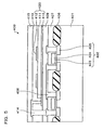
- FIG. 5 is a cross-sectional diagram showing an example of a ferroelectric memory device according to one embodiment of the invention in which a memory cell array and a peripheral circuit are integrated on a single substrate.
- FIGS. 6A and 6B are respectively a cross-sectional diagram and an equivalent circuit diagram schematically showing a 1T1C type ferroelectric memory according to a modification of one embodiment of the invention.
- FIG. 7 shows a sample formation method in an experimental example according to one embodiment of the invention.
- FIG. 8 shows crystallinity of a ferroelectric film sample in the experimental example.
- FIG. 9 shows hysteresis characteristics of a sample in the experimental example.
- the invention may provide a ferroelectric film which does not contain lead and exhibits high reliability, a method of manufacturing the same, a ferroelectric capacitor, and a ferroelectric memory.
- a ferroelectric film comprising BiNb0 4 .
- the BiNbO 4 may have a Bi-layered perovskite structure.
- This ferroelectric film may further comprise Si or Si and Ge.
- a method of manufacturing a ferroelectric film comprising:
- a method of manufacturing a ferroelectric film comprising:
- the organic solvent may be an alcohol.
- the step (a) may include mixing a sol-gel raw material containing Si or Si and Ge. It is preferable to add Si or Si and Ge to the precursor composition in an amount of 1 to 3 mol%.
- a ferroelectric raw material solution comprising:
- a ferroelectric raw material solution comprising:
- a ferroelectric capacitor comprising a ferroelectric film including BiNbO 4 .
- a ferroelectric memory comprising a ferroelectric film including BiNb0 4 .
- FIG. 1 is a cross-sectional diagram schematically showing a ferroelectric capacitor 100 using a ferroelectric film 101 according to one embodiment of the invention.
- the ferroelectric capacitor 100 includes a substrate 10, a first electrode 102, the ferroelectric film 101 formed on the first electrode 102, and a second electrode 103 formed on the ferroelectric film 101.
- the thicknesses of the first electrode 102 and the second electrode 103 are about 50 to 150 nm, for example.
- the ferroelectric film 101 includes BiNbO 4 and has a Bi-layered perovskite structure.
- the ferroelectric film 101 further includes Si or Si and Ge. The addition of Si or Si and Ge is described later.
- a Bi-layered perovskite has a crystal structure as shown in FIG 2.
- a plurality of octahedrons having oxygen at the vertices are disposed between layers formed by Bi.
- Nb is positioned inside the octahedron.
- the ferroelectric film 101 according to one embodiment of the invention includes a-phase (ferroelectric phase) BiNbO 4 .
- the thickness of the ferroelectric film 101 is about 50 to 150 nm, for example.
- a method of manufacturing a ferroelectric film and a ferroelectric capacitor according to one embodiment of the invention is described below.
- the substrate 10 is provided. As the material for the substrate 10, silicon or the like may be used.
- the first electrode 102 is formed on the substrate 10.
- the first electrode 102 may be formed by using a laser ablation method, for example. Specifically, a target containing a desired electrode material is provided. Then, atoms including an oxygen atom and a metal atom are scattered from the target by applying laser light to the target to cause a plume to occur. The plume is emitted toward the substrate 10 and caused to come in contact with the substrate 10. As a result, the first electrode 102 is epitaxially grown on the substrate 10.
- the material for the first electrode 102 is not particularly limited.
- Pt, Ir, IrO x , SrRuO 3 , Nb-SrTiO 3 , La-SrTiO 3 , Nb-(La,Sr)CoO 3 , LaNiO 3 , PbBaO 3 , or the like may be used.
- Nb-SrTiO 3 is obtained by doping SrTiO 3 with Nb
- La-SrTiO 3 is obtained by doping SrTiO 3 with La
- Nb-(La,Sr)CoO 3 is obtained by doping (La,Sr)CoO 3 with Nb.
- an ion beam assist method As the formation method for the first electrode 102, an ion beam assist method, a sputtering method, a vacuum deposition method, or the like may be used instead of the laser ablation method.
- the ferroelectric film 101 is formed on the first electrode 102.
- a polycarboxylate containing niobium, a polycarboxylate containing bismuth, a polycarboxylic acid or a polycarboxylic acid ester, and an organic solvent are mixed.
- niobium octylate As the polycarboxylate containing niobium, niobium octylate or the like may be used. As shown in the FIG. 3, niobium octylate has a structure in which two Nb atoms form a covalent bond and an octyl group exists in the remaining site.
- the network formation between the polycarboxylic acid and niobium octylate proceeds mainly by an alcohol exchange reaction. Specifically, a reaction occurs between the carboxylic acid and the octyl group (alcohol exchange reaction) so that esterification (R-COO-Nb) proceeds.
- the molecule of niobium octylate can be bonded to the precursor network by condensation between niobium octylate and an alkoxide by esterifying niobium octylate.
- bismuth octylate As the polycarboxylate containing bismuth, bismuth octylate or the like may be used.
- the network formation of bismuth octylate proceeds mainly by an alcohol exchange reaction in the same manner as niobium octylate.
- an alcohol may be used as the organic solvent used in one embodiment of the invention.
- a sol-gel raw material and the polycarboxylic acid or the polycarboxylic acid ester can be efficiently dissolved by using an alcohol as the solvent.
- the alcohol is not particularly limited.
- monohydric alcohols such as butanol, methanol, ethanol, and propanol
- polyhydric alcohols can be given. Specific examples of such an alcohol are given below.
- the polycarboxylic acid or the polycarboxylic acid ester be a dicarboxylic acid or a dicarboxylic acid ester.
- polycarboxylic acid examples include the following compounds.
- a tricarboxylic acid trans-aconitic acid, trimesic acid, and the like can be given.
- a tetracarboxylic acid examples of pyromellitic acid, 1,2,3,4-cyclopentanetetracarboxylic acid, and the like are can be given.
- dicarboxylic acid esters such as dimethyl succinate, diethyl succinate, dibutyl oxalate, dimethyl malonate, dimethyl adipate, dimethyl maleate, and diethyl fumarate
- tricarboxylic acid esters such as tributyl citrate and triethyl 1,1,2-ethanetricarboxylate
- tetracarboxylic acid esters such as tetraethyl 1,1,2,2-ethanetetracarboxylate and trimethyl 1,2,4-benzenetricarboxylate, and the like can be given.
- polycarboxylic acid esters dissociate in the presence of an alcohol and function as polycarboxylic acids.
- a feature of one embodiment of the invention is that the network is grown by esterification using the polycarboxylic acid. Since the ester network is not grown when using a monocarboxylic acid or a monocarboxylic acid ester, such as acetic acid or methyl acetate, a monocarboxylic acid or a monocarboxylic acid ester is not used in one embodiment of the invention.
- the dicarboxylic acid ester may be preferably at least one ester selected from a succinic acid ester, a maleic acid ester, and a malonic acid ester.
- a succinic acid ester a maleic acid ester
- a malonic acid ester a malonic acid ester.
- dimethyl succinate, dimethyl maleate, and dimethyl malonate can be given.
- a sol-gel raw material containing Si or Si and Ge may be used as a sol-gel raw material including a hydrolysis-condensation product of a metal alkoxide.
- a sol-gel solution a PbSiO 3 sol-gel solution or a combination of a PbSiO 3 sol-gel solution and a PbGeO 3 sol-gel solution may be used.
- the deposition temperature can be reduced by using a sol-gel raw material containing Si or Ge, so that a ferroelectric can be crystallized at about 450°C.
- Alpha (a)-phase (ferroelectric phase) BiNbO 4 can be more reliably obtained by adding Si or Si and Ge.
- the ferroelectric film 101 may be formed by applying the mixed solution to the substrate and crystallizing the applied solution by heat treatment or the like.
- a series of steps consisting of a mixed solution coating step, an alcohol removal step, a drying heat treatment step, and a cleaning heat treatment step is performed a desired number of times, and the resulting product is sintered by crystallization annealing to form the ferroelectric film 101.
- the conditions in each step are as follows.
- the mixed solution coating step is performed by applying the mixed solution by using a coating method such as spin coating.
- a coating method such as spin coating.
- a spin operation is performed in order to spread the applied solution over the entire surface of the substrate.
- the rotational speed of the spin operation is set at about 500 rpm, for example.
- the spin operation is performed at a lower rotational speed for a desired period of time so that the first electrode 102 is coated with the mixed solution.
- the rotational speed of this spin operation is set at 50 rpm or less, for example.
- the drying heat treatment step is performed at 150 to 180°C.
- the drying heat treatment is performed in air by using a hot plate or the like.
- the cleaning heat treatment step is performed in air on a hot plate maintained at 300 to 350°C.
- the crystallization sintering step is performed in an oxygen atmosphere by rapid thermal annealing (RTA) or the like.
- the thickness of the ferroelectric film 101 after sintering may be about 50 to 150 nm.
- the ferroelectric film 101 may be formed by using a sputtering method, a molecular beam epitaxy method, a laser ablation method, or the like.
- a sol-gel raw material including a hydrolysis-condensation product of a metal alkoxide containing niobium and a sol-gel raw material including a hydrolysis-condensation product of a metal alkoxide containing bismuth may be used instead of the polycarboxylate containing niobium and the polycarboxylate containing bismuth.
- a ferroelectric precursor composition may be prepared by mixing the sol-gel raw material including a hydrolysis-condensation product of a metal alkoxide containing niobium, the sol-gel raw material including a hydrolysis-condensation product of a metal alkoxide containing bismuth, the polycarboxylic acid or the polycarboxylic acid ester, and the organic solvent, and causing the polycarboxylic acid or a polycarboxylic acid derived from polycarboxylic acid ester to undergo esterification with the metal alkoxide containing niobium and the metal alkoxide containing bismuth.
- the formation reaction of the precursor composition is roughly divided into a first-stage alkoxy group substitution reaction and a second-stage polymer network formation reaction by esterification.
- dimethyl succinate and the metal alkoxide of the sol-gel raw material are esterified to form an ester bond.
- dimethyl succinate dissociates in n-butanol so that one of the carbonyl groups (first carbonyl group) is protonated.
- a substitution reaction occurs between the first carbonyl group and the alkoxy group of the metal alkoxide so that a reaction product, in which the first carboxyl group is esterified, and an alcohol are produced.
- the "ester bond” used herein means a bond (-COO-) formed by a carbonyl group and an oxygen atom.
- a substitution reaction occurs between the other carboxyl group (second carboxyl group), which remained unreacted in the first-stage reaction, and the alkoxy group of the metal alkoxide so that a reaction product, in which the second carboxyl group is esterified, and an alcohol are produced.
- a polymer network in which the hydrolysis-condensation products of the metal alkoxide contained in the sol-gel raw material are bonded through ester bonds is obtained by the above two-stage reaction. Therefore, this polymer network contains a moderate amount of ester bond in the network.
- the second electrode 103 is formed on the ferroelectric film 101.
- the second electrode 103 may be formed by using a sputtering method, a vacuum deposition method, or the like. It is preferable to use a material mainly containing Pt for the upper electrode.
- the material for the second electrode 103 is not limited to Pt.
- a known electrode material such as Ir, IrO x , SrRuO 3 , Nb-SrTiO 3 , La-SrTiO 3 , Nb-(La,Sr)CoO 3 , LaNiO 3 , or PbBaO 3 may also be used.
- post annealing may optionally be performed in an oxygen atmosphere by RTA or the like. This enables an excellent interface to be formed between the second electrode 103 and the ferroelectric film 101 and improves the crystallinity of the ferroelectric film 101.
- the ferroelectric film 101 and the ferroelectric capacitor 100 according to one embodiment of the invention can be manufactured by the above-described steps.
- the crystallization temperature can be reduced and the hysteresis squareness can be improved.
- An improvement of the hysteresis squareness by the ferroelectric capacitor 100 has an effect on stability against a disturbance, which is important for driving a simple matrix type ferroelectric memory device.
- FIGS. 4A and 4B are diagrams showing a configuration of a simple matrix type ferroelectric memory device 300 according to one embodiment of the invention.
- FIG. 4A is a plan view of the ferroelectric memory device 300
- FIG. 4B is a cross-sectional diagram along the line A-A shown in FIG 4A.
- the ferroelectric memory device 300 includes a specific number of wordlines 301 to 303 formed on a substrate 308, and a specific number of bitlines 304 to 306.
- a ferroelectric film 307 described in the above-described embodiment is inserted between the wordlines 301 to 303 and the bitlines 304 to 306, so that ferroelectric capacitors are formed at the intersecting regions of the wordlines 301 to 303 and the bitlines 304 to 306.
- peripheral circuit In the ferroelectric memory device 300 in which memory cells are arranged in a simple matrix, data is written into or read from the ferroelectric capacitors formed in the intersecting regions of the wordlines 301 to 303 and the bitlines 304 to 306 by using a peripheral driver circuit, a read amplifier circuit, and the like (not shown) (hereinafter collectively called "peripheral circuit").
- the peripheral circuit may be formed by forming MOS transistors on a substrate differing from the substrate of the memory cell array and connecting the MOS transistors with the wordlines 301 to 303 and the bitlines 304 to 306.
- the peripheral circuit and the memory cell array may be integrated on a single substrate by using a single-crystal silicon substrate as the substrate 308.
- FIG. 5 is a cross-sectional diagram showing an example of a ferroelectric memory device 400 according to one embodiment of the invention in which a memory cell array and a peripheral circuit are integrated on a single substrate.
- MOS transistors 402 are formed on a single-crystal silicon substrate 401, and the transistor formation region corresponds to a peripheral circuit section.
- the MOS transistor 402 is formed by the single-crystal silicon substrate 401, source/drain regions 405, a gate insulating film 403, and a gate electrode 404.
- the ferroelectric memory device 400 includes an element isolation oxide film 406, a first interlayer dielectric 407, a first interconnect layer 408, and a second interlayer dielectric 409.
- the ferroelectric memory device 400 includes a memory cell array including ferroelectric capacitors 420.
- the ferroelectric capacitor 420 includes a lower electrode 410 (first electrode or second electrode) functioning as a wordline or a bitline, a ferroelectric film 411 including a ferroelectric phase and a paraelectric phase, and an upper electrode 412 (second electrode or first electrode) formed on the ferroelectric film 411 and functioning as the bitline or the wordline.
- the ferroelectric memory device 400 includes a third interlayer dielectric 413 over the ferroelectric capacitor 420.
- the memory cell array is connected with the peripheral circuit section through a second interconnection layer 414.
- a protective film 415 is formed over the third interlayer dielectric 413 and the second interconnect layer 414.
- the memory cell array and the peripheral circuit section can be integrated on a single substrate.
- the ferroelectric memory device 400 shown in FIG 5 has a configuration in which the memory cell array is formed over the peripheral circuit section.
- the ferroelectric memory device 400 may have a configuration in which the memory cell array is not disposed over the peripheral circuit section and is adjacent to the peripheral circuit section in the horizontal direction.
- the ferroelectric capacitor 420 used in one embodiment of the invention includes the ferroelectric film according to the above-described embodiment, the ferroelectric capacitor 420 exhibits excellent hysteresis squareness and has stable disturbance characteristics. Moreover, since the ferroelectric capacitor 420 allows a decrease in process temperature, damage to the peripheral circuit and other elements is reduced. Furthermore, since process damage (particularly reduction by hydrogen) occurs to only a small extent, hysteresis deterioration due to damage can be prevented. Therefore, the simple matrix type ferroelectric memory device 300 can be put into practical use by using the ferroelectric capacitor 420.
- FIG. 6A is a structural diagram of a 1T1C type ferroelectric memory device 500 as a modification.
- FIG. 6B is an equivalent circuit diagram of the ferroelectric memory device 500.
- the ferroelectric memory device 500 is a memory device having a structure similar to that of a DRAM, and includes a capacitor 504 (1C) including a lower electrode 501, an upper electrode 502 connected with a plate line, and a ferroelectric film 503 according to the above-described embodiment, and a switch transistor element 507 (IT) including source/drain electrodes, one of which is connected with a data line 505, and a gate electrode 506 connected with a wordline. Since the 1T1C type memory allows high-speed writing and reading (100 ns or less) and written data does not volatilize, the 1T1C type memory is expected to replace an SRAM.
- a ferroelectric film according to one embodiment of the invention was formed by using a raw material solution described below.
- Dimethyl succinate was mixed in an amount of 0.5 mol/l for 1 mol/l of the metal element concentration of the raw material solution.
- the raw material solution was then sealed and allowed to stand at 90°C for 30 min.
- the raw material solution was then cooled to room temperature to cause esterification to sufficiently proceed.
- a sample was prepared by using the resulting solution according a method shown in FIG. 7.
- a platinum lower electrode was formed by using a sputtering method.
- the raw material solution was applied to the platinum substrate by using a spin coating method, and dried at 150 to 180°C (150°C) by using a hot plate to remove the alcohol.
- a cleaning heat treatment was performed at 300 to 350°C (300°C) by using a hot plate.
- the coating step, the drying treatment step, and the cleaning heat treatment step were arbitrarily performed a number of times (three times in total) to obtain a coating film having a desired thickness.
- the coating film was then subjected to crystallization annealing (sintering) to obtain a ferroelectric film sample having a thickness of 150 nm.
- the crystallization sintering was performed in an oxygen atmosphere at 650 to 700°C (650°C) by rapid thermal annealing (RTA). Then, a platinum upper electrode was formed by using a sputtering method, and recovery annealing was performed at 650 to 700°C (650°C) by RTA to obtain a ferroelectric capacitor sample (hereinafter may be called "capacitor sample").
- RTA rapid thermal annealing
- FIG. 8 is a diagram showing the crystallinity of the ferroelectric film sample. As shown in FIG 8, (141) and (211) peaks attributed to BiNbO 4 were recognized so that it was confirmed that a crystal having a bismuth-layered perovskite structure was formed.
- FIG. 9 is a hysteresis diagram of the capacitor sample. As shown in FIG 9, it was confirmed that each capacitor sample had excellent hysteresis characteristics.
Abstract
Description
- The present invention relates to a ferroelectric film and a method of manufacturing the same.
- A ferroelectric such as PZT has been used for various applications such as a ferroelectric memory, a piezoelectric device, and an infrared sensor, and has been extensively researched and developed.
- In particular, the ferroelectric memory is nonvolatile and is expected to serve as a next-generation memory having an operation speed equal to the operation speed of a DRAM. Moreover, the ferroelectric memory consumes a small amount of power in comparison with other memories.
- However, since a ferroelectric material such as PZT contains a large amount of lead which is harmful to the human body, it is not desirable to mass-produce such a ferroelectric material. Moreover, since lead contained in PZT easily volatilizes, oxygen deficiency tends to occur due to low bonding energy with lead.
- According to a first aspect of the invention, there is provided a ferroelectric film, comprising BiNbO4.
- According to a second aspect of the invention, there is provided a method of manufacturing a ferroelectric film, the method comprising:
- (a) mixing a polycarboxylate containing niobium, a polycarboxylate containing bismuth, a polycarboxylic acid or a polycarboxylic acid ester, and an organic solvent; and
- (b) applying the resulting mixed solution to a substrate and heat-treating the applied mixed solution to form a ferroelectric film including BiNbO4.
- According to a third aspect of the invention, there is provided a method of manufacturing a ferroelectric film, the method comprising:
- (a) mixing a sol-gel raw material including a hydrolysis-condensation product of a metal alkoxide containing niobium, a sol-gel raw material including a hydrolysis-condensation product of a metal alkoxide containing bismuth, a polycarboxylic acid or a polycarboxylic acid ester, and an organic solvent, and causing the polycarboxylic acid or a polycarboxylic acid derived from the polycarboxylic acid ester to undergo esterification with the metal alkoxide containing niobium and the metal alkoxide containing bismuth to prepare a ferroelectric precursor composition; and
- (b) applying the precursor composition to a substrate and heat-treating the applied precursor composition to form a ferroelectric film including BiNbO4.
- According to a fourth aspect of the invention, there is provided a ferroelectric raw material solution, comprising:
- a polycarboxylate containing niobium;
- a polycarboxylate containing bismuth;
- a polycarboxylic acid or a polycarboxylic acid ester; and
- an organic solvent.
- According to a fifth aspect of the invention, there is provided a ferroelectric raw material solution, comprising:
- a sol-gel raw material including a hydrolysis-condensation product of a metal alkoxide containing niobium;
- a sol-gel raw material including a hydrolysis-condensation product of a metal alkoxide containing bismuth;
- a polycarboxylic acid or a polycarboxylic acid ester; and
- an organic solvent.
- According to a sixth aspect of the invention, there is provided a ferroelectric capacitor, comprising a ferroelectric film including BiNbO4.
- According to a seventh aspect of the invention, there is provided a ferroelectric memory, comprising a ferroelectric film including BiNb04.
- FIG. 1 is a cross-sectional diagram showing a ferroelectric capacitor according to one embodiment of the invention.
- FIG. 2 is a diagram illustrative of a Bi-layered perovskite type crystal structure.
- FIG. 3 is a diagram showing niobium octylate used in one embodiment of the invention.
- FIGS. 4A and 4B are respectively a plan view and a cross-sectional diagram schematically showing a simple matrix type ferroelectric memory device according to one embodiment of the invention.
- FIG. 5 is a cross-sectional diagram showing an example of a ferroelectric memory device according to one embodiment of the invention in which a memory cell array and a peripheral circuit are integrated on a single substrate.
- FIGS. 6A and 6B are respectively a cross-sectional diagram and an equivalent circuit diagram schematically showing a 1T1C type ferroelectric memory according to a modification of one embodiment of the invention.
- FIG. 7 shows a sample formation method in an experimental example according to one embodiment of the invention.
- FIG. 8 shows crystallinity of a ferroelectric film sample in the experimental example.
- FIG. 9 shows hysteresis characteristics of a sample in the experimental example.
- The invention may provide a ferroelectric film which does not contain lead and exhibits high reliability, a method of manufacturing the same, a ferroelectric capacitor, and a ferroelectric memory.
- According to one embodiment of the invention, there is provided a ferroelectric film, comprising BiNb04.
- In this ferroelectric film, the BiNbO4 may have a Bi-layered perovskite structure.
- This ferroelectric film may further comprise Si or Si and Ge.
- According to one embodiment of the invention, there is provided a method of manufacturing a ferroelectric film, the method comprising:
- (a) mixing a polycarboxylate containing niobium, a polycarboxylate containing bismuth, a polycarboxylic acid or a polycarboxylic acid ester, and an organic solvent; and
- (b) applying the resulting mixed solution to a substrate and heat-treating the applied mixed solution to form a ferroelectric film including BiNbO4.
- According to one embodiment of the invention, there is provided a method of manufacturing a ferroelectric film, the method comprising:
- (a) mixing a sol-gel raw material including a hydrolysis-condensation product of a metal alkoxide containing niobium, a sol-gel raw material including a hydrolysis-condensation product of a metal alkoxide containing bismuth, a polycarboxylic acid or a polycarboxylic acid ester, and an organic solvent, and causing the polycarboxylic acid or a polycarboxylic acid derived from the polycarboxylic acid ester to undergo esterification with the metal alkoxide containing niobium and the metal alkoxide containing bismuth to prepare a ferroelectric precursor composition; and
- (b) applying the precursor composition to a substrate and heat-treating the applied precursor composition to form a ferroelectric film including BiNb04.
- In the above methods of manufacturing a ferroelectric film, the organic solvent may be an alcohol.
- In the above methods of manufacturing a ferroelectric film, the step (a) may include mixing a sol-gel raw material containing Si or Si and Ge. It is preferable to add Si or Si and Ge to the precursor composition in an amount of 1 to 3 mol%.
- According to one embodiment of the invention, there is provided a ferroelectric raw material solution, comprising:
- a polycarboxylate containing niobium;
- a polycarboxylate containing bismuth;
- a polycarboxylic acid or a polycarboxylic acid ester; and
- an organic solvent.
- According to one embodiment of the invention, there is provided a ferroelectric raw material solution, comprising:
- a sol-gel raw material including a hydrolysis-condensation product of a metal alkoxide containing niobium;
- a sol-gel raw material including a hydrolysis-condensation product of a metal alkoxide containing bismuth;
- a polycarboxylic acid or a polycarboxylic acid ester; and
- an organic solvent.
- According to one embodiment of the invention, there is provided a ferroelectric capacitor, comprising a ferroelectric film including BiNbO4.
- According to one embodiment of the invention, there is provided a ferroelectric memory, comprising a ferroelectric film including BiNb04.
- These embodiments of the invention will be described in detail below, with reference to the drawings.
- FIG. 1 is a cross-sectional diagram schematically showing a
ferroelectric capacitor 100 using aferroelectric film 101 according to one embodiment of the invention. - As shown in FIG. 1, the
ferroelectric capacitor 100 includes asubstrate 10, afirst electrode 102, theferroelectric film 101 formed on thefirst electrode 102, and asecond electrode 103 formed on theferroelectric film 101. - The thicknesses of the
first electrode 102 and thesecond electrode 103 are about 50 to 150 nm, for example. - The
ferroelectric film 101 includes BiNbO4 and has a Bi-layered perovskite structure. Theferroelectric film 101 further includes Si or Si and Ge. The addition of Si or Si and Ge is described later. - A Bi-layered perovskite has a crystal structure as shown in FIG 2. A plurality of octahedrons having oxygen at the vertices are disposed between layers formed by Bi. Nb is positioned inside the octahedron. The
ferroelectric film 101 according to one embodiment of the invention includes a-phase (ferroelectric phase) BiNbO4. The thickness of theferroelectric film 101 is about 50 to 150 nm, for example. - A method of manufacturing a ferroelectric film and a ferroelectric capacitor according to one embodiment of the invention is described below.
- The
substrate 10 is provided. As the material for thesubstrate 10, silicon or the like may be used. - The
first electrode 102 is formed on thesubstrate 10. Thefirst electrode 102 may be formed by using a laser ablation method, for example. Specifically, a target containing a desired electrode material is provided. Then, atoms including an oxygen atom and a metal atom are scattered from the target by applying laser light to the target to cause a plume to occur. The plume is emitted toward thesubstrate 10 and caused to come in contact with thesubstrate 10. As a result, thefirst electrode 102 is epitaxially grown on thesubstrate 10. - The material for the
first electrode 102 is not particularly limited. For example, Pt, Ir, IrOx, SrRuO3, Nb-SrTiO3, La-SrTiO3, Nb-(La,Sr)CoO3, LaNiO3, PbBaO3, or the like may be used. Nb-SrTiO3 is obtained by doping SrTiO3 with Nb, La-SrTiO3 is obtained by doping SrTiO3 with La, and Nb-(La,Sr)CoO3 is obtained by doping (La,Sr)CoO3 with Nb. - As the formation method for the
first electrode 102, an ion beam assist method, a sputtering method, a vacuum deposition method, or the like may be used instead of the laser ablation method. - Then, the
ferroelectric film 101 is formed on thefirst electrode 102. - A polycarboxylate containing niobium, a polycarboxylate containing bismuth, a polycarboxylic acid or a polycarboxylic acid ester, and an organic solvent are mixed.
- As the polycarboxylate containing niobium, niobium octylate or the like may be used. As shown in the FIG. 3, niobium octylate has a structure in which two Nb atoms form a covalent bond and an octyl group exists in the remaining site.
- The network formation between the polycarboxylic acid and niobium octylate proceeds mainly by an alcohol exchange reaction. Specifically, a reaction occurs between the carboxylic acid and the octyl group (alcohol exchange reaction) so that esterification (R-COO-Nb) proceeds. According to one embodiment of the invention, the molecule of niobium octylate can be bonded to the precursor network by condensation between niobium octylate and an alkoxide by esterifying niobium octylate.
- As the polycarboxylate containing bismuth, bismuth octylate or the like may be used. The network formation of bismuth octylate proceeds mainly by an alcohol exchange reaction in the same manner as niobium octylate.
- As the organic solvent used in one embodiment of the invention, an alcohol may be used. A sol-gel raw material and the polycarboxylic acid or the polycarboxylic acid ester can be efficiently dissolved by using an alcohol as the solvent.
- The alcohol is not particularly limited. As examples of the alcohol, monohydric alcohols such as butanol, methanol, ethanol, and propanol, and polyhydric alcohols can be given. Specific examples of such an alcohol are given below.
-
- Propanol (propyl alcohol): 1-propanol (boiling point: 97.4°C) and 2-propanol (boiling point:82.7°C)
- Butanol (butyl alcohol): 1-butanol (boiling point: 117°C), 2-butanol (boiling point: 100°C), 2-methyl-1-propanol (boiling point: 108°C), and 2-methyl-2-propanol (melting point: 25.4°C, boiling point: 83°C)
- Pentanol (amyl alcohol): 1-pentanol (boiling point: 137°C), 3-methyl-l-butanol (boiling point: 131°C), 2-methyl-l-butanol (boiling point: 128°C), 2,2-dimethyl-l-propanol (boiling point: 113°C), 2-pentanol (boiling point: 119°C), 3-methyl-2-butanol (boiling point: 112.5°C), 3-pentanol (boiling point: 117°C), and 2-methyl-2-butanol (boiling point: 102°C)
-
- Ethylene glycol (melting point: -11.5°C, boiling point: 197.5°C) and glycerol (melting point: 17°C, boiling point: 290°C)
- It is preferable that the polycarboxylic acid or the polycarboxylic acid ester be a dicarboxylic acid or a dicarboxylic acid ester.
- As examples of the polycarboxylic acid, the following compounds can be given. As examples of a tricarboxylic acid, trans-aconitic acid, trimesic acid, and the like can be given. As examples of a tetracarboxylic acid, pyromellitic acid, 1,2,3,4-cyclopentanetetracarboxylic acid, and the like are can be given. As examples of a polycarboxylic acid ester which dissociates in an alcohol and functions as a polycarboxylic acid, dicarboxylic acid esters such as dimethyl succinate, diethyl succinate, dibutyl oxalate, dimethyl malonate, dimethyl adipate, dimethyl maleate, and diethyl fumarate, tricarboxylic acid esters such as tributyl citrate and
triethyl tetraethyl trimethyl - The dicarboxylic acid ester may be preferably at least one ester selected from a succinic acid ester, a maleic acid ester, and a malonic acid ester. As specific examples of these esters, dimethyl succinate, dimethyl maleate, and dimethyl malonate can be given.
- In the method of manufacturing a ferroelectric film according to one embodiment of the invention, a sol-gel raw material containing Si or Si and Ge may be used as a sol-gel raw material including a hydrolysis-condensation product of a metal alkoxide. As such a sol-gel solution, a PbSiO3 sol-gel solution or a combination of a PbSiO3 sol-gel solution and a PbGeO3 sol-gel solution may be used. The deposition temperature can be reduced by using a sol-gel raw material containing Si or Ge, so that a ferroelectric can be crystallized at about 450°C.
- Alpha (a)-phase (ferroelectric phase) BiNbO4 can be more reliably obtained by adding Si or Si and Ge.
- The
ferroelectric film 101 may be formed by applying the mixed solution to the substrate and crystallizing the applied solution by heat treatment or the like. - In more detail, a series of steps consisting of a mixed solution coating step, an alcohol removal step, a drying heat treatment step, and a cleaning heat treatment step is performed a desired number of times, and the resulting product is sintered by crystallization annealing to form the
ferroelectric film 101. The conditions in each step are as follows. - The mixed solution coating step is performed by applying the mixed solution by using a coating method such as spin coating. First, the mixed solution is applied dropwise to the
first electrode 102. A spin operation is performed in order to spread the applied solution over the entire surface of the substrate. The rotational speed of the spin operation is set at about 500 rpm, for example. Then, the spin operation is performed at a lower rotational speed for a desired period of time so that thefirst electrode 102 is coated with the mixed solution. The rotational speed of this spin operation is set at 50 rpm or less, for example. The drying heat treatment step is performed at 150 to 180°C. The drying heat treatment is performed in air by using a hot plate or the like. The cleaning heat treatment step is performed in air on a hot plate maintained at 300 to 350°C. The crystallization sintering step is performed in an oxygen atmosphere by rapid thermal annealing (RTA) or the like. - The thickness of the
ferroelectric film 101 after sintering may be about 50 to 150 nm. Theferroelectric film 101 may be formed by using a sputtering method, a molecular beam epitaxy method, a laser ablation method, or the like. - A sol-gel raw material including a hydrolysis-condensation product of a metal alkoxide containing niobium and a sol-gel raw material including a hydrolysis-condensation product of a metal alkoxide containing bismuth may be used instead of the polycarboxylate containing niobium and the polycarboxylate containing bismuth. A ferroelectric precursor composition may be prepared by mixing the sol-gel raw material including a hydrolysis-condensation product of a metal alkoxide containing niobium, the sol-gel raw material including a hydrolysis-condensation product of a metal alkoxide containing bismuth, the polycarboxylic acid or the polycarboxylic acid ester, and the organic solvent, and causing the polycarboxylic acid or a polycarboxylic acid derived from polycarboxylic acid ester to undergo esterification with the metal alkoxide containing niobium and the metal alkoxide containing bismuth.
- The formation reaction of the precursor composition is roughly divided into a first-stage alkoxy group substitution reaction and a second-stage polymer network formation reaction by esterification.
- In the first-stage reaction, dimethyl succinate and the metal alkoxide of the sol-gel raw material are esterified to form an ester bond. Specifically, dimethyl succinate dissociates in n-butanol so that one of the carbonyl groups (first carbonyl group) is protonated. A substitution reaction occurs between the first carbonyl group and the alkoxy group of the metal alkoxide so that a reaction product, in which the first carboxyl group is esterified, and an alcohol are produced. The "ester bond" used herein means a bond (-COO-) formed by a carbonyl group and an oxygen atom.
- In the second-stage reaction, a substitution reaction occurs between the other carboxyl group (second carboxyl group), which remained unreacted in the first-stage reaction, and the alkoxy group of the metal alkoxide so that a reaction product, in which the second carboxyl group is esterified, and an alcohol are produced.
- A polymer network in which the hydrolysis-condensation products of the metal alkoxide contained in the sol-gel raw material are bonded through ester bonds is obtained by the above two-stage reaction. Therefore, this polymer network contains a moderate amount of ester bond in the network.
- Then, the
second electrode 103 is formed on theferroelectric film 101. Thesecond electrode 103 may be formed by using a sputtering method, a vacuum deposition method, or the like. It is preferable to use a material mainly containing Pt for the upper electrode. The material for thesecond electrode 103 is not limited to Pt. A known electrode material such as Ir, IrOx, SrRuO3, Nb-SrTiO3, La-SrTiO3, Nb-(La,Sr)CoO3, LaNiO3, or PbBaO3 may also be used. - Then, post annealing may optionally be performed in an oxygen atmosphere by RTA or the like. This enables an excellent interface to be formed between the
second electrode 103 and theferroelectric film 101 and improves the crystallinity of theferroelectric film 101. - The
ferroelectric film 101 and theferroelectric capacitor 100 according to one embodiment of the invention can be manufactured by the above-described steps. - According to the
ferroelectric capacitor 100 of one embodiment of the invention, the crystallization temperature can be reduced and the hysteresis squareness can be improved. An improvement of the hysteresis squareness by theferroelectric capacitor 100 has an effect on stability against a disturbance, which is important for driving a simple matrix type ferroelectric memory device. - FIGS. 4A and 4B are diagrams showing a configuration of a simple matrix type
ferroelectric memory device 300 according to one embodiment of the invention. FIG. 4A is a plan view of theferroelectric memory device 300, and FIG. 4B is a cross-sectional diagram along the line A-A shown in FIG 4A. As shown in FIGS. 4A and 4B, theferroelectric memory device 300 includes a specific number ofwordlines 301 to 303 formed on asubstrate 308, and a specific number ofbitlines 304 to 306. Aferroelectric film 307 described in the above-described embodiment is inserted between thewordlines 301 to 303 and thebitlines 304 to 306, so that ferroelectric capacitors are formed at the intersecting regions of thewordlines 301 to 303 and thebitlines 304 to 306. - In the
ferroelectric memory device 300 in which memory cells are arranged in a simple matrix, data is written into or read from the ferroelectric capacitors formed in the intersecting regions of thewordlines 301 to 303 and thebitlines 304 to 306 by using a peripheral driver circuit, a read amplifier circuit, and the like (not shown) (hereinafter collectively called "peripheral circuit"). The peripheral circuit may be formed by forming MOS transistors on a substrate differing from the substrate of the memory cell array and connecting the MOS transistors with thewordlines 301 to 303 and thebitlines 304 to 306. Or, the peripheral circuit and the memory cell array may be integrated on a single substrate by using a single-crystal silicon substrate as thesubstrate 308. - FIG. 5 is a cross-sectional diagram showing an example of a
ferroelectric memory device 400 according to one embodiment of the invention in which a memory cell array and a peripheral circuit are integrated on a single substrate. - In FIG. 5,
MOS transistors 402 are formed on a single-crystal silicon substrate 401, and the transistor formation region corresponds to a peripheral circuit section. TheMOS transistor 402 is formed by the single-crystal silicon substrate 401, source/drain regions 405, agate insulating film 403, and agate electrode 404. Theferroelectric memory device 400 includes an elementisolation oxide film 406, afirst interlayer dielectric 407, afirst interconnect layer 408, and asecond interlayer dielectric 409. - The
ferroelectric memory device 400 includes a memory cell array includingferroelectric capacitors 420. Theferroelectric capacitor 420 includes a lower electrode 410 (first electrode or second electrode) functioning as a wordline or a bitline, aferroelectric film 411 including a ferroelectric phase and a paraelectric phase, and an upper electrode 412 (second electrode or first electrode) formed on theferroelectric film 411 and functioning as the bitline or the wordline. - The
ferroelectric memory device 400 includes athird interlayer dielectric 413 over theferroelectric capacitor 420. The memory cell array is connected with the peripheral circuit section through asecond interconnection layer 414. In theferroelectric memory device 400, aprotective film 415 is formed over thethird interlayer dielectric 413 and thesecond interconnect layer 414. - According to the
ferroelectric memory device 400 having the above-described configuration, the memory cell array and the peripheral circuit section can be integrated on a single substrate. Theferroelectric memory device 400 shown in FIG 5 has a configuration in which the memory cell array is formed over the peripheral circuit section. However, theferroelectric memory device 400 may have a configuration in which the memory cell array is not disposed over the peripheral circuit section and is adjacent to the peripheral circuit section in the horizontal direction. - Since the
ferroelectric capacitor 420 used in one embodiment of the invention includes the ferroelectric film according to the above-described embodiment, theferroelectric capacitor 420 exhibits excellent hysteresis squareness and has stable disturbance characteristics. Moreover, since theferroelectric capacitor 420 allows a decrease in process temperature, damage to the peripheral circuit and other elements is reduced. Furthermore, since process damage (particularly reduction by hydrogen) occurs to only a small extent, hysteresis deterioration due to damage can be prevented. Therefore, the simple matrix typeferroelectric memory device 300 can be put into practical use by using theferroelectric capacitor 420. - FIG. 6A is a structural diagram of a 1T1C type
ferroelectric memory device 500 as a modification. FIG. 6B is an equivalent circuit diagram of theferroelectric memory device 500. - As shown in FIG 6A, the
ferroelectric memory device 500 is a memory device having a structure similar to that of a DRAM, and includes a capacitor 504 (1C) including alower electrode 501, anupper electrode 502 connected with a plate line, and aferroelectric film 503 according to the above-described embodiment, and a switch transistor element 507 (IT) including source/drain electrodes, one of which is connected with adata line 505, and agate electrode 506 connected with a wordline. Since the 1T1C type memory allows high-speed writing and reading (100 ns or less) and written data does not volatilize, the 1T1C type memory is expected to replace an SRAM. - Examples of the embodiments of the invention are described above. However, the invention is not limited to the above-described embodiments. Various modifications and variations may be made within the scope of the invention.
- An experimental example of the invention is described below.
- A ferroelectric film according to one embodiment of the invention was formed by using a raw material solution described below.
- A solution was prepared by mixing bismuth octylate and niobium octylate in a solvent such as n-butanol at a molar ratio of "bismuth octylate:niobium octylate = 1:1" together with 1.5 mol% of Si.
- The above solution and dimethyl succinate were mixed to prepare a raw material solution. Dimethyl succinate was mixed in an amount of 0.5 mol/l for 1 mol/l of the metal element concentration of the raw material solution. The raw material solution was then sealed and allowed to stand at 90°C for 30 min. The raw material solution was then cooled to room temperature to cause esterification to sufficiently proceed.
- A sample was prepared by using the resulting solution according a method shown in FIG. 7.
- Specifically, a platinum lower electrode was formed by using a sputtering method. The raw material solution was applied to the platinum substrate by using a spin coating method, and dried at 150 to 180°C (150°C) by using a hot plate to remove the alcohol. A cleaning heat treatment was performed at 300 to 350°C (300°C) by using a hot plate. The coating step, the drying treatment step, and the cleaning heat treatment step were arbitrarily performed a number of times (three times in total) to obtain a coating film having a desired thickness. The coating film was then subjected to crystallization annealing (sintering) to obtain a ferroelectric film sample having a thickness of 150 nm. The crystallization sintering was performed in an oxygen atmosphere at 650 to 700°C (650°C) by rapid thermal annealing (RTA). Then, a platinum upper electrode was formed by using a sputtering method, and recovery annealing was performed at 650 to 700°C (650°C) by RTA to obtain a ferroelectric capacitor sample (hereinafter may be called "capacitor sample").
- The following characteristics were examined by using the resulting sample.
- The crystallinity of the ferroelectric film sample was examined by X-ray diffraction analysis. FIG. 8 is a diagram showing the crystallinity of the ferroelectric film sample. As shown in FIG 8, (141) and (211) peaks attributed to BiNbO4 were recognized so that it was confirmed that a crystal having a bismuth-layered perovskite structure was formed.
- FIG. 9 is a hysteresis diagram of the capacitor sample. As shown in FIG 9, it was confirmed that each capacitor sample had excellent hysteresis characteristics.
- Although only some embodiments of the invention have been described in detail above, those skilled in the art will readily appreciate that many modifications are possible in the embodiments without departing from the novel teachings and advantages of this invention. Accordingly, all such modifications are intended to be included within the scope of this invention.
Claims (11)
- A ferroelectric film, comprising BiNbO4.
- The ferroelectric film as defined in claim 1,
wherein the BiNbO4 has a Bi-layered perovskite structure. - The ferroelectric film as defined in claim 1 or 2, further comprising Si or Si and Ge.
- A method of manufacturing a ferroelectric film, the method comprising:(a) mixing a polycarboxylate containing niobium, a polycarboxylate containing bismuth, a polycarboxylic acid or a polycarboxylic acid ester, and an organic solvent; and(b) applying the resulting mixed solution to a substrate and heat-treating the applied mixed solution to form a ferroelectric film including BiNbO4.
- A method of manufacturing a ferroelectric film, the method comprising:(a) mixing a sol-gel raw material including a hydrolysis-condensation product of a metal alkoxide containing niobium, a sol-gel raw material including a hydrolysis-condensation product of a metal alkoxide containing bismuth, a polycarboxylic acid or a polycarboxylic acid ester, and an organic solvent, and causing the polycarboxylic acid or a polycarboxylic acid derived from the polycarboxylic acid ester to undergo esterification with the metal alkoxide containing niobium and the metal alkoxide containing bismuth to prepare a ferroelectric precursor composition; and(b) applying the precursor composition to a substrate and heat-treating the applied precursor composition to form a ferroelectric film including BiNbO4.
- The method of manufacturing a ferroelectric film as defined in claim 4 or 5, wherein the organic solvent is an alcohol.
- The method of manufacturing a ferroelectric film as defined in any one of claims 4 to 6,
wherein the step (a) includes mixing a sol-gel raw material containing Si or Si and Ge. - A ferroelectric raw material solution, comprising:a polycarboxylate containing niobium;a polycarboxylate containing bismuth;a polycarboxylic acid or a polycarboxylic acid ester; andan organic solvent.
- A ferroelectric raw material solution, comprising:a sol-gel raw material including a hydrolysis-condensation product of a metal alkoxide containing niobium;a sol-gel raw material including a hydrolysis-condensation product of a metal alkoxide containing bismuth;a polycarboxylic acid or a polycarboxylic acid ester; andan organic solvent.
- A ferroelectric capacitor, comprising the ferroelectric film as defined in any one of claims 1 to 3.
- A ferroelectric memory, comprising the ferroelectric capacitor as defined in claim 10.
Applications Claiming Priority (1)
| Application Number | Priority Date | Filing Date | Title |
|---|---|---|---|
| JP2004376702A JP4178414B2 (en) | 2004-12-27 | 2004-12-27 | Ferroelectric film, ferroelectric capacitor and ferroelectric memory |
Publications (2)
| Publication Number | Publication Date |
|---|---|
| EP1675163A2 true EP1675163A2 (en) | 2006-06-28 |
| EP1675163A3 EP1675163A3 (en) | 2007-05-09 |
Family
ID=36179157
Family Applications (1)
| Application Number | Title | Priority Date | Filing Date |
|---|---|---|---|
| EP05028009A Withdrawn EP1675163A3 (en) | 2004-12-27 | 2005-12-21 | Ferroelectric film and method of manufacturing the same |
Country Status (5)
| Country | Link |
|---|---|
| US (1) | US20060140031A1 (en) |
| EP (1) | EP1675163A3 (en) |
| JP (1) | JP4178414B2 (en) |
| KR (1) | KR100781844B1 (en) |
| CN (1) | CN1797770A (en) |
Cited By (2)
| Publication number | Priority date | Publication date | Assignee | Title |
|---|---|---|---|---|
| EP3173381A4 (en) * | 2014-07-25 | 2018-04-04 | Japan Advanced Institute of Science and Technology | Oxide dielectric and method for manufacturing same, and solid state electronic device and method for manufacturing same |
| EP3041032B1 (en) * | 2013-10-15 | 2019-03-06 | Mitsubishi Materials Corporation | Lanio3 thin-film-forming composition, and method for forming lanio3 thin-film in which said composition is used |
Families Citing this family (8)
| Publication number | Priority date | Publication date | Assignee | Title |
|---|---|---|---|---|
| KR100857590B1 (en) * | 2007-02-12 | 2008-09-09 | 충남대학교산학협력단 | Method for Room Temperature Chemical Vapor Deposition on Flexible Polymer Substrates |
| KR100902870B1 (en) | 2007-11-07 | 2009-06-16 | 고려대학교 산학협력단 | High k and Low Loss Dielectric Thin Film Materials for Capacitors with Low Processing Temperature |
| US8055944B2 (en) * | 2008-08-12 | 2011-11-08 | International Business Machines Corporation | Customization and reuse of logged agent activity during remote take over help session |
| US9390857B2 (en) * | 2008-09-30 | 2016-07-12 | General Electric Company | Film capacitor |
| WO2013069470A1 (en) * | 2011-11-09 | 2013-05-16 | 独立行政法人科学技術振興機構 | Solid-state electronic device |
| CN103572370B (en) * | 2013-10-29 | 2016-02-24 | 西安交通大学 | A kind of ytterbium acid bismuth single crystal epitaxial film and preparation method thereof |
| CN105559941B (en) * | 2015-12-12 | 2017-11-24 | 西安交通大学 | Measure the gel film capacitive array sensor and method of full denture dynamic engagement |
| WO2018116608A1 (en) * | 2016-12-22 | 2018-06-28 | 国立大学法人北陸先端科学技術大学院大学 | Dielectric oxide, method for producing same, solid-state electronic device and method for producing said solid-state electronic device |
Citations (3)
| Publication number | Priority date | Publication date | Assignee | Title |
|---|---|---|---|---|
| US5908802A (en) * | 1997-10-30 | 1999-06-01 | Sandia Corporation | Nonaqueous solution synthesis process for preparing oxide powders of lead zirconate titanate and related materials |
| WO2001031687A2 (en) * | 1999-10-27 | 2001-05-03 | The Penn State Research Foundation | Pyrochlore thin films and process for making |
| US20040241501A1 (en) * | 2003-03-28 | 2004-12-02 | Seiko Epson Corporation | Ferroelectric film, method of manufacturing the same, ferroelectric memory and piezoelectric device |
Family Cites Families (14)
| Publication number | Priority date | Publication date | Assignee | Title |
|---|---|---|---|---|
| JP2800496B2 (en) * | 1991-09-10 | 1998-09-21 | 松下電器産業株式会社 | Dielectric porcelain composition and microwave electronic device |
| KR100203515B1 (en) * | 1996-06-11 | 1999-06-15 | 김병규 | Dielectric ceramic composition for high frequency |
| KR19990012277A (en) * | 1997-07-28 | 1999-02-25 | 윤종용 | Method for forming self-aligned silicide film of semiconductor device |
| JPH11297942A (en) * | 1998-04-08 | 1999-10-29 | Nec Corp | Ferroelectric memory device and its manufacture |
| US6388285B1 (en) * | 1999-06-04 | 2002-05-14 | International Business Machines Corporation | Feram cell with internal oxygen source and method of oxygen release |
| JP4419232B2 (en) * | 1999-11-24 | 2010-02-24 | 株式会社豊田中央研究所 | Crystalline oriented bismuth layered perovskite type porcelain composition and method for producing the same |
| JP2001261611A (en) * | 2000-03-21 | 2001-09-26 | Nkk Design & Engineering Corp | Method for producing compound metal oxide and its precursor and method for producing water-soluble organometallic compound to be used for production of the precursor |
| JP2002033239A (en) * | 2000-07-14 | 2002-01-31 | Hitachi Ltd | Lc filter |
| DE10121657B4 (en) * | 2001-05-03 | 2010-02-11 | Qimonda Ag | Microelectronic structure with hydrogen barrier layer |
| CN1271690C (en) * | 2001-08-30 | 2006-08-23 | 财团法人地球环境产业技术研究机构 | Plasma cleaning gas and plasma cleaning method |
| US6737364B2 (en) * | 2002-10-07 | 2004-05-18 | International Business Machines Corporation | Method for fabricating crystalline-dielectric thin films and devices formed using same |
| JP2004152959A (en) * | 2002-10-30 | 2004-05-27 | Konica Minolta Holdings Inc | Organic thin film transistor, organic thin film transistor sheet and manufacturing method of them |
| JP2004319995A (en) * | 2003-03-28 | 2004-11-11 | Seiko Epson Corp | Ferroelectric film, its manufacturing method, and semiconductor device |
| JP4324796B2 (en) * | 2004-08-30 | 2009-09-02 | セイコーエプソン株式会社 | Ferroelectric film, ferroelectric film manufacturing method, ferroelectric capacitor, and ferroelectric memory |
-
2004
- 2004-12-27 JP JP2004376702A patent/JP4178414B2/en not_active Expired - Fee Related
-
2005
- 2005-12-21 EP EP05028009A patent/EP1675163A3/en not_active Withdrawn
- 2005-12-22 US US11/316,172 patent/US20060140031A1/en not_active Abandoned
- 2005-12-26 KR KR1020050129722A patent/KR100781844B1/en not_active IP Right Cessation
- 2005-12-26 CN CNA2005101341019A patent/CN1797770A/en active Pending
Patent Citations (3)
| Publication number | Priority date | Publication date | Assignee | Title |
|---|---|---|---|---|
| US5908802A (en) * | 1997-10-30 | 1999-06-01 | Sandia Corporation | Nonaqueous solution synthesis process for preparing oxide powders of lead zirconate titanate and related materials |
| WO2001031687A2 (en) * | 1999-10-27 | 2001-05-03 | The Penn State Research Foundation | Pyrochlore thin films and process for making |
| US20040241501A1 (en) * | 2003-03-28 | 2004-12-02 | Seiko Epson Corporation | Ferroelectric film, method of manufacturing the same, ferroelectric memory and piezoelectric device |
Non-Patent Citations (5)
| Title |
|---|
| AYYUB P ET AL: "Ferroelectric behavior in thin films of antiferroelectric materials" PHYSICAL REVIEW B (CONDENSED MATTER) APS THROUGH AIP USA, vol. 57, no. 10, 1 March 1998 (1998-03-01), pages R5559-R5562, XP002426919 ISSN: 0163-1829 * |
| BOYLE T J ET AL: "AGING CHARACTERISTICS OF A HYBRID SOL-GEL PB(ZR,TI)O3 PRECURSOR SOLUTION" JOURNAL OF MATERIALS RESEARCH, MATERIALS RESEARCH SOCIETY, WARRENDALE, PA, US, vol. 12, no. 4, April 1997 (1997-04), pages 1022-1030, XP008066340 ISSN: 0884-2914 * |
| KLEE M ET AL: "DIELECTRIC AND PIEZOELECTRIC THIN FILMS FOR HF-MODULES" INTEGRATED FERROELECTRICS, NEW YORK, NY, US, vol. 36, no. 1-4, 2001, pages 201-214, XP008076708 ISSN: 1058-4587 * |
| MIYAYAMA M ET AL: "Electrical anisotropy in single crystals of Bi-layer structured ferroelectrics" CERAMICS INTERNATIONAL, ELSEVIER, AMSTERDAM, NL, vol. 26, no. 5, 16 June 2000 (2000-06-16), pages 529-533, XP004209802 ISSN: 0272-8842 * |
| ZHANG QI-LONG ET AL: "BINBO4 CERAMICS: EFFECT OF SINTERING AID ON SINTERING CHARACTERISTICS AND DIELECTRIC PROPERTIES" DIANZI YUANJIAN YU CAILIAO - ELECTRONIC COMPONENTS AND MATERIALS, DIANZI GONGYEBU ZURONG YUANJIAN ZHUANYE KE JI QOINGBAOWANG, CH, CN, vol. 23, no. 2, February 2004 (2004-02), pages 7-9, XP008076710 ISSN: 1001-2028 * |
Cited By (3)
| Publication number | Priority date | Publication date | Assignee | Title |
|---|---|---|---|---|
| EP3041032B1 (en) * | 2013-10-15 | 2019-03-06 | Mitsubishi Materials Corporation | Lanio3 thin-film-forming composition, and method for forming lanio3 thin-film in which said composition is used |
| EP3173381A4 (en) * | 2014-07-25 | 2018-04-04 | Japan Advanced Institute of Science and Technology | Oxide dielectric and method for manufacturing same, and solid state electronic device and method for manufacturing same |
| US10475580B2 (en) | 2014-07-25 | 2019-11-12 | Japan Advanced Institute Of Science And Technology | Oxide dielectric and method for manufacturing same, and solid state electronic device and method for manufacturing same |
Also Published As
| Publication number | Publication date |
|---|---|
| CN1797770A (en) | 2006-07-05 |
| KR100781844B1 (en) | 2007-12-03 |
| US20060140031A1 (en) | 2006-06-29 |
| KR20060074871A (en) | 2006-07-03 |
| JP2006186041A (en) | 2006-07-13 |
| JP4178414B2 (en) | 2008-11-12 |
| EP1675163A3 (en) | 2007-05-09 |
Similar Documents
| Publication | Publication Date | Title |
|---|---|---|
| EP1675163A2 (en) | Ferroelectric film and method of manufacturing the same | |
| US7569400B2 (en) | Ferroelectric film, method of manufacturing ferroelectric film, ferroelectric capacitor, and ferroelectric memory | |
| US5358889A (en) | Formation of ruthenium oxide for integrated circuits | |
| CN100390100C (en) | Precursor composition, method of manufacturing precursor composition, inkjet coating ink | |
| TWI305041B (en) | ||
| CN1873926B (en) | Method of manufacturing ferroelectric layer and method of manufacturing electronic device | |
| CN100585851C (en) | The manufacture method of ferroelectric capacitor, ferroelectric capacitor, ferroelectric storage | |
| EP0674019A1 (en) | Semiconductor devices and their method of manufacture | |
| US20050218437A1 (en) | Raw material solution, ferroelectric film, method for manufacturing ferroelectric film, piezoelectric element, piezoelectric actuator, ink jet recording head, and ink jet printer | |
| JP4324796B2 (en) | Ferroelectric film, ferroelectric film manufacturing method, ferroelectric capacitor, and ferroelectric memory | |
| JP3294214B2 (en) | Thin film capacitors | |
| JP2008258638A (en) | Method for manufacturing ferrodielectric film and material solution | |
| JP2010187003A (en) | Precursor composition and method of manufacturing piezoelectric element | |
| JP2009094526A (en) | Solgel solution for forming ferroelectric film, method of manufacturing solgel solution for forming ferroelectric film, ferroelectric film, ferroelectric memory, piezoelectric element, and pyroelectric element | |
| JP2004277200A (en) | Ferroelectric thin film and method for manufacturing the same | |
| JPH08157260A (en) | Production of thin ferroelectric film | |
| JP2001298164A (en) | Bismuth ferroelectric element improved in hysteresis characteristics and producing method therefor | |
| JP2001094065A (en) | Ferroelectric memory and method for manufacture thereof | |
| JP2001332549A (en) | Forming method of crystalline oxide film and semiconductor device |
Legal Events
| Date | Code | Title | Description |
|---|---|---|---|
| PUAI | Public reference made under article 153(3) epc to a published international application that has entered the european phase |
Free format text: ORIGINAL CODE: 0009012 |
|
| AK | Designated contracting states |
Kind code of ref document: A2 Designated state(s): AT BE BG CH CY CZ DE DK EE ES FI FR GB GR HU IE IS IT LI LT LU LV MC NL PL PT RO SE SI SK TR |
|
| AX | Request for extension of the european patent |
Extension state: AL BA HR MK YU |
|
| PUAL | Search report despatched |
Free format text: ORIGINAL CODE: 0009013 |
|
| AK | Designated contracting states |
Kind code of ref document: A3 Designated state(s): AT BE BG CH CY CZ DE DK EE ES FI FR GB GR HU IE IS IT LI LT LU LV MC NL PL PT RO SE SI SK TR |
|
| AX | Request for extension of the european patent |
Extension state: AL BA HR MK YU |
|
| RIC1 | Information provided on ipc code assigned before grant |
Ipc: C04B 35/495 20060101ALI20070404BHEP Ipc: H01L 21/8246 20060101ALI20070404BHEP Ipc: H01L 27/115 20060101ALI20070404BHEP Ipc: H01L 21/316 20060101AFI20070404BHEP |
|
| 17P | Request for examination filed |
Effective date: 20070615 |
|
| 17Q | First examination report despatched |
Effective date: 20070806 |
|
| AKX | Designation fees paid |
Designated state(s): DE FR GB NL |
|
| STAA | Information on the status of an ep patent application or granted ep patent |
Free format text: STATUS: THE APPLICATION IS DEEMED TO BE WITHDRAWN |
|
| 18D | Application deemed to be withdrawn |
Effective date: 20110728 |