EP1675161A1 - Ferroelectric material, manufacturing method and ferroelectric memory - Google Patents
Ferroelectric material, manufacturing method and ferroelectric memory Download PDFInfo
- Publication number
- EP1675161A1 EP1675161A1 EP05007865A EP05007865A EP1675161A1 EP 1675161 A1 EP1675161 A1 EP 1675161A1 EP 05007865 A EP05007865 A EP 05007865A EP 05007865 A EP05007865 A EP 05007865A EP 1675161 A1 EP1675161 A1 EP 1675161A1
- Authority
- EP
- European Patent Office
- Prior art keywords
- ferroelectric material
- film
- ferroelectric
- constituent elements
- bifeo
- Prior art date
- Legal status (The legal status is an assumption and is not a legal conclusion. Google has not performed a legal analysis and makes no representation as to the accuracy of the status listed.)
- Withdrawn
Links
Images





Classifications
-
- H—ELECTRICITY
- H10—SEMICONDUCTOR DEVICES; ELECTRIC SOLID-STATE DEVICES NOT OTHERWISE PROVIDED FOR
- H10P—GENERIC PROCESSES OR APPARATUS FOR THE MANUFACTURE OR TREATMENT OF DEVICES COVERED BY CLASS H10
- H10P14/00—Formation of materials, e.g. in the shape of layers or pillars
- H10P14/60—Formation of materials, e.g. in the shape of layers or pillars of insulating materials
- H10P14/69—Inorganic materials
- H10P14/692—Inorganic materials composed of oxides, glassy oxides or oxide-based glasses
- H10P14/6938—Inorganic materials composed of oxides, glassy oxides or oxide-based glasses the material containing at least one metal element, e.g. metal oxides, metal oxynitrides or metal oxycarbides
- H10P14/69398—Inorganic materials composed of oxides, glassy oxides or oxide-based glasses the material containing at least one metal element, e.g. metal oxides, metal oxynitrides or metal oxycarbides the material having a perovskite structure, e.g. BaTiO3
-
- C—CHEMISTRY; METALLURGY
- C23—COATING METALLIC MATERIAL; COATING MATERIAL WITH METALLIC MATERIAL; CHEMICAL SURFACE TREATMENT; DIFFUSION TREATMENT OF METALLIC MATERIAL; COATING BY VACUUM EVAPORATION, BY SPUTTERING, BY ION IMPLANTATION OR BY CHEMICAL VAPOUR DEPOSITION, IN GENERAL; INHIBITING CORROSION OF METALLIC MATERIAL OR INCRUSTATION IN GENERAL
- C23C—COATING METALLIC MATERIAL; COATING MATERIAL WITH METALLIC MATERIAL; SURFACE TREATMENT OF METALLIC MATERIAL BY DIFFUSION INTO THE SURFACE, BY CHEMICAL CONVERSION OR SUBSTITUTION; COATING BY VACUUM EVAPORATION, BY SPUTTERING, BY ION IMPLANTATION OR BY CHEMICAL VAPOUR DEPOSITION, IN GENERAL
- C23C18/00—Chemical coating by decomposition of either liquid compounds or solutions of the coating forming compounds, without leaving reaction products of surface material in the coating; Contact plating
- C23C18/02—Chemical coating by decomposition of either liquid compounds or solutions of the coating forming compounds, without leaving reaction products of surface material in the coating; Contact plating by thermal decomposition
- C23C18/12—Chemical coating by decomposition of either liquid compounds or solutions of the coating forming compounds, without leaving reaction products of surface material in the coating; Contact plating by thermal decomposition characterised by the deposition of inorganic material other than metallic material
- C23C18/1204—Chemical coating by decomposition of either liquid compounds or solutions of the coating forming compounds, without leaving reaction products of surface material in the coating; Contact plating by thermal decomposition characterised by the deposition of inorganic material other than metallic material inorganic material, e.g. non-oxide and non-metallic such as sulfides, nitrides based compounds
- C23C18/1208—Oxides, e.g. ceramics
- C23C18/1216—Metal oxides
-
- C—CHEMISTRY; METALLURGY
- C23—COATING METALLIC MATERIAL; COATING MATERIAL WITH METALLIC MATERIAL; CHEMICAL SURFACE TREATMENT; DIFFUSION TREATMENT OF METALLIC MATERIAL; COATING BY VACUUM EVAPORATION, BY SPUTTERING, BY ION IMPLANTATION OR BY CHEMICAL VAPOUR DEPOSITION, IN GENERAL; INHIBITING CORROSION OF METALLIC MATERIAL OR INCRUSTATION IN GENERAL
- C23C—COATING METALLIC MATERIAL; COATING MATERIAL WITH METALLIC MATERIAL; SURFACE TREATMENT OF METALLIC MATERIAL BY DIFFUSION INTO THE SURFACE, BY CHEMICAL CONVERSION OR SUBSTITUTION; COATING BY VACUUM EVAPORATION, BY SPUTTERING, BY ION IMPLANTATION OR BY CHEMICAL VAPOUR DEPOSITION, IN GENERAL
- C23C18/00—Chemical coating by decomposition of either liquid compounds or solutions of the coating forming compounds, without leaving reaction products of surface material in the coating; Contact plating
- C23C18/02—Chemical coating by decomposition of either liquid compounds or solutions of the coating forming compounds, without leaving reaction products of surface material in the coating; Contact plating by thermal decomposition
- C23C18/12—Chemical coating by decomposition of either liquid compounds or solutions of the coating forming compounds, without leaving reaction products of surface material in the coating; Contact plating by thermal decomposition characterised by the deposition of inorganic material other than metallic material
- C23C18/125—Process of deposition of the inorganic material
- C23C18/1275—Process of deposition of the inorganic material performed under inert atmosphere
-
- H—ELECTRICITY
- H10—SEMICONDUCTOR DEVICES; ELECTRIC SOLID-STATE DEVICES NOT OTHERWISE PROVIDED FOR
- H10B—ELECTRONIC MEMORY DEVICES
- H10B51/00—Ferroelectric RAM [FeRAM] devices comprising ferroelectric memory transistors
-
- H—ELECTRICITY
- H10—SEMICONDUCTOR DEVICES; ELECTRIC SOLID-STATE DEVICES NOT OTHERWISE PROVIDED FOR
- H10B—ELECTRONIC MEMORY DEVICES
- H10B51/00—Ferroelectric RAM [FeRAM] devices comprising ferroelectric memory transistors
- H10B51/30—Ferroelectric RAM [FeRAM] devices comprising ferroelectric memory transistors characterised by the memory core region
-
- H—ELECTRICITY
- H10—SEMICONDUCTOR DEVICES; ELECTRIC SOLID-STATE DEVICES NOT OTHERWISE PROVIDED FOR
- H10B—ELECTRONIC MEMORY DEVICES
- H10B53/00—Ferroelectric RAM [FeRAM] devices comprising ferroelectric memory capacitors
-
- H—ELECTRICITY
- H10—SEMICONDUCTOR DEVICES; ELECTRIC SOLID-STATE DEVICES NOT OTHERWISE PROVIDED FOR
- H10D—INORGANIC ELECTRIC SEMICONDUCTOR DEVICES
- H10D1/00—Resistors, capacitors or inductors
- H10D1/60—Capacitors
- H10D1/68—Capacitors having no potential barriers
- H10D1/682—Capacitors having no potential barriers having dielectrics comprising perovskite structures
- H10D1/684—Capacitors having no potential barriers having dielectrics comprising perovskite structures the dielectrics comprising multiple layers, e.g. comprising buffer layers, seed layers or gradient layers
-
- H—ELECTRICITY
- H10—SEMICONDUCTOR DEVICES; ELECTRIC SOLID-STATE DEVICES NOT OTHERWISE PROVIDED FOR
- H10P—GENERIC PROCESSES OR APPARATUS FOR THE MANUFACTURE OR TREATMENT OF DEVICES COVERED BY CLASS H10
- H10P14/00—Formation of materials, e.g. in the shape of layers or pillars
- H10P14/60—Formation of materials, e.g. in the shape of layers or pillars of insulating materials
- H10P14/65—Formation of materials, e.g. in the shape of layers or pillars of insulating materials characterised by treatments performed before or after the formation of the materials
- H10P14/6516—Formation of materials, e.g. in the shape of layers or pillars of insulating materials characterised by treatments performed before or after the formation of the materials of treatments performed after formation of the materials
- H10P14/6529—Formation of materials, e.g. in the shape of layers or pillars of insulating materials characterised by treatments performed before or after the formation of the materials of treatments performed after formation of the materials by exposure to a gas or vapour
-
- H—ELECTRICITY
- H10—SEMICONDUCTOR DEVICES; ELECTRIC SOLID-STATE DEVICES NOT OTHERWISE PROVIDED FOR
- H10P—GENERIC PROCESSES OR APPARATUS FOR THE MANUFACTURE OR TREATMENT OF DEVICES COVERED BY CLASS H10
- H10P14/00—Formation of materials, e.g. in the shape of layers or pillars
- H10P14/60—Formation of materials, e.g. in the shape of layers or pillars of insulating materials
- H10P14/65—Formation of materials, e.g. in the shape of layers or pillars of insulating materials characterised by treatments performed before or after the formation of the materials
- H10P14/6516—Formation of materials, e.g. in the shape of layers or pillars of insulating materials characterised by treatments performed before or after the formation of the materials of treatments performed after formation of the materials
- H10P14/6544—Formation of materials, e.g. in the shape of layers or pillars of insulating materials characterised by treatments performed before or after the formation of the materials of treatments performed after formation of the materials to change the morphology of the insulating materials, e.g. transformation of an amorphous layer into a crystalline layer
-
- H—ELECTRICITY
- H10—SEMICONDUCTOR DEVICES; ELECTRIC SOLID-STATE DEVICES NOT OTHERWISE PROVIDED FOR
- H10P—GENERIC PROCESSES OR APPARATUS FOR THE MANUFACTURE OR TREATMENT OF DEVICES COVERED BY CLASS H10
- H10P14/00—Formation of materials, e.g. in the shape of layers or pillars
- H10P14/60—Formation of materials, e.g. in the shape of layers or pillars of insulating materials
- H10P14/63—Formation of materials, e.g. in the shape of layers or pillars of insulating materials characterised by the formation processes
- H10P14/6326—Deposition processes
- H10P14/6342—Liquid deposition, e.g. spin-coating, sol-gel techniques or spray coating
Definitions
- the present invention relates to a ferroelectric material, a manufacturing method thereof, and ferroelectric memories, and more particularly to those in which the ferroelectric material contains Bi, Fe and O as constituent elements.
- Non-volatile memories having a capacitor dielectric film made of ferroelectric material with spontaneous polarization have drawn attention as next generation memories, called FRAM, and applications to non-contact IC cards or the like are expected.
- FRAM next generation memories
- One-transistor type FRAM (1T-FRAM) and one-transistor - one-capacitor type FRAM are known, the former having a ferroelectric film deposited on the gate insulating film of FET and the latter having a capacitor dielectric film of DRAM replaced with a ferroelectric film.
- Usable known ferroelectric material includes material having a perovskite structure such as Pb(Zr, Ti) O 3 (PZT) and material having a bismuth layer-structured ferroelectric such as (Bi, La) 4 Ti 3 O 12 (BLT) and SrBi 2 Ta 2 O 9 . Since the bismuth layer-structured ferroelectric does not contain lead, contrary to PZT, this material is suitable in terms of environmental contamination.
- BLT has remanent polarization to generally the same degree as PZT, it is difficult to form a capacitor dielectric film with orientation having the maximum remanent polarization in a thickness direction. If a capacitor dielectric film is formed by using BLT, the actual remanent polarization is likely to be smaller than the maximum remanent polarization specific to the material.
- a one-transistor type FRAM two layers consisting of a gate insulating film and a ferroelectric film are inserted between a channel and a gate electrode.
- a voltage efficiently to a ferroelectric film it is desired to lower a relative dielectric constant of the ferroelectric film as much as possible.
- Japanese Patent Laid-open Publication No. 2001-210794 discloses FRAM made of ferroelectric material BiFeO 3 which does not contain lead.
- BiFeO 3 has a small remanent polarization.
- ferroelectric material which does not contain lead and presents remanent polarization to generally the same degree as PZT, and a method of manufacturing the same.
- a ferroelectric material containing constituent elements of Bi, Fe and O and having crystal lattice of a tetragonal or orthorhombic system.
- a ferroelectric material containing constituent elements of Bi, Fe and O and having remanent polarization larger than 6.1 ⁇ C/cm 2 .
- a ferroelectric material containing constituent elements of Bi, Fe and O and having a relative dielectric constant equal to or larger than 100 and equal to or smaller than 300.
- a ferroelectric material containing constituent elements of Bi, Fe and O wherein when an X-ray diffraction pattern is measured, first and second peaks are observed, the first peak corresponding to (101) and (011) planes and the second peak corresponding to (110) plane being separated from the first peak.
- a method of manufacturing a ferroelectric film comprising steps of: (a) coating BiFeO 3 precursor solution on a surface of an underlying member; (b) performing heat treatment after the coating to form a dielectric film; and (c) heating the dielectric film in a non-oxidizing atmosphere to crystallize the dielectric film.
- a relative dielectric constant of 300 or smaller is smaller than a relative dielectric constant of PZT, which is about 800.
- Ferroelectric material having a small relative dielectric constant is suitable for the ferroelectric film material of a one-transistor type FRAM.
- BiFeO 3 of the rhombohedral system is subjected to heat treatment in a non-oxidizing atmosphere, oxygen is partially eliminated and oxygen detects are formed. As the oxygen defects are introduced, the crystal lattice changes to the tetragonal or orthorhombic system.
- Fig. 1 is a cross sectional view of a capacitor made of ferroelectric material according to an embodiment.
- a silicon oxide film 2 is formed on the surface of a substrate 1 made of n-type silicon.
- the silicon oxide film 2 is formed by thermal oxidation.
- a lower electrode film 3, a capacitor dielectric film 5 and an upper electrode film 6 are formed in this order on the silicon oxide film 2.
- the lower electrode film 3 has a two-layer structure of a Ti film 3a having a thickness of 60 nm and a Pt film 3b having a thickness of 100 nm.
- the Ti film 3a and Pt film 3b can be formed by sputtering.
- the capacitor dielectric film 5 is formed, for example, by chemical solution deposition (CSD).
- CSD chemical solution deposition
- Precursor solution of BiFeO 3 is spin-coated on the lower electrode 3.
- solvent for this precursor solution is 2-methoxyethanol, and the concentration of BiFeO 3 is 0.15 mol%.
- the substrate is placed on a hot plate for one minute at a temperature of 150 °C to evaporate the solvent. After evaporating the solvent, the substrate is placed on a hot plate at a temperature of 400 °C to perform pyrolysis. After the pyrolysis, the substrate is cooled down to room temperature.
- a BiFeO 3 film is therefore obtained in an amorphous or crystalline state.
- a series of processes including precursor solution coating, solvent evaporation, pyrolysis and cooling is repeated, for example, 32 times. The number of repetitions is adjusted in accordance with a desired film thickness.
- BiFeO 3-x By using a rapid thermal annealing (RTA) system and raising the temperature to 500 °C in 20 seconds in a nitrogen gas atmosphere, heat treatment (crystallization annealing) is performed for 5 minutes. With this heat treatment, BiFeO 3 is crystallized and oxygen is partially eliminated so that oxygen defects (oxygen empty lattice points) occur. BiFeO 3 with oxygen defects is denoted as BiFeO 3-x .
- Ferroelectric material which contains Bi, Fe and O as constituent elements, such as BiFeO 3 and BiFeO 3-x is called BFO-containing ferroelectric material.
- a film thickness of BiFeO 3-x after crystallization is, for example, 300 nm.
- the upper electrode film 6 of Pt is formed by vacuum deposition using a metal mask.
- a capacitor is therefore formed having the capacitor dielectric film 5 made of BFO-containing ferroelectric material with oxygen defects and sandwiched between the lower electrode film 3 and upper electrode film 6.
- a ferroelectric film was formed which was made of BFO-containing ferroelectric material whose crystallization annealing was performed in an oxidizing atmosphere.
- Fig. 2 shows the comparison between an X-ray diffraction pattern (solid line a) of BFO-containing ferroelectric material according to the embodiment and an X-ray diffraction pattern (solid line b) of BFO-containing ferroelectric material according to the comparative example.
- the BFO-containing ferroelectric material of the comparative example has a broad peak corresponding to the (012) plane, indicating that the material has a crystal lattice of the rhombohedral system.
- the BFO-containing ferroelectric material of the embodiment has a relatively high peak corresponding to the (101) plane and a relatively low peak corresponding to the (110) plane. If crystal is of the cubic system, all the (110), (101) and (011) planes are equivalent so that the peaks corresponding to these planes will not be separated.
- the peak corresponding to the (101) plane superposes upon the peak corresponding to the (011) plane, and its height is about twice the peak corresponding to the (110) plane. Namely, the crystal lattice of this BFO-containing ferroelectric material can be considered almost the tetragonal system. It can be considered that since BiFeO 3 is annealed in the nitrogen atmosphere, oxygen defects are formed and crystal of almost the tetragonal system is formed.
- Crystal of the tetragonal system has the same a-axis and b-axis length of the crystal lattice, and the c-axis length is different from the a-axis length. If the a-axis length is different from the b-axis length, i.e., if crystal is of the orthorhombic system, the peak corresponding to the (101) plane is separated from the peak corresponding to the (011) plane. However, if a difference between the a-axis length and b-axis length is small, the two peaks are not separated clearly, and are observed like one peak. It can therefore be considered from the X-ray diffraction results shown in Fig.
- the BFO-containing ferroelectric material of the embodiment is of the tetragonal system or of the orthorhombic system having such a small difference between the a-axis length and b-axis length as unable to be detected through X-ray diffraction.
- Fig. 3 shows a P-E hysteresis loop of the capacitor dielectric film of the embodiment.
- the abscissa represents an applied electric field in the unit of "kV/cm” and the ordinate represents the magnitude of polarization in the unit of " ⁇ C/cm 2 ".
- the magnitude of this remanent polarization is about the same degree as that of remanent polarization of PZT. It is known that remanent polarization of single crystal BiFeO 3 of the rhombohedral system is 6.1 ⁇ C/cm 2 . If the crystal lattice of BFO-containing ferroelectric material is changed from the rhombohedral system to the tetragonal or orthorhombic system, remanent polarization can be made large.
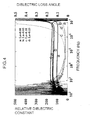
- Fig. 4 shows a frequency dependence of a relative dielectric constant and a dielectric loss angle (tan ⁇ ) of the BFO-containing ferroelectric material of the embodiment.
- a solid line a in Fig. 4 indicates the relative dielectric constant, and a broken line a indicates the dielectric loss angle.
- the abscissa represents a frequency in the unit of "Hz". It can be seen that the relative dielectric constant is about 100 in the frequency range from 1 kHz to 10 MHz.
- the relative dielectric constant of single crystal BiFeO 3 of the rhombohedral system is about 45 at a frequency of 10 kHz. It can be understood from these results that the BFO-containing ferroelectric material of the embodiment is apparently distinguished from BiFeO 3 of the rhombohedral system.
- BFO-containing ferroelectric material can be obtained which has remanent polarization larger than 6.1 ⁇ C/cm 2 .
- Such a large remanent polarization cannot be obtained by conventional BiFeO 3 of the rhombohedral system.
- crystallization annealing temperature may be set to 400 °C to 650 °C.
- crystallization annealing is performed in the nitrogen atmosphere, it may be performed in other non-oxidizing atmospheres to form oxygen defects.
- BiFeO 3-x formed by the embodiment method has a higher empty lattice defect density of oxygen than that of the rhombohedral system. These defects cause an increase in leak current.
- dopant may be added.
- a rare earth element preferably La or Nd
- an increase in leak current can be suppressed.
- the rare earth element such as La and Nd
- some Bi elements are replaced with La or Nd.
- the parameter y is preferably set as 0.05 ⁇ y ⁇ 0.2 where the composition ratio of Bi is 1 - y and the composition ratio of La or Nd is y.
- the dopant is added to the precursor solution.
- Fig. 4 shows the relative dielectric constant and dielectric loss angle of Bi 1-y La y FeO 3-x added with La.
- Solid lines b, c and d indicate the relative dielectric constants at the La composition ratios y of 0.05, 0.10 and 0.15, respectively.
- Broken lines b, c and d indicate the dielectric loss angles at the La composition ratios y of 0.05, 0.10 and 0.15, respectively.
- Fig. 5 shows the relative dielectric constant and dielectric loss angle of Bi 1-y Nd y FeO 3-x added with Nd.
- Solid lines a, b and c indicate the relative dielectric constants at the La composition ratios y of 0.05, 0.10 and 0.15, respectively.
- Broken lines a, b and c indicate the dielectric loss angles at the Nd composition ratios y of 0.05, 0.10 and 0.15, respectively.
- a relative dielectric constant of 100 to 200 is obtained in the frequency range from 1 kHz to 10 MHz.
- a relative dielectric constant of PZT is about 800 and a relative dielectric constant of BLT is about 300.
- the relative dielectric constant of a ferroelectric film is preferably small in order to apply as large a portion as possible of the gate voltage, across the lamination structure of a gate insulating film and a ferroelectric film of one-transistor type FRAM, to the ferroelectric film.
- the relative dielectric constants of BiFeO 3-x doped with La or Nd and undoped BiFeO 3-x are larger than those of PZT and BLT.
- Ferroelectric material having a relative dielectric constant of 300 or smaller can be obtained. It can be said that as compared to PZT and BLT, this ferroelectric material is suitable for one-transistor type FRAM.
- Fig. 6 is a cross sectional view of one-transistor type FRAM according to an embodiment.
- a gate insulating film 105 On the surface of a channel region 102 of a silicon substrate 101, a gate insulating film 105, a floating gate electrode 106, a ferroelectric film 107 and a control gate electrode 108 are laminated in this order.
- a source region 103 and a drain region 104 are formed in the substrate surface layer on both sides of the channel region 102.
- the ferroelectric film 107 is made of the BFO-containing ferroelectric material of the tetragonal or orthorhombic system described in the above embodiment.
- the ferroelectric film 107 As a voltage is applied across the silicon substrate 101 and control gate 108, the ferroelectric film 107 is polarized. When the applied voltage is changed to 0 V thereafter, the remanent polarization is left in the ferroelectric film 107.
- the threshold value of FET changes depending on changes in the magnitude and direction of the remanent polarization.
- One-bit information can be stored by relating the magnitude of drain current changed with the threshold value to information "0" and "1". In the embodiment shown in Fig.
- the floating gate electrode 106 is formed, this may be omitted to form an MFIS-FET structure including the laminated structure of a control gate electrode (M), a ferroelectric film (F), a gate insulating film (I) and a semiconductor substrate (S) formed with a channel region.
- M control gate electrode
- F ferroelectric film
- I gate insulating film
- S semiconductor substrate
- an element isolation insulating film 201 is formed on the surface of a silicon substrate 200 by local oxidation of silicon (LOCOS), shallow trench isolation (STI) or the like.
- the element isolation insulating film 201 defines active regions.
- a MOSFET (switching element) 202 is formed in an active region.
- MOSFET 202 is constituted of a source region 202S, a drain region 202D, a gate insulating film 202I and a gate electrode 202G.
- An interlayer insulating film 205 of silicon oxide is formed covering MOSFET 202. After the surface of the interlayer insulating film 205 is planarized, via holes are formed through the interlayer insulating film 205 at positions corresponding to the source region 202S and drain region 202D. The via holes are filled with conductive plugs 206 and 207 of tungsten or the like. The conductive plugs 206 and 207 are connected to the source region 202S and drain region 202D, respectively.
- a protective film 210 of silicon nitride is formed on the interlayer insulating film 205.
- a Ti film 211 of 60 nm in thickness and a Pt film 212 of 150 nm in thickness are formed in this order by sputtering on the protective film 210.
- a BFO-containing ferroelectric film 213 of 300 nm in thickness is formed by the embodiment method described with Fig. 1.
- a Pt film 214 of 100 nm in thickness is formed by electron beam deposition.
- the Pt film 214 is patterned to form an upper electrode film 214a of Pt.
- the BFO-containing ferroelectric film 213 is patterned to form a capacitor dielectric film 213a.
- the two layers, Pt film 212 and Ti film 211, are patterned to form a lower electrode 215 of the two-layer structure.
- a capacitor 218 is formed being constituted of the lower electrode film 215, capacitor dielectric film 213a and upper electrode film 214a.
- An interlayer insulating film 220 is formed on the protective film 210, burying the capacitor 210. The surface of the interlayer insulating film is planarized.
- via holes are formed in and through the interlayer insulating film 220 and protective film 210 at predetermined positions, and filled with conductive plugs 222, 223 and 224 of tungsten or the like.
- the conductive plugs 222 and 223 are connected to the underlying conductive plugs 206 and 207, respectively.
- the conductive plug 224 is connected to the upper electrode layer 214a.
- an Al wiring 230 is formed interconnecting the conductive plugs 223 and 224.
- the drain region 202D is therefore connected to the upper electrode layer 214a of the capacitor 218 via the conductive plugs 207 and 223, wiring 230 and conductive plug 224.
- An interlayer insulating film 232 of silicon oxide is formed on the interlayer insulating film 220, covering the wiring 230.
- a via hole is formed through the interlayer insulating film 232 at a predetermined position, and filled with a conductive plug 233 of tungsten.
- an Al wiring 235 is formed connected to the conductive plug 233.
- the source region 202S is therefore connected to the wiring 235 via the conductive plugs 206, 222 and 233.
- the BFO-containing ferroelectric material of the tetragonal or orthorhombic system described with Fig. 1 is used, so that a lead-free FRAM can be manufactured.
- the material of the ferroelectric film of FRAM presents remanent polarization equivalent to that of PZT.
Landscapes
- Chemical & Material Sciences (AREA)
- Engineering & Computer Science (AREA)
- Mechanical Engineering (AREA)
- Metallurgy (AREA)
- General Chemical & Material Sciences (AREA)
- Chemical Kinetics & Catalysis (AREA)
- Physics & Mathematics (AREA)
- Materials Engineering (AREA)
- Inorganic Chemistry (AREA)
- Thermal Sciences (AREA)
- Organic Chemistry (AREA)
- Ceramic Engineering (AREA)
- Semiconductor Memories (AREA)
- Compositions Of Oxide Ceramics (AREA)
- Non-Volatile Memory (AREA)
- Inorganic Insulating Materials (AREA)
Abstract
Description
- The present invention relates to a ferroelectric material, a manufacturing method thereof, and ferroelectric memories, and more particularly to those in which the ferroelectric material contains Bi, Fe and O as constituent elements.
- Non-volatile memories having a capacitor dielectric film made of ferroelectric material with spontaneous polarization have drawn attention as next generation memories, called FRAM, and applications to non-contact IC cards or the like are expected. One-transistor type FRAM (1T-FRAM) and one-transistor - one-capacitor type FRAM are known, the former having a ferroelectric film deposited on the gate insulating film of FET and the latter having a capacitor dielectric film of DRAM replaced with a ferroelectric film.
- Usable known ferroelectric material includes material having a perovskite structure such as Pb(Zr, Ti) O3 (PZT) and material having a bismuth layer-structured ferroelectric such as (Bi, La)4Ti3O12 (BLT) and SrBi2Ta2O9. Since the bismuth layer-structured ferroelectric does not contain lead, contrary to PZT, this material is suitable in terms of environmental contamination. Although BLT has remanent polarization to generally the same degree as PZT, it is difficult to form a capacitor dielectric film with orientation having the maximum remanent polarization in a thickness direction. If a capacitor dielectric film is formed by using BLT, the actual remanent polarization is likely to be smaller than the maximum remanent polarization specific to the material.
- In a one-transistor type FRAM, two layers consisting of a gate insulating film and a ferroelectric film are inserted between a channel and a gate electrode. In order to apply a voltage efficiently to a ferroelectric film, it is desired to lower a relative dielectric constant of the ferroelectric film as much as possible. Japanese Patent Laid-open Publication No. 2001-210794 discloses FRAM made of ferroelectric material BiFeO3 which does not contain lead.
- As compared to PZT, however, BiFeO3 has a small remanent polarization.
- It is therefore desirable to provide ferroelectric material which does not contain lead and presents remanent polarization to generally the same degree as PZT, and a method of manufacturing the same.
- It is also desirable to provide a ferroelectric memory using such ferroelectric material.
- According to one aspect of the present invention, there is provided a ferroelectric material containing constituent elements of Bi, Fe and O and having crystal lattice of a tetragonal or orthorhombic system.
- According to another aspect of the present invention, there is provided a ferroelectric material containing constituent elements of Bi, Fe and O and having remanent polarization larger than 6.1 µC/cm2.
- According to still another aspect of the present invention, there is provided a ferroelectric material containing constituent elements of Bi, Fe and O and having a relative dielectric constant equal to or larger than 100 and equal to or smaller than 300.
- According to still another aspect of the present invention, there is provided a ferroelectric material containing constituent elements of Bi, Fe and O wherein when an X-ray diffraction pattern is measured, first and second peaks are observed, the first peak corresponding to (101) and (011) planes and the second peak corresponding to (110) plane being separated from the first peak.
- According to still another aspect of the present invention, there is provided a method of manufacturing a ferroelectric film comprising steps of: (a) coating BiFeO3 precursor solution on a surface of an underlying member; (b) performing heat treatment after the coating to form a dielectric film; and (c) heating the dielectric film in a non-oxidizing atmosphere to crystallize the dielectric film.
- According to still another aspect of the present invention, there is provided a ferroelectric memory using the above-described ferroelectric material.
- As a crystal lattice of the BFO-containing ferroelectric material containing Bi, Fe and O as constituent elements is changed from a conventional rhombohedral system to the tetragonal or orthorhombic system, large remanent polarization can be obtained. Although the remanent polarization of single crystal BiFeO3 of the rhombohederal system is 6.1 µC/cm2, remanent polarization larger than this can be obtained by changing the lattice structure to the tetragonal or orthorhombic system.
- A relative dielectric constant of 300 or smaller is smaller than a relative dielectric constant of PZT, which is about 800. Ferroelectric material having a small relative dielectric constant is suitable for the ferroelectric film material of a one-transistor type FRAM. When an X-ray diffraction pattern of a crystal lattice of the tetragonal system is measured, first and second peaks are observed, the first peak corresponding to (101) and (011) planes and the second peak corresponding to (110) plane being separated from the first peak. Even in the orthorhombic system, the peak corresponding to the (101) plane is generally superposed upon the peak corresponding to the (011) plane if a difference between a-axis and b-axis lengths is small.
- As BiFeO3 of the rhombohedral system is subjected to heat treatment in a non-oxidizing atmosphere, oxygen is partially eliminated and oxygen detects are formed. As the oxygen defects are introduced, the crystal lattice changes to the tetragonal or orthorhombic system.
- Reference will now be made, by way of example, to the accompanying drawings in which:
- Fig. 1 is a cross sectional view of a capacitor made of BiFeO-containing ferroelectric material according to an embodiment.
- Fig. 2 is a graph showing an X-ray diffraction pattern of BiFeO-containing ferroelectric material.
- Fig. 3 is a graph showing a P-E hysteresis loop of BiFeO-containing ferroelectric material according to the embodiment.
- Fig. 4 is a graph showing the frequency dependency of the relative dielectric constant and dielectric loss angle δ of BiFeO-containing ferroelectric material and BiFeO-containing ferroelectric material which contains La.
- Fig. 5 is a graph showing the frequency dependency of the relative dielectric constant and dielectric loss angle δ of BiFeO-containing ferroelectric material which contains Nd.
- Fig. 6 is a cross sectional view of one-transistor type FRAM.
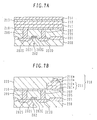
- Figs. 7A to 7C are cross sectional views of one-transistor - one-capacitor type FRAM during and after manufacture.
- Fig. 1 is a cross sectional view of a capacitor made of ferroelectric material according to an embodiment. On the surface of a substrate 1 made of n-type silicon, a
silicon oxide film 2 is formed. For example, thesilicon oxide film 2 is formed by thermal oxidation. Alower electrode film 3, a capacitordielectric film 5 and anupper electrode film 6 are formed in this order on thesilicon oxide film 2. Thelower electrode film 3 has a two-layer structure of a Ti film 3a having a thickness of 60 nm and aPt film 3b having a thickness of 100 nm. For example, the Ti film 3a andPt film 3b can be formed by sputtering. - The capacitor
dielectric film 5 is formed, for example, by chemical solution deposition (CSD). This film forming procedure will be described in the following. Precursor solution of BiFeO3 is spin-coated on thelower electrode 3. For example, solvent for this precursor solution is 2-methoxyethanol, and the concentration of BiFeO3 is 0.15 mol%. The substrate is placed on a hot plate for one minute at a temperature of 150 °C to evaporate the solvent. After evaporating the solvent, the substrate is placed on a hot plate at a temperature of 400 °C to perform pyrolysis. After the pyrolysis, the substrate is cooled down to room temperature. A BiFeO3 film is therefore obtained in an amorphous or crystalline state. A series of processes including precursor solution coating, solvent evaporation, pyrolysis and cooling is repeated, for example, 32 times. The number of repetitions is adjusted in accordance with a desired film thickness. - By using a rapid thermal annealing (RTA) system and raising the temperature to 500 °C in 20 seconds in a nitrogen gas atmosphere, heat treatment (crystallization annealing) is performed for 5 minutes. With this heat treatment, BiFeO3 is crystallized and oxygen is partially eliminated so that oxygen defects (oxygen empty lattice points) occur. BiFeO3 with oxygen defects is denoted as BiFeO3-x. Ferroelectric material which contains Bi, Fe and O as constituent elements, such as BiFeO3 and BiFeO3-x, is called BFO-containing ferroelectric material. A film thickness of BiFeO3-x after crystallization is, for example, 300 nm.
- On the crystallized capacitor
dielectric film 5, theupper electrode film 6 of Pt is formed by vacuum deposition using a metal mask. A capacitor is therefore formed having the capacitordielectric film 5 made of BFO-containing ferroelectric material with oxygen defects and sandwiched between thelower electrode film 3 andupper electrode film 6. - For comparison, a ferroelectric film was formed which was made of BFO-containing ferroelectric material whose crystallization annealing was performed in an oxidizing atmosphere.
- Fig. 2 shows the comparison between an X-ray diffraction pattern (solid line a) of BFO-containing ferroelectric material according to the embodiment and an X-ray diffraction pattern (solid line b) of BFO-containing ferroelectric material according to the comparative example. The BFO-containing ferroelectric material of the comparative example has a broad peak corresponding to the (012) plane, indicating that the material has a crystal lattice of the rhombohedral system.
- The BFO-containing ferroelectric material of the embodiment has a relatively high peak corresponding to the (101) plane and a relatively low peak corresponding to the (110) plane. If crystal is of the cubic system, all the (110), (101) and (011) planes are equivalent so that the peaks corresponding to these planes will not be separated. In the BFO-containing ferroelectric material of the embodiment, the peak corresponding to the (101) plane superposes upon the peak corresponding to the (011) plane, and its height is about twice the peak corresponding to the (110) plane. Namely, the crystal lattice of this BFO-containing ferroelectric material can be considered almost the tetragonal system. It can be considered that since BiFeO3 is annealed in the nitrogen atmosphere, oxygen defects are formed and crystal of almost the tetragonal system is formed.
- Crystal of the tetragonal system has the same a-axis and b-axis length of the crystal lattice, and the c-axis length is different from the a-axis length. If the a-axis length is different from the b-axis length, i.e., if crystal is of the orthorhombic system, the peak corresponding to the (101) plane is separated from the peak corresponding to the (011) plane. However, if a difference between the a-axis length and b-axis length is small, the two peaks are not separated clearly, and are observed like one peak. It can therefore be considered from the X-ray diffraction results shown in Fig. 2 that the BFO-containing ferroelectric material of the embodiment is of the tetragonal system or of the orthorhombic system having such a small difference between the a-axis length and b-axis length as unable to be detected through X-ray diffraction.
- Fig. 3 shows a P-E hysteresis loop of the capacitor dielectric film of the embodiment. The abscissa represents an applied electric field in the unit of "kV/cm" and the ordinate represents the magnitude of polarization in the unit of "µC/cm2". A large hysteresis having a magnitude of remanent polarization of 30 µC/cm2 or larger appears. The magnitude of this remanent polarization is about the same degree as that of remanent polarization of PZT. It is known that remanent polarization of single crystal BiFeO3 of the rhombohedral system is 6.1 µC/cm2. If the crystal lattice of BFO-containing ferroelectric material is changed from the rhombohedral system to the tetragonal or orthorhombic system, remanent polarization can be made large.
- Fig. 4 shows a frequency dependence of a relative dielectric constant and a dielectric loss angle (tan δ) of the BFO-containing ferroelectric material of the embodiment. A solid line a in Fig. 4 indicates the relative dielectric constant, and a broken line a indicates the dielectric loss angle. The abscissa represents a frequency in the unit of "Hz". It can be seen that the relative dielectric constant is about 100 in the frequency range from 1 kHz to 10 MHz. The relative dielectric constant of single crystal BiFeO3 of the rhombohedral system is about 45 at a frequency of 10 kHz. It can be understood from these results that the BFO-containing ferroelectric material of the embodiment is apparently distinguished from BiFeO3 of the rhombohedral system.
- With the above-described embodiment method, BFO-containing ferroelectric material can be obtained which has remanent polarization larger than 6.1 µC/cm2. Such a large remanent polarization cannot be obtained by conventional BiFeO3 of the rhombohedral system.
- In the above-described embodiment, although crystallization annealing is performed at 500 °C, the crystallization annealing temperature may be set to 400 °C to 650 °C.
- Also in the above-described embodiment, although crystallization annealing is performed in the nitrogen atmosphere, it may be performed in other non-oxidizing atmospheres to form oxygen defects.
- BiFeO3-x formed by the embodiment method has a higher empty lattice defect density of oxygen than that of the rhombohedral system. These defects cause an increase in leak current. In order to suppress an increase in leak current, dopant may be added. By adding, as dopant, a rare earth element, preferably La or Nd, an increase in leak current can be suppressed. As the rare earth element such as La and Nd is added, some Bi elements are replaced with La or Nd. In order to obtain the leak current increase suppressing effects, the parameter y is preferably set as 0.05 ≤ y ≤ 0.2 where the composition ratio of Bi is 1 - y and the composition ratio of La or Nd is y. The dopant is added to the precursor solution.
- Fig. 4 shows the relative dielectric constant and dielectric loss angle of Bi1-yLayFeO3-x added with La. Solid lines b, c and d indicate the relative dielectric constants at the La composition ratios y of 0.05, 0.10 and 0.15, respectively. Broken lines b, c and d indicate the dielectric loss angles at the La composition ratios y of 0.05, 0.10 and 0.15, respectively.
- Fig. 5 shows the relative dielectric constant and dielectric loss angle of Bi1-yNdyFeO3-x added with Nd. Solid lines a, b and c indicate the relative dielectric constants at the La composition ratios y of 0.05, 0.10 and 0.15, respectively. Broken lines a, b and c indicate the dielectric loss angles at the Nd composition ratios y of 0.05, 0.10 and 0.15, respectively.
- In both cases, a relative dielectric constant of 100 to 200 is obtained in the frequency range from 1 kHz to 10 MHz. A relative dielectric constant of PZT is about 800 and a relative dielectric constant of BLT is about 300. The relative dielectric constant of a ferroelectric film is preferably small in order to apply as large a portion as possible of the gate voltage, across the lamination structure of a gate insulating film and a ferroelectric film of one-transistor type FRAM, to the ferroelectric film. The relative dielectric constants of BiFeO3-x doped with La or Nd and undoped BiFeO3-x are larger than those of PZT and BLT. Ferroelectric material having a relative dielectric constant of 300 or smaller can be obtained. It can be said that as compared to PZT and BLT, this ferroelectric material is suitable for one-transistor type FRAM.
- Fig. 6 is a cross sectional view of one-transistor type FRAM according to an embodiment. On the surface of a
channel region 102 of asilicon substrate 101, agate insulating film 105, a floatinggate electrode 106, aferroelectric film 107 and acontrol gate electrode 108 are laminated in this order. Asource region 103 and adrain region 104 are formed in the substrate surface layer on both sides of thechannel region 102. Theferroelectric film 107 is made of the BFO-containing ferroelectric material of the tetragonal or orthorhombic system described in the above embodiment. - As a voltage is applied across the
silicon substrate 101 andcontrol gate 108, theferroelectric film 107 is polarized. When the applied voltage is changed to 0 V thereafter, the remanent polarization is left in theferroelectric film 107. The threshold value of FET changes depending on changes in the magnitude and direction of the remanent polarization. One-bit information can be stored by relating the magnitude of drain current changed with the threshold value to information "0" and "1". In the embodiment shown in Fig. 6, although the floatinggate electrode 106 is formed, this may be omitted to form an MFIS-FET structure including the laminated structure of a control gate electrode (M), a ferroelectric film (F), a gate insulating film (I) and a semiconductor substrate (S) formed with a channel region. - With reference to Figs. 7A to 7C, description will be made of a method of manufacturing one-transistor - one-capacitor type FRAM.
- As shown in Fig. 7A, an element
isolation insulating film 201 is formed on the surface of asilicon substrate 200 by local oxidation of silicon (LOCOS), shallow trench isolation (STI) or the like. The elementisolation insulating film 201 defines active regions. In an active region, a MOSFET (switching element) 202 is formed.MOSFET 202 is constituted of a source region 202S, a drain region 202D, a gate insulating film 202I and a gate electrode 202G. - An interlayer insulating
film 205 of silicon oxide is formed coveringMOSFET 202. After the surface of theinterlayer insulating film 205 is planarized, via holes are formed through theinterlayer insulating film 205 at positions corresponding to the source region 202S and drain region 202D. The via holes are filled withconductive plugs - A
protective film 210 of silicon nitride is formed on theinterlayer insulating film 205. ATi film 211 of 60 nm in thickness and aPt film 212 of 150 nm in thickness are formed in this order by sputtering on theprotective film 210. On thePt film 212, a BFO-containingferroelectric film 213 of 300 nm in thickness is formed by the embodiment method described with Fig. 1. On the BFO-containingferroelectric film 213, aPt film 214 of 100 nm in thickness is formed by electron beam deposition. - As shown in Fig. 7B, the
Pt film 214 is patterned to form an upper electrode film 214a of Pt. The BFO-containingferroelectric film 213 is patterned to form a capacitor dielectric film 213a. The two layers,Pt film 212 andTi film 211, are patterned to form alower electrode 215 of the two-layer structure. In this manner, acapacitor 218 is formed being constituted of thelower electrode film 215, capacitor dielectric film 213a and upper electrode film 214a. An interlayer insulatingfilm 220 is formed on theprotective film 210, burying thecapacitor 210. The surface of the interlayer insulating film is planarized. - As shown in Fig. 7C, via holes are formed in and through the
interlayer insulating film 220 andprotective film 210 at predetermined positions, and filled withconductive plugs conductive plugs conductive plug 224 is connected to the upper electrode layer 214a. - On the
interlayer insulating film 220, anAl wiring 230 is formed interconnecting theconductive plugs capacitor 218 via theconductive plugs wiring 230 andconductive plug 224. - An interlayer insulating
film 232 of silicon oxide is formed on theinterlayer insulating film 220, covering thewiring 230. A via hole is formed through theinterlayer insulating film 232 at a predetermined position, and filled with aconductive plug 233 of tungsten. On theinterlayer insulating film 232, anAl wiring 235 is formed connected to theconductive plug 233. The source region 202S is therefore connected to thewiring 235 via the conductive plugs 206, 222 and 233. - As the material of a capacitor dielectric film, the BFO-containing ferroelectric material of the tetragonal or orthorhombic system described with Fig. 1 is used, so that a lead-free FRAM can be manufactured. The material of the ferroelectric film of FRAM presents remanent polarization equivalent to that of PZT.
- The present invention has been described in connection with the preferred embodiments. The invention is not limited only to the above embodiments. It will be apparent to those skilled in the art that other various modifications, improvements, combinations, and the like can be made.
Claims (12)
- A ferroelectric material containing constituent elements of Bi, Fe and O and having crystal lattice of a tetragonal or orthorhombic system.
- A ferroelectric material containing constituent elements of Bi, Fe and O and having remanent polarization larger than 6.1 µC/cm2.
- A ferroelectric material containing constituent elements of Bi, Fe and O and having a relative dielectric constant equal to or larger than 100 and equal to or smaller than 300.
- A ferroelectric material containing constituent elements of Bi, Fe and O wherein as an X-ray diffraction pattern is measured, first and second peaks are observed, the first peak corresponding to (101) and (011) planes and the second peak corresponding to (110) plane being separated from the first peak.
- The ferroelectric material of claim 1, 2, 3, or 4, wherein the ferroelectric material has a composition of BiFeO3 with oxygen defects.
- The ferroelectric material of any of claims 1-5, further comprising a rare earth element.
- The ferroelectric material according to claim 6, wherein y is 0.05 ≤ y ≤ 0.2 where a Bi composition ratio is 1 - y and a rare earth element composition ratio is y.
- The ferroelectric material according to claim 6 or 7, wherein the rare earth element is La or Nd.
- A method of manufacturing a ferroelectric film comprising steps of:(a) coating BiFeO3 precursor solution on a surface of an underlying member;(b) performing heat treatment after the coating to form a dielectric film; and(c) heating the dielectric film in a non-oxidizing atmosphere to crystallize the dielectric film.
- The method of manufacturing a ferroelectric film according to claim 9, wherein a heating temperature at the step (c) is 400 °C to 650 °C.
- A ferroelectric memory comprising:a semiconductor substrate;source and drain regions formed in a surface layer of the semiconductor substrate and disposed on both sides of a channel region;a gate insulating film formed on the channel region and including a film made of a ferroelectric material containing constituent elements of Bi, Fe and O and having crystal lattice of a tetragonal or orthorhombic system.
- A ferroelectric memory comprising:a switching element formed on a semiconductor substrate for switching a current path between a pair of terminals; anda capacitor connected to one terminal of the switching element and including a capacitor dielectric film made of a ferroelectric material containing constituent elements of Bi, Fe and O and having crystal lattice of a tetragonal or orthorhombic system.
Applications Claiming Priority (1)
| Application Number | Priority Date | Filing Date | Title |
|---|---|---|---|
| JP2004371905A JP2006176366A (en) | 2004-12-22 | 2004-12-22 | Ferroelectric material, method for manufacturing the same, and ferroelectric memory |
Publications (1)
| Publication Number | Publication Date |
|---|---|
| EP1675161A1 true EP1675161A1 (en) | 2006-06-28 |
Family
ID=35840175
Family Applications (1)
| Application Number | Title | Priority Date | Filing Date |
|---|---|---|---|
| EP05007865A Withdrawn EP1675161A1 (en) | 2004-12-22 | 2005-04-11 | Ferroelectric material, manufacturing method and ferroelectric memory |
Country Status (3)
| Country | Link |
|---|---|
| US (1) | US20060131627A1 (en) |
| EP (1) | EP1675161A1 (en) |
| JP (1) | JP2006176366A (en) |
Families Citing this family (20)
| Publication number | Priority date | Publication date | Assignee | Title |
|---|---|---|---|---|
| JP4693634B2 (en) * | 2006-01-17 | 2011-06-01 | 株式会社東芝 | Spin FET |
| JP5041121B2 (en) * | 2006-04-12 | 2012-10-03 | セイコーエプソン株式会社 | Inkjet recording head and inkjet printer |
| JP5041120B2 (en) * | 2006-04-12 | 2012-10-03 | セイコーエプソン株式会社 | Inkjet recording head and inkjet printer |
| US8179025B1 (en) * | 2008-02-29 | 2012-05-15 | University Of Maryland College Park | Lead-free piezoceramic materials |
| JP5267971B2 (en) * | 2008-03-21 | 2013-08-21 | 国立大学法人金沢大学 | Ferroelectric material and piezoelectric material |
| US8591987B2 (en) * | 2009-05-18 | 2013-11-26 | Northrop Grumman Systems Corporation | Multiferroic nanoscale thin film materials, method of its facile syntheses and magnetoelectric coupling at room temperature |
| US9356224B2 (en) * | 2009-10-30 | 2016-05-31 | The Regents Of The University Of California | Thin film bismuth iron oxides useful for piezoelectric devices |
| JP5577844B2 (en) | 2009-11-02 | 2014-08-27 | セイコーエプソン株式会社 | Liquid ejector |
| JP2011207202A (en) | 2009-11-02 | 2011-10-20 | Seiko Epson Corp | Liquid-ejecting head, liquid-ejecting apparatus, piezoelectric element, and piezoelectric material |
| JP5621964B2 (en) | 2009-11-02 | 2014-11-12 | セイコーエプソン株式会社 | Liquid ejecting head, liquid ejecting apparatus, piezoelectric element, and ultrasonic device |
| JP5660274B2 (en) * | 2010-01-05 | 2015-01-28 | セイコーエプソン株式会社 | Liquid ejecting head manufacturing method, piezoelectric element manufacturing method, liquid ejecting head, liquid ejecting apparatus, and piezoelectric element |
| WO2011091709A1 (en) * | 2010-01-28 | 2011-08-04 | 复旦大学 | Ferro-resistive random access memory (ferro-rram), operation method and manufacturing mehtod thereof |
| US8416609B2 (en) | 2010-02-15 | 2013-04-09 | Micron Technology, Inc. | Cross-point memory cells, non-volatile memory arrays, methods of reading a memory cell, methods of programming a memory cell, methods of writing to and reading from a memory cell, and computer systems |
| US8437174B2 (en) | 2010-02-15 | 2013-05-07 | Micron Technology, Inc. | Memcapacitor devices, field effect transistor devices, non-volatile memory arrays, and methods of programming |
| US8634224B2 (en) | 2010-08-12 | 2014-01-21 | Micron Technology, Inc. | Memory cells, non-volatile memory arrays, methods of operating memory cells, methods of writing to and reading from a memory cell, and methods of programming a memory cell |
| JP2012085234A (en) * | 2010-10-14 | 2012-04-26 | Ngk Spark Plug Co Ltd | Transmission system and transmission apparatus |
| FR3009433B1 (en) * | 2013-08-01 | 2015-09-11 | St Microelectronics Crolles 2 | BACKLIGHT ILLUMINATION IMAGE SENSOR WITH LOW DARK CURRENT |
| KR20210149162A (en) * | 2019-04-08 | 2021-12-08 | 케플러 컴퓨팅 인크. | Doped polar layer and semiconductor device comprising same |
| CN110550954A (en) * | 2019-09-18 | 2019-12-10 | 昆明贵研新材料科技有限公司 | Core-shell lanthanum-doped bismuth ferrite/silicon dioxide composite ceramic and preparation method thereof |
| KR102944589B1 (en) * | 2021-09-17 | 2026-03-25 | 삼성전자주식회사 | Ferroelectric semiconductor device and method for extracting defect density of the same |
Citations (2)
| Publication number | Priority date | Publication date | Assignee | Title |
|---|---|---|---|---|
| JP2001210794A (en) * | 2000-01-27 | 2001-08-03 | Seiko Epson Corp | Ferroelectric memory material |
| US20020025637A1 (en) * | 2000-08-24 | 2002-02-28 | Secretary Of Agency Of Industrial Science And Technology | Method for manufacturing self-matching transistor |
-
2004
- 2004-12-22 JP JP2004371905A patent/JP2006176366A/en not_active Withdrawn
-
2005
- 2005-04-11 EP EP05007865A patent/EP1675161A1/en not_active Withdrawn
- 2005-04-15 US US11/106,529 patent/US20060131627A1/en not_active Abandoned
Patent Citations (2)
| Publication number | Priority date | Publication date | Assignee | Title |
|---|---|---|---|---|
| JP2001210794A (en) * | 2000-01-27 | 2001-08-03 | Seiko Epson Corp | Ferroelectric memory material |
| US20020025637A1 (en) * | 2000-08-24 | 2002-02-28 | Secretary Of Agency Of Industrial Science And Technology | Method for manufacturing self-matching transistor |
Non-Patent Citations (5)
| Title |
|---|
| GABBASOVA Z.V. ET AL.: "Bi1-xRxFeO3 (R=rare earth): a family of novel magnetoelectrics", PHYSICS LETTERS A, vol. 158, no. 9, 23 September 1991 (1991-09-23), North-Holland, pages 491 - 498, XP002370020 * |
| PATENT ABSTRACTS OF JAPAN vol. 2000, no. 25 12 April 2001 (2001-04-12) * |
| YUN K. Y., NODA M. ET AL.: "Effects of annealing atmosphere on crystallization and electrical properties in BiFeO3 thin films by chemical solution deposition (CSD)", JOURNAL OF THE KOREAN PHYSICAL SOCIETY, vol. 42, April 2003 (2003-04-01), pages S1153 - S1156, XP008060754 * |
| YUN K. Y., RICINSCHI D. ET AL.: "Giant ferroelectric polarization beyond 150 ?C/cm2 in BiFeO3 thin film", JAPANESE JOURNAL OF APPLIED PHYSICS, vol. 43, no. 5A, 1 May 2004 (2004-05-01), pages L647 - L648, XP002370019 * |
| YUN KWI ET AL: "Structural and multiferroic properties of BiFeO3 thin films at room temperature", JOURNAL OF APPLIED PHYSICS, AMERICAN INSTITUTE OF PHYSICS. NEW YORK, US, vol. 96, no. 6, 15 September 2004 (2004-09-15), pages 3399 - 3403, XP012068829, ISSN: 0021-8979 * |
Also Published As
| Publication number | Publication date |
|---|---|
| JP2006176366A (en) | 2006-07-06 |
| US20060131627A1 (en) | 2006-06-22 |
Similar Documents
| Publication | Publication Date | Title |
|---|---|---|
| EP1675161A1 (en) | Ferroelectric material, manufacturing method and ferroelectric memory | |
| US7964904B2 (en) | Semiconductor device and method of manufacturing the same | |
| US6649954B2 (en) | Ferroelectric capacitor having upper electrode lamination | |
| US6608383B2 (en) | Semiconductor device including capacitor with lower electrode including iridium and iridium oxide layers | |
| US8153448B2 (en) | Manufacturing method of a semiconductor device | |
| KR100334353B1 (en) | Method of fabricating ferroelectric integrated circuit using oxygen to inhibit and repair hydrogen degradation | |
| US8236643B2 (en) | Method of manufacturing semiconductor device including ferroelectric capacitor | |
| US8110411B2 (en) | Semiconductor device and manufacturing method thereof | |
| JPH10189906A (en) | Capacitor structure of semiconductor memory cell and method of manufacturing the same | |
| US20090127603A1 (en) | Semiconductor memory device and manufacturing method thereof | |
| JP2000208725A (en) | Semiconductor device and method of manufacturing semiconductor device | |
| JP2002530862A (en) | Inert gas recovery annealing of hydrogen damaged ferroelectric films | |
| KR20020035620A (en) | Integrated circuits with barrier layers and methods of fabricating same | |
| US7459361B2 (en) | Semiconductor device with ferroelectric capacitor and fabrication method thereof | |
| JP2007088147A (en) | Semiconductor device and manufacturing method thereof | |
| JP4657545B2 (en) | Manufacturing method of semiconductor device | |
| JP2003179212A (en) | Capacitor, memory element and method of manufacturing the same | |
| JP3914171B2 (en) | Semiconductor device and manufacturing method thereof | |
| EP1077478A2 (en) | Method of making ferroelectric thin film, ferroelectric capacitor, ferroelectric memory and method for fabricating ferroelectric memory | |
| JP2009224668A (en) | Semiconductor device and manufacturing method therefor | |
| JPH11307733A (en) | Manufacturing method of ferroelectric integrated circuit | |
| JP2000012708A (en) | Semiconductor device and manufacturing method thereof | |
| JPH10150158A (en) | Method for manufacturing capacitor structure of semiconductor memory cell | |
| JP2005072029A (en) | Method for forming crystallized film and method for manufacturing semiconductor device | |
| KR20010018258A (en) | Method for Manufacturing Ferroelectric Memory Device having Improved Barrier Layer with Rapid Thermal Annealing |
Legal Events
| Date | Code | Title | Description |
|---|---|---|---|
| PUAI | Public reference made under article 153(3) epc to a published international application that has entered the european phase |
Free format text: ORIGINAL CODE: 0009012 |
|
| AK | Designated contracting states |
Kind code of ref document: A1 Designated state(s): AT BE BG CH CY CZ DE DK EE ES FI FR GB GR HU IE IS IT LI LT LU MC NL PL PT RO SE SI SK TR |
|
| AX | Request for extension of the european patent |
Extension state: AL BA HR LV MK YU |
|
| 17P | Request for examination filed |
Effective date: 20060719 |
|
| AKX | Designation fees paid |
Designated state(s): DE FR GB IT |
|
| 17Q | First examination report despatched |
Effective date: 20070305 |
|
| STAA | Information on the status of an ep patent application or granted ep patent |
Free format text: STATUS: THE APPLICATION IS DEEMED TO BE WITHDRAWN |
|
| 18D | Application deemed to be withdrawn |
Effective date: 20090407 |