EP1672374A1 - Acceleration sensor - Google Patents
Acceleration sensor Download PDFInfo
- Publication number
- EP1672374A1 EP1672374A1 EP05255452A EP05255452A EP1672374A1 EP 1672374 A1 EP1672374 A1 EP 1672374A1 EP 05255452 A EP05255452 A EP 05255452A EP 05255452 A EP05255452 A EP 05255452A EP 1672374 A1 EP1672374 A1 EP 1672374A1
- Authority
- EP
- European Patent Office
- Prior art keywords
- support portion
- weight
- substrate
- detection element
- acceleration sensor
- Prior art date
- Legal status (The legal status is an assumption and is not a legal conclusion. Google has not performed a legal analysis and makes no representation as to the accuracy of the status listed.)
- Withdrawn
Links
Images


Classifications
-
- G—PHYSICS
- G01—MEASURING; TESTING
- G01P—MEASURING LINEAR OR ANGULAR SPEED, ACCELERATION, DECELERATION, OR SHOCK; INDICATING PRESENCE, ABSENCE, OR DIRECTION, OF MOVEMENT
- G01P15/00—Measuring acceleration; Measuring deceleration; Measuring shock, i.e. sudden change of acceleration
- G01P15/02—Measuring acceleration; Measuring deceleration; Measuring shock, i.e. sudden change of acceleration by making use of inertia forces using solid seismic masses
- G01P15/08—Measuring acceleration; Measuring deceleration; Measuring shock, i.e. sudden change of acceleration by making use of inertia forces using solid seismic masses with conversion into electric or magnetic values
- G01P15/12—Measuring acceleration; Measuring deceleration; Measuring shock, i.e. sudden change of acceleration by making use of inertia forces using solid seismic masses with conversion into electric or magnetic values by alteration of electrical resistance
-
- G—PHYSICS
- G01—MEASURING; TESTING
- G01P—MEASURING LINEAR OR ANGULAR SPEED, ACCELERATION, DECELERATION, OR SHOCK; INDICATING PRESENCE, ABSENCE, OR DIRECTION, OF MOVEMENT
- G01P15/00—Measuring acceleration; Measuring deceleration; Measuring shock, i.e. sudden change of acceleration
- G01P15/18—Measuring acceleration; Measuring deceleration; Measuring shock, i.e. sudden change of acceleration in two or more dimensions
-
- G—PHYSICS
- G01—MEASURING; TESTING
- G01P—MEASURING LINEAR OR ANGULAR SPEED, ACCELERATION, DECELERATION, OR SHOCK; INDICATING PRESENCE, ABSENCE, OR DIRECTION, OF MOVEMENT
- G01P1/00—Details of instruments
- G01P1/02—Housings
- G01P1/023—Housings for acceleration measuring devices
-
- G—PHYSICS
- G01—MEASURING; TESTING
- G01P—MEASURING LINEAR OR ANGULAR SPEED, ACCELERATION, DECELERATION, OR SHOCK; INDICATING PRESENCE, ABSENCE, OR DIRECTION, OF MOVEMENT
- G01P15/00—Measuring acceleration; Measuring deceleration; Measuring shock, i.e. sudden change of acceleration
- G01P15/02—Measuring acceleration; Measuring deceleration; Measuring shock, i.e. sudden change of acceleration by making use of inertia forces using solid seismic masses
- G01P15/08—Measuring acceleration; Measuring deceleration; Measuring shock, i.e. sudden change of acceleration by making use of inertia forces using solid seismic masses with conversion into electric or magnetic values
- G01P15/12—Measuring acceleration; Measuring deceleration; Measuring shock, i.e. sudden change of acceleration by making use of inertia forces using solid seismic masses with conversion into electric or magnetic values by alteration of electrical resistance
- G01P15/123—Measuring acceleration; Measuring deceleration; Measuring shock, i.e. sudden change of acceleration by making use of inertia forces using solid seismic masses with conversion into electric or magnetic values by alteration of electrical resistance by piezo-resistive elements, e.g. semiconductor strain gauges
-
- G—PHYSICS
- G01—MEASURING; TESTING
- G01P—MEASURING LINEAR OR ANGULAR SPEED, ACCELERATION, DECELERATION, OR SHOCK; INDICATING PRESENCE, ABSENCE, OR DIRECTION, OF MOVEMENT
- G01P15/00—Measuring acceleration; Measuring deceleration; Measuring shock, i.e. sudden change of acceleration
- G01P15/02—Measuring acceleration; Measuring deceleration; Measuring shock, i.e. sudden change of acceleration by making use of inertia forces using solid seismic masses
- G01P15/08—Measuring acceleration; Measuring deceleration; Measuring shock, i.e. sudden change of acceleration by making use of inertia forces using solid seismic masses with conversion into electric or magnetic values
- G01P2015/0805—Measuring acceleration; Measuring deceleration; Measuring shock, i.e. sudden change of acceleration by making use of inertia forces using solid seismic masses with conversion into electric or magnetic values being provided with a particular type of spring-mass-system for defining the displacement of a seismic mass due to an external acceleration
- G01P2015/0822—Measuring acceleration; Measuring deceleration; Measuring shock, i.e. sudden change of acceleration by making use of inertia forces using solid seismic masses with conversion into electric or magnetic values being provided with a particular type of spring-mass-system for defining the displacement of a seismic mass due to an external acceleration for defining out-of-plane movement of the mass
- G01P2015/084—Measuring acceleration; Measuring deceleration; Measuring shock, i.e. sudden change of acceleration by making use of inertia forces using solid seismic masses with conversion into electric or magnetic values being provided with a particular type of spring-mass-system for defining the displacement of a seismic mass due to an external acceleration for defining out-of-plane movement of the mass the mass being suspended at more than one of its sides, e.g. membrane-type suspension, so as to permit multi-axis movement of the mass
-
- H—ELECTRICITY
- H10—SEMICONDUCTOR DEVICES; ELECTRIC SOLID-STATE DEVICES NOT OTHERWISE PROVIDED FOR
- H10W—GENERIC PACKAGES, INTERCONNECTIONS, CONNECTORS OR OTHER CONSTRUCTIONAL DETAILS OF DEVICES COVERED BY CLASS H10
- H10W72/00—Interconnections or connectors in packages
- H10W72/50—Bond wires
- H10W72/531—Shapes of wire connectors
- H10W72/536—Shapes of wire connectors the connected ends being ball-shaped
-
- H—ELECTRICITY
- H10—SEMICONDUCTOR DEVICES; ELECTRIC SOLID-STATE DEVICES NOT OTHERWISE PROVIDED FOR
- H10W—GENERIC PACKAGES, INTERCONNECTIONS, CONNECTORS OR OTHER CONSTRUCTIONAL DETAILS OF DEVICES COVERED BY CLASS H10
- H10W72/00—Interconnections or connectors in packages
- H10W72/50—Bond wires
- H10W72/531—Shapes of wire connectors
- H10W72/5363—Shapes of wire connectors the connected ends being wedge-shaped
-
- H—ELECTRICITY
- H10—SEMICONDUCTOR DEVICES; ELECTRIC SOLID-STATE DEVICES NOT OTHERWISE PROVIDED FOR
- H10W—GENERIC PACKAGES, INTERCONNECTIONS, CONNECTORS OR OTHER CONSTRUCTIONAL DETAILS OF DEVICES COVERED BY CLASS H10
- H10W72/00—Interconnections or connectors in packages
- H10W72/50—Bond wires
- H10W72/551—Materials of bond wires
- H10W72/552—Materials of bond wires comprising metals or metalloids, e.g. silver
- H10W72/5522—Materials of bond wires comprising metals or metalloids, e.g. silver comprising gold [Au]
Definitions
- the present invention relates to an acceleration sensor and, more particularly, to a semiconductor acceleration sensor with improved shock resistance.
- a variety of devices for detecting this stress or acceleration have been conventionally developed, of which one device is known in which a gauge resistor is formed on a semiconductor substrate as a detection element and which converts the mechanical strain produced on the basis of a force acting on the substrate that is supplied from outside into an electrical signal as a result of the piezoresistive effect ("Development of three-weight sensor" 'Invention' Journal pages 52 to 63, published by the Invention Society on September 2003).
- the characteristic of the invention that is described in "Development of three weight sensor" 'Invention' Journal pages 52 to 63, published by the Invention Society on September 2003, is the fact that it is possible, by means of force sensors for a plurality of axial directions formed on a semiconductor substrate, to constitute sensors of a plurality of types, that is, sensors of four types, namely, a three-axis force sensor, a three-axis acceleration sensor, a three-axis angular speed sensor, and a six-axis motion sensor by means of one device.
- an acceleration sensor with a structure in which the relationship between the weight and support portion is reversed that is, in which the support portion is placed in the center of the acceleration sensor and the weight is suspended by means of a beam portion at the periphery of the support portion, is known.
- an acceleration sensor with this structure is expediently referred to as a parasol-type acceleration sensor.
- an acceleration sensor having a structure in which the support portion is placed in the center, that is, a parasol-type acceleration sensor, such that there is no damage to the acceleration sensor even when the product on which the acceleration sensor is mounted is dropped or a strong shock is applied.
- a first aspect of the present invention provides an acceleration sensor that comprises a support portion the lower end of which is fixed to a substrate; a beam portion on which a detection element for applying changes to an output signal in correspondence with strain caused by acceleration acting on the detection element is formed, one end of the beam portion being connected to the top (upper) part of the support portion; a suspended weight connected to the other end of the beam portion; and a stopper substrate with a window portion through which, in order to guide an output signal of the detection element via a pad that is formed on the upper end face of the support portion, a conductor lead that is connected to the pad passes, wherein the stopper substrate is fixed, e.g. by means of adhesive, to a region surrounding the pad of the upper end face of the support portion and upward overswing of the weight is limited by means of the stopper substrate.
- a second aspect of the present invention provides an acceleration sensor that comprises a support portion the lower end of which is fixed to a substrate and the upper end face of which comprises a pad; four beam portions, a respective one end of each of which is connected to the upper end portion of the support portion in an orthogonal direction with the support portion at the center and on which a detection element that applies changes to the output signal in correspondence with strain caused by acceleration acting on the detection element is formed; a suspended weight connected to the other end of each of the four beam portions; a support-portion extension part disposed between two adjacent beam portions of the four beam portions; and a stopper substrate with a window portion through which, in order to guide an output signal of the detection element via a pad that is formed on the upper end face of the support portion, a conductor lead that is connected to the pad passes, wherein the stopper substrate is fixed, e.g. by means of adhesive, to the extension part of the support portion and limits upward overswing of the weight.
- a third aspect of the present invention provides an acceleration sensor that comprises a support portion the lower end of which is fixed to a substrate and the upper end face of which comprises a pad; four beam portions, a respective one end of each of which is connected to the upper end portion of the support portion in an orthogonal direction with the support portion at the center and on which a detection element that applies changes to the output signal in correspondence with strain caused by acceleration acting on the detection element is formed; a suspended weight connected to the other end of each of the four beam portions; a support-portion extension part that is disposed between two adjacent beam portions of the four beam portions; and a stopper substrate with a window portion through which, in order to guide an output signal of the detection element via a pad that is formed on the extension part of the support portion, a conductor lead that is connected to the pad passes, wherein the stopper substrate is fixed, e.g. by means of adhesive, to the upper end face of the support portion and limits upward overswing of the weight.
- a fourth aspect of the present invention provides an acceleration sensor that comprises a support portion the lower end of which is fixed to a substrate; a beam portion on which a detection element for applying changes to an output signal in correspondence with strain caused by acceleration acting on the detection element is formed, one end of the beam portion being connected to the top part of the support portion; a suspended weight connected to the other end of the beam portion; a stopper substrate with a window portion through which, in order to guide an output signal of the detection element via a pad that is formed on the upper end face of the support portion, a conductor lead that is connected to the pad passes; and a frame portion that surrounds the weight, wherein the stopper substrate is fixed, e.g. by means of adhesive, to the upper end face of the frame portion and limits upward overswing of the weight.
- the support portion, beam portion and weight are integrally formed from a semiconductor substrate.
- the support portion, beam portion, weight and frame portion are integrally formed from a semiconductor substrate and the weight and frame portion are connected by means of a join portion and the frame portion is separated from the weight by cutting the join portion after mounting in a package.
- the acceleration sensor further comprises a groove between the extension of the support portion and the pad formed on the upper end face of the support portion.
- the interval between the weight and the stopper substrate is 2 to 12 ⁇ m.
- an acceleration sensor in which the shock resistance is improved at low cost and which exhibits high connection reliability.
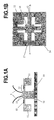
- Fig. 1 shows a parasol type acceleration sensor chip.
- Fig. 1A is a cross sectional view and Fig. 1B is an upper (plan) view. Further, the cross sectional view of Fig. 1A is a cross sectional view along the line A-B in Fig. 1B.
- the acceleration sensor chip comprises a support portion 10 that is fixed to the center of a substrate 16, and a weight 11 that is disposed at the periphery of the support portion 10.
- the weight 11 is linked to, and suspended by means of, beam portions (detection beam) 12, one end of each of which is connected to the top part (upper end) of the support portion 10.
- beam portions detection beam
- Each beam portion 12 is flexible so that when a stress or acceleration is applied, the beam portions 12 may strain.
- the support portion 10, weight 11, and beam portion 12 are integrally formed by machining a semiconductor substrate by means of micromachine technology.
- a detection element 13 that applies changes to an output signal in correspondence with the strain caused by the acceleration acting on the weight 11 is formed on the top (upper) part of at least some of the beam portions 12.
- the substrate 16 fulfils the role of a stopper for the downward movement of the weight 11.
- a plurality of bonding pads 14 are provided on the upper end face of the support portion 10, as shown in Fig. 1B.
- the bonding pads 14 are electrically connected by means of leads (not shown) to the detection elements 13.
- the bonding pads 14 are connected by means of a metal wire 5 or similar to an external lead out terminal that is formed on the side of the package (not illustrated).
- the present invention proposes a structure to help resolve this problem.
- Fig. 2 shows a structure of a first embodiment of an acceleration sensor of the present invention.
- Fig. 2A is a cross sectional view of the first embodiment
- Fig. 2B is an upper (plan) view in which the acceleration sensor chip (the part circled by a broken line 2 in Fig. 2A) housed within the package is observed with the upper stopper substrate 15 (shown in Fig. 2C) removed
- Fig. 2D is an upper (plan) view of a state where the upper stopper substrate 15 is present.
- Fig. 2A is a cross sectional view along the broken line A-B in Fig. 2B.
- the package is formed in multiple layers (three layers in this embodiment) by means of ceramic material.
- the acceleration sensor chip 2 is housed in a package and the acceleration sensor chip 2 comprises a support portion 10 that is centrally fixed to the substrate 16, and a weight 11 that is disposed at the periphery of the support portion 10.
- the weight 11 is linked to and suspended by means of beam portions (detection beam) 12, one end of each of which is connected to the top part (upper end) of the support portion 10.
- the support portion 10, weight 11 and beam portions 12 are integrally formed out of a semiconductor substrate by means of micromachine technology.
- Detection elements 13 that apply changes to the output signal in correspondence with the strain caused by an acceleration acting on the weight 11 are formed on the top (upper) parts of at least some of the beam portions 12.
- the substrate 16 fulfils the role of a stopper for the downward movement of the weight 11.
- the substrate 16 is also fixed to the inside bottom face of the package by means of adhesive 17.
- a plurality of bonding pads 14 are provided on the upper end face of the support portion 10, as shown in Fig. 28.
- the bonding pads 14 are electrically connected by means of leads (not shown) to the detection elements 13.
- bonding pads 14 are connected by means of metal wires 5 or similar to the external lead out terminals 4 that are formed on the side of the package (not illustrated).
- Each external lead out terminal 4 is also connected to an electrode terminal 18 that is formed on the package bottom face by means of an electrically conductive film that is formed along the package wall.
- Each electrode terminal 18 is soldered to the required circuit parts of the substrate when the acceleration sensor is mounted on the circuit substrate.
- the acceleration sensor of the first embodiment further comprises an upper stopper substrate 15 that fulfils the role of a stopper for the upward movement of the weight 11.
- the upper stopper substrate 15 is bonded by means of adhesive 15b, formed to surround the plurality of bonding pads 14, to the upper end face of the support portion 10.
- Fig. 2C is a plan view of the upper stopper substrate 15 that fulfils the role of a stopper to limit the overswing of the upward movement of the weight 11.
- the upper stopper substrate 15 comprises a window portion 15a at the center thereof. Therefore, the connecting wires 5 are able to connect the bonding pads 14 and external lead out terminals 4 via the window portion 15a of the upper stopper substrate 15.
- Fig. 3 shows the structure of a second embodiment of the present invention.
- Fig. 3A is a cross sectional view of the second embodiment
- Fig. 3B is an upper (plan) view in which the acceleration sensor chip (part circled by the broken line marked 2 in Fig. 3A) housed in the package is observed with the upper stopper substrate 15 (shown in Fig. 3C) removed
- Fig. 3D is an upper (plan) view of a state where the upper stopper substrate 15 is provided.
- the cross-sectional view of Fig. 3A is a view along the broken line A-B in Fig. 3B.
- the package is formed in three layers by means of ceramic material similarly to the example in Fig. 2.
- the acceleration sensor chip 2 is housed in a package and the acceleration sensor chip 2 comprises a support portion 10 that is centrally fixed to the substrate 16, and a weight 11 that is disposed at the periphery of the support portion 10.
- the weight 11 is linked to the other end of each of beam portions (detection beam) 12, one end of each of which is connected to the top (upper) part of the support portion 10.
- the support portion 10, weight 11 and beam portions 12 are integrally formed from a semiconductor substrate by means of micromachine technology.
- Detection elements 13 that apply changes to the output signal in correspondence with the strain caused by the acceleration acting on the weight 11 are formed on the top (upper) part of at least some of the beam portions 12.
- the substrate 16 fulfils the role of a stopper for the downward movement of the weight 11.
- the substrate 16 is also fixed to the inside bottom face of the package by means of adhesive 17.
- a plurality of bonding pads 14 are provided on the upper end face of the support portion 10, as shown in Fig. 3B.
- the bonding pads 14 are electrically connected by means of leads (not shown) to the detection elements 13.
- the bonding pads 14 are also connected by means of metal wires 5 or similar to external lead out terminals 4 that are formed on the side of the package.
- Each external lead out terminal 4 is connected to an electrode terminal 18 that is formed on the package bottom face by means of an electrically conductive film that is formed along the package wall.
- the electrode terminal 18 is soldered to the required circuit parts of the substrate when the acceleration sensor is mounted on the circuit substrate.
- the acceleration sensor further comprises a stopper substrate 15 that fulfils the role of a stopper for the upward movement of the weight 11.
- the weight 11 forms a substantially square frame shape with four sides, the center of each of the four sides being connected to the other end of a beam portion (detection beam) 12 and linked to the middle support portion 10.
- the middle support portion 10 comprises extension parts 11a to 11d of the support portion that extend in oblique directions at an angle to (diagonally from) the beam portion (detection beam) 12.
- the upper stopper substrate 15 is bonded by means of adhesive 15b to extension parts 11a to 11d of the support portion 10.
- Fig. 3C is a planar view of the upper stopper substrate 15 that fulfils the role of a stopper to limit the overswing of the upward movement of the weight 11.
- the upper stopper substrate 15 comprises a window portion 15a at the center thereof. Therefore, the connecting wires 5 are able to connect the bonding pads 14 and external lead out terminals 4 via the window portion 15a of the upper stopper substrate 15.
- the second embodiment shown in Fig. 3 is a constitution in which the upper stopper substrate 15 is bonded at four points spaced apart from the plurality of bonding pads 14, whereby the bonding strength can be increased and the flow of adhesive 15b to the bonding pads 14 can be prevented. Deterioration of the electrical connection can therefore be prevented.
- Fig. 4 shows the structure of a third embodiment of the present invention.
- Fig. 4A is a cross-sectional view of the third embodiment
- Fig. 4B is an upper (plan) view in which the acceleration sensor chip (part circled by the broken line portion 2 in Fig. 4A) housed in the package is observed with the upper stopper substrate 15 (shown in Fig. 4C) removed
- Fig. 4D is an upper (plan) view of a state where the upper stopper substrate 15 is provided.
- the cross sectional view of Fig. 4A is a view along the broken line A-B in Fig. 4B.
- the package is formed in three layers by means of ceramic material similarly to the earlier embodiments in Figs. 2 and 3.
- the acceleration sensor chip 2 is housed in a package and the acceleration sensor chip 2 comprises a support portion 10 that is centrally fixed to the substrate 16, and a weight 11 that is disposed at the periphery of the support portion 10.
- the weight 11 is linked to and suspended from beam portions (detection beam) 12, one end of each of which is connected to the top (upper) part of the support portion 10.
- the support portion 10, weight 11 and beam portions 12 are integrally formed from a semiconductor substrate by means of micromachine technology.
- Detection elements 13 that apply changes to the output signal in correspondence with the strain caused by the acceleration acting on the weight 11 are formed on the top (upper) part of the beam portion 12.
- the substrate 16 fulfils the role of a stopper for overswing of the downward movement of the weight 11.
- the substrate 16 is also fixed to the inside bottom face of the package by means of adhesive 17.
- the acceleration sensor further comprises a stopper substrate 15 that fulfils the role of a stopper for the upward movement of the weight 11.
- the weight 11 forms a substantially square frame shape with four sides, the center of each of the four sides being connected to the other end of the beam portions (detection beam) 12 and linked to the middle support portion 10.
- the middle support portion 10 comprises extension parts 11a to 11d of the support portion that extend in an oblique direction at an angle to the beam portion (detection beam) 12.
- the difference of the third embodiment from the second embodiment shown in Fig. 3 is the position of the plurality of bonding pads 14. That is, in the embodiment shown in Fig. 4, the plurality of bonding pads 14 are arranged on four extension parts 11a to 11d of the extended support portion. Therefore, the upper stopper substrate 15 comprises four window portions 15a for connecting lead-out wires such as the metal wires 5 to the bonding pads 14 in correspondence with the four extension parts 11a to 11d respectively.
- the upper stopper substrate 15 is connected to the support portion 10 by means of adhesive 15b that is formed on the upper end (surface) of the support portion 10.
- the bonding pads 14 are in positions spaced apart from the center and, therefore, the length of lead-out wires such as the metal wires 5 for connection with the external lead-out terminals 4 may be made shorter than in the case of the first and second embodiments, whereby reliability can be increased.
- Fig. 5 illustrates a fourth embodiment of the present invention.
- Fig. 5A is a cross-sectional view of the fourth embodiment
- Fig.5B is an upper (plan) view in which the acceleration sensor chip (part circled by the broken line portion 2 in Fig. 5A) housed in the package is observed with the upper stopper substrate le (shown in Fig. 5C) removed
- Fig. 5D is an upper view of a state where the upper stopper substrate 15 is provided.
- the cross-sectional view of Fig. 5A is a view along the broken line A B in Fig. 5.
- This embodiment is a constitution in which a frame 19 for holding the upper stopper substrate 15 is provided independently of the acceleration sensor chip 2.
- the upper stopper substrate 15 comprises a window portion 15a through which lead out wire such as the metal wire 5 for connecting the bonding pads 14 and external lead out terminals 4 are passed as per the other embodiments.
- the window portion 15a forms a square in this embodiment but may also form another shape such as a circle, for example.
- the plurality of bonding pads 14 is formed on the end (upper) face of the support portion 10 similarly to the first and second embodiment. However, the bonding pads 14 may also be formed on each of the four extension parts 11a to 11d as per the third embodiment.
- Fig. 6 illustrates the constitution of the fabrication process for the acceleration sensor chip 2 and frame 19 of the embodiment in Fig. 5.
- the acceleration sensor chip 2 and frame 19 can be fabricated by cutting them, from a semiconductor substrate by means of micromachine technology. Thus, machining is performed by leaving parts 20a to 20d that link the parts of the frame 19 and acceleration sensor chip 2.
- the frame 19 is afforded a structure that is produced by fixing the frame 19 to the upper stopper substrate 15 or substrate 16 through bonding and then cutting the frame 19 from the body of the acceleration sensor chip by means of a laser.
- Fig. 7 is a modified example of the embodiment shown in Fig. 3.
- grooves 21 are formed between the adhesive 15b, for fixing the upper stopper substrate 15, formed on the four extension parts 11a to 11d and the bonding pads 14.
- the risk of adhesive 15b flowing to the area of the bonding pads 14 can be avoided. Accordingly, an acceleration sensor with superior shock resistance and with which electrical connection reliability is high can be provided.
- Fig. 8 illustrates a gap G between the weight 11 and upper stopper substrate 15 of an acceleration sensor common to each embodiment. It is possible to limit the upward movement of the weight 11 by making the gap G approximately 2 to 12 ⁇ m by means of the adhesive 15b or by inserting a spacer. As a result, the reliability of the shock resistance can be improved.
- the present invention makes it possible to provide an acceleration sensor with superior shock resistance by means of a simple constitution. It is thus possible to provide highly reliable electronic devices by installing an acceleration sensor embodying the present invention.
Landscapes
- Physics & Mathematics (AREA)
- General Physics & Mathematics (AREA)
- Pressure Sensors (AREA)
Abstract
Description
- The present invention relates to an acceleration sensor and, more particularly, to a semiconductor acceleration sensor with improved shock resistance.
- In order to implement various types of control in moving bodies such as automobiles and ships, and in robots, mechanical fabrication devices, or mobile devices that are grasped and used by a user, such as notebook PCs, portable telephones, PDA (Personal Digital Assistant), DVC (Digital Video Camera), DSC (Digital Still Camera), for example, it is essential to detect the stress acting on all or part of the target body in correspondence with the objective of the control. By sensing the stress on the basis of the acceleration acting on all or part of the target, it is possible to sense the acceleration.
- A variety of devices for detecting this stress or acceleration have been conventionally developed, of which one device is known in which a gauge resistor is formed on a semiconductor substrate as a detection element and which converts the mechanical strain produced on the basis of a force acting on the substrate that is supplied from outside into an electrical signal as a result of the piezoresistive effect ("Development of three-weight sensor" 'Invention' Journal pages 52 to 63, published by the Invention Society on September 2003).
- In addition, the fact that it is also possible to use a change in the electrostatic capacity corresponding with strain instead of using the piezoresistive effect of the gauge resistor is explained in "Development of three weight sensor" 'Invention' Journal pages 52 to 63, published by the Invention Society on September 2003.
- In particular, the characteristic of the invention that is described in "Development of three weight sensor" 'Invention' Journal pages 52 to 63, published by the Invention Society on September 2003, is the fact that it is possible, by means of force sensors for a plurality of axial directions formed on a semiconductor substrate, to constitute sensors of a plurality of types, that is, sensors of four types, namely, a three-axis force sensor, a three-axis acceleration sensor, a three-axis angular speed sensor, and a six-axis motion sensor by means of one device.
- Proposals have been made to solve a variety of problems relating to a semiconductor acceleration sensor that employs the principles mentioned in "Development of three weight sensor" 'Invention' Journal pages 52 to 63, published by the Invention Society on September 2003. One of these various problems is that a large unforeseen shock can sometimes be applied as a result of the environment in which the acceleration sensor is used (depending on what kind of device the acceleration sensor is used in). In such a case, there is a risk that the weight will be displaced greatly and the gauge resistor will be damaged as a result.
- In order to eliminate this problem, a constitution in which a stopper that limits the displacement of the weight is provided has been proposed (Japanese Patent Application Laid Open No. 2000-304762).
- Here, as indicated in "Development of three weight sensor" 'Invention' Journal pages 52 to 63, published by the Invention Society on September 2003, and in Japanese Patent publication H8-7228, an acceleration sensor with a structure in which the relationship between the weight and support portion is reversed, that is, in which the support portion is placed in the center of the acceleration sensor and the weight is suspended by means of a beam portion at the periphery of the support portion, is known. In the following description, an acceleration sensor with this structure is expediently referred to as a parasol-type acceleration sensor.
- An acceleration sensor with a parasol-type acceleration sensor structure in which the support portion is placed in the center is illustrated in "Development of three-weight sensor" 'Invention' Journal pages 52 to 63, published by the Invention Society on September 2003, and Japanese Patent publication H8-7228. However, a parasol type acceleration sensor having a structure in which shocks to the acceleration sensor are limited has not been suggested or provided.
- Therefore, it is desirable to provide a structure with superior shock resistance for an acceleration sensor having a structure in which the support portion is placed in the center, that is, a parasol-type acceleration sensor, such that there is no damage to the acceleration sensor even when the product on which the acceleration sensor is mounted is dropped or a strong shock is applied.
- A first aspect of the present invention provides an acceleration sensor that comprises a support portion the lower end of which is fixed to a substrate; a beam portion on which a detection element for applying changes to an output signal in correspondence with strain caused by acceleration acting on the detection element is formed, one end of the beam portion being connected to the top (upper) part of the support portion; a suspended weight connected to the other end of the beam portion; and a stopper substrate with a window portion through which, in order to guide an output signal of the detection element via a pad that is formed on the upper end face of the support portion, a conductor lead that is connected to the pad passes, wherein the stopper substrate is fixed, e.g. by means of adhesive, to a region surrounding the pad of the upper end face of the support portion and upward overswing of the weight is limited by means of the stopper substrate.
- A second aspect of the present invention provides an acceleration sensor that comprises a support portion the lower end of which is fixed to a substrate and the upper end face of which comprises a pad; four beam portions, a respective one end of each of which is connected to the upper end portion of the support portion in an orthogonal direction with the support portion at the center and on which a detection element that applies changes to the output signal in correspondence with strain caused by acceleration acting on the detection element is formed; a suspended weight connected to the other end of each of the four beam portions; a support-portion extension part disposed between two adjacent beam portions of the four beam portions; and a stopper substrate with a window portion through which, in order to guide an output signal of the detection element via a pad that is formed on the upper end face of the support portion, a conductor lead that is connected to the pad passes, wherein the stopper substrate is fixed, e.g. by means of adhesive, to the extension part of the support portion and limits upward overswing of the weight.
- A third aspect of the present invention provides an acceleration sensor that comprises a support portion the lower end of which is fixed to a substrate and the upper end face of which comprises a pad; four beam portions, a respective one end of each of which is connected to the upper end portion of the support portion in an orthogonal direction with the support portion at the center and on which a detection element that applies changes to the output signal in correspondence with strain caused by acceleration acting on the detection element is formed; a suspended weight connected to the other end of each of the four beam portions; a support-portion extension part that is disposed between two adjacent beam portions of the four beam portions; and a stopper substrate with a window portion through which, in order to guide an output signal of the detection element via a pad that is formed on the extension part of the support portion, a conductor lead that is connected to the pad passes, wherein the stopper substrate is fixed, e.g. by means of adhesive, to the upper end face of the support portion and limits upward overswing of the weight.
- A fourth aspect of the present invention provides an acceleration sensor that comprises a support portion the lower end of which is fixed to a substrate; a beam portion on which a detection element for applying changes to an output signal in correspondence with strain caused by acceleration acting on the detection element is formed, one end of the beam portion being connected to the top part of the support portion; a suspended weight connected to the other end of the beam portion; a stopper substrate with a window portion through which, in order to guide an output signal of the detection element via a pad that is formed on the upper end face of the support portion, a conductor lead that is connected to the pad passes; and a frame portion that surrounds the weight, wherein the stopper substrate is fixed, e.g. by means of adhesive, to the upper end face of the frame portion and limits upward overswing of the weight.
- According to an embodiment of any of the first to third aspects, the support portion, beam portion and weight are integrally formed from a semiconductor substrate.
- According to an embodiment of the acceleration sensor according to the fourth aspect, the support portion, beam portion, weight and frame portion are integrally formed from a semiconductor substrate and the weight and frame portion are connected by means of a join portion and the frame portion is separated from the weight by cutting the join portion after mounting in a package.
- According to an embodiment of the second aspect, the acceleration sensor further comprises a groove between the extension of the support portion and the pad formed on the upper end face of the support portion.
- According to an embodiment of any of the first to seventh aspects, the interval between the weight and the stopper substrate is 2 to 12 µm.
- According to aspects of the present invention, it is possible to provide an acceleration sensor in which the shock resistance is improved at low cost and which exhibits high connection reliability.
- Reference will now be made, by way of example only, to the accompanying drawings, in which:
- Fig. 1 shows a parasol-type acceleration sensor chip;
- Fig. 2 shows a structure of a first embodiment of the present invention;
- Fig. 3 shows a structure of a second embodiment of the present invention;
- Fig. 4 shows a structure of a third embodiment of the present invention;
- Fig. 5 shows a structure of a fourth embodiment of the present invention;
- Fig. 6 illustrates the constitution of a fabrication process for an
acceleration sensor chip 2 and aframe 19 of the embodiment in Fig. 5; - Fig. 7 is a modified example of the embodiment shown in Fig. 3; and
- Fig. 8 illustrates a gap G between a
weight 11 and anupper stopper substrate 15 of an acceleration sensor common to each embodiment. - Embodiments of the present invention will be described hereinbelow with reference to the drawings.
- Fig. 1 shows a parasol type acceleration sensor chip.
- Fig. 1A is a cross sectional view and Fig. 1B is an upper (plan) view. Further, the cross sectional view of Fig. 1A is a cross sectional view along the line A-B in Fig. 1B.
- In Fig. 1, the acceleration sensor chip comprises a
support portion 10 that is fixed to the center of asubstrate 16, and aweight 11 that is disposed at the periphery of thesupport portion 10. - The
weight 11 is linked to, and suspended by means of, beam portions (detection beam) 12, one end of each of which is connected to the top part (upper end) of thesupport portion 10. Eachbeam portion 12 is flexible so that when a stress or acceleration is applied, thebeam portions 12 may strain. Thesupport portion 10,weight 11, andbeam portion 12 are integrally formed by machining a semiconductor substrate by means of micromachine technology. - A
detection element 13 that applies changes to an output signal in correspondence with the strain caused by the acceleration acting on theweight 11 is formed on the top (upper) part of at least some of thebeam portions 12. - Here, the
substrate 16 fulfils the role of a stopper for the downward movement of theweight 11. - A plurality of
bonding pads 14 are provided on the upper end face of thesupport portion 10, as shown in Fig. 1B. Thebonding pads 14 are electrically connected by means of leads (not shown) to thedetection elements 13. Thebonding pads 14 are connected by means of ametal wire 5 or similar to an external lead out terminal that is formed on the side of the package (not illustrated). - In the case of the acceleration sensor chip shown in Fig. 1, the downward movement of the
weight 11 is limited by means of thesubstrate 16 but the upward movement of theweight 11 is unrestricted. Therefore, when a large shock is applied to the acceleration sensor, there is the risk of damage to thebeam portions 12 as described earlier. - Therefore, the present invention proposes a structure to help resolve this problem.
- Fig. 2 shows a structure of a first embodiment of an acceleration sensor of the present invention. In Fig. 2, Fig. 2A is a cross sectional view of the first embodiment; Fig. 2B is an upper (plan) view in which the acceleration sensor chip (the part circled by a
broken line 2 in Fig. 2A) housed within the package is observed with the upper stopper substrate 15 (shown in Fig. 2C) removed; Fig. 2D is an upper (plan) view of a state where theupper stopper substrate 15 is present. Further, Fig. 2A is a cross sectional view along the broken line A-B in Fig. 2B. - In Fig. 2A, the package is formed in multiple layers (three layers in this embodiment) by means of ceramic material.
- The
acceleration sensor chip 2 is housed in a package and theacceleration sensor chip 2 comprises asupport portion 10 that is centrally fixed to thesubstrate 16, and aweight 11 that is disposed at the periphery of thesupport portion 10. Theweight 11 is linked to and suspended by means of beam portions (detection beam) 12, one end of each of which is connected to the top part (upper end) of thesupport portion 10. Thesupport portion 10,weight 11 andbeam portions 12 are integrally formed out of a semiconductor substrate by means of micromachine technology. -
Detection elements 13 that apply changes to the output signal in correspondence with the strain caused by an acceleration acting on theweight 11 are formed on the top (upper) parts of at least some of thebeam portions 12. - Here, the
substrate 16 fulfils the role of a stopper for the downward movement of theweight 11. Thesubstrate 16 is also fixed to the inside bottom face of the package by means of adhesive 17. - A plurality of
bonding pads 14 are provided on the upper end face of thesupport portion 10, as shown in Fig. 28. Thebonding pads 14 are electrically connected by means of leads (not shown) to thedetection elements 13. - In addition, the
bonding pads 14 are connected by means ofmetal wires 5 or similar to the external lead outterminals 4 that are formed on the side of the package (not illustrated). - Each external lead out terminal 4 is also connected to an
electrode terminal 18 that is formed on the package bottom face by means of an electrically conductive film that is formed along the package wall. Eachelectrode terminal 18 is soldered to the required circuit parts of the substrate when the acceleration sensor is mounted on the circuit substrate. - In addition, the acceleration sensor of the first embodiment further comprises an
upper stopper substrate 15 that fulfils the role of a stopper for the upward movement of theweight 11. Theupper stopper substrate 15 is bonded by means of adhesive 15b, formed to surround the plurality ofbonding pads 14, to the upper end face of thesupport portion 10. - Fig. 2C is a plan view of the
upper stopper substrate 15 that fulfils the role of a stopper to limit the overswing of the upward movement of theweight 11. Theupper stopper substrate 15 comprises awindow portion 15a at the center thereof. Therefore, the connectingwires 5 are able to connect thebonding pads 14 and external lead outterminals 4 via thewindow portion 15a of theupper stopper substrate 15. - Fig. 3 shows the structure of a second embodiment of the present invention. In Fig. 3, Fig. 3A is a cross sectional view of the second embodiment; Fig. 3B is an upper (plan) view in which the acceleration sensor chip (part circled by the broken line marked 2 in Fig. 3A) housed in the package is observed with the upper stopper substrate 15 (shown in Fig. 3C) removed; and Fig. 3D is an upper (plan) view of a state where the
upper stopper substrate 15 is provided. Further, the cross-sectional view of Fig. 3A is a view along the broken line A-B in Fig. 3B. - In Fig. 3A, the package is formed in three layers by means of ceramic material similarly to the example in Fig. 2.
- The
acceleration sensor chip 2 is housed in a package and theacceleration sensor chip 2 comprises asupport portion 10 that is centrally fixed to thesubstrate 16, and aweight 11 that is disposed at the periphery of thesupport portion 10. Theweight 11 is linked to the other end of each of beam portions (detection beam) 12, one end of each of which is connected to the top (upper) part of thesupport portion 10. Thesupport portion 10,weight 11 andbeam portions 12 are integrally formed from a semiconductor substrate by means of micromachine technology. -
Detection elements 13 that apply changes to the output signal in correspondence with the strain caused by the acceleration acting on theweight 11 are formed on the top (upper) part of at least some of thebeam portions 12. - The
substrate 16 fulfils the role of a stopper for the downward movement of theweight 11. Thesubstrate 16 is also fixed to the inside bottom face of the package by means of adhesive 17. - A plurality of
bonding pads 14 are provided on the upper end face of thesupport portion 10, as shown in Fig. 3B. Thebonding pads 14 are electrically connected by means of leads (not shown) to thedetection elements 13. - The
bonding pads 14 are also connected by means ofmetal wires 5 or similar to external lead outterminals 4 that are formed on the side of the package. - Each external lead out terminal 4 is connected to an
electrode terminal 18 that is formed on the package bottom face by means of an electrically conductive film that is formed along the package wall. Theelectrode terminal 18 is soldered to the required circuit parts of the substrate when the acceleration sensor is mounted on the circuit substrate. - Here, as with the first embodiment, the acceleration sensor further comprises a
stopper substrate 15 that fulfils the role of a stopper for the upward movement of theweight 11. In the second embodiment, theweight 11 forms a substantially square frame shape with four sides, the center of each of the four sides being connected to the other end of a beam portion (detection beam) 12 and linked to themiddle support portion 10. In addition, in comparison with the first embodiment in Fig. 2, in the case of the second embodiment, themiddle support portion 10 comprisesextension parts 11a to 11d of the support portion that extend in oblique directions at an angle to (diagonally from) the beam portion (detection beam) 12. - Furthermore, in this embodiment the
upper stopper substrate 15 is bonded by means of adhesive 15b toextension parts 11a to 11d of thesupport portion 10. Fig. 3C is a planar view of theupper stopper substrate 15 that fulfils the role of a stopper to limit the overswing of the upward movement of theweight 11. Similarly to the first embodiment, theupper stopper substrate 15 comprises awindow portion 15a at the center thereof. Therefore, the connectingwires 5 are able to connect thebonding pads 14 and external lead outterminals 4 via thewindow portion 15a of theupper stopper substrate 15. - In comparison with the first embodiment, the second embodiment shown in Fig. 3 is a constitution in which the
upper stopper substrate 15 is bonded at four points spaced apart from the plurality ofbonding pads 14, whereby the bonding strength can be increased and the flow of adhesive 15b to thebonding pads 14 can be prevented. Deterioration of the electrical connection can therefore be prevented. - Fig. 4 shows the structure of a third embodiment of the present invention. In Fig. 4, Fig. 4A is a cross-sectional view of the third embodiment; Fig. 4B is an upper (plan) view in which the acceleration sensor chip (part circled by the
broken line portion 2 in Fig. 4A) housed in the package is observed with the upper stopper substrate 15 (shown in Fig. 4C) removed; and Fig. 4D is an upper (plan) view of a state where theupper stopper substrate 15 is provided. Further, the cross sectional view of Fig. 4A is a view along the broken line A-B in Fig. 4B. - In Fig. 4A, the package is formed in three layers by means of ceramic material similarly to the earlier embodiments in Figs. 2 and 3.
- The
acceleration sensor chip 2 is housed in a package and theacceleration sensor chip 2 comprises asupport portion 10 that is centrally fixed to thesubstrate 16, and aweight 11 that is disposed at the periphery of thesupport portion 10. Theweight 11 is linked to and suspended from beam portions (detection beam) 12, one end of each of which is connected to the top (upper) part of thesupport portion 10. Thesupport portion 10,weight 11 andbeam portions 12 are integrally formed from a semiconductor substrate by means of micromachine technology. -
Detection elements 13 that apply changes to the output signal in correspondence with the strain caused by the acceleration acting on theweight 11 are formed on the top (upper) part of thebeam portion 12. - The
substrate 16 fulfils the role of a stopper for overswing of the downward movement of theweight 11. Thesubstrate 16 is also fixed to the inside bottom face of the package by means of adhesive 17. - Here, similarly to the earlier embodiments, the acceleration sensor further comprises a
stopper substrate 15 that fulfils the role of a stopper for the upward movement of theweight 11. Similarly to the second embodiment in Fig. 3, theweight 11 forms a substantially square frame shape with four sides, the center of each of the four sides being connected to the other end of the beam portions (detection beam) 12 and linked to themiddle support portion 10. In addition, themiddle support portion 10 comprisesextension parts 11a to 11d of the support portion that extend in an oblique direction at an angle to the beam portion (detection beam) 12. - The difference of the third embodiment from the second embodiment shown in Fig. 3 is the position of the plurality of
bonding pads 14. That is, in the embodiment shown in Fig. 4, the plurality ofbonding pads 14 are arranged on fourextension parts 11a to 11d of the extended support portion. Therefore, theupper stopper substrate 15 comprises fourwindow portions 15a for connecting lead-out wires such as themetal wires 5 to thebonding pads 14 in correspondence with the fourextension parts 11a to 11d respectively. - Furthermore, the
upper stopper substrate 15 is connected to thesupport portion 10 by means of adhesive 15b that is formed on the upper end (surface) of thesupport portion 10. - In the third embodiment, the
bonding pads 14 are in positions spaced apart from the center and, therefore, the length of lead-out wires such as themetal wires 5 for connection with the external lead-outterminals 4 may be made shorter than in the case of the first and second embodiments, whereby reliability can be increased. - Fig. 5 illustrates a fourth embodiment of the present invention. In Fig. 5, Fig. 5A is a cross-sectional view of the fourth embodiment; Fig.5B is an upper (plan) view in which the acceleration sensor chip (part circled by the
broken line portion 2 in Fig. 5A) housed in the package is observed with the upper stopper substrate le (shown in Fig. 5C) removed; and Fig. 5D is an upper view of a state where theupper stopper substrate 15 is provided. Further, the cross-sectional view of Fig. 5A is a view along the broken line A B in Fig. 5. - This embodiment is a constitution in which a
frame 19 for holding theupper stopper substrate 15 is provided independently of theacceleration sensor chip 2. As shown in Fig. SC, theupper stopper substrate 15 comprises awindow portion 15a through which lead out wire such as themetal wire 5 for connecting thebonding pads 14 and external lead outterminals 4 are passed as per the other embodiments. - The
window portion 15a forms a square in this embodiment but may also form another shape such as a circle, for example. In addition, in Fig. 5, the plurality ofbonding pads 14 is formed on the end (upper) face of thesupport portion 10 similarly to the first and second embodiment. However, thebonding pads 14 may also be formed on each of the fourextension parts 11a to 11d as per the third embodiment. - Fig. 6 illustrates the constitution of the fabrication process for the
acceleration sensor chip 2 andframe 19 of the embodiment in Fig. 5. Theacceleration sensor chip 2 andframe 19 can be fabricated by cutting them, from a semiconductor substrate by means of micromachine technology. Thus, machining is performed by leavingparts 20a to 20d that link the parts of theframe 19 andacceleration sensor chip 2. - Thereafter, the
frame 19 is afforded a structure that is produced by fixing theframe 19 to theupper stopper substrate 15 orsubstrate 16 through bonding and then cutting theframe 19 from the body of the acceleration sensor chip by means of a laser. As a result, collective die bonding of the external lead outterminals 4 ofpackage 1 andbonding pads 14 of the sensor chip is possible and an easily fabricated sensor with superior shock resistance can be provided. - Fig. 7 is a modified example of the embodiment shown in Fig. 3. In this example,
grooves 21 are formed between the adhesive 15b, for fixing theupper stopper substrate 15, formed on the fourextension parts 11a to 11d and thebonding pads 14. As a result of forming thesegrooves 21, the risk of adhesive 15b flowing to the area of thebonding pads 14 can be avoided. Accordingly, an acceleration sensor with superior shock resistance and with which electrical connection reliability is high can be provided. - Fig. 8 illustrates a gap G between the
weight 11 andupper stopper substrate 15 of an acceleration sensor common to each embodiment. It is possible to limit the upward movement of theweight 11 by making the gap G approximately 2 to 12 µm by means of the adhesive 15b or by inserting a spacer. As a result, the reliability of the shock resistance can be improved. - The present invention makes it possible to provide an acceleration sensor with superior shock resistance by means of a simple constitution. It is thus possible to provide highly reliable electronic devices by installing an acceleration sensor embodying the present invention.
Claims (10)
- An acceleration sensor, comprising:a support portion the lower end of which is fixed to a substrate;a beam portion on which a detection element is formed, the detection element for applying changes to an output signal in correspondence with strain caused by acceleration acting on the detection element, one end of the beam portion being connected to the upper end of the support portion;a suspended weight connected to the other end of the beam portion; anda stopper substrate having a window portion through which, in order to guide an output signal of the detection element via a pad that is formed on the upper end face of the support portion, a conductor lead that is connected to the pad passes,wherein the stopper substrate is fixed to a region of the upper end face of the support portion surrounding the pad and upward overswing of the weight is limited by means of the stopper substrate.
- An acceleration sensor, comprising:a support portion the lower end of which is fixed to a substrate and the upper end face of which includes a pad;four beam portions, one end of each of which being connected to the upper end portion of the support portion in an orthogonal direction with the support portion at the center and on at least one of which a detection element that applies changes to an output signal in correspondence with strain caused by acceleration acting on the detection element is formed;a suspended weight connected to the other ends of the four beam portions;a support-portion extension part disposed between two adjacent beam portions of the four beam portions; anda stopper substrate having a window portion through which, in order to guide an output signal of the detection element via a pad that is formed on the upper end face of the support portion, a conductor lead that is connected to the pad passes,wherein the stopper substrate is fixed to the extension part of the support portion and limits upward overswing of the weight.
- An acceleration sensor, comprising:a support portion the lower end of which is fixed to a substrate;four beam portions, one end of each of which is connected to the upper end portion of the support portion in an orthogonal direction with the support portion at the center and on at least one of which a detection element that applies changes to an output signal in correspondence with strain caused by acceleration acting on the detection element is formed;a suspended weight connected to the other ends of the four beam portions;a support-portion extension part that is disposed between two adjacent beam portions of the four beam portions; anda stopper substrate having a window portion through which, in order to guide an output signal of the detection element via a pad that is formed on the extension part of the support portion, a conductor lead that is connected to the pad passes,wherein the stopper substrate is fixed to the upper end face of the support portion and limits upward overswing of the weight.
- An acceleration sensor, comprising:a support portion the lower end of which is fixed to a substrate;a beam portion on which a detection element is formed, the detection element for applying changes to an output signal in correspondence with strain caused by acceleration acting on the detection element, one end of the beam portion being connected to the upper end of the support portion;a suspended weight connected to the other end of the beam portion;a stopper substrate having a window portion through which, in order to guide an output signal of the detection element via a pad that is formed on the upper end face of the support portion, a conductor lead that is connected to the pad passes; anda frame portion that surrounds the weight,wherein the stopper substrate is fixed to the upper end face of the frame portion and limits upward overswing of the weight.
- The acceleration sensor according to any of claims 1 to 3, wherein the support portion, beam portion and weight are integrally formed by means of a semiconductor substrate.
- The acceleration sensor according to claim 4, wherein the support portion, beam portion, weight and frame portion are integrally formed by means of a semiconductor substrate and the weight and frame portion are connected by means of a join portion and the frame portion is separated from the weight by cutting the join portion after mounting in a package.
- The acceleration sensor according to claim 2, further comprising:a groove between the extension of the support portion and the pad formed on the upper end face of the support portion.
- The acceleration sensor according to any of claims 1 to 7, wherein the interval between the weight and the stopper substrate is 2 to 12 µm.
- A method of fabricating an acceleration sensor, comprising steps of:cutting a support portion, beam portions, a weight and a frame portion from a semiconductor substrate such that the support portion, beam portions and weight are integrally formed and are linked to the frame portion by join portions;fixing the frame portion to a substrate through bonding; andcutting the join portions to separate the frame portion from the integrally formed support portion, beam portions and weight.
- An acceleration sensor, comprising:a support portion having a lower end fixed to a substrate;a weight;a beam portion connected at one end to an upper end of the support portion and at another end to the weight, which is suspended from the beam portion;a detection element formed on the beam portion for applying changes to an output signal in correspondence with strain caused by acceleration acting on the detection element; anda stopper substrate provided above the weight to limit upward overswing of the weight, the stopper substrate having a window portion through which a conductor lead carrying output signal passes.
Applications Claiming Priority (1)
| Application Number | Priority Date | Filing Date | Title |
|---|---|---|---|
| JP2004364927A JP2006170856A (en) | 2004-12-16 | 2004-12-16 | Acceleration sensor |
Publications (1)
| Publication Number | Publication Date |
|---|---|
| EP1672374A1 true EP1672374A1 (en) | 2006-06-21 |
Family
ID=36129956
Family Applications (1)
| Application Number | Title | Priority Date | Filing Date |
|---|---|---|---|
| EP05255452A Withdrawn EP1672374A1 (en) | 2004-12-16 | 2005-09-06 | Acceleration sensor |
Country Status (5)
| Country | Link |
|---|---|
| US (1) | US7296471B2 (en) |
| EP (1) | EP1672374A1 (en) |
| JP (1) | JP2006170856A (en) |
| KR (1) | KR20060069239A (en) |
| CN (1) | CN1790029A (en) |
Cited By (1)
| Publication number | Priority date | Publication date | Assignee | Title |
|---|---|---|---|---|
| CN108427010A (en) * | 2017-02-13 | 2018-08-21 | 精工爱普生株式会社 | Measuring physical and electronic equipment |
Families Citing this family (20)
| Publication number | Priority date | Publication date | Assignee | Title |
|---|---|---|---|---|
| JP2006119042A (en) * | 2004-10-22 | 2006-05-11 | Oki Electric Ind Co Ltd | Acceleration sensor chip package and manufacturing method thereof |
| JP4754817B2 (en) * | 2004-12-20 | 2011-08-24 | Okiセミコンダクタ株式会社 | Semiconductor acceleration sensor |
| JP2006284441A (en) * | 2005-04-01 | 2006-10-19 | Sharp Corp | Physical quantity sensor and detection method of physical quantity sensor |
| JP4949673B2 (en) * | 2005-12-01 | 2012-06-13 | ラピスセミコンダクタ株式会社 | Semiconductor acceleration sensor and manufacturing method thereof |
| US8077447B2 (en) * | 2006-12-12 | 2011-12-13 | Panasonic Corporation | Electronic element package and method of manufacturing the same |
| JP5072555B2 (en) * | 2006-12-12 | 2012-11-14 | パナソニック株式会社 | Electronic device package |
| US8462109B2 (en) | 2007-01-05 | 2013-06-11 | Invensense, Inc. | Controlling and accessing content using motion processing on mobile devices |
| US7934423B2 (en) | 2007-12-10 | 2011-05-03 | Invensense, Inc. | Vertically integrated 3-axis MEMS angular accelerometer with integrated electronics |
| US8952832B2 (en) | 2008-01-18 | 2015-02-10 | Invensense, Inc. | Interfacing application programs and motion sensors of a device |
| US8250921B2 (en) | 2007-07-06 | 2012-08-28 | Invensense, Inc. | Integrated motion processing unit (MPU) with MEMS inertial sensing and embedded digital electronics |
| DE102007002725A1 (en) * | 2007-01-18 | 2008-07-31 | Fraunhofer-Gesellschaft zur Förderung der angewandten Forschung e.V. | Housing for micromechanical and micro-optical components used in mobile applications |
| JP2010078500A (en) * | 2008-09-26 | 2010-04-08 | Toshiba Corp | Inertial sensor |
| CN103675346B (en) | 2012-09-21 | 2018-03-06 | 中国科学院地质与地球物理研究所 | A kind of accelerometer and its manufacturing process |
| DE102013212053A1 (en) * | 2013-06-25 | 2015-01-08 | Robert Bosch Gmbh | Printed circuit board with a vibration-decoupled electronic component |
| KR101481899B1 (en) * | 2013-06-27 | 2015-01-21 | 부산대학교 산학협력단 | Silicon Accelerometer and Packaging of the Same |
| JP6206651B2 (en) * | 2013-07-17 | 2017-10-04 | セイコーエプソン株式会社 | Functional element, electronic device, and moving object |
| CN104880572B (en) * | 2013-07-30 | 2018-12-14 | 苏州固锝电子股份有限公司 | MEMS high-range acceleration transducer part |
| CN104914273B (en) * | 2013-07-30 | 2018-05-22 | 苏州固锝电子股份有限公司 | For detecting the sensor of three-dimensional acceleration |
| DE102014202220B3 (en) | 2013-12-03 | 2015-05-13 | Fraunhofer-Gesellschaft zur Förderung der angewandten Forschung e.V. | Method for producing a cover substrate and coated radiation-emitting component |
| JP2021071395A (en) * | 2019-10-31 | 2021-05-06 | セイコーエプソン株式会社 | Inertia sensor, electronic apparatus, and mobile body |
Citations (4)
| Publication number | Priority date | Publication date | Assignee | Title |
|---|---|---|---|---|
| US5081867A (en) * | 1988-09-30 | 1992-01-21 | Nec Corporation | Semiconductor sensor |
| JPH08105913A (en) * | 1994-10-06 | 1996-04-23 | Japan Aviation Electron Ind Ltd | Silicon accelerometer |
| JP2001242191A (en) * | 2000-02-29 | 2001-09-07 | Matsushita Electric Works Ltd | Semiconductor acceleration sensor |
| EP1424561A2 (en) * | 2002-11-29 | 2004-06-02 | Hitachi Metals, Ltd. | Acceleration sensor |
Family Cites Families (10)
| Publication number | Priority date | Publication date | Assignee | Title |
|---|---|---|---|---|
| JP2822486B2 (en) * | 1989-09-27 | 1998-11-11 | 株式会社デンソー | Strain-sensitive sensor and method of manufacturing the same |
| JP2844116B2 (en) | 1990-07-24 | 1999-01-06 | 株式会社ワコー | Method of manufacturing sensor for detecting physical quantity |
| JP2575939B2 (en) * | 1990-09-21 | 1997-01-29 | 日産自動車株式会社 | Semiconductor acceleration sensor |
| JP3202778B2 (en) | 1992-02-21 | 2001-08-27 | 株式会社東洋シート | Blow molding method for resin molded products |
| JPH06242139A (en) | 1993-02-12 | 1994-09-02 | Japan Aviation Electron Ind Ltd | Semiconductor acceleration sensor |
| JPH1151967A (en) | 1997-08-08 | 1999-02-26 | Mitsubishi Electric Corp | Multi-axis acceleration sensor and manufacturing method thereof |
| JP2000304762A (en) | 1999-04-23 | 2000-11-02 | Matsushita Electric Works Ltd | Acceleration sensor |
| JP2003215154A (en) * | 2002-01-28 | 2003-07-30 | Matsushita Electric Works Ltd | Semi-conductor acceleration sensor |
| JP4379858B2 (en) | 2003-01-28 | 2009-12-09 | トレックス・セミコンダクター株式会社 | Acceleration sensor |
| JP2004184081A (en) | 2002-11-29 | 2004-07-02 | Hitachi Metals Ltd | Acceleration sensor |
-
2004
- 2004-12-16 JP JP2004364927A patent/JP2006170856A/en active Pending
-
2005
- 2005-09-06 EP EP05255452A patent/EP1672374A1/en not_active Withdrawn
- 2005-09-09 CN CNA200510102738XA patent/CN1790029A/en active Pending
- 2005-09-16 US US11/227,202 patent/US7296471B2/en not_active Expired - Fee Related
- 2005-09-23 KR KR1020050088473A patent/KR20060069239A/en not_active Ceased
Patent Citations (4)
| Publication number | Priority date | Publication date | Assignee | Title |
|---|---|---|---|---|
| US5081867A (en) * | 1988-09-30 | 1992-01-21 | Nec Corporation | Semiconductor sensor |
| JPH08105913A (en) * | 1994-10-06 | 1996-04-23 | Japan Aviation Electron Ind Ltd | Silicon accelerometer |
| JP2001242191A (en) * | 2000-02-29 | 2001-09-07 | Matsushita Electric Works Ltd | Semiconductor acceleration sensor |
| EP1424561A2 (en) * | 2002-11-29 | 2004-06-02 | Hitachi Metals, Ltd. | Acceleration sensor |
Non-Patent Citations (2)
| Title |
|---|
| PATENT ABSTRACTS OF JAPAN vol. 1996, no. 08 30 August 1996 (1996-08-30) * |
| PATENT ABSTRACTS OF JAPAN vol. 2000, no. 26 1 July 2002 (2002-07-01) * |
Cited By (1)
| Publication number | Priority date | Publication date | Assignee | Title |
|---|---|---|---|---|
| CN108427010A (en) * | 2017-02-13 | 2018-08-21 | 精工爱普生株式会社 | Measuring physical and electronic equipment |
Also Published As
| Publication number | Publication date |
|---|---|
| US20060130584A1 (en) | 2006-06-22 |
| JP2006170856A (en) | 2006-06-29 |
| CN1790029A (en) | 2006-06-21 |
| KR20060069239A (en) | 2006-06-21 |
| US7296471B2 (en) | 2007-11-20 |
Similar Documents
| Publication | Publication Date | Title |
|---|---|---|
| EP1672374A1 (en) | Acceleration sensor | |
| CN101765776B (en) | Acceleration sensor | |
| US7615835B2 (en) | Package for semiconductor acceleration sensor | |
| JP5486271B2 (en) | Acceleration sensor and method of manufacturing acceleration sensor | |
| WO2005062060A1 (en) | Semiconductor type 3-axis acceleration sensor | |
| JP5978170B2 (en) | Transfer mold type sensor device | |
| EP3655740A1 (en) | Strain transfer stacking in a mems force sensor | |
| JP2005249454A (en) | Capacitive acceleration sensor | |
| EP1335206A2 (en) | Acceleration sensor | |
| US20070089511A1 (en) | Semiconductor device | |
| US7554168B2 (en) | Semiconductor acceleration sensor device | |
| JP5647481B2 (en) | Tactile sensor unit | |
| EP1662235A2 (en) | Acceleration sensor | |
| KR20040097952A (en) | Capacitance type dynamic quantity sensor | |
| JP2006145410A (en) | Mounting structure of physical quantity sensor | |
| JP4925272B2 (en) | Semiconductor device | |
| JP4925275B2 (en) | Semiconductor device | |
| JP5033045B2 (en) | Semiconductor element mounting structure | |
| JP5118923B2 (en) | Semiconductor device | |
| JP3087307U (en) | Acceleration sensor | |
| JP5920501B2 (en) | Manufacturing method of sensor device and sensor device | |
| JP4706634B2 (en) | Semiconductor sensor and manufacturing method thereof | |
| US20260062285A1 (en) | Transducer | |
| JP2008249390A (en) | Semiconductor device and manufacturing method thereof | |
| JP2009063550A (en) | Semiconductor sensor device |
Legal Events
| Date | Code | Title | Description |
|---|---|---|---|
| PUAI | Public reference made under article 153(3) epc to a published international application that has entered the european phase |
Free format text: ORIGINAL CODE: 0009012 |
|
| AK | Designated contracting states |
Kind code of ref document: A1 Designated state(s): AT BE BG CH CY CZ DE DK EE ES FI FR GB GR HU IE IS IT LI LT LU LV MC NL PL PT RO SE SI SK TR |
|
| AX | Request for extension of the european patent |
Extension state: AL BA HR MK YU |
|
| 17P | Request for examination filed |
Effective date: 20061218 |
|
| AKX | Designation fees paid |
Designated state(s): DE |
|
| 17Q | First examination report despatched |
Effective date: 20081209 |
|
| STAA | Information on the status of an ep patent application or granted ep patent |
Free format text: STATUS: THE APPLICATION IS DEEMED TO BE WITHDRAWN |
|
| 18D | Application deemed to be withdrawn |
Effective date: 20090421 |