EP1671233B1 - Tree-like data processing system accessing a memory - Google Patents
Tree-like data processing system accessing a memory Download PDFInfo
- Publication number
- EP1671233B1 EP1671233B1 EP04769826A EP04769826A EP1671233B1 EP 1671233 B1 EP1671233 B1 EP 1671233B1 EP 04769826 A EP04769826 A EP 04769826A EP 04769826 A EP04769826 A EP 04769826A EP 1671233 B1 EP1671233 B1 EP 1671233B1
- Authority
- EP
- European Patent Office
- Prior art keywords
- data processing
- memory
- nodes
- processing system
- sdram
- Prior art date
- Legal status (The legal status is an assumption and is not a legal conclusion. Google has not performed a legal analysis and makes no representation as to the accuracy of the status listed.)
- Active
Links
Images
Classifications
-
- G—PHYSICS
- G06—COMPUTING; CALCULATING OR COUNTING
- G06F—ELECTRIC DIGITAL DATA PROCESSING
- G06F13/00—Interconnection of, or transfer of information or other signals between, memories, input/output devices or central processing units
- G06F13/14—Handling requests for interconnection or transfer
- G06F13/16—Handling requests for interconnection or transfer for access to memory bus
- G06F13/1605—Handling requests for interconnection or transfer for access to memory bus based on arbitration
- G06F13/1652—Handling requests for interconnection or transfer for access to memory bus based on arbitration in a multiprocessor architecture
- G06F13/1663—Access to shared memory
-
- G—PHYSICS
- G06—COMPUTING; CALCULATING OR COUNTING
- G06F—ELECTRIC DIGITAL DATA PROCESSING
- G06F12/00—Accessing, addressing or allocating within memory systems or architectures
- G06F12/02—Addressing or allocation; Relocation
- G06F12/08—Addressing or allocation; Relocation in hierarchically structured memory systems, e.g. virtual memory systems
-
- G—PHYSICS
- G06—COMPUTING; CALCULATING OR COUNTING
- G06F—ELECTRIC DIGITAL DATA PROCESSING
- G06F12/00—Accessing, addressing or allocating within memory systems or architectures
-
- G—PHYSICS
- G06—COMPUTING; CALCULATING OR COUNTING
- G06F—ELECTRIC DIGITAL DATA PROCESSING
- G06F13/00—Interconnection of, or transfer of information or other signals between, memories, input/output devices or central processing units
- G06F13/14—Handling requests for interconnection or transfer
- G06F13/16—Handling requests for interconnection or transfer for access to memory bus
-
- G—PHYSICS
- G06—COMPUTING; CALCULATING OR COUNTING
- G06F—ELECTRIC DIGITAL DATA PROCESSING
- G06F12/00—Accessing, addressing or allocating within memory systems or architectures
- G06F12/02—Addressing or allocation; Relocation
- G06F12/08—Addressing or allocation; Relocation in hierarchically structured memory systems, e.g. virtual memory systems
- G06F12/0802—Addressing of a memory level in which the access to the desired data or data block requires associative addressing means, e.g. caches
- G06F12/0806—Multiuser, multiprocessor or multiprocessing cache systems
- G06F12/0815—Cache consistency protocols
- G06F12/0831—Cache consistency protocols using a bus scheme, e.g. with bus monitoring or watching means
Abstract
Description
- The present invention relates to a data processing system comprising a memory means and a plurality of data processing means provided for accessing to said memory means.
- Such a system is usually called a multi processor system wherein the data processing means operate to some extent independently from each other and carry out certain processes. The plurality of data processing means have access to the memory means so that the memory means is shared by the plurality of data processing means. Usually, only a single common memory means is provided in such a data processing system, and the plurality of data processing means are provided on a single common chip, whereas the memory means resides outside such chip as an off-chip memory. As the internal details of said processing means are outside the scope of this invention, they will simply be referred to as intellectual property (IP) means.
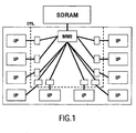
- As an example of such a shared-memory data processing system, a digital video platform (DVP) system in its basic form is shown in
Figure 1 . It comprises a plurality of data processing units IP which communicate via an off-chip memory SDRAM. The data processing units IP can be programmable devices like CPUs, application-specific hardware blocks, subsystems with a complex internal structure etc. Further provided in the system ofFigure 1 is a device transaction level (DTL) interface DTL via which each data processing unit IP is interfaced to a central main memory (MMI) interface MMI which arbitrates the accesses to the off-chip memory SDRAM. All IP-to-IP communication is done via logical buffers (not shown) mapped in the off-chip memory SDRAM. Usually, one of the data processing units IP is a CPU (central processing unit) which manages the configuration of a task graph by programming the data processing units via a network of memory mapped configuration registers (not shown). A synchronization among the data processing units IP is also handled in a centralized way by this CPU which notifies the data processing units IP via the memory mapped input/output network whether full or empty buffers are available. The data processing units IP notify the CPU via interrupt lines (not shown) whether these buffers have run empty or have been filled. - The mechanism used for synchronization results in that the buffers provided in the off-chip memory SDRAM must be rather large in order to keep the rate of the interrupts to the CPU low. For example, video processing units often synchronize at a coarse grain (e.g. a frame) even though from a functional perspective they could synchronize at a finer grain (e.g. a line).
- Since such a data processing system comprises a shared memory architecture, there is a single address space which is accessible to all data processing means. This simplifies the programming model. Further, the common memory means helps to provide cost-effective system solutions.
- However, such a data processing system in its basic form has a number of disadvantages which will become more eminent as technology progresses. Namely, as the number of data processing means increases, the number of connections to the memory interface increases resulting in a more complex memory interface. In particular, the arbitration among the different data processing means becomes more complex. Further, wire length may become a problem for the data processing means which are located far from the memory interface so that many long wires may cause wiring congestion as well as time delay and power consumption problems. A further critical disadvantage is that there is a potential bottleneck when bandwidth requirements increase further; the bandwidth to the (off-chip) memory means is restricted by certain aspects like signalling speed and pin count of the off-chip interconnect.
-
GB 2 233 480 A -
US 5,261,067 A discloses an apparatus and a method for ensuring data cache content integrity among parallel processors. Each processor has a data cache to store results of intermediate calculations. The data cache of each processor is synchronized with each other through the use of synchronization intervals. During entry of a synchronization interval, modified data variables contained in an individual cache are written back to a shared memory. The unmodified data contained in a data cache is flushed from the memory. During exiting of a synchronization interval, data variables which were not modified since entry into the synchronization interval are also flushed. By retaining modified data cache values in the individual processors which computed the modified values, unnecessary access to shared memory is avoided. -
US 6,253,290 B1 describes a multiprocessor system having a plurality of processor units each including a CPU and a local cache memory connected to the CPU. The CPUs have their shared bus terminals connected to a global shared bus, and local cache memories have their bus terminals connected to a global unshared bus. The global shared bus is connected to an external shared memory for storing shared information used in common by the CPUs, and the global unshared bus is connected to an external unshared memory for storing unshared information used by the CPUs. -
US 6,282,708 B1 discloses a method for structuring a multi-instruction computer program as containing a plurality of basic blocks which each compose from internal instructions and external instructions organized in an internal directed acyclic graph. A guarding is executed on successor instructions which each collectively emanate from a respectively associated single predecessor instruction. A subset of joined instructions which converge onto a single join/target instruction are then unconditionally joined. This is accomplished by letting each respective instruction in the subset of joined instructions be executed under mutually non-related conditions, specifying all operations with respect to a jump instruction, specifying all operations which must have been executed previously and linking various basic blocks comprising subsets of successor instructions in a directed acyclic graph which allows parallel execution of any further subset of instructions contained therein. -
US 5440698 discloses an arbiter provided for resolving contention on synchronous packet switched busses, including busses composed of a plurality of pipelined segments, to ensure that all devices serviced by such a bus are given fair, bounded time access to the bus and to permit such devices to fill all available bus cycles with packets. Flow control for shared memory multiprocessors is readily implemented with this arbiter because the arbiter supports different types of arbitration requests and the prioritization of such arbitration requests by type. - An object of the present invention is to overcome the above mentioned drawbacks and to improve the data processing system so as to avoid a communication bottleneck between the data processing and the memory means even when the bandwidth requirements increase further, to decrease the number of connections to the memory interface, and to reduce the wire length. The invention is defined by
claim 1. The dependent claims define advantageous embodiments. - Due to the construction according to the invention, the number of connections to the memory means is reduced. This is achieved by the provision of a specific physical organisation of a logically shared memory architecture wherein the communication interface means includes a network of a plurality of nodes having slave ports receiving memory access requests from the data processing means and at least one master port issuing a specific memory access request to the memory means. Typically, the number of master ports of a node is smaller than the number of slave ports of that node. As a result, the complexity of the memory interface is decreased since the number of clients connected thereto is reduced. Further, due to the interconnection of the communication interface means, the length of individual wires and, thus, the total length of wires are reduced so as to help avoiding wire congestion.
- The communication interface means includes a network of a plurality of nodes, wherein each node comprises at least one slave port for receiving a memory access request and at least one master port for issuing a memory access request in accordance with the memory access request received at said slave port(s), wherein the number of said slave ports can be higher than the number of said master ports. So, the communication interface means according to the present invention includes a node structure for the connections between the data processing means and the memory means wherein multiple data processing means can be connected to a node means via its slave ports, whereas each node has only one or a few master ports. Since the slave ports of a node are uniform in that they offer the same services, it is transparent to the node whether a slave port attaches a data processing means or another node. A request for a memory access issued by a data processing means is passed to one of the nodes to which it is connected. An advantage of the concept of the invention is that it can be introduced in a step-wise manner. Namely, a first chip to adopt the concept of the invention could use a new node for just a few data processing means; and in later chips, the number of nodes may gradually rise, and the facilities of the communication interface means of the invention may be used for more and more communication between data processing means. In case a node has multiple master ports, a single port is selected for forwarding, for example, in accordance with an address range discrimination.
- At least one local memory unit is attached to the communication interface, allowing such local memory unit to be selectively accessed to by a memory access request. So, a single address space is distributed over a global memory and such local memory unit(s). The advantage of this embodiment is that the data processing means may exchange data to each other via a local memory unit only instead of using the global memory, resulting in a further reduction of a potential bottleneck risk in the communication, by reducing memory access latency, reducing power consumption, and reducing the use of external memory bandwidth. At least one node further comprises at least one memory port to which a local memory unit is connected. The node may check whether or not the memory access request refers to the local memory unit(s) attached to such node by comparing the address of the memory access request with the address ranges associated to the local memory unit(s) attached to such node. If yes, the memory access is executed on the selected local memory unit. Otherwise, the node forwards the memory access request through one of its master ports either to a next node where the check and "access or forward" is repeated if a local memory unit is also attached to such next node, or to the memory means.
- In a first embodiment of the invention, each of the slave ports of said nodes is connected to one of said plurality of data processing means and the master ports of said nodes are coupled to said memory means. So, all the nodes are provided in the same level, and the data processing means are coupled to the memory means via such single level of nodes. The data processing means can issue memory access requests to an associated node which forwards the request to the memory means.
- In an alternative second embodiment, the network of nodes is hierarchically structured having the data processing means as leaves and the node means as nodes.
- The network of nodes can be arranged in a directed acyclic graph structure. Each edge of the directed acyclic graph structure corresponds to an interconnect path which serves memory access requests. The edges are directed, and each edge connects a master port of one node means to a slave port of another node means. In case the memory means includes a plurality of memory sections, the acyclic graph structure can result in a set of master ports each providing a connection to a different memory section, in such a way that each data processing means can communicate to one or more memory section(s), thereby allowing multiple data processing means to access different memory sections concurrently, thereby reducing the bandwidth bottleneck. Furthermore, the acyclic graph structure might provide several different paths through the graph leading from one data processing means to one memory section. These different paths can be employed advantageously to further reduce communication bottlenecks or to avoid the use of faulty connections.
- Further, in a preferred refinement of the above embodiment, the network of nodes may be arranged in a tree structure so that one or more data processing mean(s) and/or previous node(s) are connected to a node via its slave ports, but each node has only one master port. This simplifies the forwarding process in the node and provides connectivity to a single memory section at the root of the node tree that can be accessed by all data processing means.
- In this alternative second modification, preferably the network of nodes includes n groups of node means with n ≥ 2, wherein each of the slave ports of the nodes of a first group is connected to one of said plurality of data processing means, the master ports of the nodes of the nth group are coupled to said memory means, and each of the slave ports of the nodes of the nth group is connected to the master port of the nodes of the (n-1)th group. So, the network of nodes is divided into n groups, wherein each group defines a different level in the structure. If a node receives a memory access request at one of its slave ports, the request is forwarded to a node of a higher group or, if the node is in the highest (i.e. nth) group, to the memory means. With the respect thereto, it should be added that the node structure does not necessarily need to have a uniform depth. Some data processing means may be "close" to the memory means in that only one or two nodes separate them from the memory means, whereas (at the same time) other data processing means may be more "remote" from the memory means in that the memory access requests that they issue have to travel via a large number of nodes.
- The above mentioned hierarchical structure of the nodes is completely transparent to the data processing means so that no modifications of the data processing means are required.
- Preferably, the nodes are hubs.
- In a modification of the recently mentioned embodiment, the communication interface means includes a cache controller means for controlling the local memory unit(s) as a cache memory. In this case at least a part of the local memory unit is used to locally store a copy of data residing in other memories reachable via one of its master ports. So, memory access requests can be served locally for a wider address range for which caching behaviour is enabled.
- Moreover, the communication interface means may include at least one synchronization means for streaming communication between data processing means. In particular, at least one node includes said synchronization means for streaming communication between the data processing means directly or indirectly coupled to said node means.
- In case a local memory unit is attached to the node, the local memory unit should have a first-in/first-out (FIFO) function, and the synchronization means comprises a FIFO administration means for controlling said local memory unit(s). The synchronization services can be locally handled when the FIFO administration is locally stored, whereby multiple data processing means can communicate data via the local memory unit(s) attached to the node means; otherwise the synchronization request is forwarded to one of the master ports of the corresponding node.
- In a further preferred embodiment, the communication interface means is provided on a single chip. Moreover, at least a part of the plurality of data processing means may be additionally provided on said single chip.
- The above described objects and other aspects of the present invention will be better understood by the following description and the accompanying figures.
- Preferred embodiments of the present invention are described with reference to the drawings in which
-
Fig. 1 shows a schematic basic block diagram of a DVP system in its basic form according to the prior art; -
Fig. 2 shows a schematic basic block diagram of a DVP system including a hub structure according to a first preferred embodiment of the present invention; -
Fig. 3 shows a schematic basic block diagram of a DVP system with a hub structure according to a second preferred embodiment of the present invention which further includes on-chip local memories; and -
Fig. 4 shows a schematic basic block diagram of a DVP system including a hub structure according to a third preferred embodiment of the present invention. -
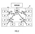
Figure 2 shows a digital video platform (DVP) system having a hub structure according to a first preferred embodiment of the present invention. Like the system shown inFigure 1 , the system ofFigure 2 comprises a plurality of data processing units IP, which may also be called intellectual property (IP) units, and a memory SDRAM. The data processing units IP can be programmable devices (CPUs), application-specific hardware blocks, subsystems with a complex internal structure etc. All data processing units comprise a device transaction level (DTL) interface. Further, there are provided a plurality of hubs H11, H12, H2, wherein each hub comprises several slave ports s and one master port m. In the system ofFigure 2 , the hubs define a network of hubs comprising a first group of hubs H11 and H12 and a second group consisting of only one hub H2. The first group of hubs H11 and H12 define a first level adjacent to the data processing units IP so that the hubs H11 and H12 of the first group are directly connected to the data processing units IP via its slave ports s. In the embodiment ofFigure 2 , each hub has only one master port m for connection to the next hub or the memory interface MMI. The hubs H11 of the first group are connected via its master ports m to the slave ports s of the hub H2 of the second group which is connected via its master port m to the memory interface MMI whereas the hubs H12 of the first group are directly connected via its master ports m to the memory interface MMI. The memory interface MMI is coupled to the memory SDRAM. - In the embodiment of
Figure 2 , the network of hubs is organized as a directed acyclic graph (DAG) structure wherein the nodes of the DAG structure are defined by the hubs H11, H12 and H2, and each edge of the DAG structure corresponds to an interconnect path which serves memory access requests. The edges are directed. The DAG structure shown inFigure 2 is restricted to have a tree structure wherein each hub H12, H11 and H2 has one master port only. This simplifies the forwarding process in the hubs, as they do not need to select a master port for each memory request, for example by discriminating ranges on the requested address. - At the slave ports s of the hubs a memory access request is received which is forwarded by the master port m. The slave ports s of a hub are uniform in that they offer the same services. Therefore, it is transparent to the hub whether a slave port s is connected to a data processing unit IP or another hub.
- It is noted that many modifications of the structure over the embodiment of
Figure 2 are possible and thatFigure 2 gives only one example. So, the network of hubs may include more than two levels. Further, the hubs H12 may be connected to a next hub higher in the structure. Moreover, a hub may have multiple master ports wherein a single master port is selected for forwarding, for example in accordance with an address range discrimination. - As further shown in
Figure 2 , the data processing units, the device transaction level DTL, the hubs H11, H12 and H2 and the memory interface MMI reside on a single chip C, whereas the memory SDRAM is provided outside the chip C. - Due to the hub structure shown in
Figure 2 , the number of clients of the memory interface MMI is reduced. Further, the length of individual wires and, thus, the total length of wires are reduced whereby wire congestion is avoided. - The hierarchical hub structure is completely transparent to the data processing units IP, and no modifications of the data processing units IP are required. Also it does not affect the way synchronization is performed; this may still be handled in a centralized way by means of a memory mapped input/output (not shown) and interrupts via a data processing unit including a CPU.
-
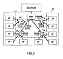
Figure 3 shows a second preferred embodiment of the present invention which differs from the first embodiment ofFigure 2 in that an embedded local memory MEM is attached to each of the hubs. However, with respect thereto it should be noted that in an alternative embodiment local memories are provided for only some of the hubs. The local memories MEM are assigned private segments in the address space; wherein a single address space is provided which is distributed over the off-chip memory SDRAM and the multiple local memories MEM. The data processing units IP perform memory access requests in the usual address-based way, wherein an address can refer to the off-chip memory SDRAM or to an on-chip local memory MEM. All data processing units IP are able to access the off-chip memory SDRAM and a further on-chip local memory MEM attached to the memory interface MMI, but not all data processing units IP are able to access all on-chip local memories MEM attached to the hubs H11, H12 and H2. Namely, the data processing units IP can access only the local memories MEM attached to the hubs on the route to the memory interface MMI. - For the data processing units IP sharing a common hub, a buffered communication can be performed via the local memory MEM attached to that hub. A first-in/first-out (FIFO) buffer used for a communication between the data processing units is mapped to a memory segment of the local memory MEM attached to a common hub, preferably to the common hub H11 or H12 of the first group being the closest common hub. The data processing units IP are simply instructed to access the data in the address range in which such buffer has been allocated via their DTL interface, but are unaware of the physical location; this is transparent to the data processing units IP. The hubs check the addresses of the memory access requests performed by the data processing units IP and either perform an access to their local memory MEM, if the address is in the specified range, or forward the request up in the hierarchy. The buffers for the IP-to-IP communication can be allocated to the local memories MEM upon configuration, wherein the address range of the buffer is programmed in the hub to which the local memory MEM is attached.
- The IP-to-IP communication which is mapped to a communication via an on-chip local memory MEM does not consume expensive bandwidth to the off-chip memory SDRAM. The hub structure should be chosen such that the data processing units IP which need to communicate frequently have a common hub for a communication via the local memory attached to such common hub. For example, video data processing units IP should be in the same sub-tree of the hub structure. Moreover, the total available memory bandwidth is increased significantly. In parallel to accesses to the off-chip memory SDRAM by some data processing units IP, accesses to the on-chip local memories may be performed by data processing units IP located in other (disjunct) sub-trees. Further, the communication via the on-chip local memories MEM is more power efficient and can more easily support higher bandwidth (wider interconnects and memory ports, higher clocks).
- As explained above, the data processing units IP can simply access data via their DTL interface, irrespective of whether or not that data is located on-chip (local memory MEM) or off-chip (memory SDRAM). Hence, on-chip communication is transparent to the data processing units IP. This facilitates re-use of the data processing units IP in the proposed configuration.
- Special attention should be paid to the synchronization among the data processing units IP. As already mentioned above, in the DVP system synchronization is performed by a data processing unit including a CPU, requiring low rate synchronization at a coarse data grain. This results in larger buffer sizes which can easily be accommodated in the off-chip SDRAM. For on-chip communication, however, smaller buffers should be used, which requires synchronization at a finer data grain. For the functions performed by many data processing units, synchronization at a finer grain (e.g. line or macro block) is merely logical. However, using an interrupt-based scheme for synchronization at a finer grain would lead to a higher interrupt rate on the CPU.
- One solution may be to dedicate more CPU power to synchronization or even to dedicate a special (light-weight) CPU to the synchronization task.
- Another attractive solution is to add synchronization support to the hubs. In this case, each hub can perform the synchronization tasks which are related to the (FIFO-based) IP-to-IP communication via the local memory MEM attached to such hub; i.e., per first-in/first-out operation the availability of data and room is administered and signalled to the data processing units IP. As an effect, this supports continuous (autonomous) operation of the data processing units without CPU software intervention, at least as far as communication via local memories is involved.
- It is proposed that the data processing units IP need to make abstract synchronization calls at their ports. The infrastructure decides how these synchronization calls are resolved, dependent on how the data processing unit IP is integrated in a system-on-chip. This would not be hardwired in a re-usable data processing unit. For example, if such a port maps to local communication via a local memory, the corresponding hub resolves the synchronization call locally or forwards it to the next higher hub. If the communication is done via the off-chip memory SDRAM, an interrupt may be generated. For the data processing unit IP this is hidden by an "abstract" interface (not shown) which is configured such that it offers a function to the data processing units IP to issue high level requests to the communication interface, but hides from the data processing units how such requests are implemented. When a buffer is provided in the local memory MEM attached to a hub, the port addresses for the synchronization are programmed in the hub together with the address range of the buffer at the configuration time, accordingly.
- It is noted that in the scheme presented above the local memories MEM are used for buffered IP-to-IP communication in which no data needs to travel to the off-chip SDRAM at all. This is different from the use of the on-chip local memories as a cache for copying data from the off-chip SDRAM into an on-chip local memory MEM for repeated use.
- However, the architecture of
Figure 3 could be used to support caching as well, wherein two kinds of caching are distinguished: Transparent caching and IP controlled caching. - With transparent caching, the data processing units IP are not really aware of that data are copied to a local memory MEM, other than that it perceives a different latency in accessing the data. By means of a cache control function, data are copied from/to the off-chip memory SDRAM to/from an on-chip local memory MEM. Such cache control is implemented in a hub. Cache coherency must be resolved either by implementing a hardware cache coherency scheme or by adopting restrictions in the programming model.
- With IP-controlled caching, a data processing unit IP itself copies data from the off-chip memory SDRAM to an on-chip local memory for repeated (fine-grain) use. The copies in the on-chip local memory MEM are in a different address range than the corresponding data in the off-chip memory SDRAM. With IP-controlled caching, the data processing units IP are responsible for the coherency. As an example of IP-controlled caching, it may be considered a three-dimensional graphics renderer which 'caches' texture data in an on-chip local memory MEM to perform fine grain accesses on it. This is done by copying the texture data to the address range of the local memory MEM attached to a hub and referring to addresses in that address range when performing the fine grain accesses. In such case, the cache control is performed by the data processing units IP themselves, and this kind of use is different from the transparent use of the on-chip local memory for IP-to-IP communication. Nevertheless, the architecture of
Figure 3 supports this kind of use. -
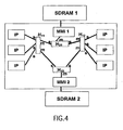
Figure 4 shows a third preferred embodiment which differs from the first embodiment offigure 2 in that in addition to a first off-chip memory SDRAM 1 and an associated firstmemory interface MMI 1 coupled thereto a second off-chip memory SDRAM 2 and an associated secondmemory interface MMI 2 coupled thereto are provided. Further, there are provided a plurality of hubs H11, H12, H21 and H22, wherein the hubs H11 and H12 each comprises several slave ports s and two master ports m and the hubs H21 and H22 each comprises two slave ports s and one master port m. So, in the system offigure 4 , the hubs define a network of hubs comprising a first group of hubs H1 and H12 and a second group consisting of hubs H21 and H22. The first group of hubs H11 and H12 define a first level adjacent to the data processing units IP so that the hubs H11 and H12 of the first group are directly connected to the data processing units IP via its slave ports s. The second group of hubs H21 and H22 define a second level adjacent to thememory interfaces MMI 1 andMMI 2, wherein the hubs H21 and H22 each are connected via one of its slave ports to one of the master ports m of the hub H11 and further via the other one of its slave ports s to one of the master ports m of the hub H12. Moreover, the hub H21 is connected via its master port m to the firstmemory interface MMI 1, and the hub H22 is connected via its master port m to the secondmemory interface MMI 2. - So, in the third embodiment of
figure 4 , the network of hubs is organized as a DAG structure like in the first and second embodiments offigures 2 and3 , respectively, but the data processing units IP have optional access to two offchip memories SDRAM 1 andSDRAM 2, whereas in the first and second embodiments offigures 2 and3 there is only communication between a single off chip memory SDRAM and the data processing units IP. Apart from that two off-chip memories SDRAM 1 andSDRAM 2 are connected to the network of hubs, the operation of the third embodiment offigure 4 is the same as that of the first embodiment offigure 2 so that reference is made to the description offigure 2 . Further, in the third embodiment offigure 4 local memories and a synchronisation as described in conjunction withfigure 3 may optionally be provided as well. - As described above, the third embodiment of
figure 4 comprises two off-chip memories SDRAM 1 andSDRAM 2. However, more than two off-chip memories may be provided as well. - In the above description, it has been presented a next step in the evolution of a multi-processing data system like a DVP platform which allows the use of on-chip local memories MEM to avoid a communication bottleneck to the off-chip memory SDRAM. The use of the local memories MEM for IP-to-IP communication is largely transparent to the data processing units IP.
- A further advantage of the above described architecture according to the present invention is-that it can be introduced in a stepwise manner. A first chip to adopt the solution can use an on-chip local memory MEM and a new hub (e.g. H12) for just a few data processing units IP which want to communicate via such local memory MEM. In later chips, the number of hubs with local memories may gradually rise, and the on-chip communication facilities may be used for more and more IP-to-IP communication.
- Although the invention is described above with reference to examples shown in the attached drawings, it is apparent that the invention is not restricted to it but can vary in many ways within the scope disclosed in the attached claims.
Claims (13)
- A data processing system, comprising:a memory means (SDRAM),a plurality of data processing means (IP) provided for accessing to said memory means (SDRAM), anda communication interface means coupled between said memory means (SDRAM) and said plurality of data processing means (IP), said communication interface means including:- a network of nodes (H11, H12, H2), each node comprising at least one slave port (s) for receiving a memory access request from a respective one of said plurality of data processing means (IP) or from a previous node, and at least one master port (m) for issueing a memory access request to a next node or to said memory means (SDRAM) in accordance with the memory access request received at said slave port (s), wherein said at least one slave port (s) is connected to a master port (m) of a previous node or to said respective one of said plurality of data processing means (IP), and said at least one master port (m) is connected to a slave port (s) of a next node or to said memory means (SDRAM); and- at least one local memory unit (MEM) adapted to be selectively accessed to by a memory access request, the data processing system being characterized in that a single address space is distributed over the memory (SDRAM) and the at least one local memory unit (MEM), at least some nodes (H11, H12, H2) further comprising at least one memory port (mp) to which a respective local memory unit (MEM) is connected, enabling the local memories (MEM) to be used for buffered communication between different ones of said plurality of data processing means (IP) in which buffered communication no data needs to travel to the memory means (SDRAM).
- The data processing system according to claim 1, characterized in that at each node the number of said slave ports (s) is higher than the number of said master ports (m).
- The data processing system according to claim 1 or 2, characterized in that said network of nodes (H11, H12, H2) is hierarchically structured.
- The data processing system according to claim 3, characterized in that said network of nodes (H11, H12, H2) is arranged in a directed acyclic graph structure.
- The data processing system according to claim 4, characterized in that said network of nodes (H11, H12, H2) is arranged in a tree structure.
- The data processing system according to at least any one of the preceding claims, characterized in that said network of nodes (H11, H12, H2) includes n groups of nodes with n ≥ 2, wherein each of the slave ports (s) of the nodes (H11) of a first group is connected to one of said plurality of data processing means (IP), the master ports (m) of the nodes (H2) of the nth group are coupled to said memory means (SDRAM), and each of the slave ports (s) of the nodes (H2) of the nth group is connected to a master port (m) of the nodes (H11) of the (n-1)th group.
- The data processing system according to at least any one of the preceding claims, characterized in that said nodes (H11, H12, H2) are hubs.
- The data processing system according to claim 1, characterized in that said communication interface means includes a cache controller means for controlling at least a section of the local memory unit(s) (MEM) as a cache memory.
- The data processing system according to at least any one of the preceding claims, characterized in that said communication interface means further includes at least one synchronization means for streaming communication between data processing means (IP).
- The data processing system according to claim 9, characterized in that at least one node (H11, H12, H2) includes said synchronization means for streaming communication between the data processing means (IP) directly or indirectly coupled to said node means.
- The data processing system according to claim 1 as well as to claim 9 or 10, characterized in that the local memory unit(s) (MEM) is (are) configured to provide the storage means for a first-in/first-out function and said synchronization means comprises a first-in/first-out administration means for controlling said local memory unit(s) (MEM).
- The data processing system according to at least any one of the preceding claims, characterized in that said communication interface means is provided on a single chip (C).
- The data processing system according to claim 12, characterized in that at least a part of said plurality of data processing means (IP) is additionally provided on said single chip (C).
Priority Applications (1)
| Application Number | Priority Date | Filing Date | Title |
|---|---|---|---|
| EP04769826A EP1671233B1 (en) | 2003-09-04 | 2004-08-19 | Tree-like data processing system accessing a memory |
Applications Claiming Priority (3)
| Application Number | Priority Date | Filing Date | Title |
|---|---|---|---|
| EP03103293 | 2003-09-04 | ||
| EP04769826A EP1671233B1 (en) | 2003-09-04 | 2004-08-19 | Tree-like data processing system accessing a memory |
| PCT/IB2004/051491 WO2005026964A2 (en) | 2003-09-04 | 2004-08-19 | Data processing system |
Publications (2)
| Publication Number | Publication Date |
|---|---|
| EP1671233A2 EP1671233A2 (en) | 2006-06-21 |
| EP1671233B1 true EP1671233B1 (en) | 2011-11-16 |
Family
ID=34306924
Family Applications (1)
| Application Number | Title | Priority Date | Filing Date |
|---|---|---|---|
| EP04769826A Active EP1671233B1 (en) | 2003-09-04 | 2004-08-19 | Tree-like data processing system accessing a memory |
Country Status (7)
| Country | Link |
|---|---|
| US (1) | US7870347B2 (en) |
| EP (1) | EP1671233B1 (en) |
| JP (1) | JP4729490B2 (en) |
| KR (1) | KR101109016B1 (en) |
| CN (1) | CN100520748C (en) |
| AT (1) | ATE534080T1 (en) |
| WO (1) | WO2005026964A2 (en) |
Families Citing this family (10)
| Publication number | Priority date | Publication date | Assignee | Title |
|---|---|---|---|---|
| CN100445977C (en) * | 2004-05-18 | 2008-12-24 | 皇家飞利浦电子股份有限公司 | Integrated circuit and method for buffering to optimize burst length in networks on chips |
| US7561584B1 (en) * | 2005-11-09 | 2009-07-14 | Sun Microsystems, Inc. | Implementation of a graph property in a switching fabric for fast networking |
| CN103186501A (en) * | 2011-12-29 | 2013-07-03 | 中兴通讯股份有限公司 | Multiprocessor shared storage method and system |
| RU2678321C2 (en) | 2013-09-02 | 2019-01-28 | Филипс Лайтинг Холдинг Б.В. | Transparent computer structure |
| US20160164999A1 (en) * | 2014-12-09 | 2016-06-09 | International Business Machines Corporation | Hybrid web storage model |
| CN107368523B (en) * | 2017-06-07 | 2020-05-12 | 武汉斗鱼网络科技有限公司 | Data processing method and system |
| KR102109371B1 (en) | 2018-01-15 | 2020-05-12 | 주식회사 경인기계 | Fan and cooling tower comprising the same |
| WO2020001438A1 (en) * | 2018-06-27 | 2020-01-02 | 上海寒武纪信息科技有限公司 | On-chip code breakpoint debugging method, on-chip processor, and chip breakpoint debugging system |
| WO2020078470A1 (en) * | 2018-10-18 | 2020-04-23 | 上海寒武纪信息科技有限公司 | Network-on-chip data processing method and device |
| US11250015B2 (en) | 2020-02-07 | 2022-02-15 | Coupang Corp. | Systems and methods for low-latency aggregated-data provision |
Family Cites Families (13)
| Publication number | Priority date | Publication date | Assignee | Title |
|---|---|---|---|---|
| JPS63236159A (en) * | 1987-03-25 | 1988-10-03 | Hitachi Ltd | Memory access system for parallel processor |
| GB8713460D0 (en) * | 1987-06-09 | 1987-07-15 | Philips Nv | Data processing system |
| GB8914352D0 (en) * | 1989-06-22 | 1989-08-09 | Int Computers Ltd | Multiprocessor data processing system |
| US5261067A (en) | 1990-04-17 | 1993-11-09 | North American Philips Corp. | Method and apparatus for providing synchronized data cache operation for processors in a parallel processing system |
| CA2051029C (en) * | 1990-11-30 | 1996-11-05 | Pradeep S. Sindhu | Arbitration of packet switched busses, including busses for shared memory multiprocessors |
| US5469542A (en) * | 1991-07-22 | 1995-11-21 | International Business Machines Corporation | Serial diagnostic interface bus for multiprocessor systems |
| JP2819982B2 (en) * | 1993-03-18 | 1998-11-05 | 株式会社日立製作所 | Multiprocessor system with cache match guarantee function that can specify range |
| US6292705B1 (en) | 1998-09-29 | 2001-09-18 | Conexant Systems, Inc. | Method and apparatus for address transfers, system serialization, and centralized cache and transaction control, in a symetric multiprocessor system |
| TW440793B (en) | 1998-02-25 | 2001-06-16 | Koninkl Philips Electronics Nv | A method for structuring a multi-instruction computer program from basic blocks that compose from internal instructions and external jumps in an internal directed acyclic graph, and a processor loaded with such program |
| JP4179677B2 (en) | 1998-09-04 | 2008-11-12 | 株式会社ルネサステクノロジ | Multiprocessor device |
| US6625700B2 (en) * | 2001-05-31 | 2003-09-23 | Sun Microsystems, Inc. | Arbitration and select logic for accessing a shared memory |
| US6961804B2 (en) * | 2001-07-20 | 2005-11-01 | International Business Machines Corporation | Flexible techniques for associating cache memories with processors and main memory |
| US7024506B1 (en) * | 2002-12-27 | 2006-04-04 | Cypress Semiconductor Corp. | Hierarchically expandable fair arbiter |
-
2004
- 2004-08-19 US US10/570,236 patent/US7870347B2/en active Active
- 2004-08-19 KR KR1020067004411A patent/KR101109016B1/en not_active IP Right Cessation
- 2004-08-19 CN CNB2004800252825A patent/CN100520748C/en active Active
- 2004-08-19 AT AT04769826T patent/ATE534080T1/en active
- 2004-08-19 EP EP04769826A patent/EP1671233B1/en active Active
- 2004-08-19 WO PCT/IB2004/051491 patent/WO2005026964A2/en active Application Filing
- 2004-08-19 JP JP2006525227A patent/JP4729490B2/en not_active Expired - Fee Related
Also Published As
| Publication number | Publication date |
|---|---|
| EP1671233A2 (en) | 2006-06-21 |
| KR20060080186A (en) | 2006-07-07 |
| WO2005026964A2 (en) | 2005-03-24 |
| JP4729490B2 (en) | 2011-07-20 |
| US7870347B2 (en) | 2011-01-11 |
| KR101109016B1 (en) | 2012-01-31 |
| CN100520748C (en) | 2009-07-29 |
| US20070028038A1 (en) | 2007-02-01 |
| CN1902611A (en) | 2007-01-24 |
| JP2007504549A (en) | 2007-03-01 |
| WO2005026964A3 (en) | 2006-08-31 |
| ATE534080T1 (en) | 2011-12-15 |
Similar Documents
| Publication | Publication Date | Title |
|---|---|---|
| CN108027804B (en) | On-chip atomic transaction engine | |
| US6496740B1 (en) | Transfer controller with hub and ports architecture | |
| US20160299714A1 (en) | Computing architecture with peripherals | |
| JP2512651B2 (en) | Memory sharing multiprocessor | |
| US8473667B2 (en) | Network on chip that maintains cache coherency with invalidation messages | |
| US8407432B2 (en) | Cache coherency sequencing implementation and adaptive LLC access priority control for CMP | |
| US10169087B2 (en) | Technique for preserving memory affinity in a non-uniform memory access data processing system | |
| CN102375800A (en) | Multiprocessor system-on-a-chip for machine vision algorithms | |
| JPH1097513A (en) | Node in multiprocessor computer system and multiprocessor computer system | |
| WO2001024031A9 (en) | Multiprocessor node controller circuit and method | |
| TWI573076B (en) | Communication of message signalled interrupts | |
| EP1671233B1 (en) | Tree-like data processing system accessing a memory | |
| US10810146B2 (en) | Regulation for atomic data access requests | |
| WO1999034294A1 (en) | Optimal multi-channel memory controller system | |
| Jang et al. | An SDRAM-aware router for networks-on-chip | |
| US6038642A (en) | Method and system for assigning cache memory utilization within a symmetric multiprocessor data-processing system | |
| US6681270B1 (en) | Effective channel priority processing for transfer controller with hub and ports | |
| KR20220160489A (en) | Cache for storing coherent and non-coherent data | |
| US10740032B2 (en) | Resource allocation for atomic data access requests | |
| US20030229721A1 (en) | Address virtualization of a multi-partitionable machine | |
| JP2005508549A (en) | Improved bandwidth for uncached devices | |
| JP2002198987A (en) | Active port of transfer controller with hub and port | |
| JP2015170313A (en) | Arithmetic processing unit and control method of arithmetic processing unit | |
| NZ716954B2 (en) | Computing architecture with peripherals | |
| JP2000148697A (en) | Computer system |
Legal Events
| Date | Code | Title | Description |
|---|---|---|---|
| PUAI | Public reference made under article 153(3) epc to a published international application that has entered the european phase |
Free format text: ORIGINAL CODE: 0009012 |
|
| AK | Designated contracting states |
Kind code of ref document: A2 Designated state(s): AT BE BG CH CY CZ DE DK EE ES FI FR GB GR HU IE IT LI LU MC NL PL PT RO SE SI SK TR |
|
| AX | Request for extension of the european patent |
Extension state: AL HR LT LV MK |
|
| PUAK | Availability of information related to the publication of the international search report |
Free format text: ORIGINAL CODE: 0009015 |
|
| RIC1 | Information provided on ipc code assigned before grant |
Ipc: G06F 13/16 20060101AFI20060928BHEP |
|
| DAX | Request for extension of the european patent (deleted) | ||
| 17P | Request for examination filed |
Effective date: 20070228 |
|
| RBV | Designated contracting states (corrected) |
Designated state(s): AT BE BG CH CY CZ DE DK EE ES FI FR GB GR HU IE IT LI LU MC NL PL PT RO SE SI SK TR |
|
| 17Q | First examination report despatched |
Effective date: 20091208 |
|
| RTI1 | Title (correction) |
Free format text: TREE-LIKE DATA PROCESSING SYSTEM ACCESSING A MEMORY |
|
| GRAP | Despatch of communication of intention to grant a patent |
Free format text: ORIGINAL CODE: EPIDOSNIGR1 |
|
| GRAS | Grant fee paid |
Free format text: ORIGINAL CODE: EPIDOSNIGR3 |
|
| GRAA | (expected) grant |
Free format text: ORIGINAL CODE: 0009210 |
|
| AK | Designated contracting states |
Kind code of ref document: B1 Designated state(s): AT BE BG CH CY CZ DE DK EE ES FI FR GB GR HU IE IT LI LU MC NL PL PT RO SE SI SK TR |
|
| REG | Reference to a national code |
Ref country code: GB Ref legal event code: FG4D |
|
| REG | Reference to a national code |
Ref country code: CH Ref legal event code: EP |
|
| REG | Reference to a national code |
Ref country code: IE Ref legal event code: FG4D |
|
| REG | Reference to a national code |
Ref country code: DE Ref legal event code: R096 Ref document number: 602004035339 Country of ref document: DE Effective date: 20120112 |
|
| REG | Reference to a national code |
Ref country code: NL Ref legal event code: VDEP Effective date: 20111116 |
|
| PG25 | Lapsed in a contracting state [announced via postgrant information from national office to epo] |
Ref country code: GR Free format text: LAPSE BECAUSE OF FAILURE TO SUBMIT A TRANSLATION OF THE DESCRIPTION OR TO PAY THE FEE WITHIN THE PRESCRIBED TIME-LIMIT Effective date: 20120217 Ref country code: SE Free format text: LAPSE BECAUSE OF FAILURE TO SUBMIT A TRANSLATION OF THE DESCRIPTION OR TO PAY THE FEE WITHIN THE PRESCRIBED TIME-LIMIT Effective date: 20111116 Ref country code: NL Free format text: LAPSE BECAUSE OF FAILURE TO SUBMIT A TRANSLATION OF THE DESCRIPTION OR TO PAY THE FEE WITHIN THE PRESCRIBED TIME-LIMIT Effective date: 20111116 Ref country code: PT Free format text: LAPSE BECAUSE OF FAILURE TO SUBMIT A TRANSLATION OF THE DESCRIPTION OR TO PAY THE FEE WITHIN THE PRESCRIBED TIME-LIMIT Effective date: 20120316 Ref country code: BE Free format text: LAPSE BECAUSE OF FAILURE TO SUBMIT A TRANSLATION OF THE DESCRIPTION OR TO PAY THE FEE WITHIN THE PRESCRIBED TIME-LIMIT Effective date: 20111116 Ref country code: SI Free format text: LAPSE BECAUSE OF FAILURE TO SUBMIT A TRANSLATION OF THE DESCRIPTION OR TO PAY THE FEE WITHIN THE PRESCRIBED TIME-LIMIT Effective date: 20111116 Ref country code: PL Free format text: LAPSE BECAUSE OF FAILURE TO SUBMIT A TRANSLATION OF THE DESCRIPTION OR TO PAY THE FEE WITHIN THE PRESCRIBED TIME-LIMIT Effective date: 20111116 |
|
| PG25 | Lapsed in a contracting state [announced via postgrant information from national office to epo] |
Ref country code: CY Free format text: LAPSE BECAUSE OF FAILURE TO SUBMIT A TRANSLATION OF THE DESCRIPTION OR TO PAY THE FEE WITHIN THE PRESCRIBED TIME-LIMIT Effective date: 20111116 |
|
| PG25 | Lapsed in a contracting state [announced via postgrant information from national office to epo] |
Ref country code: BG Free format text: LAPSE BECAUSE OF FAILURE TO SUBMIT A TRANSLATION OF THE DESCRIPTION OR TO PAY THE FEE WITHIN THE PRESCRIBED TIME-LIMIT Effective date: 20120216 Ref country code: SK Free format text: LAPSE BECAUSE OF FAILURE TO SUBMIT A TRANSLATION OF THE DESCRIPTION OR TO PAY THE FEE WITHIN THE PRESCRIBED TIME-LIMIT Effective date: 20111116 Ref country code: DK Free format text: LAPSE BECAUSE OF FAILURE TO SUBMIT A TRANSLATION OF THE DESCRIPTION OR TO PAY THE FEE WITHIN THE PRESCRIBED TIME-LIMIT Effective date: 20111116 Ref country code: CZ Free format text: LAPSE BECAUSE OF FAILURE TO SUBMIT A TRANSLATION OF THE DESCRIPTION OR TO PAY THE FEE WITHIN THE PRESCRIBED TIME-LIMIT Effective date: 20111116 Ref country code: EE Free format text: LAPSE BECAUSE OF FAILURE TO SUBMIT A TRANSLATION OF THE DESCRIPTION OR TO PAY THE FEE WITHIN THE PRESCRIBED TIME-LIMIT Effective date: 20111116 |
|
| PG25 | Lapsed in a contracting state [announced via postgrant information from national office to epo] |
Ref country code: RO Free format text: LAPSE BECAUSE OF FAILURE TO SUBMIT A TRANSLATION OF THE DESCRIPTION OR TO PAY THE FEE WITHIN THE PRESCRIBED TIME-LIMIT Effective date: 20111116 Ref country code: IT Free format text: LAPSE BECAUSE OF FAILURE TO SUBMIT A TRANSLATION OF THE DESCRIPTION OR TO PAY THE FEE WITHIN THE PRESCRIBED TIME-LIMIT Effective date: 20111116 |
|
| REG | Reference to a national code |
Ref country code: AT Ref legal event code: MK05 Ref document number: 534080 Country of ref document: AT Kind code of ref document: T Effective date: 20111116 |
|
| PLBE | No opposition filed within time limit |
Free format text: ORIGINAL CODE: 0009261 |
|
| STAA | Information on the status of an ep patent application or granted ep patent |
Free format text: STATUS: NO OPPOSITION FILED WITHIN TIME LIMIT |
|
| 26N | No opposition filed |
Effective date: 20120817 |
|
| PGFP | Annual fee paid to national office [announced via postgrant information from national office to epo] |
Ref country code: GB Payment date: 20120831 Year of fee payment: 9 |
|
| REG | Reference to a national code |
Ref country code: DE Ref legal event code: R097 Ref document number: 602004035339 Country of ref document: DE Effective date: 20120817 |
|
| PG25 | Lapsed in a contracting state [announced via postgrant information from national office to epo] |
Ref country code: AT Free format text: LAPSE BECAUSE OF FAILURE TO SUBMIT A TRANSLATION OF THE DESCRIPTION OR TO PAY THE FEE WITHIN THE PRESCRIBED TIME-LIMIT Effective date: 20111116 |
|
| REG | Reference to a national code |
Ref country code: CH Ref legal event code: PL |
|
| PG25 | Lapsed in a contracting state [announced via postgrant information from national office to epo] |
Ref country code: MC Free format text: LAPSE BECAUSE OF NON-PAYMENT OF DUE FEES Effective date: 20120831 |
|
| PG25 | Lapsed in a contracting state [announced via postgrant information from national office to epo] |
Ref country code: CH Free format text: LAPSE BECAUSE OF NON-PAYMENT OF DUE FEES Effective date: 20120831 Ref country code: LI Free format text: LAPSE BECAUSE OF NON-PAYMENT OF DUE FEES Effective date: 20120831 Ref country code: ES Free format text: LAPSE BECAUSE OF FAILURE TO SUBMIT A TRANSLATION OF THE DESCRIPTION OR TO PAY THE FEE WITHIN THE PRESCRIBED TIME-LIMIT Effective date: 20120227 |
|
| REG | Reference to a national code |
Ref country code: IE Ref legal event code: MM4A |
|
| PG25 | Lapsed in a contracting state [announced via postgrant information from national office to epo] |
Ref country code: FI Free format text: LAPSE BECAUSE OF FAILURE TO SUBMIT A TRANSLATION OF THE DESCRIPTION OR TO PAY THE FEE WITHIN THE PRESCRIBED TIME-LIMIT Effective date: 20111116 |
|
| PG25 | Lapsed in a contracting state [announced via postgrant information from national office to epo] |
Ref country code: IE Free format text: LAPSE BECAUSE OF NON-PAYMENT OF DUE FEES Effective date: 20120819 Ref country code: DE Free format text: LAPSE BECAUSE OF NON-PAYMENT OF DUE FEES Effective date: 20130301 |
|
| REG | Reference to a national code |
Ref country code: DE Ref legal event code: R119 Ref document number: 602004035339 Country of ref document: DE Effective date: 20130301 |
|
| GBPC | Gb: european patent ceased through non-payment of renewal fee |
Effective date: 20130819 |
|
| PG25 | Lapsed in a contracting state [announced via postgrant information from national office to epo] |
Ref country code: TR Free format text: LAPSE BECAUSE OF FAILURE TO SUBMIT A TRANSLATION OF THE DESCRIPTION OR TO PAY THE FEE WITHIN THE PRESCRIBED TIME-LIMIT Effective date: 20111116 |
|
| PG25 | Lapsed in a contracting state [announced via postgrant information from national office to epo] |
Ref country code: LU Free format text: LAPSE BECAUSE OF NON-PAYMENT OF DUE FEES Effective date: 20120819 |
|
| PG25 | Lapsed in a contracting state [announced via postgrant information from national office to epo] |
Ref country code: GB Free format text: LAPSE BECAUSE OF NON-PAYMENT OF DUE FEES Effective date: 20130819 Ref country code: HU Free format text: LAPSE BECAUSE OF FAILURE TO SUBMIT A TRANSLATION OF THE DESCRIPTION OR TO PAY THE FEE WITHIN THE PRESCRIBED TIME-LIMIT Effective date: 20040819 |
|
| REG | Reference to a national code |
Ref country code: FR Ref legal event code: CA Effective date: 20141126 Ref country code: FR Ref legal event code: CD Owner name: KONINKLIJKE PHILIPS ELECTRONICS N.V., NL Effective date: 20141126 |
|
| REG | Reference to a national code |
Ref country code: FR Ref legal event code: PLFP Year of fee payment: 13 |
|
| REG | Reference to a national code |
Ref country code: FR Ref legal event code: PLFP Year of fee payment: 14 |
|
| REG | Reference to a national code |
Ref country code: FR Ref legal event code: PLFP Year of fee payment: 15 |
|
| PGFP | Annual fee paid to national office [announced via postgrant information from national office to epo] |
Ref country code: FR Payment date: 20220822 Year of fee payment: 19 |