EP1669780A1 - Optical element, method of manufacturing same, and optical apparatus using optical element - Google Patents
Optical element, method of manufacturing same, and optical apparatus using optical element Download PDFInfo
- Publication number
- EP1669780A1 EP1669780A1 EP05257609A EP05257609A EP1669780A1 EP 1669780 A1 EP1669780 A1 EP 1669780A1 EP 05257609 A EP05257609 A EP 05257609A EP 05257609 A EP05257609 A EP 05257609A EP 1669780 A1 EP1669780 A1 EP 1669780A1
- Authority
- EP
- European Patent Office
- Prior art keywords
- optical element
- layer
- periodic
- grating
- element according
- Prior art date
- Legal status (The legal status is an assumption and is not a legal conclusion. Google has not performed a legal analysis and makes no representation as to the accuracy of the status listed.)
- Withdrawn
Links
Images


Classifications
-
- G—PHYSICS
- G02—OPTICS
- G02B—OPTICAL ELEMENTS, SYSTEMS OR APPARATUS
- G02B5/00—Optical elements other than lenses
- G02B5/30—Polarising elements
-
- G—PHYSICS
- G02—OPTICS
- G02B—OPTICAL ELEMENTS, SYSTEMS OR APPARATUS
- G02B5/00—Optical elements other than lenses
- G02B5/18—Diffraction gratings
- G02B5/1809—Diffraction gratings with pitch less than or comparable to the wavelength
-
- G—PHYSICS
- G02—OPTICS
- G02B—OPTICAL ELEMENTS, SYSTEMS OR APPARATUS
- G02B5/00—Optical elements other than lenses
- G02B5/18—Diffraction gratings
- G02B5/1814—Diffraction gratings structurally combined with one or more further optical elements, e.g. lenses, mirrors, prisms or other diffraction gratings
- G02B5/1819—Plural gratings positioned on the same surface, e.g. array of gratings
- G02B5/1823—Plural gratings positioned on the same surface, e.g. array of gratings in an overlapping or superposed manner
-
- G—PHYSICS
- G02—OPTICS
- G02B—OPTICAL ELEMENTS, SYSTEMS OR APPARATUS
- G02B5/00—Optical elements other than lenses
- G02B5/30—Polarising elements
- G02B5/3025—Polarisers, i.e. arrangements capable of producing a definite output polarisation state from an unpolarised input state
- G02B5/3058—Polarisers, i.e. arrangements capable of producing a definite output polarisation state from an unpolarised input state comprising electrically conductive elements, e.g. wire grids, conductive particles
Definitions
- the range of wavelength used in optical communication, optical measurement, etc. is sub ⁇ m to 2 ⁇ m.
- the former is poor in productivity, and the latter is high in price and is also high in maintenance cost.
- the grating has to be a grating having a pitch P of the order of 40nm, and it is difficult to make such a grating even by the use of the aforementioned EB.
- a feature of the present invention is that an element for modulating the polarization of light is made into a periodic structure, which is stacked into two or more layers while the periodicity of the periodic structure is shifted.
- the present invention provides an optical element including:
- the invention also provides a method of manufacturing an optical element, including:
- a further feature of the present invention is that an element for modulating the polarization of light is made into a periodic structure by the repetition of a dielectric material and an electrical conductor, and the periodic structure is stacked into two or more layers while the periodicity of the periodic structure is shifted, and the dielectric material is etched with the electrical conductor as a mask.
- the apparent pitch becomes small by stacking and the polarization property can be improved.
- Fig. 1 shows the construction of a fine optical element according to the first embodiment.
- Grating portions 2 made of metal are arranged as a first layer at regular intervals on a substrate 1, a filling material 3 fills the space between adjacent ones of the grating portions 2.
- grating portions 2 alone are similarly arranged at regular intervals on the filling material 3.
- the grating portions 2 When the pitch P of the grating portions 2 of height d on the substrate 1 is given a value smaller than the wavelength ⁇ of light used, the grating portions 2 function as deflecting plates.
- the deflecting plates function best. However, they are still difficult to make by an actual machining technique.
- the grating portions 2 are stacked.
- SiO 2 is used for the filling material 3
- transparent synthetic quartz is used for the substrate 1.
- the filling material 3 can fill the space between adjacent ones of the grating portions 2 in the second layer.
- Fig. 2 shows the result of a simulation, evaluation being effected by the use of RCWA (Rigorous Coupled-Wave Analysis Method). It can be seen from Fig. 2 that the structure of two layers leads to the obtainment of a deflecting plate with a better quenching ratio ⁇ .
- the quenching ratio ⁇ becomes great.
- SiO 2 has been described as an example of the filling material 3, but if it is replaced with a film of MgF 2 , there can be constructed a deflecting plate greater in quenching ratio ⁇ .
- This first embodiment is very simple in construction, and is coarse in pattern and therefore, can be manufactured even if use is not made of a manufacturing apparatus at the most advanced level. Also, when manufacture is effected by the use of a semiconductor process or the like, size reduction, higher accuracy, lower costs and mass production become possible.
- Fig. 3 shows the construction of an optical element according to the second embodiment, and this construction is one in which two transparent substrates 1 to which grating portions 2 are fixed at regular intervals are fixed with the grating portions 2 fixed in opposed relationship with one another.
- the principle of the second embodiment is basically the same as that of the first embodiment. Unlike the first embodiment, however, the space between adjacent ones of the grating portions 2 in the first layer is filled with air which has a small refractive index, to thereby improve the quenching ratio ⁇ .
- the pitch P of the grating portions 2 is 0.26 ⁇ m, and the height d of the grating portions 2 is 0.15 ⁇ m, and the filling factor f is 0.15, a characteristic of the quenching ratio ⁇ such as is shown in Fig. 4 is obtained as the result of the simulation of RCWA.
- points indicated by circles represent the characteristic of the quenching ratio ⁇ of the first embodiment
- points indicated by rectangles represent the characteristic of the quenching ratio ⁇ of the second embodiment.
- This second embodiment has the following effects, in addition to the effects of the first embodiment.
- Fig. 5 shows the construction of an optical element according to the third embodiment, in which on a substrate 1, there are arranged at regular intervals wall portions 4 provided with grating portions 2 on the uppermost portions thereof and having three different heights.
- Supporting portions 5 supporting the grating portions 2 are made of SiO 2 .
- the wall portions 4 having three different heights are arranged in order of height, and combinations of the three wall portions 4 are repeatedly arranged.
- the principle of this third embodiment is also basically the same as that of the first embodiment.
- the portions other than the SiO 2 layers providing the supporting portions 5 under the grating portions 2 in the upper layer are air and therefore, the actual average refractive index becomes smaller than the refractive index of SiO 2 . Therefore, the quenching ratio ⁇ of the stacked structures is improved.
- the pitch P of the grating portions 2 is 0.26 ⁇ m
- the height d of the grating portions 2 is 0.18 ⁇ m
- the filling factor f is 0.15
- three layers are provided as shown in Fig. 5.
- a characteristic of the quenching ratio ⁇ such as is shown in Fig. 6.
- Al and SiO 2 differ as to the etchant during etching and therefore, the grating portions 2 in the Al portion can be caused to act as a mask when SiO 2 of the supporting portions 5 is etched.
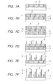
- Figs. 7A to 7F show this process, and in Fig. 7A, the pattern of the grating portions 2 by Al is made on the substrate 1, and the space between adjacent ones of these grating portions 2 is filled with the filling material 3 of SiO 2 . In Fig. 7B, the pattern of the grating portions 2 is again made thereon, and the space between adjacent ones of these grating portions 2 is filled with the filling material 3. In Fig. 7C, the same step as that of Fig. 7B is repeated to thereby manufacture a three-layer stacked structure. In Figs.
- a fluorine etchant is used and dry etching is effected on the filling material 3 with the grating portions 2 as a mask, whereupon finally, an optical element of the shape of Fig. 7F, i.e., the shape of Fig. 5 can be obtained.
- This third embodiment has the following effects, in addition to the effects of Embodiments 1 and 2.
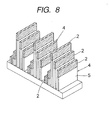
- Fig. 8 shows the construction of an optical element according to the fourth embodiment.
- the structure of this fourth embodiment is a fine-layer structure, and the manufacturing process thereof is the development of the process of the third embodiment.
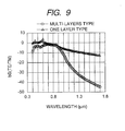
- the pitch P of the grating portions 2 is 0.6 ⁇ m, and the height d of the grating portions 2 is 0.18 ⁇ m, and the filling factor f is 0.1, and five layers are made, a characteristic of the quenching ratio such as is shown in Fig. 9 is obtained as the result of the simulation of RCWA.
- a line of circles indicates the characteristic of the quenching ratio ⁇ of the structure of the fourth embodiment
- a line of triangles indicates the characteristic of the quenching ratio ⁇ of a grating of one layer having a pitch of 0.6 ⁇ m.
- the quenching ratio ⁇ is improved from a wavelength of the order of 0.9 ⁇ m, and in the range of 1.1 ⁇ m, there is shown a characteristic usable at efficiency of -20dB or greater.
- This fourth embodiment has the following effects, in addition to the effects of the foregoing first, second and third embodiments.
- the optical element satisfies the following condition, assuming that the number of the layer is n, a pitch of the gratings (grating portions 2) in each layer is P and a filling factor is f. That is, f ⁇ P /(2 n ) .
- the above mentioned inventions in the first to forth embodiments can be used in a linear encoder as an optical measurement or an optical isolator as an optical communication device.
Landscapes
- Physics & Mathematics (AREA)
- General Physics & Mathematics (AREA)
- Optics & Photonics (AREA)
- Diffracting Gratings Or Hologram Optical Elements (AREA)
- Polarising Elements (AREA)
Abstract
Grating portions (2) made of metal are arranged as a first layer at regular intervals on a substrate (1), and a filling material (3) fills the space between adjacent ones of the grating portions (2). Also, as a second layer, grating portions (2) alone are similarly arranged at regular intervals on the filling material (3). Structures each comprising grating portions of a relatively great pitch (P) are stacked one upon the other to thereby cause them to function as a deflecting plate having a small apparent pitch.
Description
- This invention relates to an optical element for use in an optical apparatus for spectroscopy, optical measurement, optical communication, etc., a method of manufacturing the same, and an optical apparatus using the optical element.
- The range of wavelength used in optical communication, optical measurement, etc. is sub µm to 2µm.
- If, for light in this range of wavelength, an attempt is made to make the pitch P of a
grating 1/10 of the wavelength, the pitch P must be made smaller than 0.2µm, and apparatuses which can made it are restricted to EB and semiconductor exposure apparatus of the newest type ArF. - The former is poor in productivity, and the latter is high in price and is also high in maintenance cost. Also, when the visible light range is taken into consideration, the grating has to be a grating having a pitch P of the order of 40nm, and it is difficult to make such a grating even by the use of the aforementioned EB.
- It is an object of the present invention to solve the above-noted problem, and to stack a grating of a coarse pattern pitch while shifting the position thereof to thereby manufacture a grating apparently having a fine pitch.
- That is, it is an object of the present invention to provide an optical element which can improve the characteristic of a deflecting plate of an optical apparatus even by the use of a process of making a grating of a coarse pitch, and a method of manufacturing the same.
- In order to achieve the above object, a feature of the present invention is that an element for modulating the polarization of light is made into a periodic structure, which is stacked into two or more layers while the periodicity of the periodic structure is shifted.
- The present invention provides an optical element including:
- a substrate;
- a first periodic grating formed on said substrate and having a polarization property; and
- a second periodic grating shifted in position relative to said first periodic grating, and stacked on said first grating.
- The invention also provides a method of manufacturing an optical element, including:
- a first step of forming on a substrate an element for modulating the polarization of light in the form of a first periodic structure comprising the repetition of a dielectric material and an electrical conductor;
- a second step of stacking a second periodic structure on the periodic structure formed in said first step while shifting the periodicity thereof,
- the space between the dielectric material and dielectric material of each of said first and second periodic structures being filled with a filling material; and
- a third step of etching said filling material with said electrical conductor as a mask.
- A further feature of the present invention is that an element for modulating the polarization of light is made into a periodic structure by the repetition of a dielectric material and an electrical conductor, and the periodic structure is stacked into two or more layers while the periodicity of the periodic structure is shifted, and the dielectric material is etched with the electrical conductor as a mask.
- Thus, according to the present invention, even if the pitch of a grating is coarse, the apparent pitch becomes small by stacking and the polarization property can be improved.
-
- Fig. 1 shows the construction of a first embodiment.
- Fig. 2 is a characteristic graph of the quenching ratio.
- Fig. 3 shows the construction of a second embodiment.
- Fig. 4 is a characteristic graph of the quenching ratio.
- Fig. 5 shows the construction of a third embodiment.
- Fig. 6 is a characteristic graph of the quenching ratio.
- Figs. 7A, 7B, 7C, 7D, 7E and 7F show the steps of a manufacturing process.
- Fig. 8 shows the construction of a fourth embodiment.
- Fig. 9 is a characteristic graph of the quenching ratio.
- The present invention will hereinafter be described in detail with respect to some embodiments thereof shown in the drawings.
- Fig. 1 shows the construction of a fine optical element according to the first embodiment.
- Grating
portions 2 made of metal are arranged as a first layer at regular intervals on asubstrate 1, a fillingmaterial 3 fills the space between adjacent ones of thegrating portions 2. - Also, as a second layer, grating
portions 2 alone are similarly arranged at regular intervals on the fillingmaterial 3. - When the pitch P of the
grating portions 2 of height d on thesubstrate 1 is given a value smaller than the wavelength λ of light used, the gratingportions 2 function as deflecting plates. - When the pitch P of the grating
portions 2 is sufficiently small relative to the wavelength λ, the deflecting plates function best. However, they are still difficult to make by an actual machining technique. - So, by stacking a structure comprising grating
portions 2 of a relatively large pitch P, an approximation to the best performance is obtained. - In Fig. 1, the
grating portions 2 are stacked. For example, the pitch P=0.26µm and height d=150nm of thegrating portions 2 in the first layer, and thegrating portions 2 in the second layer are disposed while being shifted by P/2 in the pitch direction with respect to thegrating portions 2 in the first layer. - Al is used for the
grating portions 2, SiO2 is used for the fillingmaterial 3, and transparent synthetic quartz is used for thesubstrate 1. - The filling
material 3 can fill the space between adjacent ones of thegrating portions 2 in the second layer. - Fig. 2 shows the result of a simulation, evaluation being effected by the use of RCWA (Rigorous Coupled-Wave Analysis Method). It can be seen from Fig. 2 that the structure of two layers leads to the obtainment of a deflecting plate with a better quenching ratio γ. Here, the quenching ratio γ is defined by γ=10 Log10 (ITE/ITM), where ITE is the element transmitted light intensity of TE wave (light having polarization in the same direction as the direction of the grating line), and I™ is the element transmitted light intensity of TM wave (light having polarization in the same direction as the arrangement direction of the gratings).
- Also, if the refractive index of the filling
material 3 filling the space between adjacent ones of thegrating portions 2 as the first layer is small, the quenching ratio γ becomes great. - In the first embodiment, SiO2 has been described as an example of the
filling material 3, but if it is replaced with a film of MgF2, there can be constructed a deflecting plate greater in quenching ratio γ. - This first embodiment is very simple in construction, and is coarse in pattern and therefore, can be manufactured even if use is not made of a manufacturing apparatus at the most advanced level. Also, when manufacture is effected by the use of a semiconductor process or the like, size reduction, higher accuracy, lower costs and mass production become possible.
- By merely the construction of the film of the periodic structure member alone, or by providing it on thin film, it is possible to obtain an optical element much better in efficiency than a conventional one.
- Fig. 3 shows the construction of an optical element according to the second embodiment, and this construction is one in which two
transparent substrates 1 to which gratingportions 2 are fixed at regular intervals are fixed with the gratingportions 2 fixed in opposed relationship with one another. - The principle of the second embodiment is basically the same as that of the first embodiment. Unlike the first embodiment, however, the space between adjacent ones of the grating
portions 2 in the first layer is filled with air which has a small refractive index, to thereby improve the quenching ratio γ. - If here, the pitch P of the
grating portions 2 is 0.26µm, and the height d of thegrating portions 2 is 0.15µm, and the filling factor f is 0.15, a characteristic of the quenching ratio γ such as is shown in Fig. 4 is obtained as the result of the simulation of RCWA. - In Fig. 4, points indicated by triangles represent the characteristic of the quenching ratio γ of a conventional grid wire deflecting plate (the pitch P=0.26µm, the height d of the grating =0.15µm, the filling factor f=0.3) relative to the wavelength when it has one layer of
grating portions 2. - Also, points indicated by circles represent the characteristic of the quenching ratio γ of the first embodiment, and points indicated by rectangles represent the characteristic of the quenching ratio γ of the second embodiment.
- If the space between adjacent ones of the
grating portions 2 in the first layer is not filled with the fillingmaterial 3, it becomes difficult to form a structure in the upper portion thereof, but as shown in Fig. 3, two elements have only one layer of gratingportions 2, and they are stacked one upon the other with the grating portions opposed to each other, as a result, the manufacture of this structure becomes possible. - This second embodiment has the following effects, in addition to the effects of the first embodiment.
- (1) The substance between adjacent ones of the
grating portions 2 in the first layer is air or the like which has a low refractive index and therefore, the quenching ratio γ is good. - (2) The structures are manufactured and stuck together, whereby a stacked structure can be manufactured simply.
- Fig. 5 shows the construction of an optical element according to the third embodiment, in which on a
substrate 1, there are arranged at regularintervals wall portions 4 provided withgrating portions 2 on the uppermost portions thereof and having three different heights. - Supporting
portions 5 supporting thegrating portions 2 are made of SiO2. - Also, the
wall portions 4 having three different heights are arranged in order of height, and combinations of the threewall portions 4 are repeatedly arranged. - The principle of this third embodiment is also basically the same as that of the first embodiment. The portions other than the SiO2 layers providing the supporting
portions 5 under thegrating portions 2 in the upper layer are air and therefore, the actual average refractive index becomes smaller than the refractive index of SiO2. Therefore, the quenching ratio γ of the stacked structures is improved. - Here, the pitch P of the
grating portions 2 is 0.26µm, the height d of thegrating portions 2 is 0.18µm, the filling factor f is 0.15, and three layers are provided as shown in Fig. 5. As the result of the simulation of RCWA, there is obtained a characteristic of the quenching ratio γ such as is shown in Fig. 6. - Triangles in Fig. 6 represent the characteristic of the quenching ratio γ of a conventional grid wire deflecting plate (the pitch P=0.26µm, the height d of the grating =0.18µm, the filling factor f=0.3) relative to the wavelength, and points indicated by circles represent the characteristic of the quenching ratio γ of this third embodiment.
- If the space between adjacent ones of the
grating portions 2 in the first layer is not filled with the filling material, it becomes possible to form a structure thereon, but periodic structures each comprising three layers of gratingportions 2 and the fillingmaterial 3 are stacked, and the fillingmaterial 3 of this stacked structure is etched until thesubstrate 1 appears, as a result this structure can be manufactured easily. - Also, Al and SiO2 differ as to the etchant during etching and therefore, the
grating portions 2 in the Al portion can be caused to act as a mask when SiO2 of the supportingportions 5 is etched. - Figs. 7A to 7F show this process, and in Fig. 7A, the pattern of the
grating portions 2 by Al is made on thesubstrate 1, and the space between adjacent ones of thesegrating portions 2 is filled with the fillingmaterial 3 of SiO2. In Fig. 7B, the pattern of thegrating portions 2 is again made thereon, and the space between adjacent ones of thesegrating portions 2 is filled with the fillingmaterial 3. In Fig. 7C, the same step as that of Fig. 7B is repeated to thereby manufacture a three-layer stacked structure. In Figs. 7D to 7D, a fluorine etchant is used and dry etching is effected on the fillingmaterial 3 with thegrating portions 2 as a mask, whereupon finally, an optical element of the shape of Fig. 7F, i.e., the shape of Fig. 5 can be obtained. - This third embodiment has the following effects, in addition to the effects of
Embodiments - (1) the third embodiment is of a simple construction, and if dry etching or the like is used, the final shape can be easily formed.
- (2) the third embodiment is of e.g. a three-layer construction and therefore, the apparent pitch becomes fine, and there is obtained a deflecting plate having a good quenching ratio γ.
- Fig. 8 shows the construction of an optical element according to the fourth embodiment.
- The structure of this fourth embodiment is a fine-layer structure, and the manufacturing process thereof is the development of the process of the third embodiment.
- If here, the pitch P of the
grating portions 2 is 0.6µm, and the height d of thegrating portions 2 is 0.18µm, and the filling factor f is 0.1, and five layers are made, a characteristic of the quenching ratio such as is shown in Fig. 9 is obtained as the result of the simulation of RCWA. - In Fig. 9, a line of circles indicates the characteristic of the quenching ratio γ of the structure of the fourth embodiment, and a line of triangles indicates the characteristic of the quenching ratio γ of a grating of one layer having a pitch of 0.6µm.
- According to the fourth embodiment, the quenching ratio γ is improved from a wavelength of the order of 0.9µm, and in the range of 1.1µm, there is shown a characteristic usable at efficiency of -20dB or greater.
- This fourth embodiment has the following effects, in addition to the effects of the foregoing first, second and third embodiments.
- (1) the fourth embodiment is of a simple construction, and if dry etching or the like is used, the final shape can be simple formed.
- (2) the fourth embodiment is of a five-layer construction and therefore, in spite of the pitch of one layer being greater than the wavelength, the apparent pitch becomes that for the five-layer construction, and it becomes possible to easily manufacture a deflecting plate having a good quenching ratio γ.
- According to the above-mentioned embodiments, the optical element satisfies the following condition, assuming that the number of the layer is n, a pitch of the gratings (grating portions 2) in each layer is P and a filling factor is f. That is, f ≤ P/(2n).
- Moreover, the above mentioned inventions in the first to forth embodiments can be used in a linear encoder as an optical measurement or an optical isolator as an optical communication device.
Claims (9)
- An optical element including:a substrate;a first periodic gratings formed on said substrate and having a polarization property as a first layer; anda second periodic grating shifted in position relative to said first periodic grating as a second layer, and stacked on said first grating.
- An optical element according to Claim 1, wherein said first and second periodic gratings are disposed at regular intervals in each layer.
- An optical element according to Claim 1, the cross sections of said first and second periodic gratings are rectangular.
- An optical element according to Claim 1, wherein said first and second periodic gratings are formed of a metal material.
- An optical element according to Claim 1, wherein said first layer is constituted by the repetition of a dielectric material and an electrical conductor.
- An optical element according to Claim 1, wherein the periods of said first and second periodic elements are shorter than a wavelength used.
- An optical element according to Claim 1, wherein assuming that the number of the layer is n, a pitch of the gratings in each layer is P and a filling factor is f, the following condition is satisfied:

- An optical apparatus using an optical element according to any one of Claims 1 to 7.
- A method of manufacturing an optical element, including:a first step of forming on a substrate an element for modulating the polarization of light in the form of a first periodic structure comprising the repetition of a dielectric material and an electrical conductor;a second step of stacking a second periodic structure on the periodic structure formed in said first step while shifting the periodicity thereof,the space between the dielectric material and dielectric material of each of said first and second periodic structures being filled with a filling material; anda third step of etching said filling material with said electrical conductor as a mask.
Applications Claiming Priority (1)
| Application Number | Priority Date | Filing Date | Title |
|---|---|---|---|
| JP2004358594A JP2006163291A (en) | 2004-12-10 | 2004-12-10 | Optical element and manufacturing method thereof |
Publications (1)
| Publication Number | Publication Date |
|---|---|
| EP1669780A1 true EP1669780A1 (en) | 2006-06-14 |
Family
ID=35976666
Family Applications (1)
| Application Number | Title | Priority Date | Filing Date |
|---|---|---|---|
| EP05257609A Withdrawn EP1669780A1 (en) | 2004-12-10 | 2005-12-12 | Optical element, method of manufacturing same, and optical apparatus using optical element |
Country Status (3)
| Country | Link |
|---|---|
| US (1) | US20060126699A1 (en) |
| EP (1) | EP1669780A1 (en) |
| JP (1) | JP2006163291A (en) |
Cited By (3)
| Publication number | Priority date | Publication date | Assignee | Title |
|---|---|---|---|---|
| US8493658B2 (en) | 2007-07-06 | 2013-07-23 | Semiconductor Energy Laboratory Co., Ltd. | Polarizer and display device including polarizer |
| CN105785493A (en) * | 2016-05-09 | 2016-07-20 | 深圳市华星光电技术有限公司 | Metal grating polaroid and manufacturing method therefor |
| CN108132496A (en) * | 2017-12-28 | 2018-06-08 | 深圳市华星光电技术有限公司 | Metal gate polaroid and preparation method thereof, liquid crystal display panel and liquid crystal display |
Families Citing this family (16)
| Publication number | Priority date | Publication date | Assignee | Title |
|---|---|---|---|---|
| US7674573B2 (en) * | 2006-08-08 | 2010-03-09 | Canon Kabushiki Kaisha | Method for manufacturing layered periodic structures |
| JP5069037B2 (en) * | 2007-04-16 | 2012-11-07 | 旭化成イーマテリアルズ株式会社 | Laminated wire grid polarizer |
| JP4535121B2 (en) * | 2007-11-28 | 2010-09-01 | セイコーエプソン株式会社 | OPTICAL ELEMENT AND ITS MANUFACTURING METHOD, LIQUID CRYSTAL DEVICE, ELECTRONIC DEVICE |
| JP5339975B2 (en) | 2008-03-13 | 2013-11-13 | キヤノン株式会社 | Phase grating used for X-ray phase imaging, X-ray phase contrast image imaging apparatus using the phase grating, X-ray computed tomography system |
| JP5527074B2 (en) * | 2009-11-16 | 2014-06-18 | セイコーエプソン株式会社 | Polarizing element and projector |
| JP5526851B2 (en) * | 2010-02-19 | 2014-06-18 | セイコーエプソン株式会社 | Polarizing element and projector |
| JP5463947B2 (en) * | 2010-02-19 | 2014-04-09 | セイコーエプソン株式会社 | Polarizing element and projector |
| JP6256966B2 (en) * | 2012-10-05 | 2018-01-10 | 公立大学法人大阪市立大学 | Multilayer wire grid and manufacturing method thereof |
| JP2015219319A (en) * | 2014-05-15 | 2015-12-07 | デクセリアルズ株式会社 | Inorganic polarizer and method for manufacturing the same |
| US11231544B2 (en) * | 2015-11-06 | 2022-01-25 | Magic Leap, Inc. | Metasurfaces for redirecting light and methods for fabricating |
| JP6961619B2 (en) | 2016-05-06 | 2021-11-05 | マジック リープ, インコーポレイテッドMagic Leap, Inc. | Meta-surface with asymmetric lattice for redirecting light and manufacturing method |
| IL307294A (en) | 2017-01-27 | 2023-11-01 | Magic Leap Inc | Diffraction gratings formed by metasurfaces having differently oriented nanobeams |
| WO2018140502A1 (en) | 2017-01-27 | 2018-08-02 | Magic Leap, Inc. | Antireflection coatings for metasurfaces |
| CN113031139B (en) * | 2019-12-25 | 2022-07-05 | 南开大学 | A 3D printed transmissive large-angle deflection double-layer uniform grating |
| JP7809696B2 (en) | 2020-09-16 | 2026-02-02 | マジック リープ, インコーポレイテッド | Eyepiece for Augmented Reality Display System |
| JP7579727B2 (en) * | 2021-03-19 | 2024-11-08 | シチズンファインデバイス株式会社 | Optical unit design method |
Citations (5)
| Publication number | Priority date | Publication date | Assignee | Title |
|---|---|---|---|---|
| US4289381A (en) * | 1979-07-02 | 1981-09-15 | Hughes Aircraft Company | High selectivity thin film polarizer |
| JPS6066203A (en) * | 1983-09-22 | 1985-04-16 | Matsushita Electric Ind Co Ltd | Polarizing element |
| WO2000079317A1 (en) * | 1999-06-22 | 2000-12-28 | Moxtek | Broadband wire grid polarizer for the visible spectrum |
| JP2003066229A (en) * | 2001-08-28 | 2003-03-05 | Kyocera Corp | Striped polarizer |
| WO2004019070A2 (en) * | 2002-08-21 | 2004-03-04 | Nanoopto Corporation | Method and system for providing beam polarization |
Family Cites Families (14)
| Publication number | Priority date | Publication date | Assignee | Title |
|---|---|---|---|---|
| US4514479A (en) * | 1980-07-01 | 1985-04-30 | The United States Of America As Represented By The Secretary Of The Navy | Method of making near infrared polarizers |
| DE3605516A1 (en) * | 1985-02-21 | 1986-09-04 | Canon K.K., Tokio/Tokyo | OPTICAL FUNCTIONAL ELEMENT AND OPTICAL FUNCTIONAL DEVICE |
| JP2973254B2 (en) * | 1991-10-15 | 1999-11-08 | 京セラ株式会社 | Birefringent structure |
| JP4365927B2 (en) * | 1999-03-12 | 2009-11-18 | キヤノン株式会社 | Interference measuring device and grating interference encoder |
| DE60033075T3 (en) * | 1999-04-16 | 2012-08-30 | Canon K.K. | encoder |
| JP2000321021A (en) * | 1999-05-10 | 2000-11-24 | Canon Inc | Interfering device, displacement measuring device, and information recording and / or reproducing device using the same |
| JP2001076325A (en) * | 1999-09-07 | 2001-03-23 | Canon Inc | Displacement detection device and information recording device |
| US6714350B2 (en) * | 2001-10-15 | 2004-03-30 | Eastman Kodak Company | Double sided wire grid polarizer |
| JP4116305B2 (en) * | 2002-02-26 | 2008-07-09 | 株式会社リコー | Wave plate, wave plate unit, optical pickup device, and optical disk device |
| JP2003255113A (en) * | 2002-02-28 | 2003-09-10 | Canon Inc | Optical separation element and optical device using the same |
| JP2004045672A (en) * | 2002-07-11 | 2004-02-12 | Canon Inc | Polarization separation element and optical system using the same |
| JP2004309903A (en) * | 2003-04-09 | 2004-11-04 | Ricoh Opt Ind Co Ltd | Inorganic polarizing element, polarizing optical element, and liquid crystal element |
| TWI223103B (en) * | 2003-10-23 | 2004-11-01 | Ind Tech Res Inst | Wire grid polarizer with double metal layers |
| US7570424B2 (en) * | 2004-12-06 | 2009-08-04 | Moxtek, Inc. | Multilayer wire-grid polarizer |
-
2004
- 2004-12-10 JP JP2004358594A patent/JP2006163291A/en active Pending
-
2005
- 2005-12-08 US US11/298,425 patent/US20060126699A1/en not_active Abandoned
- 2005-12-12 EP EP05257609A patent/EP1669780A1/en not_active Withdrawn
Patent Citations (5)
| Publication number | Priority date | Publication date | Assignee | Title |
|---|---|---|---|---|
| US4289381A (en) * | 1979-07-02 | 1981-09-15 | Hughes Aircraft Company | High selectivity thin film polarizer |
| JPS6066203A (en) * | 1983-09-22 | 1985-04-16 | Matsushita Electric Ind Co Ltd | Polarizing element |
| WO2000079317A1 (en) * | 1999-06-22 | 2000-12-28 | Moxtek | Broadband wire grid polarizer for the visible spectrum |
| JP2003066229A (en) * | 2001-08-28 | 2003-03-05 | Kyocera Corp | Striped polarizer |
| WO2004019070A2 (en) * | 2002-08-21 | 2004-03-04 | Nanoopto Corporation | Method and system for providing beam polarization |
Non-Patent Citations (3)
| Title |
|---|
| PATENT ABSTRACTS OF JAPAN vol. 009, no. 203 (P - 381) 21 August 1985 (1985-08-21) * |
| PATENT ABSTRACTS OF JAPAN vol. 2003, no. 07 3 July 2003 (2003-07-03) * |
| YU ZHAONING ET AL: "Reflective polarizer based on a stacked double-layer subwavelength metal grating structure fabricated using nanoimprint lithography", APPLIED PHYSICS LETTERS, AIP, AMERICAN INSTITUTE OF PHYSICS, MELVILLE, NY, US, vol. 77, no. 7, 14 August 2000 (2000-08-14), pages 927 - 929, XP012027261, ISSN: 0003-6951 * |
Cited By (5)
| Publication number | Priority date | Publication date | Assignee | Title |
|---|---|---|---|---|
| US8493658B2 (en) | 2007-07-06 | 2013-07-23 | Semiconductor Energy Laboratory Co., Ltd. | Polarizer and display device including polarizer |
| CN105785493A (en) * | 2016-05-09 | 2016-07-20 | 深圳市华星光电技术有限公司 | Metal grating polaroid and manufacturing method therefor |
| WO2017193445A1 (en) * | 2016-05-09 | 2017-11-16 | 深圳市华星光电技术有限公司 | Metal grating polariser and manufacturing method therefor |
| CN105785493B (en) * | 2016-05-09 | 2019-01-22 | 深圳市华星光电技术有限公司 | Metal grating polaroid and preparation method thereof |
| CN108132496A (en) * | 2017-12-28 | 2018-06-08 | 深圳市华星光电技术有限公司 | Metal gate polaroid and preparation method thereof, liquid crystal display panel and liquid crystal display |
Also Published As
| Publication number | Publication date |
|---|---|
| US20060126699A1 (en) | 2006-06-15 |
| JP2006163291A (en) | 2006-06-22 |
Similar Documents
| Publication | Publication Date | Title |
|---|---|---|
| EP1669780A1 (en) | Optical element, method of manufacturing same, and optical apparatus using optical element | |
| US20210018851A1 (en) | Overlay measurement structures and method of overlay errors | |
| DE602005000684T2 (en) | Photoelectric position sensor and method for producing gratings | |
| EP0742455B1 (en) | Scale, method of fabricating a scale and a position measuring device | |
| JP4800437B2 (en) | Broadband wire grid polarizer for the visible spectrum | |
| EP2237332B1 (en) | Light emitting device | |
| JP4905454B2 (en) | Metal plate for wire grid, wire grid, and method for manufacturing metal plate for wire grid | |
| US20150171244A1 (en) | Light absorption and filtering properties of vertically oriented semiconductor nano wires | |
| US20100091369A1 (en) | Double-layer grating | |
| US20210200106A1 (en) | Improved self-moire grating design for use in metrology | |
| US6922287B2 (en) | Light coupling element | |
| JP2019120500A (en) | Scale and method for manufacturing the same | |
| JP5450449B2 (en) | Optical sheet, light emitting device, and optical sheet manufacturing method | |
| EP2103974A1 (en) | Optical waveguide having grating and method of forming the same | |
| CN102711303A (en) | Panel, light emitting device and method for manufacturing panel | |
| US20050233228A1 (en) | Grayscale lithography methods and devices | |
| JP2001272566A (en) | Method for manufacturing photonic crystal | |
| JP2005019789A (en) | Semiconductor device | |
| JP4677276B2 (en) | Method for producing three-dimensional photonic crystal | |
| DE112012004119B4 (en) | Spectroscopic sensor | |
| DE112012004131T5 (en) | Manufacturing method for a spectroscopic sensor | |
| EP2199837B1 (en) | A dispersion grating | |
| JP2011075850A (en) | Multilayer film laminar diffraction grating and spectrometer | |
| JP5080227B2 (en) | Optical waveguide device and manufacturing method thereof | |
| KR102168744B1 (en) | Wire Grid Polarizer |
Legal Events
| Date | Code | Title | Description |
|---|---|---|---|
| PUAI | Public reference made under article 153(3) epc to a published international application that has entered the european phase |
Free format text: ORIGINAL CODE: 0009012 |
|
| AK | Designated contracting states |
Kind code of ref document: A1 Designated state(s): AT BE BG CH CY CZ DE DK EE ES FI FR GB GR HU IE IS IT LI LT LU LV MC NL PL PT RO SE SI SK TR |
|
| AX | Request for extension of the european patent |
Extension state: AL BA HR MK YU |
|
| AKX | Designation fees paid | ||
| REG | Reference to a national code |
Ref country code: DE Ref legal event code: 8566 |
|
| 18D | Application deemed to be withdrawn |
Effective date: 20061215 |