EP1666894A1 - Current sensor - Google Patents
Current sensor Download PDFInfo
- Publication number
- EP1666894A1 EP1666894A1 EP05025790A EP05025790A EP1666894A1 EP 1666894 A1 EP1666894 A1 EP 1666894A1 EP 05025790 A EP05025790 A EP 05025790A EP 05025790 A EP05025790 A EP 05025790A EP 1666894 A1 EP1666894 A1 EP 1666894A1
- Authority
- EP
- European Patent Office
- Prior art keywords
- current
- magnetoresistive
- current sensor
- magnetic field
- patterns
- Prior art date
- Legal status (The legal status is an assumption and is not a legal conclusion. Google has not performed a legal analysis and makes no representation as to the accuracy of the status listed.)
- Withdrawn
Links
- 230000005291 magnetic effect Effects 0.000 claims abstract description 110
- 239000010409 thin film Substances 0.000 claims abstract description 51
- 238000004804 winding Methods 0.000 claims abstract description 35
- 230000008859 change Effects 0.000 claims description 49
- 239000010408 film Substances 0.000 claims description 37
- 230000005415 magnetization Effects 0.000 claims description 30
- 230000035945 sensitivity Effects 0.000 abstract description 6
- 230000007423 decrease Effects 0.000 description 10
- 238000000034 method Methods 0.000 description 9
- 238000010586 diagram Methods 0.000 description 8
- 239000010949 copper Substances 0.000 description 7
- 238000004891 communication Methods 0.000 description 6
- 238000005259 measurement Methods 0.000 description 5
- RYGMFSIKBFXOCR-UHFFFAOYSA-N Copper Chemical compound [Cu] RYGMFSIKBFXOCR-UHFFFAOYSA-N 0.000 description 4
- 239000004020 conductor Substances 0.000 description 4
- 229910052802 copper Inorganic materials 0.000 description 4
- 238000001514 detection method Methods 0.000 description 4
- 238000010438 heat treatment Methods 0.000 description 4
- 230000009471 action Effects 0.000 description 3
- 230000005290 antiferromagnetic effect Effects 0.000 description 3
- TWNQGVIAIRXVLR-UHFFFAOYSA-N oxo(oxoalumanyloxy)alumane Chemical compound O=[Al]O[Al]=O TWNQGVIAIRXVLR-UHFFFAOYSA-N 0.000 description 3
- 229910001030 Iron–nickel alloy Inorganic materials 0.000 description 2
- 229910000914 Mn alloy Inorganic materials 0.000 description 2
- 230000002411 adverse Effects 0.000 description 2
- 230000003247 decreasing effect Effects 0.000 description 2
- 239000010931 gold Substances 0.000 description 2
- 239000007769 metal material Substances 0.000 description 2
- 238000004544 sputter deposition Methods 0.000 description 2
- 229910003321 CoFe Inorganic materials 0.000 description 1
- 229910001313 Cobalt-iron alloy Inorganic materials 0.000 description 1
- XUIMIQQOPSSXEZ-UHFFFAOYSA-N Silicon Chemical compound [Si] XUIMIQQOPSSXEZ-UHFFFAOYSA-N 0.000 description 1
- 239000002885 antiferromagnetic material Substances 0.000 description 1
- 229910017052 cobalt Inorganic materials 0.000 description 1
- 239000010941 cobalt Substances 0.000 description 1
- GUTLYIVDDKVIGB-UHFFFAOYSA-N cobalt atom Chemical compound [Co] GUTLYIVDDKVIGB-UHFFFAOYSA-N 0.000 description 1
- 230000002950 deficient Effects 0.000 description 1
- 230000006866 deterioration Effects 0.000 description 1
- 230000000694 effects Effects 0.000 description 1
- 239000003302 ferromagnetic material Substances 0.000 description 1
- 230000004907 flux Effects 0.000 description 1
- PCHJSUWPFVWCPO-UHFFFAOYSA-N gold Chemical compound [Au] PCHJSUWPFVWCPO-UHFFFAOYSA-N 0.000 description 1
- 229910052737 gold Inorganic materials 0.000 description 1
- 230000006872 improvement Effects 0.000 description 1
- 238000007689 inspection Methods 0.000 description 1
- 238000009413 insulation Methods 0.000 description 1
- SHMWNGFNWYELHA-UHFFFAOYSA-N iridium manganese Chemical compound [Mn].[Ir] SHMWNGFNWYELHA-UHFFFAOYSA-N 0.000 description 1
- 230000007774 longterm Effects 0.000 description 1
- 230000005381 magnetic domain Effects 0.000 description 1
- 239000000696 magnetic material Substances 0.000 description 1
- IGOJMROYPFZEOR-UHFFFAOYSA-N manganese platinum Chemical compound [Mn].[Pt] IGOJMROYPFZEOR-UHFFFAOYSA-N 0.000 description 1
- 229910052751 metal Inorganic materials 0.000 description 1
- 239000002184 metal Substances 0.000 description 1
- 230000004048 modification Effects 0.000 description 1
- 238000012986 modification Methods 0.000 description 1
- 238000005457 optimization Methods 0.000 description 1
- 230000004043 responsiveness Effects 0.000 description 1
- 229910052710 silicon Inorganic materials 0.000 description 1
- 239000010703 silicon Substances 0.000 description 1
- 239000000758 substrate Substances 0.000 description 1
Images





Classifications
-
- G—PHYSICS
- G01—MEASURING; TESTING
- G01R—MEASURING ELECTRIC VARIABLES; MEASURING MAGNETIC VARIABLES
- G01R33/00—Arrangements or instruments for measuring magnetic variables
- G01R33/02—Measuring direction or magnitude of magnetic fields or magnetic flux
- G01R33/06—Measuring direction or magnitude of magnetic fields or magnetic flux using galvano-magnetic devices
- G01R33/09—Magnetoresistive devices
- G01R33/093—Magnetoresistive devices using multilayer structures, e.g. giant magnetoresistance sensors
-
- B—PERFORMING OPERATIONS; TRANSPORTING
- B82—NANOTECHNOLOGY
- B82Y—SPECIFIC USES OR APPLICATIONS OF NANOSTRUCTURES; MEASUREMENT OR ANALYSIS OF NANOSTRUCTURES; MANUFACTURE OR TREATMENT OF NANOSTRUCTURES
- B82Y25/00—Nanomagnetism, e.g. magnetoimpedance, anisotropic magnetoresistance, giant magnetoresistance or tunneling magnetoresistance
-
- G—PHYSICS
- G01—MEASURING; TESTING
- G01R—MEASURING ELECTRIC VARIABLES; MEASURING MAGNETIC VARIABLES
- G01R15/00—Details of measuring arrangements of the types provided for in groups G01R17/00 - G01R29/00, G01R33/00 - G01R33/26 or G01R35/00
- G01R15/14—Adaptations providing voltage or current isolation, e.g. for high-voltage or high-current networks
- G01R15/20—Adaptations providing voltage or current isolation, e.g. for high-voltage or high-current networks using galvano-magnetic devices, e.g. Hall-effect devices, i.e. measuring a magnetic field via the interaction between a current and a magnetic field, e.g. magneto resistive or Hall effect devices
- G01R15/205—Adaptations providing voltage or current isolation, e.g. for high-voltage or high-current networks using galvano-magnetic devices, e.g. Hall-effect devices, i.e. measuring a magnetic field via the interaction between a current and a magnetic field, e.g. magneto resistive or Hall effect devices using magneto-resistance devices, e.g. field plates
Definitions
- the present invention relates to a small-sized current sensor capable of sensing a change in current flowing in a conductor with high sensitivity.
- a method of connecting resistors in series in the circuit and measuring a voltage drop in the resistors is used.
- a load different from that in a communication system is applied, and there is the possibility that an adverse influence is exerted on the communication system.
- a method of indirectly measuring a signal current by detecting the gradient of a current magnetic field generated by the signal current (while maintaining an insulated state so that direct current does not flow) is used. Examples of such a method are a method of using a transformer in which coils are connected to each other and a method using a photocoupler.
- a signal current which is an alternate current can be transmitted
- a signal current which is a direct current cannot be transmitted.
- a frequency band in which the signal current as the direct current can be transmitted is limited.
- an impedance of the transformer changes, so that it lacks linearity, and an adverse influence may be exerted on the communication device and the like.
- the photocoupler has excellent frequency characteristics, but it is difficult to reduce the size when the photocoupler is used. There is also a problem such that, in long terms, deterioration in a signal intensity caused by a change with time tends to occur.
- GMR element giant magnetoresistive element
- a current sensor using such a GMR element has an excellent detection sensitivity and responsiveness and can obtain detection characteristics which are stable also against a temperature change.
- a current sensor capable of detecting a weaker current and having a more compact general configuration is being demanded.
- a GMR element is provided so as to be adjacent to a line to be measured in an in-plane direction, so that it is difficult to detect a weak current and it is disadvantageous from the viewpoint of miniaturization.
- the present invention has been achieved in consideration of such problems, and an object of the invention is to provide a current sensor capable of measuring a current to be detected with high precision while realizing a compact configuration.
- a current sensor of the present invention has the following components (A) to (C).
- the strip shape denotes here a shape whose dimension in the first direction is larger than dimension in the second direction.
- the first and second magnetoresistive elements and the first thin film coil are provided so as to be adjacent to each other in an in-plane direction, the first and second magnetoresistive elements are disposed more closely to the first thin film coil. Consequently, the dimensions of the whole are reduced and, moreover, a first current magnetic field based on the current to be detected which flows in the first thin film coil is applied to each of the element patterns of the first and second magnetoresistive elements more strongly.
- the first current magnetic field generated by the winding body portions of the first thin film coil corresponding to the element patterns of the first and second magnetoresistive elements is applied to each of the element patterns of the first and second magnetoresistive elements.
- the positions and the sectional dimensions in a section orthogonal to the first direction are easily optimized from the viewpoint of heating by the coil and a current efficiency of coil magnetic field strength.
- the first current magnetic field can be efficiently applied to each of the element patterns.
- the current sensor of the invention is constructed so that the resistance values of the first and second magnetoresistive elements change in directions opposite to each other in accordance with the first current magnetic field.
- the current sensor of the invention further includes: a third magnetoresistive element which includes a plurality of strip-shaped element patterns extending in the first direction and disposed so as to be adjacent to each other in the second direction, and which is formed in a region other than a region where the first magnetoresistive element at the first level is formed so as to be connected in series to the first magnetoresistive element; a fourth magnetoresistive element which includes a plurality of strip-shaped element patterns extending in the first direction and disposed so as to be adjacent to each other in the second direction and which is formed in a region other than a region where the second magnetoresistive element at the second level is formed so as to be connected in series to the second magnetoresistive element; and a second thin film coil which winds in a region other than a region where the first thin film coil at the third level is formed so as to include a plurality of winding body portions extending in the first direction in correspondence with the element patterns of the third and fourth magnetoresistive elements, and which applies a second current
- a resistance value of the second magnetoresistive element changes in the direction opposite to that of the first magnetoresistive element in accordance with the first current magnetic field
- a resistance value of the third magnetoresistive element changes in the direction opposite to that of the first magnetoresistive element generated by the first current magnetic field in accordance with the second current magnetic field
- a resistance value of the fourth magnetoresistive element changes in the same direction as that of the first magnetoresistive element generated by the first current magnetic field in accordance with the second current magnetic field.
- a bridge circuit may be constructed in such a manner that one end of the first magnetoresistive element and one end of the second magnetoresistive element are connected to each other at a first connection point, one end of the third magnetoresistive element and one end of the fourth magnetoresistive element are connected to each other at a second connection point, further, the other end of the first magnetoresistive element and the other end of the fourth magnetoresistive element are connected to each other at a third connection point, and the other end of the second magnetoresistive element and the other end of the third magnetoresistive element are connected to each other at a fourth connection point and, on the basis of a potential difference between the third and fourth connection points occurring when a voltage is applied across the first and second connection points, the current to be detected is detected.
- the element patterns in each of the first to fourth magnetoresistive elements may be connected in parallel to each other or in series to each other.
- each of the element patterns in the first to fourth magnetoresistive elements has a magnetization pinned film magnetized in the first direction.
- each of the element patterns in the first to fourth magnetoresistive elements be constructed so that the longitudinal dimension along the first direction is 10 times to 200 times as large as the width dimension along the second direction.
- the width dimension along the second direction is preferably in a range from 0.5 ⁇ m to 2.0 ⁇ m.
- each of the winding body portions in the first and second thin film coils have a section area which is from 0.4 ⁇ m 2 to 2.0 ⁇ m 2 in a cross section orthogonal to the first direction.
- the winding body portion has a width dimension in a range from 0.8 ⁇ m to 3.0 ⁇ m and a thickness dimension in a range from 0.2 ⁇ m to 1.4 ⁇ m.
- the current sensor includes: first and second magnetoresistive elements including a plurality of strip-shaped element patterns extending at the first and second levels, respectively; and a first thin film coil which winds at a third level while including a plurality of winding body portions corresponding to the element patterns of the first and second magnetoresistive elements, and which applies a first current magnetic field to each of the element patterns of the first and second magnetoresistive elements when a current to be detected is supplied.
- first and second magnetoresistive elements including a plurality of strip-shaped element patterns extending at the first and second levels, respectively
- a first thin film coil which winds at a third level while including a plurality of winding body portions corresponding to the element patterns of the first and second magnetoresistive elements, and which applies a first current magnetic field to each of the element patterns of the first and second magnetoresistive elements when a current to be detected is supplied.
- the resistance value as a whole can be suppressed to be relatively low without decreasing the resistance change ratio in the first magnetoresistive element, and a heating value of the first magnetoresistive element at the time of use can be reduced. Moreover, the influence of noise from the outside (unnecessary magnetic fields) is reduced, and the S/N ratio can be improved.
- the element patterns are connected in series to each other, without increasing the dimension in the first direction, the total length of the element patterns functioning as magnetosensitive parts can be increased, and the absolute value of the resistance value (impedance) of the whole in the first magnetoresistive element can be made larger. Therefore, even a weaker current to be detected can be measured with high precision.
- the current sensor of the invention includes, in addition to the first and second magnetoresistive elements and the first thin film coil, the third magnetoresistive element formed at the first level so as to be connected in series to the first magnetoresistive element, the fourth magnetoresistive element formed at the second level so as to be connected in series to the second magnetoresistive element, and the second thin film coil for applying the current magnetic field to each of the element patterns of the third and fourth magnetoresistive elements, the current to be detected is measured by using the four magnetoresistive elements. Consequently, the reliability of a measurement values of the current to be detected is improved more than the case of using two magnetoresistive elements. In this case, if a bridge circuit is constructed by using first to fourth magnetoresistive elements, the influence of variations in the characteristics among the magnetoresistive elements is reduced. Accordingly, the precision of the measurement can be further increased.
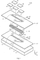
- Fig. 1 is a schematic view illustrating a perspective configuration of a current sensor 1 of the first embodiment.
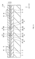
- Fig. 2 is a cross section taken along line II-II of the current sensor 1 illustrated in Fig. 1 seen from the direction indicated by the arrows (-X direction).
- the current sensor 1 is mounted on, for example, a communication device and is used for accurately measuring a current as a control signal.
- the current sensor in the first embodiment will be called a current sensor 1A.
- the current sensor 1A has a configuration obtained by sequentially stacking, on a substrate 2 made of silicon (Si) or the like via a base film 3 made of aluminum oxide (Al 2 O 3 ) or the like, a first level L1 including a first magnetoresistive element 21 (hereinbelow, simply called the MR element 21), a third level L3 including a first thin film coil 31(hereinbelow, simply called the thin film coil 31), and a second level L2 including a second magnetoresistive element 22 (hereinbelow, simply called the MR element 22).
- the MR element 21 has two element patterns 21A and 21B extending in a first direction (X axis direction) at the first level L1.
- the MR element 22 has two element patterns 22A and 22B extending in the X axis direction at the second level L2. Further, the thin film coil 31 winds at the third level L3 while including a winding body portion 31A extending in the X axis direction in correspondence with each of the element patterns 21A and 22A and a winding body portion 31B extending in the X axis direction in correspondence with each of the element patterns 21B and 22B.
- the MR element 21, the thin film coil 31, and the MR element 22 are covered with insulating films Z1 to Z3 made of Al 2 O 3 or the like, respectively, and electrically insulated from each other. Moreover, a plurality of electrode films 41 to 44 (shown in Fig. 1) are provided on the insulating film Z3.
- the thin film coil 31 is a thin film pattern made of a metal material having high conductivity such as copper (Cu), and to which a current Im to be detected such as a control signal or the like is supplied.
- a current Im to be detected such as a control signal or the like is supplied.
- one end 31S is connected to the electrode film 41 via a contact layer (not shown) and the other end 31E is connected to the electrode film 42 via a contact layer (not shown)(refer to Fig. 1).
- the current sensor 1A is set so that the current Im to be detected flows from the end 31S to the end 31E.
- the element patterns 21A and 21B and the element patterns 22A and 22B detect first current magnetic fields Hm1 (which will be described later) generated by a current Im to be detected, and which are provided in areas corresponding to the winding body portions 31A and 31B of the thin film coil 31 in the stacking direction, respectively.
- the element patterns 21A and 21B are disposed so as to extend in the X axis direction and be adjacent to each other in the Y axis direction (second direction) orthogonal to the X axis direction, and connected in parallel to each other between electrode patterns 4 and 5.
- the element patterns 22A and 22B are disposed so as to extend in the X axis direction and be adjacent to each other in the Y axis direction, and connected in parallel to each other between electrode patterns 6 and 7.
- Each of the element patterns 21A and 21B and the element patterns 22A and 22B is formed so as to have a thickness of, for example, 0.8 ⁇ m by sputtering or the like.
- the electrode pattern 4 is connected to the electrode film 43 via a contact layer (not shown) and the electrode pattern 5 is connected together with the electrode pattern 7 via a contact layer (not shown) to the electrode film 44.
- the electrode pattern 6 is connected to an electrode film 45.
- the element patterns 21A and 21B and the element patterns 22A and 22B are constructed in such a manner that, when a read current flows, the resistance values change in accordance with the first current magnetic fields Hm1 generated by the currents Im to be detected flowing in the thin film coils 31A and 31B. In this case, the resistance values of element patterns 21A and 21B and those of the element patterns 22A and 22B change in directions opposite to each other.
- Fig. 3 is an enlarged cross section of a main part of Fig. 2 and representatively shows the winding body portion 31A and element pattern 21A.
- the winding body portion 31A and element pattern 21A are disposed so that their center positions in the Y axis direction coincide with each other (that is, their center positions exist on a virtual center line CL extending in the X axis direction) and so as to be separated from each other by a distance D in the Y axis direction.
- the distance D is preferably 0.2 ⁇ m or more from the viewpoint of insulation resistance.
- the winding body portion 31A and the element pattern 21A can withstand instant application of 700V.
- the distance D is preferably as small as possible.
- the thickness D is preferably 1.0 ⁇ m or less.
- the range of a section area S in a YZ cross section (cross section orthogonal to the X axis direction) of the winding body portion 31A is preferably from 0.4 ⁇ m 2 to 2.0 ⁇ m 2 .
- the cross section area S is less than 0.4 ⁇ m 2 , there is the possibility that excessive temperature rise (for example, exceeding 1.0 °C) occurs due to the current Im to be detected flowing in the winding body portion 31A (since the current sensor 1A of the embodiment detects a control signal of a communication device or the like, the magnitude of the current Im to be detected lies in a range from 2 mA to 50 mA) and detection precision deteriorates.
- the cross section area S exceeds 2.0 ⁇ m 2 , the strength of the current magnetic fields Hm1 decreases and it becomes difficult to stably perform detecting operation by the element pattern 21A.
- the winding body portion 31A having such a cross section area S is constructed to have, for example, a width MX in a range from 0.8 ⁇ m to 3.0 ⁇ m and a thickness MY in a range from 0.2 ⁇ m to 1.4 ⁇ m in the YZ cross section orthogonal to the X axis direction.
- a width MW of the element pattern 21A in the Y axis direction is preferably 2.0 ⁇ m or less so that the current magnetic field Hm1 which is sufficiently uniform in the whole Y axis direction is applied to the element pattern 21A.
- the lower limit of the width MW is preferably 0.5 ⁇ m in order to form a uniform film in the Y axis direction.
- the relation between the winding body portion 31A and element pattern 21A is shown in Fig. 3, preferably, the relation between the winding body portion 31A and element pattern 22A is the same. Moreover, the relation between the winding body portion 31B and each of the element patterns 21B and 22B is preferably the same.
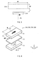
- Fig. 4 is an exploded perspective view showing the configuration of the element patterns 21A, 21B, 22A, and 22B.
- the ratio of dimensions does not coincide with the actual one.
- each of the element patterns 21A, 21B, 22A, and 22B has a spin valve structure in which a plurality of function films including magnetic layers are stacked, and includes a pinned layer 11 having a magnetization direction J11 pinned in the +X direction, a free layer 13 whose magnetization direction J13 changes according to external magnetic fields H such as the current magnetic field Hm1, and an intermediate layer 12 which is sandwiched between the pinned layer 11 and the free layer 13 and does not show any specific magnetization direction.
- the free layer 13 is made of a soft magnetic material such as nickel iron alloy (NiFe).
- the intermediate layer 12 is made of copper (Cu), whose top face is in contact with the pinned layer 11 and whose under face is in contact with the free layer 13.
- the intermediate layer 12 can be made of a nonmagnetic metal having high conductivity such as gold (Au) in addition to copper.
- a nonmagnetic metal having high conductivity such as gold (Au) in addition to copper.
- Each of the top face of the pinned layer 11 (the face on the side opposite to the intermediate layer 12) and the under face of the free layer 13 (the face on the side opposite to the intermediate layer 12) is protected with a not-shown protection film.
- Exchange bias magnetic fields Hin in the magnetization direction J11 hereinbelow, simply called “exchange bias magnetic fields Hin" are generated between the pinned layer 11 and the free layer 13 and act each other via the intermediate layer 12.
- the strength of the exchange bias magnetic field Hin changes as the spin direction in the free layer 13 rotates according to the interval between the pinned layer 11 and the free layer 13 (that is, the thickness of the intermediate layer 12).
- Fig. 4 shows a configuration example of the case where the free layer 13, the intermediate layer 12, and the pinned layer 11 are stacked in order from the bottom
- the element patterns 21A, 21B, 22A and 22B are constructed so that a length ML in the X axis direction (longitudinal dimension) is in a range between 10 times and 200 times as large as the width MW (width dimension) in the Y axis direction.
- a preferable range of the length ML is, for example, from 20 ⁇ m to 100 ⁇ m.
- each of the element patterns 21A and 21B has a strip shape having the length ML whose dimension is larger than the width MW, so that magnetic shape anisotropy is displayed along the Y axis direction.
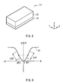
- Fig. 5 shows a detailed configuration of the pinned layer 11.
- the pinned layer 11 has a configuration in which a magnetization pinned film 14 and an antiferromagnetic film 15 are stacked in order from the side of the intermediate layer 12.
- the magnetization pinned film 14 is made of a ferromagnetic material such as cobalt (Co) or cobalt iron alloy (CoFe).
- the magnetization direction of the magnetization pinned film 14 is the magnetization direction J11 of the pinned layer 11 as a whole.
- the antiferromagnetic film 15 is made of an antiferromagnetic material such as platinum manganese alloy (PtMn) or iridium manganese alloy (IrMn).
- the antiferromagnetic film 15 is in the state where the spin magnetic moment in the +X direction and that in the opposite direction (-X direction) completely cancel out each other, and functions so as to pin the magnetization direction J11 of the magnetization pinned film 14.
- the magnetization direction J13 of the free layer 13 rotates by application of the current magnetic field Hm1, thereby changing a relative angle between the magnetization directions J13 and J11.
- the relative angle is determined according to the magnitude and the direction of the current magnetic field Hm1.
- Fig. 6 shows the relation between the external magnetic field H and the resistance change ratio ⁇ R/R when the external magnetic field H in the +Y direction is assumed to be positive.
- a bias magnetic field having a strength corresponding to a bias point BP1 (refer to Fig. 6) is preliminarily applied in the +Y direction to each of the element patterns 21A, 21B, 22A, and 22B in the MR elements 21 and 22.
- the current Im to be detected is supplied to the thin film coil 31 via the electrode films 41 and 42, and the current magnetic field Hm1 generated by the winding body portions 31A and 31B is detected by the element patterns 21A, 21B, 22A, and 22B.
- the current Im to be detected is passed from the end 31S toward the end 31E of the thin film coil 31, as shown in Fig.
- the current Im to be detected flows in the +X direction (from the back to this side in the diagram) in the winding body portions 31A and 31B.
- a current magnetic field Hm1 winding around each of the winding body portions 31A and 31B is generated according to the right-handed screw rule. Therefore, the current magnetic field Hm1 in the +Y direction is applied to each of the element patterns 21A and 21B, so that, as is evident from Fig. 6, the resistance change ratio increases (the resistance value increases).
- the current magnetic field Hm1 in the -Y direction is applied to the element patterns 22A and 22B, so that, as is obvious from Fig. 8, the resistance change ratio decreases (the resistance value decreases).
- Fig. 8 is an enlarged view of a part of Fig. 2, and an explanatory diagram for illustrating actions of the current magnetic fields Hm1 to the element patterns 21A, 21B, 22A, and 22B.
- Fig. 9 shows a circuit configuration of an ammeter including the current sensor 1A.
- a portion surrounded by a broken line corresponds to the current sensor 1A.
- the MR elements 21 and 22 and thin film coil 31 are disposed close to each another.
- each of the MR elements 21 and 22 is expressed as a single resistor obtained by connecting a plurality of element patterns in parallel.
- the MR elements 21 and 22 are coupled to each other at a first connection point P1 (the electrode pattern 7) and finally grounded via the electrode film 44.
- first connection point P1 the electrode pattern 7
- constant current sources 51 and 52 which are coupled to each other at a second connection point P2 are provided.
- an end on the side opposite to the first connection point P1 in the MR element 21 is connected to the constant current source 51 via the electrode film 43 as a third connection point P3.
- An end on the side opposite to the first connection point P1 in the MR element 22 is connected to the constant current source 52 via the electrode film 45 as a fourth connection point P4.
- the constant current sources 51 and 52 supply constant currents 10 whose values are equal to each other to the MR elements 21 and 22.
- the magnitude of the current magnetic field Hm1 can be obtained on the basis of a potential difference V0 between the third and fourth connection points P3 and P4 (the difference between voltage drops generated in the MR elements 21 and 22), and the magnitude of the current Im to be detected which generates the current magnetic field Hm1 having the same magnitude can be estimated. It will be concretely described hereinbelow.
- Equation (1) is calculated as follows.
- the MR elements 21 and 22 are disposed so that the resistance values R1 and R2 change in directions opposite to each other in accordance with the current magnetic field Hm1. Accordingly, the positive and negative signs of the change amounts ⁇ R1 and ⁇ R2 are opposite to each other. Therefore, in Equation (2), while the resistance values R1 and R2 before application of the current magnetic fields Hm1 cancel out each other, the change amounts ⁇ R1 and ⁇ R2 are maintained as they are.
- Equation (2) is calculated as follows.
- the MR elements 21 and 22 whose relation between an external magnetic field and a resistance change amount is grasped in advance, the magnitude of the current magnetic field Hm1 can be measured, and the magnitude of the current Im to be detected which generates the current magnetic field Hm1 of the same magnitude can be estimated.
- sensing is performed by using the two MR elements 21 and 22, so that the resistance change amount which is twice as large as that in the case of performing sensing using the MR element 21 or 22 singly can be obtained.
- the invention is advantageous with respect to higher precision of a measurement value.
- the MR elements 21 and 22 are provided in positions corresponding to the thin film coil 31 in the stacking direction. Consequently, as compared with the case where the thin film coil 31 and the MR elements 21 and 22 are provided so as to be adjacent to each other in an in-plane direction, they can be disposed closer to each other, so that the dimensions of the whole decrease. Further, the current magnetic field Hm1 based on the current Im to be detected flowing in the winding body portions 31A and 31B of the thin film coil 31 can be individually applied to each of the element patterns 21A, 21B, 22A, and 22B of the MR elements 21 and 22 by the winding body portions 31A and 31B of the thin film coil 31.
- the current magnetic field Hm1 can be efficiently applied to each of the element patterns 21A, 21B, 22A, and 22B. As a result, the current Im to be detected can be detected with high sensitivity.
- the element patterns 21A and 21B are connected in parallel to each other and the element patterns 22A and 22B are connected in parallel to each other, so that the resistance value of the whole first MR element 21 can be suppressed to be relatively low without decreasing the resistance change ratio, and a heating value at the time of use can be reduced. Moreover, the influence of noise from the outside (unnecessary magnetic fields) is reduced and the S/N ratio can be improved.
- the current magnetic field Hm1 can be detected by both of the MR elements 21 and 22. In this configuration, the resistance value R1 of the MR element 21 and the resistance value R2 of the MR element 22 change in directions opposite to each other.
- the current Im to be detected can be measured with high precision.
- the current sensor 1A can measure the current Im to be detected flowing in the thin film coil 31 with high precision while maintaining the compact configuration.
- Fig. 10 is a schematic view illustrating a perspective configuration of the current sensor 1B.
- Fig. 11 shows a sectional configuration taken along line XI-XI of the current sensor 1B illustrated in Fig. 10 seen from the direction indicated by the arrows (-X direction).
- the current sensor 1B is constructed by adding a second thin film coil 32 (hereinbelow, simply called the thin film coil 32), a third magnetoresistive element 23 (hereinbelow, simply called the MR element 23), and a fourth magnetoresistive element 24 (hereinbelow, simply called the MR element 24) to the current sensor 1A of the first embodiment.
- the MR element 23 is formed so as to be connected in series to the MR element 21 in a region at the first level L1 other than the region in which the MR element 21 is formed, and includes strip-shaped element patterns 23A and 23B which are provided so as to extend in the X axis direction and be adjacent to each other in the Y axis direction.
- the element patterns 23A and 23B are connected in parallel to each other between the electrode pattern 5 and an electrode pattern 8.
- the MR element 24 is formed so as to be connected in series to the MR element 22 in a region at the second level L2 other than the region in which the MR element 22 is formed, and includes strip-shaped element patterns 24A and 24B which are provided so as to extend in the X axis direction and be adjacent to each other in the Y axis direction.
- the element patterns 24A and 24B are connected in parallel to each other between the electrode pattern 7 and an electrode pattern 9.
- Each of the element patterns 23A and 23B and the element patterns 24A and 24B is formed so as to have a width such as 0.8 ⁇ m by sputtering or the like.
- the electrode pattern 4 is connected to the electrode pattern 6 and the electrode film 43 via a contact layer (not shown) and the electrode pattern 5 is connected to an electrode film 48 via a contact layer (not shown). Further, the electrode pattern 8 is connected to the electrode pattern 9 and an electrode film 47 via a contact layer (not shown) and the electrode pattern 7 is connected to the electrode film 44.
- the thin film coil 32 is a thin film pattern made of a metal material having high conductivity such as copper (Cu) in a manner similar to the thin film coil 31, and constructed so as to wind in a region at the third level L3 other than the region in which the thin film coil 31 is formed.
- the thin film coil 32 includes winding body portions 32A and 32B which extend in the X axis direction in correspondence with the element patterns 23A and 23B of the MR element 23 and the element patterns 24B and 24B of the MR element 24, respectively.
- the end 31E of the thin film coil 31 is connected to one end 32S of the thin film coil 32 via the electrode films 42 and 45, and the other end 32E of the thin film coil 32 is connected to an electrode film 46 via a contact layer (not shown). Therefore, the thin film coil 31 and 32 are formed as one conductor in the circuit configuration.
- the current Im to be detected passes through the thin film coil 31 and flows in the thin film coil 32, thereby applying, as shown in Fig. 12, the current magnetic field Hm1 to the element patterns 21A, 21B, 22A, and 22B and applying the current magnetic field Hm2 to the element patterns 23A, 23B, 24A, and 24B of the MR elements 23 and 24.
- Fig. 12 is an enlarged view of a part of Fig. 11 and an explanatory drawing for explaining action of the current magnetic field Hm1 on the element patterns 21A, 21B, 22A, and 22B and action of the current magnetic field Hm2 on the element patterns 23A, 23B, 24A, and 24B.
- the resistance values change according to the current magnetic field Hm1 applied.
- the resistance values 23A and 23B and the element patterns 24A and 24B change according to the current magnetic field Hm2.
- the resistance values of the element patterns 22A and 22B and the element patterns 23A and 23B change in the direction opposite to that of the resistance values of the element patterns 21A and 21B generated by the current magnetic field Hm1.
- the resistance values of the element patterns 24A and 24B change in the same direction as that of the resistance values of the element patterns 21A and 21B.
- a bias magnetic field having a strength corresponding to the bias point BP1 (refer to Fig. 6) is preliminarily applied to each of the element patterns 21A, 21B, 22A, and 22B in the +Y direction.
- the current Im to be detected is passed to the winding body portions 31A and 31B in the +X direction as shown in Fig. 12
- the current magnetic field Hm1 in the +Y direction is applied to the element patterns 21A and 22B. Therefore, as is the evident from Fig.6, the resistance change ratio increases (the resistance value increases).
- the resistance change ratio decreases (the resistance value decreases).
- the bias magnetic field having a strength corresponding to the bias point BP1 (refer to Fig. 6) in the +Y direction is preliminarily applied to each of the element patterns 23A, 23B, 24A, and 24B and the current Im to be detected in the -Y direction flows to the winding body portions 32A and 32B as shown in Fig. 12, the current magnetic field Hm2 in the -Y direction is applied to the element patterns 23A and 23B. Consequently, as is evident from Fig. 6, the resistance change ratio decreases (the resistance value decreases). On the other hand, the current magnetic field Hm2 in the +Y direction is applied to the element patterns 24A and 24B, so that, as is evident from Fig. 6, the resistance change ratio increases (the resistance value increases).
- Fig. 13 is a schematic view showing a circuit configuration of an ammeter including the current sensor 1B shown in Fig. 10.
- a portion surrounded by a broken line corresponds to the current sensor 1B.
- one end of the MR element 21 and one end of the MR element 22 are coupled to each other at the first connection point P1 and finally grounded via the electrode film 43.
- One end of the MR element 23 and one end of the MR element 24 are connected to each other at the second connection point P2.
- the end of the MR element 21 on the side opposite to the first connection point P1 and the end of the MR element 24 on the side opposite to the second connection point P2 are connected to each other at the electrode film 44 as the third connection point P3.
- a bridge circuit is constructed so that the current Im to be detected is detected on the basis of a potential difference V0 between the third and fourth connection points P3 and P4 when a voltage is applied across the first and second connection points P1 and P2.
- Fig. 14 is a simplified circuit diagram of a main part of Fig. 13.
- the resistance values of the MR elements 21 to 24 when a read current I0 flows in the state where the current magnetic fields Hm1 and Hm2 are not applied are expressed as R1 to R4, respectively.
- the read current I0 is diverted at the second connection point P2.
- a read current I1 passed through the MR elements 24 and 22 and a read current I2 passed through the MR elements 23 and 21 join at the first connection point P1.
- the potential difference V between the second and first connection points P2 and P1 can be expressed as follows.
- V 2 V ⁇ V 4
- V 0 ⁇ ( R 3 + ⁇ R 3 ) / ( R 3 + ⁇ R 3 + R 1 + ⁇ R 1 ) ⁇ ( R 4 + ⁇ R 4 ) / ( R 4 + ⁇ R 4 + R 2 + ⁇ R 2 ) ⁇ ⁇ V
- the resistance values R1 and R4 of the MR elements 21 and 24 change in the direction opposite to that of the resistance values R2 and R3 of the MR elements 22 and 23 (since the current magnetic fields Hm1 and Hm2 in the directions opposite to each other are applied to the MR elements 22 and 23 and to the MR elements 21 and 24, the bias magnetic field in the same direction is applied in advance to all of the MR elements 21 to 24). Consequently, the change amounts ⁇ R3 and ⁇ R1 cancel out each other and the change amounts ⁇ R4 and ⁇ R2 cancel out each other.
- the resistance values change (substantially, increase) only by the change amounts ⁇ R1 and ⁇ R4 ( ⁇ R1, ⁇ R4>0) in the MR elements 21 and 24.
- the resistance values change (substantially, decrease) only by the change amounts ⁇ R2 and ⁇ R3 ( ⁇ R2, ⁇ R3 ⁇ 0) in the MR elements 22 and 23.
- Equation (7) is calculated as follows.
- the magnitude of the current magnetic field Hm1 and Hm2 can be obtained, and the magnitude of the current Im to be detected that generates the current magnetic fields Hm1 and Hm2 can be estimated.
- the influence of variations in the characteristics in the MR elements is reduced, a larger resistance change amount in the element pattern of each of the MR elements can be detected, and precision of measurement values be can improved.
- the magnetization directions J11A to J11D of the pinned layers 11 in all of the MR elements 21 to 24 are set to be the same, so that the magnetization directions J11A to J11D form the same angle to the direction of the current magnetic field Hm.
- it is relatively easy to suppress variations in the detection sensitivity in the MR elements 21 to 24.
- the current sensor 1B of the embodiment has the configuration obtained by adding the thin film coil 32 coupled to the thin film coil 31, and the MR elements 23 and 24 corresponding to the thin film coil 32 to the configuration of the current sensor 1A of the first embodiment. Consequently, it is possible to construct a bridge circuit and perform sensing, and the precision of measurement values of the current Im to be detected can be further increased.
- the MR element 23 is provided at the same first level L1 as that of the MR element 21, and the MR element 24 is provided at the same second level L2 as that of the MR element 22. Therefore, the compact configuration can be maintained as a whole.
- the present invention has been described by the embodiments above, the invention is not limited to the foregoing embodiments but can be variously modified.
- the magnetoresistive element having the spin valve structure in which the magnetization direction of the pinned layer and the direction of the easy axis of magnetization of the free layer coincide with each other is employed in the embodiments, the invention is not limited to the configuration.
- a magnetoresistive element having a spin valve structure in which the magnetization direction of the pinned layer and the direction of the easy axis of magnetization of the free layer are orthogonal to each other may be used.
- each of the first to the fourth magnetoresistive elements is constructed by the two element patterns in the embodiments, the invention is not limited to the configuration, but each of the magnetoresistive elements may be constructed by three or more element patterns.
- the element patterns in the first to the fourth magnetoresistive elements are connected in parallel to each other in the embodiments, the element patterns may be connected in series as in a current sensor 1E as shown in Fig. 15.
- the total length of an element pattern functioning as a magnetosensitive part can be increased and the absolute value of the whole resistance value (impedance) in each of the first and second magnetoresistive elements can be increased. Therefore, even a weaker current to be detected can be measured with high precision.
- the current sensor of the invention is used to measure a current value itself as described in the foregoing embodiments and, further, can be also applied to an eddy current inspection technique for inspecting a defective in printed wiring and the like.
- a current sensor is constructed by arranging a number of magnetoresistive elements on a straight line and a change in an eddy current is grasped as a change in a magnetic flux.
Landscapes
- Physics & Mathematics (AREA)
- General Physics & Mathematics (AREA)
- Chemical & Material Sciences (AREA)
- Engineering & Computer Science (AREA)
- Nanotechnology (AREA)
- Condensed Matter Physics & Semiconductors (AREA)
- Crystallography & Structural Chemistry (AREA)
- Measuring Instrument Details And Bridges, And Automatic Balancing Devices (AREA)
- Measuring Magnetic Variables (AREA)
- Hall/Mr Elements (AREA)
Abstract
Description
- The present invention relates to a small-sized current sensor capable of sensing a change in current flowing in a conductor with high sensitivity.
- Hitherto, to accurately detect a small signal current flowing in a circuit in a communication device, for example, a method of connecting resistors in series in the circuit and measuring a voltage drop in the resistors is used. In this case, however, a load different from that in a communication system is applied, and there is the possibility that an adverse influence is exerted on the communication system. Consequently, a method of indirectly measuring a signal current by detecting the gradient of a current magnetic field generated by the signal current (while maintaining an insulated state so that direct current does not flow) is used. Examples of such a method are a method of using a transformer in which coils are connected to each other and a method using a photocoupler.
- In the method of using the transformer, although a signal current which is an alternate current can be transmitted, a signal current which is a direct current cannot be transmitted. Moreover, a frequency band in which the signal current as the direct current can be transmitted is limited. At a frequency other than in the proper frequency band, an impedance of the transformer changes, so that it lacks linearity, and an adverse influence may be exerted on the communication device and the like. On the other hand, the photocoupler has excellent frequency characteristics, but it is difficult to reduce the size when the photocoupler is used. There is also a problem such that, in long terms, deterioration in a signal intensity caused by a change with time tends to occur.
- Consequently, a current sensor in which a giant magnetoresistive element (hereinbelow, GMR element) producing a giant magnetoresistive effect is disposed in the current magnetic field generated by the signal current to detect the gradient of the current magnetic field has been proposed (refer to, for example, U.S. Patent No. 5,621,377). A current sensor using such a GMR element has an excellent detection sensitivity and responsiveness and can obtain detection characteristics which are stable also against a temperature change.
- Recently, a current sensor capable of detecting a weaker current and having a more compact general configuration is being demanded. In a current sensor using a conventional GMR element, however, a GMR element is provided so as to be adjacent to a line to be measured in an in-plane direction, so that it is difficult to detect a weak current and it is disadvantageous from the viewpoint of miniaturization.
- The present invention has been achieved in consideration of such problems, and an object of the invention is to provide a current sensor capable of measuring a current to be detected with high precision while realizing a compact configuration.
- A current sensor of the present invention has the following components (A) to (C).
- (A) a first magnetoresistive element including a plurality of strip-shaped element patterns which extend in a first direction at a first level and are disposed so as to be adjacent to each other in a second direction orthogonal to the first direction.
- (B) a second magnetoresistive element including a plurality of strip-shaped element patterns extending in the first direction and disposed so as to be adjacent to each other in the second direction at a second level different from the first level.
- (C) a first thin film coil which winds at a third level positioned between the first and second levels while including a plurality of winding body portions extending in the first direction in correspondence with the element patterns of the first and second magnetoresistive elements, and which applies a first current magnetic field to each of the element patterns of the first and second magnetoresistive elements when current to be detected is supplied.
- The strip shape denotes here a shape whose dimension in the first direction is larger than dimension in the second direction.
- In the current sensor according to the invention, as compared with the case where the first and second magnetoresistive elements and the first thin film coil are provided so as to be adjacent to each other in an in-plane direction, the first and second magnetoresistive elements are disposed more closely to the first thin film coil. Consequently, the dimensions of the whole are reduced and, moreover, a first current magnetic field based on the current to be detected which flows in the first thin film coil is applied to each of the element patterns of the first and second magnetoresistive elements more strongly. In this case, the first current magnetic field generated by the winding body portions of the first thin film coil corresponding to the element patterns of the first and second magnetoresistive elements is applied to each of the element patterns of the first and second magnetoresistive elements. Therefore, the positions and the sectional dimensions in a section orthogonal to the first direction are easily optimized from the viewpoint of heating by the coil and a current efficiency of coil magnetic field strength. As compared with the case where a current magnetic field generated only by a current flowing in one conductor (winding body portion) is applied to each of the element patterns, the first current magnetic field can be efficiently applied to each of the element patterns.
- Preferably, the current sensor of the invention is constructed so that the resistance values of the first and second magnetoresistive elements change in directions opposite to each other in accordance with the first current magnetic field.
- Preferably, the current sensor of the invention further includes: a third magnetoresistive element which includes a plurality of strip-shaped element patterns extending in the first direction and disposed so as to be adjacent to each other in the second direction, and which is formed in a region other than a region where the first magnetoresistive element at the first level is formed so as to be connected in series to the first magnetoresistive element; a fourth magnetoresistive element which includes a plurality of strip-shaped element patterns extending in the first direction and disposed so as to be adjacent to each other in the second direction and which is formed in a region other than a region where the second magnetoresistive element at the second level is formed so as to be connected in series to the second magnetoresistive element; and a second thin film coil which winds in a region other than a region where the first thin film coil at the third level is formed so as to include a plurality of winding body portions extending in the first direction in correspondence with the element patterns of the third and fourth magnetoresistive elements, and which applies a second current magnetic field to each of the element patterns of the third and fourth magnetoresistive elements when the current to be detected is supplied.
- In the above case, preferably, a resistance value of the second magnetoresistive element changes in the direction opposite to that of the first magnetoresistive element in accordance with the first current magnetic field, a resistance value of the third magnetoresistive element changes in the direction opposite to that of the first magnetoresistive element generated by the first current magnetic field in accordance with the second current magnetic field, and a resistance value of the fourth magnetoresistive element changes in the same direction as that of the first magnetoresistive element generated by the first current magnetic field in accordance with the second current magnetic field.
- Further in the above case, a bridge circuit may be constructed in such a manner that one end of the first magnetoresistive element and one end of the second magnetoresistive element are connected to each other at a first connection point, one end of the third magnetoresistive element and one end of the fourth magnetoresistive element are connected to each other at a second connection point, further, the other end of the first magnetoresistive element and the other end of the fourth magnetoresistive element are connected to each other at a third connection point, and the other end of the second magnetoresistive element and the other end of the third magnetoresistive element are connected to each other at a fourth connection point and, on the basis of a potential difference between the third and fourth connection points occurring when a voltage is applied across the first and second connection points, the current to be detected is detected.
- In the current sensor of the invention, the element patterns in each of the first to fourth magnetoresistive elements may be connected in parallel to each other or in series to each other.
- In the current sensor of the invention, preferably, each of the element patterns in the first to fourth magnetoresistive elements has a magnetization pinned film magnetized in the first direction. Further, it is preferable that each of the element patterns in the first to fourth magnetoresistive elements be constructed so that the longitudinal dimension along the first direction is 10 times to 200 times as large as the width dimension along the second direction. In this case, the width dimension along the second direction is preferably in a range from 0.5 µm to 2.0 µm. Further, it is preferable that each of the winding body portions in the first and second thin film coils have a section area which is from 0.4 µm2 to 2.0 µm2 in a cross section orthogonal to the first direction. In this case, for example, the winding body portion has a width dimension in a range from 0.8 µm to 3.0 µm and a thickness dimension in a range from 0.2 µm to 1.4 µm.
- According to the invention, the current sensor includes: first and second magnetoresistive elements including a plurality of strip-shaped element patterns extending at the first and second levels, respectively; and a first thin film coil which winds at a third level while including a plurality of winding body portions corresponding to the element patterns of the first and second magnetoresistive elements, and which applies a first current magnetic field to each of the element patterns of the first and second magnetoresistive elements when a current to be detected is supplied. Thus, while realizing a compact configuration, the current to be detected that flows in the first thin film coil can be measured with high sensitivity and high precision by using both of the first and second magnetoresistive elements.
- In the case, particularly, when the element patterns in the first magnetoresistive element are connected in parallel to each other, the resistance value as a whole can be suppressed to be relatively low without decreasing the resistance change ratio in the first magnetoresistive element, and a heating value of the first magnetoresistive element at the time of use can be reduced. Moreover, the influence of noise from the outside (unnecessary magnetic fields) is reduced, and the S/N ratio can be improved. On the other hand, when the element patterns are connected in series to each other, without increasing the dimension in the first direction, the total length of the element patterns functioning as magnetosensitive parts can be increased, and the absolute value of the resistance value (impedance) of the whole in the first magnetoresistive element can be made larger. Therefore, even a weaker current to be detected can be measured with high precision.
- When the current sensor of the invention includes, in addition to the first and second magnetoresistive elements and the first thin film coil, the third magnetoresistive element formed at the first level so as to be connected in series to the first magnetoresistive element, the fourth magnetoresistive element formed at the second level so as to be connected in series to the second magnetoresistive element, and the second thin film coil for applying the current magnetic field to each of the element patterns of the third and fourth magnetoresistive elements, the current to be detected is measured by using the four magnetoresistive elements. Consequently, the reliability of a measurement values of the current to be detected is improved more than the case of using two magnetoresistive elements. In this case, if a bridge circuit is constructed by using first to fourth magnetoresistive elements, the influence of variations in the characteristics among the magnetoresistive elements is reduced. Accordingly, the precision of the measurement can be further increased.
-
- Fig. 1 is a perspective view showing the configuration of a current sensor according to a first embodiment of the invention.
- Fig. 2 is a cross section taken along line II-II of the current sensor illustrated in Fig. 1.
- Fig. 3 is an enlarged cross section of a main part of Fig. 2.
- Fig. 4 is an exploded perspective view showing the configuration of a magnetoresistive element as a main part of the current sensor illustrated in Fig. 1.
- Fig. 5 is a perspective view showing the configuration of a part of the magnetoresistive element illustrated in Fig. 4.
- Fig. 6 is a characteristic diagram showing a magnetic field dependency of a resistance change ratio in the magnetoresistive element illustrated in Fig. 4.
- Fig. 7 is another exploded perspective view showing the configuration of the magnetoresistive element as a main part of the current sensor illustrated in Fig. 1.
- Fig. 8 is another enlarged cross section of a main part of Fig. 2.
- Fig. 9 is a circuit diagram corresponding to the current sensor shown in Fig. 1.
- Fig. 10 is a perspective view showing the configuration of a current sensor according to a second embodiment of the invention.
- Fig. 11 is a cross section taken along line XI-XI of the current sensor illustrated in Fig. 10.
- Fig. 12 is an enlarged cross section of a main part of Fig. 11.
- Fig. 13 is a circuit diagram corresponding to the current sensor shown in Fig. 10.
- Fig. 14 is an enlarged view of a main part of the circuit diagram of Fig. 13.
- Fig. 15 is a perspective view showing the configuration of a modification of the current sensor illustrated in Fig. 10.
- Embodiments of the invention will be described in detail hereinbelow with reference to the drawings
- First, the configuration of a current sensor as a first embodiment of the invention will be described with reference to Figs. 1 and 2. Fig. 1 is a schematic view illustrating a perspective configuration of a
current sensor 1 of the first embodiment. Fig. 2 is a cross section taken along line II-II of thecurrent sensor 1 illustrated in Fig. 1 seen from the direction indicated by the arrows (-X direction). Thecurrent sensor 1 is mounted on, for example, a communication device and is used for accurately measuring a current as a control signal. To distinguish the current sensor of the first embodiment from that of a second embodiment to be described later and the like, the current sensor in the first embodiment will be called acurrent sensor 1A. - The
current sensor 1A has a configuration obtained by sequentially stacking, on asubstrate 2 made of silicon (Si) or the like via abase film 3 made of aluminum oxide (Al2O3) or the like, a first level L1 including a first magnetoresistive element 21 (hereinbelow, simply called the MR element 21), a third level L3 including a first thin film coil 31(hereinbelow, simply called the thin film coil 31), and a second level L2 including a second magnetoresistive element 22 (hereinbelow, simply called the MR element 22). Concretely, theMR element 21 has twoelement patterns MR element 22 has twoelement patterns thin film coil 31 winds at the third level L3 while including a windingbody portion 31A extending in the X axis direction in correspondence with each of theelement patterns body portion 31B extending in the X axis direction in correspondence with each of theelement patterns - In the cross section of Fig. 2, the
MR element 21, thethin film coil 31, and theMR element 22 are covered with insulating films Z1 to Z3 made of Al2O3 or the like, respectively, and electrically insulated from each other. Moreover, a plurality ofelectrode films 41 to 44 (shown in Fig. 1) are provided on the insulating film Z3. - The
thin film coil 31 is a thin film pattern made of a metal material having high conductivity such as copper (Cu), and to which a current Im to be detected such as a control signal or the like is supplied. In thethin film coil 31, oneend 31S is connected to theelectrode film 41 via a contact layer (not shown) and theother end 31E is connected to theelectrode film 42 via a contact layer (not shown)(refer to Fig. 1). Thecurrent sensor 1A is set so that the current Im to be detected flows from theend 31S to theend 31E. - The
element patterns element patterns body portions thin film coil 31 in the stacking direction, respectively. Theelement patterns electrode patterns element patterns electrode patterns element patterns element patterns electrode pattern 4 is connected to theelectrode film 43 via a contact layer (not shown) and theelectrode pattern 5 is connected together with theelectrode pattern 7 via a contact layer (not shown) to theelectrode film 44. Theelectrode pattern 6 is connected to anelectrode film 45. - The
element patterns element patterns element patterns element patterns - Fig. 3 is an enlarged cross section of a main part of Fig. 2 and representatively shows the winding
body portion 31A andelement pattern 21A. The windingbody portion 31A andelement pattern 21A are disposed so that their center positions in the Y axis direction coincide with each other (that is, their center positions exist on a virtual center line CL extending in the X axis direction) and so as to be separated from each other by a distance D in the Y axis direction. The distance D is preferably 0.2 µm or more from the viewpoint of insulation resistance. Specifically, when the thickness of the insulating film Z1 by which the windingbody portion 31A and theelement pattern 21A are separated is 0.2 µm or more, the windingbody portion 31A and theelement pattern 21A can withstand instant application of 700V. From the viewpoint of realization of compactness, the distance D is preferably as small as possible. Concretely, the thickness D is preferably 1.0 µm or less. - The range of a section area S in a YZ cross section (cross section orthogonal to the X axis direction) of the winding
body portion 31A is preferably from 0.4 µm2 to 2.0 µm2. When the cross section area S is less than 0.4 µm2, there is the possibility that excessive temperature rise (for example, exceeding 1.0 °C) occurs due to the current Im to be detected flowing in the windingbody portion 31A (since thecurrent sensor 1A of the embodiment detects a control signal of a communication device or the like, the magnitude of the current Im to be detected lies in a range from 2 mA to 50 mA) and detection precision deteriorates. On the other hand, when the cross section area S exceeds 2.0µm2, the strength of the current magnetic fields Hm1 decreases and it becomes difficult to stably perform detecting operation by theelement pattern 21A. - The winding
body portion 31A having such a cross section area S is constructed to have, for example, a width MX in a range from 0.8 µm to 3.0 µm and a thickness MY in a range from 0.2 µm to 1.4 µm in the YZ cross section orthogonal to the X axis direction. A width MW of theelement pattern 21A in the Y axis direction is preferably 2.0 µm or less so that the current magnetic field Hm1 which is sufficiently uniform in the whole Y axis direction is applied to theelement pattern 21A. On the other hand, the lower limit of the width MW is preferably 0.5 µm in order to form a uniform film in the Y axis direction. Although only the relation between the windingbody portion 31A andelement pattern 21A is shown in Fig. 3, preferably, the relation between the windingbody portion 31A andelement pattern 22A is the same. Moreover, the relation between the windingbody portion 31B and each of theelement patterns - Next, the configuration of the
element patterns element patterns - As shown in Fig. 4, each of the
element patterns layer 11 having a magnetization direction J11 pinned in the +X direction, afree layer 13 whose magnetization direction J13 changes according to external magnetic fields H such as the current magnetic field Hm1, and anintermediate layer 12 which is sandwiched between the pinnedlayer 11 and thefree layer 13 and does not show any specific magnetization direction. Thefree layer 13 is made of a soft magnetic material such as nickel iron alloy (NiFe). Theintermediate layer 12 is made of copper (Cu), whose top face is in contact with the pinnedlayer 11 and whose under face is in contact with thefree layer 13. Theintermediate layer 12 can be made of a nonmagnetic metal having high conductivity such as gold (Au) in addition to copper. Each of the top face of the pinned layer 11 (the face on the side opposite to the intermediate layer 12) and the under face of the free layer 13 (the face on the side opposite to the intermediate layer 12) is protected with a not-shown protection film. Exchange bias magnetic fields Hin in the magnetization direction J11 (hereinbelow, simply called "exchange bias magnetic fields Hin") are generated between the pinnedlayer 11 and thefree layer 13 and act each other via theintermediate layer 12. The strength of the exchange bias magnetic field Hin changes as the spin direction in thefree layer 13 rotates according to the interval between the pinnedlayer 11 and the free layer 13 (that is, the thickness of the intermediate layer 12). Although Fig. 4 shows a configuration example of the case where thefree layer 13, theintermediate layer 12, and the pinnedlayer 11 are stacked in order from the bottom, the invention is not limited to the configuration. The layers may be stacked in the opposite order. - The
element patterns element patterns - Fig. 5 shows a detailed configuration of the pinned
layer 11. The pinnedlayer 11 has a configuration in which a magnetization pinned film 14 and anantiferromagnetic film 15 are stacked in order from the side of theintermediate layer 12. The magnetization pinned film 14 is made of a ferromagnetic material such as cobalt (Co) or cobalt iron alloy (CoFe). The magnetization direction of the magnetization pinned film 14 is the magnetization direction J11 of the pinnedlayer 11 as a whole. Theantiferromagnetic film 15 is made of an antiferromagnetic material such as platinum manganese alloy (PtMn) or iridium manganese alloy (IrMn). Theantiferromagnetic film 15 is in the state where the spin magnetic moment in the +X direction and that in the opposite direction (-X direction) completely cancel out each other, and functions so as to pin the magnetization direction J11 of the magnetization pinned film 14. - In the
element patterns free layer 13 rotates by application of the current magnetic field Hm1, thereby changing a relative angle between the magnetization directions J13 and J11. The relative angle is determined according to the magnitude and the direction of the current magnetic field Hm1. - Fig. 4 shows a no load state where the current magnetic field Hm1 is zero (Hm = 0) and the other magnetic fields (such as the bias magnetic field) are not applied (that is, the state where the external magnetic field H is zero). Since an easy magnetization axis direction AE13 of the
free layer 13 is set so as to be parallel with the magnetization direction J11 of the pinnedlayer 11, all of the easy magnetization axis direction AE13 and the magnetization directions J13 and J11 are parallel with each other along the +X direction in this state. Consequently, the spin directions of magnetic domains in thefree layer 13 align in almost the same direction. In the case where the external magnetic field H is applied to theelement patterns - As is evident from Fig. 6, however, a linear change cannot be obtained in a range around zero of the external magnetic field H (H=0). Therefore, in the case of actually measuring the current magnetic field Hm1, by applying a bias magnetic field generated by a not-shown permanent magnet or the like in a direction orthogonal to the magnetization direction J11, as shown in Fig. 7, the magnetization direction J13 is turned to be slightly tilted so as to include a component in the +Y direction or a component in the -Y direction (Fig. 7 shows the case where the magnetization direction J13 is tilted to the -Y direction). In such a manner, a change in the current magnetic field Hm1 can be detected with high precision in linear areas LA1 and LA2 having bias points BP1 and BP2 as center points, respectively, shown in Fig. 6.
- A method of sensing the current Im to be detected by the
current sensor 1A having the configuration as described above will be described hereinbelow with reference to Figs. 8 and 9 in addition to Figs. 1 to 7. - In the case of performing sensing by using the
current sensor 1A, for example, a bias magnetic field having a strength corresponding to a bias point BP1 (refer to Fig. 6) is preliminarily applied in the +Y direction to each of theelement patterns MR elements thin film coil 31 via theelectrode films body portions element patterns end 31S toward theend 31E of thethin film coil 31, as shown in Fig. 8, the current Im to be detected flows in the +X direction (from the back to this side in the diagram) in the windingbody portions body portions element patterns element patterns body portions body portions MR elements element patterns element patterns - Fig. 9 shows a circuit configuration of an ammeter including the
current sensor 1A. In Fig. 9, a portion surrounded by a broken line corresponds to thecurrent sensor 1A. As shown in Fig. 9, in thecurrent sensor 1A, theMR elements thin film coil 31 are disposed close to each another. In this configuration, each of theMR elements MR elements electrode film 44. On the side opposite to the first connection point P1 of theMR elements current sources MR element 21 is connected to the constantcurrent source 51 via theelectrode film 43 as a third connection point P3. An end on the side opposite to the first connection point P1 in theMR element 22 is connected to the constantcurrent source 52 via theelectrode film 45 as a fourth connection point P4. The constantcurrent sources MR elements - In the
current sensor 1A having such a configuration, when a voltage is applied across the first and second connection points P1 and P2, the magnitude of the current magnetic field Hm1 can be obtained on the basis of a potential difference V0 between the third and fourth connection points P3 and P4 (the difference between voltage drops generated in theMR elements 21 and 22), and the magnitude of the current Im to be detected which generates the current magnetic field Hm1 having the same magnitude can be estimated. It will be concretely described hereinbelow. - In Fig. 9, constant currents from the
constant sources whole MR elements 


- In this circuit, by measuring the potential difference V0 when the current magnetic field Hm1 is applied, the resistance change amount in each of the
MR elements 
- As already described above, the
MR elements - When it is assumed that the
MR elements
R1=R2=R and
Δ R1 = -ΔR2 = ΔR, - Equation (2) is calculated as follows.

- Therefore, by using the
MR elements MR elements MR element - According to the
current sensor 1A of the embodiment as described above, theMR elements thin film coil 31 in the stacking direction. Consequently, as compared with the case where thethin film coil 31 and theMR elements body portions thin film coil 31 can be individually applied to each of theelement patterns MR elements body portions thin film coil 31. Therefore, optimization of the dispose positions and cross section dimensions in the cross section orthogonal to the first direction can be easily realized from the viewpoint of heating by the coil and current efficiency of coil magnetic field strength. As compared with the case where a current magnetic field generated only by a current flowing in one conductor (winding body portion) is applied to each of element patterns, the current magnetic field Hm1 can be efficiently applied to each of theelement patterns - In particular, the
element patterns element patterns first MR element 21 can be suppressed to be relatively low without decreasing the resistance change ratio, and a heating value at the time of use can be reduced. Moreover, the influence of noise from the outside (unnecessary magnetic fields) is reduced and the S/N ratio can be improved. In addition, the current magnetic field Hm1 can be detected by both of theMR elements MR element 21 and the resistance value R2 of theMR element 22 change in directions opposite to each other. Consequently, on the basis of the difference V0 between voltage drops that occur when the constant currents I0 which are equal to each other are passed to theMR elements current sensor 1A can measure the current Im to be detected flowing in thethin film coil 31 with high precision while maintaining the compact configuration. - Next, a
current sensor 1B as a second embodiment of the invention will be described with reference to Figs. 10 and 11. - Fig. 10 is a schematic view illustrating a perspective configuration of the
current sensor 1B. Fig. 11 shows a sectional configuration taken along line XI-XI of thecurrent sensor 1B illustrated in Fig. 10 seen from the direction indicated by the arrows (-X direction). Thecurrent sensor 1B is constructed by adding a second thin film coil 32 (hereinbelow, simply called the thin film coil 32), a third magnetoresistive element 23 (hereinbelow, simply called the MR element 23), and a fourth magnetoresistive element 24 (hereinbelow, simply called the MR element 24) to thecurrent sensor 1A of the first embodiment. - The
MR element 23 is formed so as to be connected in series to theMR element 21 in a region at the first level L1 other than the region in which theMR element 21 is formed, and includes strip-shapedelement patterns element patterns electrode pattern 5 and anelectrode pattern 8. TheMR element 24 is formed so as to be connected in series to theMR element 22 in a region at the second level L2 other than the region in which theMR element 22 is formed, and includes strip-shapedelement patterns element patterns electrode pattern 7 and an electrode pattern 9. Each of theelement patterns element patterns electrode pattern 4 is connected to theelectrode pattern 6 and theelectrode film 43 via a contact layer (not shown) and theelectrode pattern 5 is connected to anelectrode film 48 via a contact layer (not shown). Further, theelectrode pattern 8 is connected to the electrode pattern 9 and anelectrode film 47 via a contact layer (not shown) and theelectrode pattern 7 is connected to theelectrode film 44. - Further, the
thin film coil 32 is a thin film pattern made of a metal material having high conductivity such as copper (Cu) in a manner similar to thethin film coil 31, and constructed so as to wind in a region at the third level L3 other than the region in which thethin film coil 31 is formed. Thethin film coil 32 includes windingbody portions element patterns MR element 23 and theelement patterns MR element 24, respectively. Theend 31E of thethin film coil 31 is connected to oneend 32S of thethin film coil 32 via theelectrode films other end 32E of thethin film coil 32 is connected to anelectrode film 46 via a contact layer (not shown). Therefore, thethin film coil - In the current sensor1B having such a configuration, the current Im to be detected passes through the
thin film coil 31 and flows in thethin film coil 32, thereby applying, as shown in Fig. 12, the current magnetic field Hm1 to theelement patterns element patterns MR elements element patterns element patterns element patterns element patterns element patterns element patterns element patterns element patterns element patterns element patterns element patterns - For example, a bias magnetic field having a strength corresponding to the bias point BP1 (refer to Fig. 6) is preliminarily applied to each of the
element patterns body portions element patterns element patterns element patterns body portions element patterns element patterns - Fig. 13 is a schematic view showing a circuit configuration of an ammeter including the
current sensor 1B shown in Fig. 10. In Fig. 13, a portion surrounded by a broken line corresponds to thecurrent sensor 1B. As shown in Fig. 13, one end of theMR element 21 and one end of theMR element 22 are coupled to each other at the first connection point P1 and finally grounded via theelectrode film 43. One end of theMR element 23 and one end of theMR element 24 are connected to each other at the second connection point P2. Further, the end of theMR element 21 on the side opposite to the first connection point P1 and the end of theMR element 24 on the side opposite to the second connection point P2 are connected to each other at theelectrode film 44 as the third connection point P3. The end of theMR element 22 on the side opposite to the first connection point P1 and the end of theMR element 23 on the side opposite to the second connection point P2 are connected to each other at theelectrode 48 as the fourth connection point P4. In such a manner, a bridge circuit is constructed so that the current Im to be detected is detected on the basis of a potential difference V0 between the third and fourth connection points P3 and P4 when a voltage is applied across the first and second connection points P1 and P2. - A method of measuring the current magnetic fields Hm1 and Hm2 generated by the current Im to be detected will be described hereinbelow by referring to Fig. 14 in addition to Fig. 13. Fig. 14 is a simplified circuit diagram of a main part of Fig. 13.
- In Fig. 14, the resistance values of the
MR elements 21 to 24 when a read current I0 flows in the state where the current magnetic fields Hm1 and Hm2 are not applied are expressed as R1 to R4, respectively. The read current I0 is diverted at the second connection point P2. After that, a read current I1 passed through theMR elements MR elements 
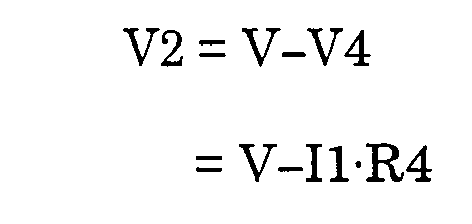

- Therefore, the potential difference V0 between the third and fourth connection, points P3 and P4 is expressed as follows.

- From Equation (4), the following is derived.

- In the bridge circuit, when the current magnetic fields Hm1 and Hm2 are applied, by measuring the potential V0 between the third and fourth connection points P3 and P4 expressed by the equation (6), the resistance change amount is obtained. It is assumed that when the current magnetic fields Hm1 and Hm2 are applied, the resistance values R1 to R4 increase only by change amounts ΔR1 to ΔR4, respectively, that is, the resistance values R1 to R4 change as follows.


- After applying the current magnetic fields Hm1 and Hm2, from Equation (6), the following is obtained.

- As already described above, in the
current sensor 1B, the resistance values R1 and R4 of theMR elements MR elements 22 and 23 (since the current magnetic fields Hm1 and Hm2 in the directions opposite to each other are applied to theMR elements MR elements MR elements 21 to 24). Consequently, the change amounts ΔR3 and ΔR1 cancel out each other and the change amounts ΔR4 and ΔR2 cancel out each other. Therefore, when the states of both before and after application of the current magnetic fields Hm1 and Hm2 are compared to each other, the denominator in each of terms of equation (7) hardly increases. On the other hand, since the change amounts ΔR3 and ΔR4 always have signs opposite to each other, they cancel out each other and a numerator of each of the terms increases/decreases for the following reason. As is evident from Fig. 6, when the current magnetic fields Hm1 and Hm2 in the +Y direction are applied in the state where the bias magnetic field corresponding to the bias point BP1 is preliminarily applied, the resistance values change (substantially, increase) only by the change amounts ΔR1 and ΔR4 (ΔR1, ΔR4>0) in theMR elements MR elements - When it is assumed that the
MR elements 21 to 24 have the same characteristics, that is,
R = R1 = R2 = R3 = R4 and
Δ R1 = -ΔR1 = ΔR2 = ΔR3 = -ΔR4, - Equation (7) is calculated as follows.

- As described above, by using the
MR elements 21 to 22 whose characteristic values such as the resistance change ratio ΔR/R are grasped in advance, the magnitude of the current magnetic field Hm1 and Hm2 can be obtained, and the magnitude of the current Im to be detected that generates the current magnetic fields Hm1 and Hm2 can be estimated. In particular, by constructing a bridge circuit and performing sensing, as compared with sensing performed by a single element pattern having equivalent output, the influence of variations in the characteristics in the MR elements is reduced, a larger resistance change amount in the element pattern of each of the MR elements can be detected, and precision of measurement values be can improved. In the embodiment, the magnetization directions J11A to J11D of the pinned layers 11 in all of theMR elements 21 to 24 are set to be the same, so that the magnetization directions J11A to J11D form the same angle to the direction of the current magnetic field Hm. Thus, it is relatively easy to suppress variations in the detection sensitivity in theMR elements 21 to 24. - As described above, the
current sensor 1B of the embodiment has the configuration obtained by adding thethin film coil 32 coupled to thethin film coil 31, and theMR elements thin film coil 32 to the configuration of thecurrent sensor 1A of the first embodiment. Consequently, it is possible to construct a bridge circuit and perform sensing, and the precision of measurement values of the current Im to be detected can be further increased. In this case, theMR element 23 is provided at the same first level L1 as that of theMR element 21, and theMR element 24 is provided at the same second level L2 as that of theMR element 22. Therefore, the compact configuration can be maintained as a whole. - Although the present invention has been described by the embodiments above, the invention is not limited to the foregoing embodiments but can be variously modified. For example, although the magnetoresistive element having the spin valve structure in which the magnetization direction of the pinned layer and the direction of the easy axis of magnetization of the free layer coincide with each other is employed in the embodiments, the invention is not limited to the configuration. For example, a magnetoresistive element having a spin valve structure in which the magnetization direction of the pinned layer and the direction of the easy axis of magnetization of the free layer are orthogonal to each other may be used.
- Although each of the first to the fourth magnetoresistive elements is constructed by the two element patterns in the embodiments, the invention is not limited to the configuration, but each of the magnetoresistive elements may be constructed by three or more element patterns.
- Further, although the element patterns in the first to the fourth magnetoresistive elements are connected in parallel to each other in the embodiments, the element patterns may be connected in series as in a current sensor 1E as shown in Fig. 15. In this case, without increasing the dimension in the first direction, the total length of an element pattern functioning as a magnetosensitive part can be increased and the absolute value of the whole resistance value (impedance) in each of the first and second magnetoresistive elements can be increased. Therefore, even a weaker current to be detected can be measured with high precision.
- The current sensor of the invention is used to measure a current value itself as described in the foregoing embodiments and, further, can be also applied to an eddy current inspection technique for inspecting a defective in printed wiring and the like. In an example of application, a current sensor is constructed by arranging a number of magnetoresistive elements on a straight line and a change in an eddy current is grasped as a change in a magnetic flux.
Claims (15)
- A current sensor comprising:a first magnetoresistive element which includes a plurality of strip-shaped element patterns extending in a first direction and disposed so as to be adjacent to each other in a second direction orthogonal to the first direction at a first level;a second magnetoresistive element which includes a plurality of strip-shaped element patterns extending in the first direction and disposed so as to be adjacent to each other in the second direction at a second level different from the first level; anda first thin film coil which winds at a third level positioned between the first and second levels while including a plurality of winding body portions extending in the first direction in correspondence with each of the element patterns of the first and second magnetoresistive elements, the first thin film coil applying a first current magnetic field to each of the element patterns of the first and second magnetoresistive elements when a current to be detected is supplied.
- A current sensor according to claim 1, wherein resistance values of the first and second magnetoresistive elements change in directions opposite to each other in accordance with the first current magnetic field.
- A current sensor according to claim 1, wherein each of the element patterns in the first and second magnetoresistive elements is connected in parallel to each other.
- A current sensor according to claim 1, wherein each of the element patterns of the first and second magnetoresistive elements is connected in series to each other.
- A current sensor according to claim 1, wherein each of the element patterns in the first and second magnetoresistive elements has a magnetization pinned film magnetized in the first direction.
- A current sensor according to claims 1, wherein each of the element patterns in the first and second magnetoresistive elements is constructed so that a longitudinal dimension along the first direction is 10 times to 200 times as large as a width dimension along the second direction.
- A current sensor according to claim 6, wherein the width dimension along the second direction is in a range from 0.5 µm to 2.0 µm.
- A current sensor according to claim 1, further comprising:a third magnetoresistive element which includes a plurality of strip-shaped element patterns extending in the first direction and disposed so as to be adjacent to each other in the second direction, and the third magnetoresistive element being formed at the first level in a region other than a region where the first magnetoresistive element is formed so as to be connected in series to the first magnetoresistive element;a fourth magnetoresistive element which includes a plurality of strip-shaped element patterns extending in the first direction and disposed so as to be adjacent to each other in the second direction, the fourth magnetoresistive element being formed in a region other than a region where the second magnetoresistive element at the second level is formed so as to be connected in series to the second magnetoresistive element; anda second thin film coil which winds in a region other than a region where the first thin film coil at the third level is formed so as to include a plurality of winding body portions extending in the first direction in correspondence with each of the element patterns of the third and fourth magnetoresistive elements, the second thin film coil applying a second current magnetic field to each of the element patterns of the third and fourth magnetoresistive elements when the current to be detected is supplied.
- A current sensor according to claim 8, wherein a resistance value of the second magnetoresistive element changes in the direction opposite to that of the first magnetoresistive element in accordance with the first current magnetic field,
a resistance value of the third magnetoresistive element changes in accordance with the second current magnetic field in the direction opposite to that of the first magnetoresistive element generated by the first current magnetic field, and
a resistance value of the fourth magnetoresistive element changes in accordance with the second current magnetic field in the same direction as that of the first magnetoresistive element generated by the first current magnetic field. - A current sensor according to claim 8, wherein the element patterns in each of the first to fourth magnetoresistive elements are connected in parallel to each other.
- A current sensor according to claim 8, wherein the element patterns in each of the first to fourth magnetoresistive elements are connected in series to each other.
- A current sensor according to claim 8, wherein each of the element patterns in the first to fourth magnetoresistive elements has a magnetization pinned film magnetized in the first direction.
- A current sensor according to claims 8, wherein a longitudinal dimension along the first direction of each of the element patterns in the first to fourth magnetoresistive elements is 10 times to 200 times as large as a width direction along the second direction.
- A current sensor according to claim 13, wherein the width dimension along the second direction is in a range from 0.5 µm to 2.0 µm.
- A current sensor according to claim 8, wherein a bridge circuit is constructed in such a manner that one end of the first magnetoresistive element and one end of the second magnetoresistive element are connected to each other at a first connection point,
one end of the third magnetoresistive element and one end of the fourth magnetoresistive element are connected to each other at a second connection point,
the other end of the first magnetoresistive element and the other end of the fourth magnetoresistive element are connected to each other at a third connection point, and
the other end of the second magnetoresistive element and the other end of the third magnetoresistive element are connected to each other at a fourth connection point, and
on the basis of a potential difference between the third and fourth connection points occurring when a voltage is applied across the first and second connection points, the current to be detected is detected.
Applications Claiming Priority (1)
| Application Number | Priority Date | Filing Date | Title |
|---|---|---|---|
| JP2004352212A JP4105147B2 (en) | 2004-12-06 | 2004-12-06 | Current sensor |
Publications (1)
| Publication Number | Publication Date |
|---|---|
| EP1666894A1 true EP1666894A1 (en) | 2006-06-07 |
Family
ID=35788053
Family Applications (1)
| Application Number | Title | Priority Date | Filing Date |
|---|---|---|---|
| EP05025790A Withdrawn EP1666894A1 (en) | 2004-12-06 | 2005-11-25 | Current sensor |
Country Status (3)
| Country | Link |
|---|---|
| US (1) | US7504927B2 (en) |
| EP (1) | EP1666894A1 (en) |
| JP (1) | JP4105147B2 (en) |
Cited By (10)
| Publication number | Priority date | Publication date | Assignee | Title |
|---|---|---|---|---|
| US8728825B2 (en) | 2006-08-01 | 2014-05-20 | Headway Technologies, Inc. | GMR sensor stripe for a biosensor with enhanced sensitivity |
| EP2848948A4 (en) * | 2012-05-11 | 2016-06-01 | Univ Osaka City | DEVICE FOR MEASURING A POWER FACTOR |
| US9529060B2 (en) | 2014-01-09 | 2016-12-27 | Allegro Microsystems, Llc | Magnetoresistance element with improved response to magnetic fields |
| US9812637B2 (en) | 2015-06-05 | 2017-11-07 | Allegro Microsystems, Llc | Spin valve magnetoresistance element with improved response to magnetic fields |
| US10620279B2 (en) | 2017-05-19 | 2020-04-14 | Allegro Microsystems, Llc | Magnetoresistance element with increased operational range |
| US11022661B2 (en) | 2017-05-19 | 2021-06-01 | Allegro Microsystems, Llc | Magnetoresistance element with increased operational range |
| US11719771B1 (en) | 2022-06-02 | 2023-08-08 | Allegro Microsystems, Llc | Magnetoresistive sensor having seed layer hysteresis suppression |
| US12320870B2 (en) | 2022-07-19 | 2025-06-03 | Allegro Microsystems, Llc | Controlling out-of-plane anisotropy in an MR sensor with free layer dusting |
| US12352832B2 (en) | 2023-01-30 | 2025-07-08 | Allegro Microsystems, Llc | Reducing angle error in angle sensor due to orthogonality drift over magnetic-field |
| US12359904B2 (en) | 2023-01-26 | 2025-07-15 | Allegro Microsystems, Llc | Method of manufacturing angle sensors including magnetoresistance elements including different types of antiferromagnetic materials |
Families Citing this family (45)
| Publication number | Priority date | Publication date | Assignee | Title |
|---|---|---|---|---|
| US7259545B2 (en) | 2003-02-11 | 2007-08-21 | Allegro Microsystems, Inc. | Integrated sensor |
| US7476816B2 (en) * | 2003-08-26 | 2009-01-13 | Allegro Microsystems, Inc. | Current sensor |
| US20060219436A1 (en) * | 2003-08-26 | 2006-10-05 | Taylor William P | Current sensor |
| US7709754B2 (en) * | 2003-08-26 | 2010-05-04 | Allegro Microsystems, Inc. | Current sensor |
| US7777607B2 (en) * | 2004-10-12 | 2010-08-17 | Allegro Microsystems, Inc. | Resistor having a predetermined temperature coefficient |
| US7768083B2 (en) | 2006-01-20 | 2010-08-03 | Allegro Microsystems, Inc. | Arrangements for an integrated sensor |
| US20070279053A1 (en) * | 2006-05-12 | 2007-12-06 | Taylor William P | Integrated current sensor |
| JP4816952B2 (en) * | 2006-11-17 | 2011-11-16 | Tdk株式会社 | Current sensor |
| US7795862B2 (en) | 2007-10-22 | 2010-09-14 | Allegro Microsystems, Inc. | Matching of GMR sensors in a bridge |
| US8269491B2 (en) * | 2008-02-27 | 2012-09-18 | Allegro Microsystems, Inc. | DC offset removal for a magnetic field sensor |
| US8242776B2 (en) * | 2008-03-26 | 2012-08-14 | Everspin Technologies, Inc. | Magnetic sensor design for suppression of barkhausen noise |
| US7816905B2 (en) | 2008-06-02 | 2010-10-19 | Allegro Microsystems, Inc. | Arrangements for a current sensing circuit and integrated current sensor |
| US8093670B2 (en) * | 2008-07-24 | 2012-01-10 | Allegro Microsystems, Inc. | Methods and apparatus for integrated circuit having on chip capacitor with eddy current reductions |
| US8063634B2 (en) * | 2008-07-31 | 2011-11-22 | Allegro Microsystems, Inc. | Electronic circuit and method for resetting a magnetoresistance element |
| US7973527B2 (en) | 2008-07-31 | 2011-07-05 | Allegro Microsystems, Inc. | Electronic circuit configured to reset a magnetoresistance element |
| US20110133732A1 (en) * | 2009-12-03 | 2011-06-09 | Allegro Microsystems, Inc. | Methods and apparatus for enhanced frequency response of magnetic sensors |
| US8952686B2 (en) * | 2011-10-25 | 2015-02-10 | Honeywell International Inc. | High current range magnetoresistive-based current sensor |
| US8629539B2 (en) | 2012-01-16 | 2014-01-14 | Allegro Microsystems, Llc | Methods and apparatus for magnetic sensor having non-conductive die paddle |
| US9666788B2 (en) | 2012-03-20 | 2017-05-30 | Allegro Microsystems, Llc | Integrated circuit package having a split lead frame |
| US9812588B2 (en) | 2012-03-20 | 2017-11-07 | Allegro Microsystems, Llc | Magnetic field sensor integrated circuit with integral ferromagnetic material |
| US9494660B2 (en) | 2012-03-20 | 2016-11-15 | Allegro Microsystems, Llc | Integrated circuit package having a split lead frame |
| US10234513B2 (en) | 2012-03-20 | 2019-03-19 | Allegro Microsystems, Llc | Magnetic field sensor integrated circuit with integral ferromagnetic material |
| JP2015155796A (en) * | 2012-05-31 | 2015-08-27 | パナソニック株式会社 | Current sensor |
| US9190606B2 (en) | 2013-03-15 | 2015-11-17 | Allegro Micosystems, LLC | Packaging for an electronic device |
| US10345343B2 (en) | 2013-03-15 | 2019-07-09 | Allegro Microsystems, Llc | Current sensor isolation |
| US9964602B2 (en) * | 2013-03-18 | 2018-05-08 | Hitachi Metals, Ltd. | Magnetic sensor |
| US9411025B2 (en) | 2013-04-26 | 2016-08-09 | Allegro Microsystems, Llc | Integrated circuit package having a split lead frame and a magnet |
| US9354284B2 (en) | 2014-05-07 | 2016-05-31 | Allegro Microsystems, Llc | Magnetic field sensor configured to measure a magnetic field in a closed loop manner |
| US9322887B1 (en) | 2014-12-01 | 2016-04-26 | Allegro Microsystems, Llc | Magnetic field sensor with magnetoresistance elements and conductive-trace magnetic source |
| US9778288B2 (en) * | 2015-08-24 | 2017-10-03 | Texas Instruments Incorporated | Fluxgate-based current sensor |
| US10935612B2 (en) | 2018-08-20 | 2021-03-02 | Allegro Microsystems, Llc | Current sensor having multiple sensitivity ranges |
| US11009798B2 (en) * | 2018-09-05 | 2021-05-18 | Micron Technology, Inc. | Wafer alignment markers, systems, and related methods |
| US11251096B2 (en) | 2018-09-05 | 2022-02-15 | Micron Technology, Inc. | Wafer registration and overlay measurement systems and related methods |
| JP2020148640A (en) * | 2019-03-14 | 2020-09-17 | 株式会社東芝 | Current detector |
| US10991644B2 (en) | 2019-08-22 | 2021-04-27 | Allegro Microsystems, Llc | Integrated circuit package having a low profile |
| FR3101150B1 (en) * | 2019-09-19 | 2021-10-29 | Continental Automotive Gmbh | Automotive resistive sensor architecture |
| DE102020130296B4 (en) * | 2019-12-11 | 2025-06-05 | Tdk Corporation | MAGNETIC FIELD DETECTION DEVICE AND CURRENT METER |
| US11372029B2 (en) * | 2019-12-11 | 2022-06-28 | Tdk Corporation | Magnetic field detection apparatus and current detection apparatus |
| JP7341926B2 (en) | 2020-03-11 | 2023-09-11 | 株式会社東芝 | magnetic sensor |
| US11187764B2 (en) | 2020-03-20 | 2021-11-30 | Allegro Microsystems, Llc | Layout of magnetoresistance element |
| US11800813B2 (en) | 2020-05-29 | 2023-10-24 | Allegro Microsystems, Llc | High isolation current sensor |
| US11567108B2 (en) | 2021-03-31 | 2023-01-31 | Allegro Microsystems, Llc | Multi-gain channels for multi-range sensor |
| EP4130772B1 (en) | 2021-08-05 | 2025-07-23 | Allegro MicroSystems, LLC | Magnetoresistive element having compensated temperature coefficient of tmr |
| US11768230B1 (en) | 2022-03-30 | 2023-09-26 | Allegro Microsystems, Llc | Current sensor integrated circuit with a dual gauge lead frame |
| US12248039B2 (en) | 2023-08-08 | 2025-03-11 | Allegro Microsystems, Llc | Interleaving sub-arrays of magnetoresistance elements based on reference directions to compensate for bridge offset |
Citations (9)
| Publication number | Priority date | Publication date | Assignee | Title |
|---|---|---|---|---|
| US4464625A (en) * | 1980-12-24 | 1984-08-07 | Lgz Landis & Gyr Zug Ag. | Magnetoresistive current detector |
| CH660237A5 (en) * | 1982-04-08 | 1987-03-31 | Landis & Gyr Ag | Arrangement for detecting the zero crossing of a magnetic field |
| US5621377A (en) | 1993-01-13 | 1997-04-15 | Lust Electronic-Systeme Gmbh | Sensor assembly for measuring current as a function of magnetic field gradient |
| US5909115A (en) * | 1994-10-25 | 1999-06-01 | Sony Corporation | Position detecting apparatus employing magnetoresistance effect elements connected in series |
| US5933003A (en) * | 1994-09-26 | 1999-08-03 | Lust Antriebstechnik Gmbh | Magnetoresistive wheatstone bridge with compensating current conductor for measuring an electric current |
| US20030057938A1 (en) * | 2001-08-27 | 2003-03-27 | International Rectifier Corporation | Magnetoresistive magnetic field sensors and motor control devices using same |
| US6614211B1 (en) * | 1999-04-01 | 2003-09-02 | Santronics, Inc. | Non-contact detector for sensing a periodically varying magnetic field |
| US20040021544A1 (en) * | 2002-08-01 | 2004-02-05 | Honeywell International Inc. | Integrated magnetic signal isolator with feedback |
| WO2004072672A1 (en) * | 2003-02-11 | 2004-08-26 | Allegro Microsystems, Inc. | Integrated sensor |
Family Cites Families (2)
| Publication number | Priority date | Publication date | Assignee | Title |
|---|---|---|---|---|
| JP3206027B2 (en) | 1991-07-05 | 2001-09-04 | 株式会社村田製作所 | Micro current sensor |
| US5422571A (en) * | 1993-02-08 | 1995-06-06 | International Business Machines Corporation | Magnetoresistive spin valve sensor having a nonmagnetic back layer |
-
2004
- 2004-12-06 JP JP2004352212A patent/JP4105147B2/en not_active Expired - Lifetime
-
2005
- 2005-11-21 US US11/282,754 patent/US7504927B2/en active Active
- 2005-11-25 EP EP05025790A patent/EP1666894A1/en not_active Withdrawn
Patent Citations (9)
| Publication number | Priority date | Publication date | Assignee | Title |
|---|---|---|---|---|
| US4464625A (en) * | 1980-12-24 | 1984-08-07 | Lgz Landis & Gyr Zug Ag. | Magnetoresistive current detector |
| CH660237A5 (en) * | 1982-04-08 | 1987-03-31 | Landis & Gyr Ag | Arrangement for detecting the zero crossing of a magnetic field |
| US5621377A (en) | 1993-01-13 | 1997-04-15 | Lust Electronic-Systeme Gmbh | Sensor assembly for measuring current as a function of magnetic field gradient |
| US5933003A (en) * | 1994-09-26 | 1999-08-03 | Lust Antriebstechnik Gmbh | Magnetoresistive wheatstone bridge with compensating current conductor for measuring an electric current |
| US5909115A (en) * | 1994-10-25 | 1999-06-01 | Sony Corporation | Position detecting apparatus employing magnetoresistance effect elements connected in series |
| US6614211B1 (en) * | 1999-04-01 | 2003-09-02 | Santronics, Inc. | Non-contact detector for sensing a periodically varying magnetic field |
| US20030057938A1 (en) * | 2001-08-27 | 2003-03-27 | International Rectifier Corporation | Magnetoresistive magnetic field sensors and motor control devices using same |
| US20040021544A1 (en) * | 2002-08-01 | 2004-02-05 | Honeywell International Inc. | Integrated magnetic signal isolator with feedback |
| WO2004072672A1 (en) * | 2003-02-11 | 2004-08-26 | Allegro Microsystems, Inc. | Integrated sensor |
Cited By (18)
| Publication number | Priority date | Publication date | Assignee | Title |
|---|---|---|---|---|
| EP2390651B1 (en) * | 2006-08-01 | 2016-02-10 | MagIC Technologies Inc. | GMR biosensor with enhanced sensitivity |
| US9429544B2 (en) | 2006-08-01 | 2016-08-30 | Headway Technologies, Inc. | GMR biosensor with enhanced sensitivity |
| US8728825B2 (en) | 2006-08-01 | 2014-05-20 | Headway Technologies, Inc. | GMR sensor stripe for a biosensor with enhanced sensitivity |
| US10203379B2 (en) | 2006-08-01 | 2019-02-12 | Headway Technologies, Inc. | GMR biosensor with enhanced sensitivity |
| US10120001B2 (en) | 2012-05-11 | 2018-11-06 | Osaka City University | Power factor measurement device |
| EP2848948A4 (en) * | 2012-05-11 | 2016-06-01 | Univ Osaka City | DEVICE FOR MEASURING A POWER FACTOR |
| US9529060B2 (en) | 2014-01-09 | 2016-12-27 | Allegro Microsystems, Llc | Magnetoresistance element with improved response to magnetic fields |
| US9922673B2 (en) | 2014-01-09 | 2018-03-20 | Allegro Microsystems, Llc | Magnetoresistance element with improved response to magnetic fields |
| US9804234B2 (en) | 2014-01-09 | 2017-10-31 | Allegro Microsystems, Llc | Magnetoresistance element with an improved seed layer to promote an improved response to magnetic fields |
| US10347277B2 (en) | 2014-01-09 | 2019-07-09 | Allegro Microsystems, Llc | Magnetoresistance element with improved response to magnetic fields |
| US9812637B2 (en) | 2015-06-05 | 2017-11-07 | Allegro Microsystems, Llc | Spin valve magnetoresistance element with improved response to magnetic fields |
| US10620279B2 (en) | 2017-05-19 | 2020-04-14 | Allegro Microsystems, Llc | Magnetoresistance element with increased operational range |
| US11002807B2 (en) | 2017-05-19 | 2021-05-11 | Allegro Microsystems, Llc | Magnetoresistance element with increased operational range |
| US11022661B2 (en) | 2017-05-19 | 2021-06-01 | Allegro Microsystems, Llc | Magnetoresistance element with increased operational range |
| US11719771B1 (en) | 2022-06-02 | 2023-08-08 | Allegro Microsystems, Llc | Magnetoresistive sensor having seed layer hysteresis suppression |
| US12320870B2 (en) | 2022-07-19 | 2025-06-03 | Allegro Microsystems, Llc | Controlling out-of-plane anisotropy in an MR sensor with free layer dusting |
| US12359904B2 (en) | 2023-01-26 | 2025-07-15 | Allegro Microsystems, Llc | Method of manufacturing angle sensors including magnetoresistance elements including different types of antiferromagnetic materials |
| US12352832B2 (en) | 2023-01-30 | 2025-07-08 | Allegro Microsystems, Llc | Reducing angle error in angle sensor due to orthogonality drift over magnetic-field |
Also Published As
| Publication number | Publication date |
|---|---|
| JP2006162360A (en) | 2006-06-22 |
| US20060145690A1 (en) | 2006-07-06 |
| US7504927B2 (en) | 2009-03-17 |
| JP4105147B2 (en) | 2008-06-25 |
Similar Documents
| Publication | Publication Date | Title |
|---|---|---|
| US7504927B2 (en) | Current sensor | |
| EP1677119B1 (en) | Current sensor | |
| US7589612B2 (en) | Current sensor | |
| US7495541B2 (en) | Current sensor | |
| US7394240B2 (en) | Current sensor | |
| EP1739444B1 (en) | Current sensor | |
| US7737678B2 (en) | Magnetic sensor and current sensor | |
| US8760158B2 (en) | Current sensor | |
| US6642714B2 (en) | Thin-film magnetic field sensor | |
| US8593134B2 (en) | Current sensor | |
| US7463016B2 (en) | Current sensor | |
| US7646196B2 (en) | Current sensor and method of manufacturing current sensor | |
| US7902811B2 (en) | Current sensor | |
| US20100001723A1 (en) | Bridge type sensor with tunable characteristic | |
| JP2018112481A (en) | Magnetic sensor | |
| KR20060050168A (en) | Azimuth with spin valve type magnetoresistive element | |
| JP2003121522A (en) | Thin film magnetic field sensor |
Legal Events
| Date | Code | Title | Description |
|---|---|---|---|
| PUAI | Public reference made under article 153(3) epc to a published international application that has entered the european phase |
Free format text: ORIGINAL CODE: 0009012 |
|
| AK | Designated contracting states |
Kind code of ref document: A1 Designated state(s): AT BE BG CH CY CZ DE DK EE ES FI FR GB GR HU IE IS IT LI LT LU LV MC NL PL PT RO SE SI SK TR |
|
| AX | Request for extension of the european patent |
Extension state: AL BA HR MK YU |
|
| 17P | Request for examination filed |
Effective date: 20060920 |
|
| 17Q | First examination report despatched |
Effective date: 20061016 |
|
| AKX | Designation fees paid |
Designated state(s): DE |
|
| RAP1 | Party data changed (applicant data changed or rights of an application transferred) |
Owner name: TDK CORPORATION |
|
| STAA | Information on the status of an ep patent application or granted ep patent |
Free format text: STATUS: THE APPLICATION HAS BEEN WITHDRAWN |
|
| 18W | Application withdrawn |
Effective date: 20190924 |