EP1666630A1 - Sputtering target and method for finishing surface of such target - Google Patents
Sputtering target and method for finishing surface of such target Download PDFInfo
- Publication number
- EP1666630A1 EP1666630A1 EP04772044A EP04772044A EP1666630A1 EP 1666630 A1 EP1666630 A1 EP 1666630A1 EP 04772044 A EP04772044 A EP 04772044A EP 04772044 A EP04772044 A EP 04772044A EP 1666630 A1 EP1666630 A1 EP 1666630A1
- Authority
- EP
- European Patent Office
- Prior art keywords
- target
- hollow cathode
- surface roughness
- face
- sputtering target
- Prior art date
- Legal status (The legal status is an assumption and is not a legal conclusion. Google has not performed a legal analysis and makes no representation as to the accuracy of the status listed.)
- Ceased
Links
Images

Classifications
-
- C—CHEMISTRY; METALLURGY
- C23—COATING METALLIC MATERIAL; COATING MATERIAL WITH METALLIC MATERIAL; CHEMICAL SURFACE TREATMENT; DIFFUSION TREATMENT OF METALLIC MATERIAL; COATING BY VACUUM EVAPORATION, BY SPUTTERING, BY ION IMPLANTATION OR BY CHEMICAL VAPOUR DEPOSITION, IN GENERAL; INHIBITING CORROSION OF METALLIC MATERIAL OR INCRUSTATION IN GENERAL
- C23C—COATING METALLIC MATERIAL; COATING MATERIAL WITH METALLIC MATERIAL; SURFACE TREATMENT OF METALLIC MATERIAL BY DIFFUSION INTO THE SURFACE, BY CHEMICAL CONVERSION OR SUBSTITUTION; COATING BY VACUUM EVAPORATION, BY SPUTTERING, BY ION IMPLANTATION OR BY CHEMICAL VAPOUR DEPOSITION, IN GENERAL
- C23C14/00—Coating by vacuum evaporation, by sputtering or by ion implantation of the coating forming material
- C23C14/22—Coating by vacuum evaporation, by sputtering or by ion implantation of the coating forming material characterised by the process of coating
- C23C14/34—Sputtering
- C23C14/3407—Cathode assembly for sputtering apparatus, e.g. Target
- C23C14/3414—Metallurgical or chemical aspects of target preparation, e.g. casting, powder metallurgy
-
- C—CHEMISTRY; METALLURGY
- C23—COATING METALLIC MATERIAL; COATING MATERIAL WITH METALLIC MATERIAL; CHEMICAL SURFACE TREATMENT; DIFFUSION TREATMENT OF METALLIC MATERIAL; COATING BY VACUUM EVAPORATION, BY SPUTTERING, BY ION IMPLANTATION OR BY CHEMICAL VAPOUR DEPOSITION, IN GENERAL; INHIBITING CORROSION OF METALLIC MATERIAL OR INCRUSTATION IN GENERAL
- C23C—COATING METALLIC MATERIAL; COATING MATERIAL WITH METALLIC MATERIAL; SURFACE TREATMENT OF METALLIC MATERIAL BY DIFFUSION INTO THE SURFACE, BY CHEMICAL CONVERSION OR SUBSTITUTION; COATING BY VACUUM EVAPORATION, BY SPUTTERING, BY ION IMPLANTATION OR BY CHEMICAL VAPOUR DEPOSITION, IN GENERAL
- C23C14/00—Coating by vacuum evaporation, by sputtering or by ion implantation of the coating forming material
- C23C14/06—Coating by vacuum evaporation, by sputtering or by ion implantation of the coating forming material characterised by the coating material
- C23C14/0682—Silicides
-
- C—CHEMISTRY; METALLURGY
- C23—COATING METALLIC MATERIAL; COATING MATERIAL WITH METALLIC MATERIAL; CHEMICAL SURFACE TREATMENT; DIFFUSION TREATMENT OF METALLIC MATERIAL; COATING BY VACUUM EVAPORATION, BY SPUTTERING, BY ION IMPLANTATION OR BY CHEMICAL VAPOUR DEPOSITION, IN GENERAL; INHIBITING CORROSION OF METALLIC MATERIAL OR INCRUSTATION IN GENERAL
- C23C—COATING METALLIC MATERIAL; COATING MATERIAL WITH METALLIC MATERIAL; SURFACE TREATMENT OF METALLIC MATERIAL BY DIFFUSION INTO THE SURFACE, BY CHEMICAL CONVERSION OR SUBSTITUTION; COATING BY VACUUM EVAPORATION, BY SPUTTERING, BY ION IMPLANTATION OR BY CHEMICAL VAPOUR DEPOSITION, IN GENERAL
- C23C14/00—Coating by vacuum evaporation, by sputtering or by ion implantation of the coating forming material
- C23C14/06—Coating by vacuum evaporation, by sputtering or by ion implantation of the coating forming material characterised by the coating material
- C23C14/08—Oxides
-
- C—CHEMISTRY; METALLURGY
- C23—COATING METALLIC MATERIAL; COATING MATERIAL WITH METALLIC MATERIAL; CHEMICAL SURFACE TREATMENT; DIFFUSION TREATMENT OF METALLIC MATERIAL; COATING BY VACUUM EVAPORATION, BY SPUTTERING, BY ION IMPLANTATION OR BY CHEMICAL VAPOUR DEPOSITION, IN GENERAL; INHIBITING CORROSION OF METALLIC MATERIAL OR INCRUSTATION IN GENERAL
- C23C—COATING METALLIC MATERIAL; COATING MATERIAL WITH METALLIC MATERIAL; SURFACE TREATMENT OF METALLIC MATERIAL BY DIFFUSION INTO THE SURFACE, BY CHEMICAL CONVERSION OR SUBSTITUTION; COATING BY VACUUM EVAPORATION, BY SPUTTERING, BY ION IMPLANTATION OR BY CHEMICAL VAPOUR DEPOSITION, IN GENERAL
- C23C14/00—Coating by vacuum evaporation, by sputtering or by ion implantation of the coating forming material
- C23C14/06—Coating by vacuum evaporation, by sputtering or by ion implantation of the coating forming material characterised by the coating material
- C23C14/14—Metallic material, boron or silicon
-
- C—CHEMISTRY; METALLURGY
- C23—COATING METALLIC MATERIAL; COATING MATERIAL WITH METALLIC MATERIAL; CHEMICAL SURFACE TREATMENT; DIFFUSION TREATMENT OF METALLIC MATERIAL; COATING BY VACUUM EVAPORATION, BY SPUTTERING, BY ION IMPLANTATION OR BY CHEMICAL VAPOUR DEPOSITION, IN GENERAL; INHIBITING CORROSION OF METALLIC MATERIAL OR INCRUSTATION IN GENERAL
- C23C—COATING METALLIC MATERIAL; COATING MATERIAL WITH METALLIC MATERIAL; SURFACE TREATMENT OF METALLIC MATERIAL BY DIFFUSION INTO THE SURFACE, BY CHEMICAL CONVERSION OR SUBSTITUTION; COATING BY VACUUM EVAPORATION, BY SPUTTERING, BY ION IMPLANTATION OR BY CHEMICAL VAPOUR DEPOSITION, IN GENERAL
- C23C14/00—Coating by vacuum evaporation, by sputtering or by ion implantation of the coating forming material
- C23C14/22—Coating by vacuum evaporation, by sputtering or by ion implantation of the coating forming material characterised by the process of coating
- C23C14/54—Controlling or regulating the coating process
Definitions
- the present invention relates to a hollow cathode sputtering target which generates few particles and which has superior surface cleansability, and to a surface finishing method of this target.
- the sputtering method for forming a film from materials such as metal or ceramics has been used in numerous fields such as electronics, corrosion resistant materials and ornaments, catalysts, as well as in the manufacture of cutting/grinding materials and abrasion resistant materials.
- This target is formed in the shape of a cup, and is referred to as a hollow cathode sputtering target based on such shape (e.g., refer to Patent Documents 1, 2, 3).
- a hollow cathode sputtering target has a function of a deposition method that is effective and easier to control in comparison to a conventional planar target.
- a hollow cathode sputtering target there are an erosion area to where a target is sputtered and a deposition area to where the sputtered atoms are deposited.
- a deposition area is formed at the bottom face, and there is a significant problem in that the redeposited film will easily peel in the vicinity of the deposition area, and contaminate the substrate by flying to or dropping on the substrate.
- the erosion face of the target is cleansed, the work-affected layer is removed and the surface roughness is reduced so as to suppress the generation of particles.
- an object of the present invention is to provide a hollow cathode sputtering target which has superior sputter film evenness (uniformity), generates few arcing and particles, is capable of suppressing the peeling of the redeposited film on the bottom face, and has superior deposition characteristics, as well as a method for stably manufacturing this target.
- a hollow cathode sputtering target which has superior sputter film evenness (uniformity), generates few arcing and particles, is capable of suppressing the peeling of the redeposited film on the bottom face, and has superior deposition characteristics, as well as a method for stably manufacturing this target, could be obtained.
- the present invention provides:
- the present invention yields a superior effect in that it is able to stably obtain a hollow cathode sputtering target which has superior film evenness (uniformity) from the initial stages of sputtering, generates few arcing and particles, is superior deposition characteristics, and favorable target usability.
- the hollow cathode sputtering target of the present invention can be applied to ceramics of various metals, alloys, silicides and oxides, but there is no particular limitation to the material.
- processing methods such as forging, flattening, rolling, deep drawing or the like are employed. There is also no particular limitation to this manufacturing method.
- a sputtering target comprising an inner bottom face having a surface roughness of Ra ⁇ 1.0 ⁇ m, preferably Ra ⁇ 0.5 ⁇ m, in particular, it is desirable to comprise a bottom face having a surface roughness Ra equal to or less than the cylindrical inner peripheral face.
- the erosion face also has a surface roughness of at least Ra ⁇ 1.0 ⁇ m, preferably Ra ⁇ 0.5 ⁇ m.
- the outer peripheral edge or outer peripheral face of the hollow cathode sputtering target is a non-erosion face, and it is desirable that such edge or face has a rough face. This will usually become a getter for capturing particles.
- the hollow cathode sputtering target may be a single body, or the target may be formed from a cladding material.
- the inner bottom face of the hollow cathode sputtering target is required to have the same surface roughness as above; namely, Ra ⁇ 1.0 ⁇ m, preferably Ra ⁇ 0.5 ⁇ m.
- a curved face exists at the boundary of the bottom face and cylindrical inner face of the hollow cathode target, in the present invention, it is desirable that such curved portion is also polished such that the surface roughness of the surface thereof become Ra ⁇ 1.0 ⁇ m, preferably Ra ⁇ 0.5 ⁇ m .
- the inside face of a Ti hollow cathode target was finished by being subject to lathe processing, polishing (sandpapering) and etching.
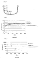
- the outline of the obtained hollow cathode sputtering target is shown in FIG. 1.
- the measurement of the surface roughness of the target was conducted at the respective measurement points (1 to 6) shown in FIG. 1.
- Table 1 shows the surface roughness Ra( ⁇ m) of the inside of the target. As shown in Table 1, the surface roughness Ra of the bottom face corresponding to the measurement points 1 to 6 is 0.5 ⁇ m or less, and the surface roughness Ra of the cylindrical inner peripheral face was also 0.5 ⁇ m or less.
- the inside face of a Ti hollow cathode target was finished by being subject to lathe processing, polishing (sandpapering) and etching so as to be Ra ( ⁇ m) ⁇ 1.0.
- Example 2 the measurement of the surface roughness of the target was conducted at the respective measurement points (1 to 6) shown in FIG. 1. The results are similarly shown in Table 1.
- the surface roughness Ra of the bottom face corresponding to the measurement points 1 to 6 is 1.0 ⁇ m or less, and the surface roughness Ra of the cylindrical inner peripheral face was also 1.0 ⁇ m or less.
- FIG. 2 and FIG. 3 The results upon performing a sputtering test with this hollow cathode target are shown in FIG. 2 and FIG. 3. As shown in FIG. 2, the uniformity showed favorable values from the initial stage. Also, as shown in FIG. 3, there were roughly 2,500 particles on a single wafer. Further, peeling of the redeposited film at the bottom of the inside face could not be observed up to the expected useful life.
- the inside face of a Ti hollow cathode target was finished with only lathe processing.
- the measurement of the surface roughness of the target was conducted at the respective measurement points (1 to 6) shown in FIG. 1.
- the surface roughness Ra ( ⁇ m) of the inside face of the target is shown in Table 1.
- Results of the sputtering test are related to Examples 1 and 2, and the measurement results of uniformity and the number of particles are shown in FIG. 2 and FIG. 3.
- the uniformity is inferior from the initial stage, and the number of particles on a single wafer was larger in comparison to Examples 1 and 2 at 25,000 particles. Further, after the use of roughly 8000kWhr, peeling of the redeposited layer on the bottom of the inside face was confirmed.
- the inside face of a Ta hollow cathode target was finished by being subject to lathe processing, polishing (sandpapering) and etching.
- the measurement of the surface roughness of the target was conducted at the respective measurement points (1 to 6) shown in FIG. 1.
- the surface roughness Ra ( ⁇ m) of the inside face of the target is shown in Table 1. As shown in Table 1, the surface roughness Ra at the measurement points 1 to 6 was 0.4 to 0.5 ⁇ m.
- the inside face of a Ta hollow cathode target was finished by being subject to lathe processing, polishing and etching.
- the measurement of the surface roughness of the target was conducted at the respective measurement points (1 to 6) shown in FIG. 1.
- the surface roughness Ra ( ⁇ m) of the inside face of the target is shown in Table 1. As shown in Table 1, the surface roughness Ra at the measurement points 1 to 6 was 0.7 to 1.0 ⁇ m.
- the inside face of a Ta hollow cathode target was finished with only lathe processing.
- the measurement of the surface roughness of the target was conducted at the respective measurement points (1 to 6) shown in FIG. 1.
- the surface roughness Ra ( ⁇ m) of the inside face of the target is shown in Table 1.
- Results of the sputtering test are related to Examples 3 and 4, and the measurement results of uniformity and the number of particles are shown in FIG. 4 and FIG. 5.
- the uniformity is inferior from the initial stage, and the number of particles on a single wafer was larger in comparison to Examples 3 and 4 at 6,000 particles. Further, peeling of the redeposited layer on the bottom of the inside face was confirmed after the expected useful life.
- the present invention is advantageous in that the function of a hollow cathode sputtering target can be further improved since a target which has superior sputter film evenness (uniformity), generates few arcing and particles, is capable of suppressing the peeling of the redeposited film on the bottom face, and has superior deposition characteristics can be manufactured.
Landscapes
- Chemical & Material Sciences (AREA)
- Chemical Kinetics & Catalysis (AREA)
- Engineering & Computer Science (AREA)
- Materials Engineering (AREA)
- Mechanical Engineering (AREA)
- Metallurgy (AREA)
- Organic Chemistry (AREA)
- Physical Vapour Deposition (AREA)
Abstract
Description
- The present invention relates to a hollow cathode sputtering target which generates few particles and which has superior surface cleansability, and to a surface finishing method of this target.
- In recent years, the sputtering method for forming a film from materials such as metal or ceramics has been used in numerous fields such as electronics, corrosion resistant materials and ornaments, catalysts, as well as in the manufacture of cutting/grinding materials and abrasion resistant materials.
- Although the sputtering method itself is a well-known method in the foregoing fields, recently, particularly in the electronics field, a sputtering target suitable for forming films of complex shapes and forming circuits is in demand.
- Under these circumstances, a hollow cathode sputtering target has been proposed recently. This target is formed in the shape of a cup, and is referred to as a hollow cathode sputtering target based on such shape (e.g., refer to
Patent Documents - With this hollow cathode sputtering target, high density plasma can be generated within the target, and, by further providing directivity in the sputtering direction, a via hole can be filled at a high aspect ratio without having to use a conventional collimator.
- As described above, a hollow cathode sputtering target has a function of a deposition method that is effective and easier to control in comparison to a conventional planar target.
- Generally speaking, on the inside of a hollow cathode sputtering target, there are an erosion area to where a target is sputtered and a deposition area to where the sputtered atoms are deposited.
- Ordinarily, a deposition area is formed at the bottom face, and there is a significant problem in that the redeposited film will easily peel in the vicinity of the deposition area, and contaminate the substrate by flying to or dropping on the substrate.
- Generally, when using a planar target, the erosion face of the target is cleansed, the work-affected layer is removed and the surface roughness is reduced so as to suppress the generation of particles.
- Meanwhile, when there is a target face or peripheral equipment that is not eroded, contrarily, a measure is adopted such as roughening the surface so as to capture the physical matter that comes flying from the target during sputtering (e.g., refer to
Patent Document - Patent Document 1: Japanese Patent Laid-Open Publication No. 2000-256843
- Patent Document 2: Japanese Patent Laid-Open Publication No. 2001-98367
- Patent Document 3: Publication No. 2002-531690 of Translation of International Application
- Patent Document 4: Japanese Patent Laid-Open Publication No. H4-304367
- Patent Document 5: Japanese Patent Laid-Open Publication No. H11-1766
- Patent Document 6: Japanese Patent Laid-Open Publication No. H173965
- Nevertheless, this kind of technology was applied in a hollow cathode sputtering target to roughen the bottom face of the target so as to prevent the peeling of the deposited material (redeposited film), but was unsuccessful. Contrarily, at the stage of commencing the sputtering process, the result was such that the uniformity of deposition was unstable, and numerous particles were generated.
- Therefore, there was no choice but to use a conventional hollow cathode sputtering target, and there are problems in that the evenness (uniformity) of the film is inferior, arcing and particles are generated, and the quality of the sputtered deposition will deteriorate.
- Thus, an object of the present invention is to provide a hollow cathode sputtering target which has superior sputter film evenness (uniformity), generates few arcing and particles, is capable of suppressing the peeling of the redeposited film on the bottom face, and has superior deposition characteristics, as well as a method for stably manufacturing this target.
- In order to achieve the foregoing object, the present inventors discovered that by improving/devising the inner bottom face of the hollow cathode sputtering target, a hollow cathode sputtering target which has superior sputter film evenness (uniformity), generates few arcing and particles, is capable of suppressing the peeling of the redeposited film on the bottom face, and has superior deposition characteristics, as well as a method for stably manufacturing this target, could be obtained.
- Based on the foregoing discovery, the present invention provides:
- 1. A hollow cathode sputtering target comprising an inner bottom face having a surface roughness of Ra≦1.0µm, preferably Ra≦0.5µm.
- 2. The hollow cathode sputtering target according to
paragraph 1, comprising a bottom face having a surface roughness Ra equal to or less than a cylindrical inner peripheral face; - 3. The hollow cathode sputtering target according to any one of
paragraph 1 orparagraph 2 above, comprising a rough face at the outer peripheral edge; - 4. The hollow cathode sputtering target according to
paragraph 3 above, comprising a rough face formed by performing abrasive blasting to the outer peripheral edge; - 5. The [hollow cathode] sputtering target according to any one of
paragraphs 1 to 4 above, wherein the target is formed from a cladding material; - 6. A surface finishing method of a hollow cathode sputtering target characterizing in polishing and etching the bottom face of the target so as to make the surface roughness of the inner bottom face Ra≦1.0µm, preferably Ra≦0.5µm
- The present invention yields a superior effect in that it is able to stably obtain a hollow cathode sputtering target which has superior film evenness (uniformity) from the initial stages of sputtering, generates few arcing and particles, is superior deposition characteristics, and favorable target usability.
- Further, there is another significant effect of being able to considerably reduce the peeling of the redeposited from the inner bottom face of a hollow cathode target which was in particular a problem heretofore.
-
- FIG. 1 is a schematic diagram of the cross section and planar surface of the hollow cathode sputtering target showing the respective measurement points of the surface roughness;
- FIG. 2 is a diagram showing the uniformity upon sputtering a hollow cathode Ti target;
- FIG. 3 is a diagram showing the generation of particles upon sputtering a hollow cathode Ti target;
- FIG. 4 is a diagram showing the uniformity upon sputtering a hollow cathode Ta target; and
- FIG. 5 is a diagram showing the generation of particles upon sputtering a hollow cathode Ta target;
- The hollow cathode sputtering target of the present invention can be applied to ceramics of various metals, alloys, silicides and oxides, but there is no particular limitation to the material. In order to manufacture a hollow body (cup shape), processing methods such as forging, flattening, rolling, deep drawing or the like are employed. There is also no particular limitation to this manufacturing method.
- Upon manufacture, what is particularly important is the surface finishing of the inside of the target. In other words, after forming the hollow cathode sputtering target, it is important to subject the bottom face of the target to lathe processing, polishing and etching so as to make the surface roughness of the bottom face Ra≦ 1.0µm, preferably Ra≦0.5µm.
- With a sputtering target comprising an inner bottom face having a surface roughness of Ra≦1.0µm, preferably Ra≦0.5µm, in particular, it is desirable to comprise a bottom face having a surface roughness Ra equal to or less than the cylindrical inner peripheral face.
- Meanwhile, it is also desirable that the erosion face also has a surface roughness of at least Ra≦1.0µm, preferably Ra≦0.5µm.
- Further, the outer peripheral edge or outer peripheral face of the hollow cathode sputtering target is a non-erosion face, and it is desirable that such edge or face has a rough face. This will usually become a getter for capturing particles.
- The hollow cathode sputtering target may be a single body, or the target may be formed from a cladding material. The inner bottom face of the hollow cathode sputtering target is required to have the same surface roughness as above; namely, Ra≦1.0µm, preferably Ra≦0.5µm.
- Although a curved face exists at the boundary of the bottom face and cylindrical inner face of the hollow cathode target, in the present invention, it is desirable that such curved portion is also polished such that the surface roughness of the surface thereof become Ra≦1.0µm, preferably Ra≦0.5µm.
- The present invention is now explained in detail with reference to the Examples. Incidentally, these Examples are merely illustrative, and the present invention shall in no way be limited thereby. In other words, the present invention shall include the various modes and modifications contained in the technical spirit of this invention.
- The inside face of a Ti hollow cathode target was finished by being subject to lathe processing, polishing (sandpapering) and etching. The outline of the obtained hollow cathode sputtering target is shown in FIG. 1. The measurement of the surface roughness of the target was conducted at the respective measurement points (1 to 6) shown in FIG. 1.
- Table 1 shows the surface roughness Ra(µm) of the inside of the target. As shown in Table 1, the surface roughness Ra of the bottom face corresponding to the measurement points 1 to 6 is 0.5µm or less, and the surface roughness Ra of the cylindrical inner peripheral face was also 0.5µm or less.
- The results upon performing a sputtering test with this hollow cathode target are shown in FIG. 2 and FIG. 3. The uniformity showed favorable values from the initial stage, and there were roughly 900 particles on a single wafer. Further, peeling of the redeposited film of the inner bottom could not be observed up to the expected useful life.
Table 1 Example 1 Example 2. Comparative Example 1 Example 3 Example 4 Comparative Example 2 (1) 0.4 0.7 1.7 0.5 0.8 3.5 (2) 0.4 0.8 1.7 0.5 0.9 2.3 (3) 0.4 0.8 1.0 0.4 0.8 2.0 (4) 0.4 0.7 2.1 0.5 0.7 2.6 (5) 0.3 0.7 2.5 0.4 0.8 2.4 (6) 0.4 0.8 1.3 0.5 1.0 3.5 Ra(µm) - The inside face of a Ti hollow cathode target was finished by being subject to lathe processing, polishing (sandpapering) and etching so as to be Ra (µ m)< 1.0.
- As with Example 1, the measurement of the surface roughness of the target was conducted at the respective measurement points (1 to 6) shown in FIG. 1. The results are similarly shown in Table 1.
- As shown in Table 1, the surface roughness Ra of the bottom face corresponding to the measurement points 1 to 6 is 1.0 µ m or less, and the surface roughness Ra of the cylindrical inner peripheral face was also 1.0 µ m or less.
- The results upon performing a sputtering test with this hollow cathode target are shown in FIG. 2 and FIG. 3. As shown in FIG. 2, the uniformity showed favorable values from the initial stage. Also, as shown in FIG. 3, there were roughly 2,500 particles on a single wafer. Further, peeling of the redeposited film at the bottom of the inside face could not be observed up to the expected useful life.
- The inside face of a Ti hollow cathode target was finished with only lathe processing. As with Example 1, the measurement of the surface roughness of the target was conducted at the respective measurement points (1 to 6) shown in FIG. 1.
- Similarly, the surface roughness Ra (µm) of the inside face of the target is shown in Table 1. As shown in Table 1, the surface roughness corresponding to the measurement points 1 to 6 was bottom face Ra = 1.3 to 2.5 µm, and side face Ra = 1.0 to 1.7 µm.
- Results of the sputtering test are related to Examples 1 and 2, and the measurement results of uniformity and the number of particles are shown in FIG. 2 and FIG. 3.
- As shown in FIG. 2 and FIG. 3, the uniformity is inferior from the initial stage, and the number of particles on a single wafer was larger in comparison to Examples 1 and 2 at 25,000 particles. Further, after the use of roughly 8000kWhr, peeling of the redeposited layer on the bottom of the inside face was confirmed.
- The inside face of a Ta hollow cathode target was finished by being subject to lathe processing, polishing (sandpapering) and etching. As with Example 1, the measurement of the surface roughness of the target was conducted at the respective measurement points (1 to 6) shown in FIG. 1.
- The surface roughness Ra (µm) of the inside face of the target is shown in Table 1. As shown in Table 1, the surface roughness Ra at the measurement points 1 to 6 was 0.4 to 0.5µm.
- As a result of performing a sputtering test with this hollow cathode target, as shown in FIG. 4, the uniformity showed favorable values from the initial stage. Also, as shown in FIG. 5, there were roughly 500 particles on a single wafer. Further, peeling of the redeposited film at the bottom of the inside face could not be observed up to the expected useful life.
- The inside face of a Ta hollow cathode target was finished by being subject to lathe processing, polishing and etching. As with Example 1, the measurement of the surface roughness of the target was conducted at the respective measurement points (1 to 6) shown in FIG. 1.
- The surface roughness Ra (µ m) of the inside face of the target is shown in Table 1. As shown in Table 1, the surface roughness Ra at the measurement points 1 to 6 was 0.7 to 1.0µm.
- As a result of performing a sputtering test with this hollow cathode target, as shown in FIG. 4, the uniformity showed favorable values from the initial stage. Also, as shown in FIG. 5, there were roughly 1,800 particles on a single wafer. Further, peeling of the redeposited film at the bottom of the inside face could not be observed up to the expected useful life.
- The inside face of a Ta hollow cathode target was finished with only lathe processing. As with Example 1, the measurement of the surface roughness of the target was conducted at the respective measurement points (1 to 6) shown in FIG. 1.
- Similarly, the surface roughness Ra (µ m) of the inside face of the target is shown in Table 1. As shown in Table 1, the surface roughness corresponding to the measurement points 1 to 6 was bottom face Ra = 2.4 to 3.5 µ m, and side face Ra = 2 .0 to 3.5 µ m .
- Results of the sputtering test are related to Examples 3 and 4, and the measurement results of uniformity and the number of particles are shown in FIG. 4 and FIG. 5.
- As shown in FIG. 4 and FIG. 5, the uniformity is inferior from the initial stage, and the number of particles on a single wafer was larger in comparison to Examples 3 and 4 at 6,000 particles. Further, peeling of the redeposited layer on the bottom of the inside face was confirmed after the expected useful life.
- The present invention is advantageous in that the function of a hollow cathode sputtering target can be further improved since a target which has superior sputter film evenness (uniformity), generates few arcing and particles, is capable of suppressing the peeling of the redeposited film on the bottom face, and has superior deposition characteristics can be manufactured.
Claims (8)
- A hollow cathode sputtering target comprising an inner bottom face having a surface roughness of Ra≦1.0µm.
- A hollow cathode sputtering target comprising an inner bottom face having a surface roughness of Ra≦0.5µm.
- The hollow cathode sputtering target according to claim 1 or claim 2, comprising a bottom face having a surface roughness Ra equal to or less than a cylindrical inner peripheral face.
- The hollow cathode sputtering target according to any one of claims 1 to 3, comprising a rough face at the outer peripheral edge.
- The hollow cathode puttering target according to claim 4, comprising a rough face formed by performing abrasive blasting to the outer peripheral edge.
- The hollow cathode sputtering target according to any one of claims 1 to 5, wherein the target is formed from a cladding material.
- A surface finishing method of a hollow cathode sputtering target characterized in polishing and etching the bottom face of the target so as to make the surface roughness of the inner bottom face Ra≦1.0µm.
- A surface finishing method of a hollow cathode sputtering target characterized in polishing and etching the bottom face of the target so as to make the surface roughness of the inner bottom face Ra≦0.5µm.
Applications Claiming Priority (2)
| Application Number | Priority Date | Filing Date | Title |
|---|---|---|---|
| JP2003321050 | 2003-09-12 | ||
| PCT/JP2004/012083 WO2005026407A1 (en) | 2003-09-12 | 2004-08-24 | Sputtering target and method for finishing surface of such target |
Publications (2)
| Publication Number | Publication Date |
|---|---|
| EP1666630A1 true EP1666630A1 (en) | 2006-06-07 |
| EP1666630A4 EP1666630A4 (en) | 2012-06-27 |
Family
ID=34308622
Family Applications (1)
| Application Number | Title | Priority Date | Filing Date |
|---|---|---|---|
| EP04772044A Ceased EP1666630A4 (en) | 2003-09-12 | 2004-08-24 | SPRAY TARGET AND SURFACE FINISHING METHOD OF SUCH A TARGET |
Country Status (7)
| Country | Link |
|---|---|
| US (1) | US7951275B2 (en) |
| EP (1) | EP1666630A4 (en) |
| JP (1) | JP4468302B2 (en) |
| KR (1) | KR100727243B1 (en) |
| CN (1) | CN1823178B (en) |
| TW (1) | TWI288181B (en) |
| WO (1) | WO2005026407A1 (en) |
Families Citing this family (15)
| Publication number | Priority date | Publication date | Assignee | Title |
|---|---|---|---|---|
| US20030002043A1 (en) * | 2001-04-10 | 2003-01-02 | Kla-Tencor Corporation | Periodic patterns and technique to control misalignment |
| CN1329552C (en) * | 2001-11-26 | 2007-08-01 | 日矿金属株式会社 | Sputtering target and manufacturing method thereof |
| US8296562B2 (en) * | 2004-07-15 | 2012-10-23 | Anakam, Inc. | Out of band system and method for authentication |
| EP1865090B1 (en) * | 2005-03-28 | 2010-04-07 | Nippon Mining & Metals Co., Ltd. | Deep-pot-shaped copper sputtering target |
| US20080078268A1 (en) | 2006-10-03 | 2008-04-03 | H.C. Starck Inc. | Process for preparing metal powders having low oxygen content, powders so-produced and uses thereof |
| US20080145688A1 (en) | 2006-12-13 | 2008-06-19 | H.C. Starck Inc. | Method of joining tantalum clade steel structures |
| TWI432592B (en) * | 2007-04-27 | 2014-04-01 | Honeywell Int Inc | Sputtering targets having reduced burn-in time, their methods of production and uses thereof |
| US8197894B2 (en) | 2007-05-04 | 2012-06-12 | H.C. Starck Gmbh | Methods of forming sputtering targets |
| WO2009099121A1 (en) * | 2008-02-08 | 2009-08-13 | Nippon Mining & Metals Co., Ltd. | Ytterbium sputtering target and method for manufacturing the target |
| DE102008019202A1 (en) | 2008-04-17 | 2009-10-22 | Kennametal Inc. | Coating method, workpiece or tool and its use |
| US8246903B2 (en) | 2008-09-09 | 2012-08-21 | H.C. Starck Inc. | Dynamic dehydriding of refractory metal powders |
| WO2013049274A2 (en) | 2011-09-29 | 2013-04-04 | H.C. Starck, Inc. | Large-area sputtering targets and methods of manufacturing large-area sputtering targets |
| WO2013070679A1 (en) | 2011-11-08 | 2013-05-16 | Tosoh Smd, Inc. | Silicon sputtering target with special surface treatment and good particle performance and methods of making the same |
| WO2016027599A1 (en) * | 2014-08-22 | 2016-02-25 | 三井金属鉱業株式会社 | Method for manufacturing target material for cylindrical sputtering target and cylindrical sputtering target |
| CN111421063B (en) * | 2020-04-10 | 2022-02-18 | 宁波江丰电子材料股份有限公司 | Pot-shaped target material processing and forming method |
Family Cites Families (17)
| Publication number | Priority date | Publication date | Assignee | Title |
|---|---|---|---|---|
| WO1992004482A1 (en) * | 1990-08-30 | 1992-03-19 | Materials Research Corporation | Pretextured cathode sputtering target and method of preparation thereof and sputtering therewith |
| US5482611A (en) * | 1991-09-30 | 1996-01-09 | Helmer; John C. | Physical vapor deposition employing ion extraction from a plasma |
| US5687600A (en) * | 1994-10-26 | 1997-11-18 | Johnson Matthey Electronics, Inc. | Metal sputtering target assembly |
| JPH09209135A (en) * | 1996-02-01 | 1997-08-12 | Mitsubishi Materials Corp | Target for magnetron sputtering |
| DE19634312A1 (en) * | 1996-08-24 | 1998-02-26 | Behringwerke Ag | Process for producing factor V deficient plasma and a deficient plasma obtained in this way |
| JP3755559B2 (en) * | 1997-04-15 | 2006-03-15 | 株式会社日鉱マテリアルズ | Sputtering target |
| US6139701A (en) * | 1997-11-26 | 2000-10-31 | Applied Materials, Inc. | Copper target for sputter deposition |
| EP1135233A4 (en) | 1998-12-03 | 2004-11-03 | Tosoh Smd Inc | Insert target assembly and method of making same |
| JP2000233865A (en) * | 1999-02-16 | 2000-08-29 | Chuo Densetsu Kk | Dispenser for adhesive tape |
| US6283357B1 (en) * | 1999-08-03 | 2001-09-04 | Praxair S.T. Technology, Inc. | Fabrication of clad hollow cathode magnetron sputter targets |
| US6342133B2 (en) * | 2000-03-14 | 2002-01-29 | Novellus Systems, Inc. | PVD deposition of titanium and titanium nitride layers in the same chamber without use of a collimator or a shutter |
| JP4761605B2 (en) * | 2000-05-09 | 2011-08-31 | 株式会社東芝 | Sputtering target |
| US6503380B1 (en) * | 2000-10-13 | 2003-01-07 | Honeywell International Inc. | Physical vapor target constructions |
| US6887356B2 (en) * | 2000-11-27 | 2005-05-03 | Cabot Corporation | Hollow cathode target and methods of making same |
| JP2002302762A (en) * | 2001-04-04 | 2002-10-18 | Tosoh Corp | ITO sputtering target |
| CN1329552C (en) * | 2001-11-26 | 2007-08-01 | 日矿金属株式会社 | Sputtering target and manufacturing method thereof |
| US7297247B2 (en) * | 2003-05-06 | 2007-11-20 | Applied Materials, Inc. | Electroformed sputtering target |
-
2004
- 2004-08-24 US US10/566,301 patent/US7951275B2/en active Active
- 2004-08-24 KR KR1020067004596A patent/KR100727243B1/en not_active Expired - Lifetime
- 2004-08-24 JP JP2005513825A patent/JP4468302B2/en not_active Expired - Lifetime
- 2004-08-24 EP EP04772044A patent/EP1666630A4/en not_active Ceased
- 2004-08-24 CN CN2004800201804A patent/CN1823178B/en not_active Expired - Lifetime
- 2004-08-24 WO PCT/JP2004/012083 patent/WO2005026407A1/en not_active Ceased
- 2004-08-30 TW TW093126010A patent/TWI288181B/en not_active IP Right Cessation
Also Published As
| Publication number | Publication date |
|---|---|
| TWI288181B (en) | 2007-10-11 |
| US20070108046A1 (en) | 2007-05-17 |
| KR100727243B1 (en) | 2007-06-11 |
| WO2005026407A1 (en) | 2005-03-24 |
| TW200510558A (en) | 2005-03-16 |
| CN1823178B (en) | 2011-06-22 |
| EP1666630A4 (en) | 2012-06-27 |
| US7951275B2 (en) | 2011-05-31 |
| KR20060061369A (en) | 2006-06-07 |
| CN1823178A (en) | 2006-08-23 |
| JP4468302B2 (en) | 2010-05-26 |
| JPWO2005026407A1 (en) | 2007-11-08 |
Similar Documents
| Publication | Publication Date | Title |
|---|---|---|
| US9034154B2 (en) | Sputtering target and process for producing same | |
| US7951275B2 (en) | Sputtering target and method for finishing surface of such target | |
| US7909949B2 (en) | Sputtering target with few surface defects, and surface processing method thereof | |
| US8936706B2 (en) | Sputtering target with low generation of particles | |
| US7732056B2 (en) | Corrosion-resistant aluminum component having multi-layer coating | |
| US6193821B1 (en) | Fine grain tantalum sputtering target and fabrication process | |
| JP5744958B2 (en) | Ytterbium sputtering target | |
| EP1591556A1 (en) | Ta SPUTTERING TARGET AND METHOD FOR PREPARATION THEREOF | |
| US20120273347A1 (en) | Sputtering target with reduced particle generation and method of producing said target | |
| EP1018566B1 (en) | Sputtering target and method for the manufacture thereof | |
| EP2123791A1 (en) | Deep-pot-shaped copper sputtering target and process for producing the same | |
| WO2008060917A9 (en) | Methods for making sputtering targets | |
| US20070056688A1 (en) | Methods of treating deposition process components to form particle traps, and deposition process components having particle traps thereon | |
| WO2006059429A1 (en) | Sb-Te BASE ALLOY SINTERED SPATTERING TARGET | |
| CN112828541A (en) | Tantalum target material and processing method of sputtering surface thereof | |
| EP1087033A1 (en) | Extended life sputter targets | |
| JP7784393B2 (en) | Wafer Support | |
| JP2003166053A (en) | Sputtering target | |
| WO2005026408A2 (en) | Methods of treating components of a deposition apparatus to form particle traps, and such components having particle traps thereon | |
| WO2005077677A1 (en) | Physical vapor deposition components, and methods of treating components |
Legal Events
| Date | Code | Title | Description |
|---|---|---|---|
| PUAI | Public reference made under article 153(3) epc to a published international application that has entered the european phase |
Free format text: ORIGINAL CODE: 0009012 |
|
| 17P | Request for examination filed |
Effective date: 20060111 |
|
| AK | Designated contracting states |
Kind code of ref document: A1 Designated state(s): DE |
|
| RAP1 | Party data changed (applicant data changed or rights of an application transferred) |
Owner name: NIPPON MINING & METALS CO., LTD. |
|
| DAX | Request for extension of the european patent (deleted) | ||
| RBV | Designated contracting states (corrected) |
Designated state(s): DE |
|
| RAP1 | Party data changed (applicant data changed or rights of an application transferred) |
Owner name: JX NIPPON MINING & METALS CORPORATION |
|
| A4 | Supplementary search report drawn up and despatched |
Effective date: 20120530 |
|
| RIC1 | Information provided on ipc code assigned before grant |
Ipc: C23C 14/34 20060101AFI20120523BHEP |
|
| 17Q | First examination report despatched |
Effective date: 20120919 |
|
| REG | Reference to a national code |
Ref country code: DE Ref legal event code: R003 |
|
| STAA | Information on the status of an ep patent application or granted ep patent |
Free format text: STATUS: THE APPLICATION HAS BEEN REFUSED |
|
| 18R | Application refused |
Effective date: 20200113 |