EP1662559A2 - Chucking method and processing method using the same - Google Patents
Chucking method and processing method using the same Download PDFInfo
- Publication number
- EP1662559A2 EP1662559A2 EP05026071A EP05026071A EP1662559A2 EP 1662559 A2 EP1662559 A2 EP 1662559A2 EP 05026071 A EP05026071 A EP 05026071A EP 05026071 A EP05026071 A EP 05026071A EP 1662559 A2 EP1662559 A2 EP 1662559A2
- Authority
- EP
- European Patent Office
- Prior art keywords
- layer
- stage
- chucking
- insulator
- conductive
- Prior art date
- Legal status (The legal status is an assumption and is not a legal conclusion. Google has not performed a legal analysis and makes no representation as to the accuracy of the status listed.)
- Granted
Links
Images



Classifications
-
- H—ELECTRICITY
- H10—SEMICONDUCTOR DEVICES; ELECTRIC SOLID-STATE DEVICES NOT OTHERWISE PROVIDED FOR
- H10P—GENERIC PROCESSES OR APPARATUS FOR THE MANUFACTURE OR TREATMENT OF DEVICES COVERED BY CLASS H10
- H10P95/00—Generic processes or apparatus for manufacture or treatments not covered by the other groups of this subclass
-
- H—ELECTRICITY
- H10—SEMICONDUCTOR DEVICES; ELECTRIC SOLID-STATE DEVICES NOT OTHERWISE PROVIDED FOR
- H10P—GENERIC PROCESSES OR APPARATUS FOR THE MANUFACTURE OR TREATMENT OF DEVICES COVERED BY CLASS H10
- H10P72/00—Handling or holding of wafers, substrates or devices during manufacture or treatment thereof
- H10P72/70—Handling or holding of wafers, substrates or devices during manufacture or treatment thereof for supporting or gripping
- H10P72/72—Handling or holding of wafers, substrates or devices during manufacture or treatment thereof for supporting or gripping using electrostatic chucks
- H10P72/722—Details of electrostatic chucks
-
- H—ELECTRICITY
- H02—GENERATION; CONVERSION OR DISTRIBUTION OF ELECTRIC POWER
- H02N—ELECTRIC MACHINES NOT OTHERWISE PROVIDED FOR
- H02N13/00—Clutches or holding devices using electrostatic attraction, e.g. using Johnson-Rahbek effect
-
- H—ELECTRICITY
- H10—SEMICONDUCTOR DEVICES; ELECTRIC SOLID-STATE DEVICES NOT OTHERWISE PROVIDED FOR
- H10P—GENERIC PROCESSES OR APPARATUS FOR THE MANUFACTURE OR TREATMENT OF DEVICES COVERED BY CLASS H10
- H10P72/00—Handling or holding of wafers, substrates or devices during manufacture or treatment thereof
- H10P72/50—Handling or holding of wafers, substrates or devices during manufacture or treatment thereof for positioning, orientation or alignment
-
- H—ELECTRICITY
- H10—SEMICONDUCTOR DEVICES; ELECTRIC SOLID-STATE DEVICES NOT OTHERWISE PROVIDED FOR
- H10P—GENERIC PROCESSES OR APPARATUS FOR THE MANUFACTURE OR TREATMENT OF DEVICES COVERED BY CLASS H10
- H10P72/00—Handling or holding of wafers, substrates or devices during manufacture or treatment thereof
- H10P72/70—Handling or holding of wafers, substrates or devices during manufacture or treatment thereof for supporting or gripping
- H10P72/72—Handling or holding of wafers, substrates or devices during manufacture or treatment thereof for supporting or gripping using electrostatic chucks
Definitions
- the invention relates to an electrostatic chucking technology used in a semiconductor device manufacturing process or a liquid crystal panel manufacturing process.
- an electrostatic chucking method is used as a method of chucking a semiconductor wafer on a stage of an etching apparatus and so on in each of processes such as etching, CVD (chemical vapor deposition), PVD (physical vapor deposition), and so on.
- This electrostatic chucking method is to apply a voltage between a stage and a semiconductor wafer set on this stage with a dielectric layer therebetween to chuck the semiconductor wafer on the stage with static electricity generated therebetween.
- an electrostatic chucking type apparatus a workpiece formed of an insulator can not be chucked on a stage. Therefore, it is necessary to chuck such a workpiece by a mechanical clamp mechanism in an apparatus that performs processes in a vacuum state, such as a etching apparatus, a CVD apparatus, or a PVD apparatus.
- a clamp mechanism causes instability of the temperature distribution in the workpiece and reduction of processing accuracy by the workpiece warping, thereby reducing the yield.
- an electrostatic chucking technology capable of chucking a workpiece formed of an insulator or a workpiece attached with an object to be processed such as a semiconductor wafer on the stage has been required. It is thus an object of the invention to provide an improved method of chucking.
- the invention provides a method of chucking.
- the method includes providing an object having a surface portion that is made of an insulator, attaching a member with a conductive layer to the surface portion, placing the object to which the member is attached in a vacuum chamber, and chucking the object to a stage provided in the vacuum chamber by generating electrostatic charges between the member and the stage.
- the invention provides another method of chucking.
- the method includes providing an object for chucking, attaching a substrate made of an insulator to the object, attaching a member with a conductive layer to the substrate, placing the object to which the member and the substrate are attached in a vacuum chamber, and chucking the object to a stage provided in the vacuum chamber by generating electrostatic charges between the member and the stage.
- the invention also provides a method of processing objects.
- the method includes providing an object having a surface portion that is made of an insulator, attaching a member with a conductive layer to the surface portion, placing the object to which the member is attached in a vacuum chamber, chucking the object to a stage provided in the vacuum chamber by generating electrostatic charges between the member and the stage, and processing the object chucked to the stage in the vacuum chamber.
- the invention provides another method of processing an object.
- the method includes attaching a substrate made of an insulator to the object, attaching a member with a conductive layer to the substrate, placing the object to which the member and the substrate are attached in a vacuum chamber, chucking the object to a stage provided in the vacuum chamber by generating electrostatic charges between the member and the stage, and processing the object chucked to the stage in the vacuum chamber.
- a conductive film used in an embodiment of the invention will be described as an example of a conductive member with reference to figures.
- Figs. 1A, 1B, and 1C are cross-sectional views showing a structure of the conductive film.
- a conductive film 9 shown in Fig. 1A is formed of a protection layer 1, a conductive layer 2, an attachment layer 3, and a separation layer 4 laminated in this order.
- the conductive film 9 is formed of the protection layer 1, the conductive layer 2, a polyimide layer 5, the attachment layer 3, and the separation layer 4 laminated in this order.
- the protection layer 1 is a plastic film formed of a plastic material such as polyethylene, polypropylene, polyvinyl chloride, polystyrene, polyethylene terephthalate, polyacrylonitrile, or the like.
- the conductive layer 2 is formed of a conductive polymer containing conjugated double bonds in its molecular structure, such as polypyrrole or the like.
- the attachment layer 3 is formed of an adhesive such as an acrylic type adhesive, a urethane type adhesive, a synthetic rubber type adhesive, or the like.
- the separation layer 4 is a release paper or the like, and separated when the conductive film 9 is used.
- the conductive film 9A shown in Fig. 1B is formed of the protection layer 1, the polyimide layer 5, the conductive layer 2, the attachment layer 3, and the separation layer 4 laminated in this order. Since polyimide has high thermal resistance, using the conductive film having such high thermal resistance can provide stable chucking characteristics even at high temperature.
- the conductive film 9B shown in Fig. 1C is formed of the protection layer 1, a polymer layer 6 formed by polymerizing a conductive material and polyimide, the attachment layer 3, and the separation layer 4 laminated in this order.
- the attachment layer 3 in Figs. 1B and 1C is preferably formed of a material having thermal resistance.
- a layered body 15 includes a semiconductor substrate 7 and a glass substrate 8 for supporting the semiconductor substrate 7.
- the layered body 15 is the object to be chucked. It is noted that electronic devices are formed on the surface of the semiconductor substrate 7.
- the separation layer 4 of the conductive film 9 is separated and removed to expose the attachment layer 3, so that the conductive film 9 is attached to the glass substrate 8 with this attachment layer 3 therebetween.
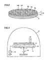
- the layered body 15 forms a shape of a disk-like semiconductor wafer.
- the semiconductor substrate 7 has a large number of semiconductor integrated circuits 100 sectioned in a matrix by a dicing line DL.
- the glass substrate 8 is used as a supporting body of the semiconductor substrate 7, the other insulator of a ceramic, quartz, a plastic, or a resin, e.g., a resist or an epoxy resin, can be used as the supporting body.
- the layered body 15 attached with the conductive film 9 is set on a stage 10 set in a vacuum chamber 12 of a dry-etching apparatus or the like. At this time, the surface of the stage 10 is covered with a dielectric layer (not shown).
- a power supply 13 is to supply a DC voltage or an AC voltage to an internal electrode, and an AC power supply 14 is to supply an AC voltage to the stage 10.
- the layered body 15 is set on the stage 10, a voltage is applied to an internal electrode 11 provided in the stage 10 to generate positive and negative electric charges on the surfaces of the conductive film 9 and the stage 10, and the layered body 15 is chucked on the stage 10 with static electricity generated therebetween. Then, the semiconductor substrate 7 of the chucked layered body 15 is processed by dry-etching, CVD (chemical vapor deposition), or PVD (physical vapor deposition), in a vacuum state.
- CVD chemical vapor deposition
- PVD physical vapor deposition
- Figs. 4A to 6 are partial cross-sectional views of the layered body 15 in process order.
- a pad electrode 20 as well as electronic devices (not shown) (e.g. a CCD (Charge Coupled Device), a light receiving element such as an infrared ray sensor, or a light emissive element) is formed on a front surface of the semiconductor substrate 7, the pad electrode 20 being connected with these electronic devices.
- the pad electrode 20 is formed on the front surface of the semiconductor substrate 7 with an interlayer insulation film 21 therebetween.
- the semiconductor substrate 7 is formed of, for example, silicon (Si), and preferably has a thickness of about 20 to 200 ⁇ m.
- the pad electrode 20 is formed of, for example, aluminum (Al), and preferably has a thickness of about 1 ⁇ m. It is noted that a passivation film (not shown) is formed on the semiconductor substrate 7, covering at least a part of the pad electrode 20.
- the interlayer insulation film 21 is formed of, for example, an oxide film, and preferably has a thickness of about 0.8 ⁇ m. Then, the glass substrate 8 having a thickness of about 80 to 100 ⁇ m is attached on the front surface of the semiconductor substrate 7 with a resin layer 22 therebetween. The conductive film 9 is then attached to the front surface of the glass substrate 8.
- a resist layer 23 is selectively formed on a back surface of the semiconductor substrate 7.
- the layered body 15 formed with the resist layer 23 and attached with the conductive film 9 is set on the stage 10 in the vacuum chamber 12 of the dry-etching apparatus, with the conductive film 9 opposed to the stage 10.
- the layered body 15 thus set is electrostatically chucked thereon, and the semiconductor substrate 7 is dry-etched.
- etching gas for the dry-etching CHF 3 or the like can be used, for example.
- a via hole 24 is formed by this dry-etching, penetrating the semiconductor substrate 7 and the interlayer insulation film 21 in a position corresponding to the pad electrode 20.
- an insulation film 25 is formed on the whole back surface of the semiconductor substrate 7 including in the via hole 24 by a CVD (chemical vapor deposition) method.
- the insulation film 25 is formed of, for example, a silicon oxide film (SiO 2 film) or a silicon nitride film (SiN film), and formed by a plasma CVD apparatus of an electrostatic chuck type.
- a resist layer (not shown) is formed on the insulation film 25, and the insulation film 25 at a bottom of the via hole 24 is dry-etched and removed using the resist layer as a mask. In this dry-etching process, too, the layered body 15 can be electrostatically chucked in the same manner as described above.
- a barrier metal layer 26 is formed on the insulation film 25 on the back surface of the semiconductor substrate 7 including in the via hole 24. Furthermore, a seed layer (not shown) is formed on the barrier metal layer 26.
- the barrier metal layer 26 is formed of metal, for example, a titanium tungsten (TiW) layer, a titanium nitride (TiN) layer, a tantalum nitride (TaN) layer, or the like.
- the seed layer (not shown) is to be an electrode for forming a wiring layer 27 by plating, which will be described below, and formed of, for example, copper (Cu).
- the barrier metal layer 26 can be formed by a PVD (physical vapor deposition) method, and at this time the layered body 15 can be electrostatically chucked in a PVD apparatus in the same manner as described above.
- a penetrating electrode 28 formed of copper (Cu) and a wiring layer 27 continued and connected to the penetrating electrode 28 are formed on the barrier metal layer 26 and the seed layer (not shown) including in the via hole 24 by an electrolytic plating method, for example.
- the penetrating electrode 28 and the wiring layer 27 are electrically connected with the pad electrode 20 exposed at the bottom of the via hole 24 with the barrier metal layer 26 and the seed layer (not shown) therebetween.
- a resist layer 29 for patterning the wiring layer 27 in a predetermined pattern is selectively formed on the wiring layer 27 on the back surface of the semiconductor substrate 7. Then, an unnecessary portion of the wiring layer 27 and the seed layer (not shown) is etched and removed using the resist layer 29 as a mask. Then, the barrier metal layer 26 is etched and removed using the wiring layer 27 as a mask.
- these etching processes are performed by a dry-etching method, the layered body 15 can be electrostatically chucked in the dry-etching apparatus in the same manner as described above.
- a protection layer 30 formed of, for example, a resist material such as a solder resist is formed on the back surface of the semiconductor substrate 7 so as to cover the substrate 7.
- An opening is formed in the protection layer 30 in a position corresponding to the wiring layer 27.
- a ball-shaped conductive terminal 31 formed of, for example, metal such as solder is formed on the wiring layer 27 exposed in the opening by a screen printing method. It is noted that the invention can be applied to a semiconductor device that does not have the conductive terminal 31, that is, a so-called LGA (land grid array) type semiconductor device.
- this layered body 15 is diced along a dicing line DL, and separated into individual dies.
- the conductive film 9 is separated and removed from the layered body 15 before or after this dicing process.
- a vacuum state such as the dry-etching, CVD (chemical vapor deposition), PVD (physical vapor deposition) processes usually performed in a manufacturing process of a semiconductor device having an insulator such as the glass substrate 8. This can provide uniformity of the temperature distribution and prevent the layered body 15 warping, thereby enhancing the yield.
- the embodiment can be similarly applied to the insulator 50 formed of glass, a ceramic, quartz, a plastic, a resin, e.g., a resist or an epoxy resin, or the like as shown in Fig. 7. That is, the conductive film 9 is attached on a surface of the insulator 50, and the insulator 50 is electrostatically chucked on the stage 10 set in the vacuum chamber 12 of the dry-etching apparatus or the like as shown in Fig. 3, with the conductive film 9 being opposed to the stage 10. Then, this insulator 50 is processed by dry-etching, CVD (chemical vapor deposition), or PVD (physical vapor deposition) in a vacuum state, while being electrostatically chucked.
- CVD chemical vapor deposition
- PVD physical vapor deposition
- the conductive film 9 is provided on the surface of the glass substrate 8 or the insulator 50 formed of a ceramic, quartz, a plastic, a resin or the like in the described embodiment, it is possible, as shown in Fig. 8, that the conductive film 9 is provided on an insulation film 40, e.g., a silicon oxide film, a silicon nitride film or a resin layer, formed on the semiconductor substrate 7 and electrostatically chucked in the similar manner, and processes such as dry-etching, CVD, or PVD are performed to the semiconductor substrate 7.
- an insulation film 40 e.g., a silicon oxide film, a silicon nitride film or a resin layer
- the conductive film 9 is directly provided on a passivation film 55 as the insulation film 40 formed on the surface of the semiconductor substrate 7 and electrostatically chucked, and various processes in the semiconductor manufacturing process can be performed to this assembly.
- This case has an advantage that the semiconductor substrate 7 can be chucked with static electricity more firmly and processing accuracy can be enhanced. This is effective particularly in the case of the thick insulation film 40.
- the conductive film 9 functions as a support body such as the glass substrate 8, so that there is an advantage that the required semiconductor device can be manufactured without using the support body such as the glass substrate 8. Since the other structure in Fig. 9 is the same as in Fig. 6, the same numerals are provided and the description is omitted.
- a conductive resin is prepared by mixing a resin, such as a resist or an epoxy resin, and the same conductive material as the conductive material of the conductive film 9, and a conductive resin layer 45 is formed on the surface of an insulation substrate formed of a glass, a ceramic, quartz, or a plastic or the surface of the insulation film 40 formed on the surface of the semiconductor substrate 7, as shown in Fig. 10, using the conductive resin. Then, the insulation substrate or the semiconductor substrate 7 is electrostatically chucked in the similar manner, and the processes are performed to this assembly.
- the conductive resin layer 45 can be used as a support body such as the glass substrate 8. The conductive resin layer 45 is to be separated and removed like the conductive film 9 after the insulation substrate or the semiconductor substrate 7 is processed.
Landscapes
- Container, Conveyance, Adherence, Positioning, Of Wafer (AREA)
- Drying Of Semiconductors (AREA)
Abstract
Description
- The invention relates to an electrostatic chucking technology used in a semiconductor device manufacturing process or a liquid crystal panel manufacturing process.
- In the semiconductor device manufacturing process, an electrostatic chucking method is used as a method of chucking a semiconductor wafer on a stage of an etching apparatus and so on in each of processes such as etching, CVD (chemical vapor deposition), PVD (physical vapor deposition), and so on. This electrostatic chucking method is to apply a voltage between a stage and a semiconductor wafer set on this stage with a dielectric layer therebetween to chuck the semiconductor wafer on the stage with static electricity generated therebetween.
- In this electrostatic chucking method, however, on principle, since it is necessary to use the stage as one electrode and a workpiece (e.g. a semiconductor wafer) as another electrode, an insulator can not be chucked on the stage as the workpiece. For example, since an insulation substrate is used in a device of SOS (silicon-on-sapphire) or SOI (silicon-on-insulator), high chucking force such as obtained by the semiconductor wafer can not be obtained and thus the electrostatic chucking method can not be used for such a device. Furthermore, since a FPD (flat-panel display) or a DVD (digital video disk) uses an insulation substrate such as a glass substrate, too, the electrostatic chucking technology can not be used for these.
- The relevant technology is disclosed in the Japanese Patent Application Publications Nos. Hei. 5-63062, Hei. 5-331431, and Sho. 62-275137.
- As described above, in an electrostatic chucking type apparatus, a workpiece formed of an insulator can not be chucked on a stage. Therefore, it is necessary to chuck such a workpiece by a mechanical clamp mechanism in an apparatus that performs processes in a vacuum state, such as a etching apparatus, a CVD apparatus, or a PVD apparatus. However, such a clamp mechanism causes instability of the temperature distribution in the workpiece and reduction of processing accuracy by the workpiece warping, thereby reducing the yield. For solving this, an electrostatic chucking technology capable of chucking a workpiece formed of an insulator or a workpiece attached with an object to be processed such as a semiconductor wafer on the stage has been required. It is thus an object of the invention to provide an improved method of chucking.
- The solution according to the invention lies in the features of the independent claims, and preferably in those of the dependent claims.
- The invention provides a method of chucking. The method includes providing an object having a surface portion that is made of an insulator, attaching a member with a conductive layer to the surface portion, placing the object to which the member is attached in a vacuum chamber, and chucking the object to a stage provided in the vacuum chamber by generating electrostatic charges between the member and the stage.
- The invention provides another method of chucking. The method includes providing an object for chucking, attaching a substrate made of an insulator to the object, attaching a member with a conductive layer to the substrate, placing the object to which the member and the substrate are attached in a vacuum chamber, and chucking the object to a stage provided in the vacuum chamber by generating electrostatic charges between the member and the stage.
- The invention also provides a method of processing objects. The method includes providing an object having a surface portion that is made of an insulator, attaching a member with a conductive layer to the surface portion, placing the object to which the member is attached in a vacuum chamber, chucking the object to a stage provided in the vacuum chamber by generating electrostatic charges between the member and the stage, and processing the object chucked to the stage in the vacuum chamber.
- The invention provides another method of processing an object. The method includes attaching a substrate made of an insulator to the object, attaching a member with a conductive layer to the substrate, placing the object to which the member and the substrate are attached in a vacuum chamber, chucking the object to a stage provided in the vacuum chamber by generating electrostatic charges between the member and the stage, and processing the object chucked to the stage in the vacuum chamber.
-
- Figs. 1A, 1B, and 1C are cross-sectional views of a conductive film used in an embodiment of the invention.
- Figs. 2, 8, and 10 are perspective views showing a chucking mechanism of the embodiment.
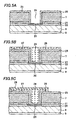
- Figs. 3 to 7 are cross-sectional views showing process steps applied to the object chucked in the manner shown in Fig. 2.
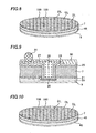
- Fig. 9 is a cross-sectional view showing process steps applied to the object chucked in the manner shown in Figs. 8.
- First, a conductive film used in an embodiment of the invention will be described as an example of a conductive member with reference to figures. Figs. 1A, 1B, and 1C are cross-sectional views showing a structure of the conductive film.
- A
conductive film 9 shown in Fig. 1A is formed of aprotection layer 1, aconductive layer 2, anattachment layer 3, and aseparation layer 4 laminated in this order. Alternatively, theconductive film 9 is formed of theprotection layer 1, theconductive layer 2, apolyimide layer 5, theattachment layer 3, and theseparation layer 4 laminated in this order. Theprotection layer 1 is a plastic film formed of a plastic material such as polyethylene, polypropylene, polyvinyl chloride, polystyrene, polyethylene terephthalate, polyacrylonitrile, or the like. Theconductive layer 2 is formed of a conductive polymer containing conjugated double bonds in its molecular structure, such as polypyrrole or the like. Theattachment layer 3 is formed of an adhesive such as an acrylic type adhesive, a urethane type adhesive, a synthetic rubber type adhesive, or the like. Theseparation layer 4 is a release paper or the like, and separated when theconductive film 9 is used. - The
conductive film 9A shown in Fig. 1B is formed of theprotection layer 1, thepolyimide layer 5, theconductive layer 2, theattachment layer 3, and theseparation layer 4 laminated in this order. Since polyimide has high thermal resistance, using the conductive film having such high thermal resistance can provide stable chucking characteristics even at high temperature. - The
conductive film 9B shown in Fig. 1C is formed of theprotection layer 1, apolymer layer 6 formed by polymerizing a conductive material and polyimide, theattachment layer 3, and theseparation layer 4 laminated in this order. Theattachment layer 3 in Figs. 1B and 1C is preferably formed of a material having thermal resistance. - Next, an chucking of the embodiment of the invention using the described
conductive films conductive film 9 hereafter, but the methods are the same even using theconductive films - As shown in Fig. 2, a
layered body 15 includes asemiconductor substrate 7 and aglass substrate 8 for supporting thesemiconductor substrate 7. Thelayered body 15 is the object to be chucked. It is noted that electronic devices are formed on the surface of thesemiconductor substrate 7. Theseparation layer 4 of theconductive film 9 is separated and removed to expose theattachment layer 3, so that theconductive film 9 is attached to theglass substrate 8 with thisattachment layer 3 therebetween. Thelayered body 15 forms a shape of a disk-like semiconductor wafer. Thesemiconductor substrate 7 has a large number of semiconductor integratedcircuits 100 sectioned in a matrix by a dicing line DL. Although theglass substrate 8 is used as a supporting body of thesemiconductor substrate 7, the other insulator of a ceramic, quartz, a plastic, or a resin, e.g., a resist or an epoxy resin, can be used as the supporting body. - Then, as shown in Fig. 3, the
layered body 15 attached with theconductive film 9 is set on astage 10 set in avacuum chamber 12 of a dry-etching apparatus or the like. At this time, the surface of thestage 10 is covered with a dielectric layer (not shown). Apower supply 13 is to supply a DC voltage or an AC voltage to an internal electrode, and anAC power supply 14 is to supply an AC voltage to thestage 10. - Then, after the
layered body 15 is set on thestage 10, a voltage is applied to aninternal electrode 11 provided in thestage 10 to generate positive and negative electric charges on the surfaces of theconductive film 9 and thestage 10, and thelayered body 15 is chucked on thestage 10 with static electricity generated therebetween. Then, thesemiconductor substrate 7 of the chuckedlayered body 15 is processed by dry-etching, CVD (chemical vapor deposition), or PVD (physical vapor deposition), in a vacuum state. - Next, the processing of the described
layered body 15 will be described in detail. Figs. 4A to 6 are partial cross-sectional views of thelayered body 15 in process order. First, as shown in Fig. 4A, apad electrode 20 as well as electronic devices (not shown) (e.g. a CCD (Charge Coupled Device), a light receiving element such as an infrared ray sensor, or a light emissive element) is formed on a front surface of thesemiconductor substrate 7, thepad electrode 20 being connected with these electronic devices. Thepad electrode 20 is formed on the front surface of thesemiconductor substrate 7 with aninterlayer insulation film 21 therebetween. - The
semiconductor substrate 7 is formed of, for example, silicon (Si), and preferably has a thickness of about 20 to 200 µm. Thepad electrode 20 is formed of, for example, aluminum (Al), and preferably has a thickness of about 1 µm. It is noted that a passivation film (not shown) is formed on thesemiconductor substrate 7, covering at least a part of thepad electrode 20. Theinterlayer insulation film 21 is formed of, for example, an oxide film, and preferably has a thickness of about 0.8 µm. Then, theglass substrate 8 having a thickness of about 80 to 100 µm is attached on the front surface of thesemiconductor substrate 7 with aresin layer 22 therebetween. Theconductive film 9 is then attached to the front surface of theglass substrate 8. - Next, as shown in Fig. 4B, a resist
layer 23 is selectively formed on a back surface of thesemiconductor substrate 7. Then, thelayered body 15 formed with the resistlayer 23 and attached with theconductive film 9 is set on thestage 10 in thevacuum chamber 12 of the dry-etching apparatus, with theconductive film 9 opposed to thestage 10. Then, thelayered body 15 thus set is electrostatically chucked thereon, and thesemiconductor substrate 7 is dry-etched. As etching gas for the dry-etching, CHF3 or the like can be used, for example. A viahole 24 is formed by this dry-etching, penetrating thesemiconductor substrate 7 and theinterlayer insulation film 21 in a position corresponding to thepad electrode 20. - Next, after the resist
layer 23 is removed, as shown in Fig. 4C, aninsulation film 25 is formed on the whole back surface of thesemiconductor substrate 7 including in the viahole 24 by a CVD (chemical vapor deposition) method. Theinsulation film 25 is formed of, for example, a silicon oxide film (SiO2 film) or a silicon nitride film (SiN film), and formed by a plasma CVD apparatus of an electrostatic chuck type. - Next, as shown in Fig. 5A, a resist layer (not shown) is formed on the
insulation film 25, and theinsulation film 25 at a bottom of the viahole 24 is dry-etched and removed using the resist layer as a mask. In this dry-etching process, too, thelayered body 15 can be electrostatically chucked in the same manner as described above. - Next, as shown in Fig. 5B, a
barrier metal layer 26 is formed on theinsulation film 25 on the back surface of thesemiconductor substrate 7 including in the viahole 24. Furthermore, a seed layer (not shown) is formed on thebarrier metal layer 26. Thebarrier metal layer 26 is formed of metal, for example, a titanium tungsten (TiW) layer, a titanium nitride (TiN) layer, a tantalum nitride (TaN) layer, or the like. The seed layer (not shown) is to be an electrode for forming awiring layer 27 by plating, which will be described below, and formed of, for example, copper (Cu). Thebarrier metal layer 26 can be formed by a PVD (physical vapor deposition) method, and at this time thelayered body 15 can be electrostatically chucked in a PVD apparatus in the same manner as described above. - Next, a penetrating
electrode 28 formed of copper (Cu) and awiring layer 27 continued and connected to the penetratingelectrode 28 are formed on thebarrier metal layer 26 and the seed layer (not shown) including in the viahole 24 by an electrolytic plating method, for example. The penetratingelectrode 28 and thewiring layer 27 are electrically connected with thepad electrode 20 exposed at the bottom of the viahole 24 with thebarrier metal layer 26 and the seed layer (not shown) therebetween. - Next, as shown in Fig. 5C, a resist
layer 29 for patterning thewiring layer 27 in a predetermined pattern is selectively formed on thewiring layer 27 on the back surface of thesemiconductor substrate 7. Then, an unnecessary portion of thewiring layer 27 and the seed layer (not shown) is etched and removed using the resistlayer 29 as a mask. Then, thebarrier metal layer 26 is etched and removed using thewiring layer 27 as a mask. When these etching processes are performed by a dry-etching method, thelayered body 15 can be electrostatically chucked in the dry-etching apparatus in the same manner as described above. - Next, as shown in Fig. 6, a
protection layer 30 formed of, for example, a resist material such as a solder resist is formed on the back surface of thesemiconductor substrate 7 so as to cover thesubstrate 7. An opening is formed in theprotection layer 30 in a position corresponding to thewiring layer 27. Then, a ball-shaped conductive terminal 31 formed of, for example, metal such as solder is formed on thewiring layer 27 exposed in the opening by a screen printing method. It is noted that the invention can be applied to a semiconductor device that does not have theconductive terminal 31, that is, a so-called LGA (land grid array) type semiconductor device. - Then, this
layered body 15 is diced along a dicing line DL, and separated into individual dies. Theconductive film 9 is separated and removed from the layeredbody 15 before or after this dicing process. As described above, in the method described above it is possible to use the electrostatic chucking for all the steps to be performed in a vacuum state such as the dry-etching, CVD (chemical vapor deposition), PVD (physical vapor deposition) processes usually performed in a manufacturing process of a semiconductor device having an insulator such as theglass substrate 8. This can provide uniformity of the temperature distribution and prevent thelayered body 15 warping, thereby enhancing the yield. - Furthermore, although the electrostatic chucking is performed to the
layered body 15 of thesemiconductor substrate 7 and theglass substrate 8 in the embodiment, the embodiment can be similarly applied to theinsulator 50 formed of glass, a ceramic, quartz, a plastic, a resin, e.g., a resist or an epoxy resin, or the like as shown in Fig. 7. That is, theconductive film 9 is attached on a surface of theinsulator 50, and theinsulator 50 is electrostatically chucked on thestage 10 set in thevacuum chamber 12 of the dry-etching apparatus or the like as shown in Fig. 3, with theconductive film 9 being opposed to thestage 10. Then, thisinsulator 50 is processed by dry-etching, CVD (chemical vapor deposition), or PVD (physical vapor deposition) in a vacuum state, while being electrostatically chucked. - Furthermore, although the
conductive film 9 is provided on the surface of theglass substrate 8 or theinsulator 50 formed of a ceramic, quartz, a plastic, a resin or the like in the described embodiment, it is possible, as shown in Fig. 8, that theconductive film 9 is provided on aninsulation film 40, e.g., a silicon oxide film, a silicon nitride film or a resin layer, formed on thesemiconductor substrate 7 and electrostatically chucked in the similar manner, and processes such as dry-etching, CVD, or PVD are performed to thesemiconductor substrate 7. - In detail, as shown in Fig. 9, the
conductive film 9 is directly provided on apassivation film 55 as theinsulation film 40 formed on the surface of thesemiconductor substrate 7 and electrostatically chucked, and various processes in the semiconductor manufacturing process can be performed to this assembly. This case has an advantage that thesemiconductor substrate 7 can be chucked with static electricity more firmly and processing accuracy can be enhanced. This is effective particularly in the case of thethick insulation film 40. Furthermore, theconductive film 9 functions as a support body such as theglass substrate 8, so that there is an advantage that the required semiconductor device can be manufactured without using the support body such as theglass substrate 8. Since the other structure in Fig. 9 is the same as in Fig. 6, the same numerals are provided and the description is omitted. - The above description is made with the
conductive film 9, but the other conductive member can be used and also has the similar effect in electrostatic chucking. That is, a conductive resin is prepared by mixing a resin, such as a resist or an epoxy resin, and the same conductive material as the conductive material of theconductive film 9, and aconductive resin layer 45 is formed on the surface of an insulation substrate formed of a glass, a ceramic, quartz, or a plastic or the surface of theinsulation film 40 formed on the surface of thesemiconductor substrate 7, as shown in Fig. 10, using the conductive resin. Then, the insulation substrate or thesemiconductor substrate 7 is electrostatically chucked in the similar manner, and the processes are performed to this assembly. In this case, theconductive resin layer 45 can be used as a support body such as theglass substrate 8. Theconductive resin layer 45 is to be separated and removed like theconductive film 9 after the insulation substrate or thesemiconductor substrate 7 is processed.
Claims (28)
- A method of chucking, comprising:- providing an object (15) comprising a surface portion that is made of an insulator;- attaching a member (9) comprising a conductive layer (2) to the surface portion;- placing the object to which the member is attached in a vacuum chamber (12); and- chucking the object to a stage (10) provided in the vacuum chamber (12) by generating electrostatic charges between the member and the stage (10).
- The method of claim 1, wherein the insulator comprises a glass, a ceramic, quartz, a plastic, or a resin.
- The method of claim 1 or 2, wherein the member (9) further comprises a protection layer (1) and an adhesive layer (3).
- The method of claim 1 or 2, wherein the member (9) further comprises a protection layer (1), a polyimide layer (5) and an adhesive layer (3).
- The method of claim 1 or 2, wherein the member (9). further comprises a protection layer (1), a polymer layer (6) formed by polymerizing a conductive material and polyimide, and an adhesive layer (3).
- The method of claim 1, wherein the member (9) comprises a conductive resin layer (22).
- A method of chucking, comprising:- providing an object (15) for chucking;- attaching a substrate (8) made of an insulator to the object;- attaching a member (9) comprising a conductive layer (2) to the substrate (8);- placing the object to which the member and the substrate (8) are attached in a vacuum chamber (12); and- chucking the object (15) to a stage (10) provided in the vacuum chamber (12) by generating electrostatic charges between the member (9) and the stage (10).
- The method of claim 7, wherein the insulator comprises a glass, a ceramic, quartz, a plastic, or a resin.
- The method of claim 7 or 8, wherein the member (9) further comprises a protection layer (1) and an adhesive layer (3).
- The method of claim 7 or 8, wherein the member (9) further comprises a protection layer (1), a polyimide layer (5) and an adhesive (3) layer.
- The method of claim 7 or 8, wherein the member (9) further comprises a protection layer (1), a polymer layer (6) formed by polymerizing a conductive material and polyimide, and an adhesive layer (3).
- The method of claim 7 or 8, wherein the object (15) comprises a semiconductor wafer (7), an insulator or a conductor.
- The method of claim 7, wherein the member (9) comprises a conductive resin layer (45).
- A method of processing objects, comprising:- providing an object (15) comprising a surface portion that is made of an insulator;- attaching a member (9) comprising a conductive layer (2) to the surface portion;- placing the object (15) to which the member (9) is attached in a vacuum chamber (12);- chucking the object (15) to a stage (10) provided in the vacuum chamber (12) by generating electrostatic charges between the member (9) and the stage (10); and- processing the object chucked to the stage (10) in the vacuum chamber (12).
- The method of claim 14, wherein the insulator comprises a glass, a ceramic, quartz, a plastic, or a resin.
- The method of claim 14 or 15, wherein the processing of the chucked object (15) comprises a dry-etching, a chemical vapor deposition or physical vapor deposition.
- The method according to any of claims 14 to 16, wherein the member (9) further comprises a protection layer (1) and an adhesive layer (3).
- The method according to any of claims 14 to 16, wherein the member (9) further comprises a protection layer (1), a polyimide layer (5) and an adhesive layer (3).
- The method according to any of claims 14 to 16, wherein the member (9) further comprises a protection layer (1), a polymer layer (6) formed by polymerizing a conductive material and polyimide, and an adhesive layer (3).
- The method according to any of claims 14 to 19, wherein the member (9) comprises a conductive resin layer (45).
- A method of processing an object, comprising:attaching a substrate (8) made of an insulator to the object (15);- attaching a member (9) comprising a conductive layer (2) to the substrate (8);- placing the object (15) to which the member (9) and the substrate (8) are attached in a vacuum chamber (12);- chucking the object (15) to a stage (10) provided in the vacuum chamber (12) by generating electrostatic charges between the member (10) and the stage (12); and- processing the object chucked to the stage (10) in the vacuum chamber (12).
- The method of claim 21, wherein the insulator comprises a glass, a ceramic, quartz, a plastic, or a resin.
- The method of claim 21 or 22, wherein the processing of the chucked object (15) comprises a dry-etching, a chemical vapor deposition or physical vapor deposition.
- The method according to any of claims 21 to 23, wherein the member (9) further comprises a protection layer (1) and an adhesive layer (3).
- The method according to any of claims 21 to 23, wherein the member (9) further comprises a protection layer (1), a polyimide layer (5) and an adhesive layer (3).
- The method according to any of claims 21 to 23, wherein the member (9) further comprises a protection layer (1), a polymer layer (5) formed by polymerizing a conductive material and polyimide, and an adhesive layer (3).
- The method according to any of claims 21 to 26, wherein the object (15) comprises a semiconductor wafer (7), an insulator or a conductor.
- The method according to any of claims 21 to 27, wherein the member (9) comprises a conductive resin layer (45).
Applications Claiming Priority (1)
| Application Number | Priority Date | Filing Date | Title |
|---|---|---|---|
| JP2004345275 | 2004-11-30 |
Publications (3)
| Publication Number | Publication Date |
|---|---|
| EP1662559A2 true EP1662559A2 (en) | 2006-05-31 |
| EP1662559A3 EP1662559A3 (en) | 2007-12-19 |
| EP1662559B1 EP1662559B1 (en) | 2011-01-05 |
Family
ID=35559482
Family Applications (1)
| Application Number | Title | Priority Date | Filing Date |
|---|---|---|---|
| EP05026071A Expired - Lifetime EP1662559B1 (en) | 2004-11-30 | 2005-11-30 | Method of processing objects comprising a surface portion made of an insulator |
Country Status (6)
| Country | Link |
|---|---|
| US (1) | US7495881B2 (en) |
| EP (1) | EP1662559B1 (en) |
| KR (1) | KR100731244B1 (en) |
| CN (1) | CN1790889B (en) |
| DE (1) | DE602005025722D1 (en) |
| TW (1) | TWI271815B (en) |
Cited By (2)
| Publication number | Priority date | Publication date | Assignee | Title |
|---|---|---|---|---|
| WO2007110191A1 (en) * | 2006-03-23 | 2007-10-04 | Fraunhofer-Gesellschaft zur Förderung der angewandten Forschung e.V. | Method and device for electrostatically fixing substrates having a conductive layer |
| US7733624B2 (en) | 2006-03-23 | 2010-06-08 | Fraunhofer-Gesellschaft Zur Foerderung Der Angewandten Forschung E.V. | Method and device for electrostatic fixing of substrates with polarized molecules |
Families Citing this family (12)
| Publication number | Priority date | Publication date | Assignee | Title |
|---|---|---|---|---|
| JP2010210590A (en) * | 2009-03-12 | 2010-09-24 | Fujifilm Corp | Radiation detector |
| WO2012018013A1 (en) * | 2010-08-06 | 2012-02-09 | 旭硝子株式会社 | Support substrate |
| US9030797B2 (en) * | 2012-06-01 | 2015-05-12 | Infineon Technologies Ag | Thin substrate electrostatic chuck system and method |
| JP6149786B2 (en) * | 2014-04-11 | 2017-06-21 | 豊田合成株式会社 | Semiconductor device and manufacturing method of semiconductor device |
| CN107958866B (en) * | 2015-11-20 | 2021-09-14 | 苏州赛森电子科技有限公司 | Wafer fixing device in evaporation coating process |
| KR102391997B1 (en) * | 2016-06-24 | 2022-04-28 | 큐로미스, 인크 | Polycrystalline ceramic substrate and manufacturing method thereof |
| US20180025931A1 (en) * | 2016-07-22 | 2018-01-25 | Applied Materials, Inc. | Processed wafer as top plate of a workpiece carrier in semiconductor and mechanical processing |
| CN106910703B (en) * | 2017-03-10 | 2020-12-01 | 京东方科技集团股份有限公司 | Stage and method of making the same, processing device and method of operating the same |
| CN108231655B (en) * | 2018-01-12 | 2020-06-16 | 上海华虹宏力半导体制造有限公司 | Method for electrostatically attracting a substrate |
| JP6583897B1 (en) * | 2018-05-25 | 2019-10-02 | ▲らん▼海精研股▲ふん▼有限公司 | Method for manufacturing ceramic electrostatic chuck |
| CN109738481A (en) * | 2018-11-27 | 2019-05-10 | 武汉嘉仪通科技有限公司 | A kind of the Seebeck coefficient measuring device and method of thin-film material |
| KR102906230B1 (en) * | 2022-04-14 | 2026-01-05 | 엔테그리스, 아이엔씨. | Conductive polymer layer for charge dissipation |
Citations (4)
| Publication number | Priority date | Publication date | Assignee | Title |
|---|---|---|---|---|
| JPS62275137A (en) | 1985-11-05 | 1987-11-30 | Achilles Corp | Preparation of conductive composite |
| JPH0563062A (en) | 1991-08-30 | 1993-03-12 | Toto Ltd | Electrostatic chuck |
| JPH05331431A (en) | 1992-05-28 | 1993-12-14 | Achilles Corp | Conductive transparent protective film |
| JPH10206876A (en) | 1997-01-20 | 1998-08-07 | Sharp Corp | LCD display substrate |
Family Cites Families (10)
| Publication number | Priority date | Publication date | Assignee | Title |
|---|---|---|---|---|
| US5838529A (en) | 1995-12-22 | 1998-11-17 | Lam Research Corporation | Low voltage electrostatic clamp for substrates such as dielectric substrates |
| JP3805134B2 (en) | 1999-05-25 | 2006-08-02 | 東陶機器株式会社 | Electrostatic chuck for insulating substrate adsorption |
| JP2002305234A (en) | 2001-04-05 | 2002-10-18 | Matsushita Electric Ind Co Ltd | Silicon wafer backside etching method and silicon wafer protection tape |
| US6693790B2 (en) * | 2001-04-12 | 2004-02-17 | Komatsu, Ltd. | Static electricity chuck apparatus and semiconductor producing apparatus provided with the static electricity chuck apparatus |
| JP2003224180A (en) * | 2002-01-28 | 2003-08-08 | Kyocera Corp | Wafer support member |
| US7102726B2 (en) * | 2002-03-15 | 2006-09-05 | Lg. Philips Lcd Co., Ltd. | System for fabricating liquid crystal display and method of fabricating liquid crystal display using the same |
| EP1359466A1 (en) * | 2002-05-01 | 2003-11-05 | ASML Netherlands B.V. | Chuck, lithographic projection apparatus, method of manufacturing a chuck and device manufacturing method |
| US7092231B2 (en) * | 2002-08-23 | 2006-08-15 | Asml Netherlands B.V. | Chuck, lithographic apparatus and device manufacturing method |
| JP2004140056A (en) * | 2002-10-16 | 2004-05-13 | Nok Corp | Electrostatic chuck |
| JP4130167B2 (en) * | 2003-10-06 | 2008-08-06 | 日東電工株式会社 | Semiconductor wafer peeling method |
-
2005
- 2005-10-14 TW TW094135825A patent/TWI271815B/en not_active IP Right Cessation
- 2005-11-25 CN CN2005101268969A patent/CN1790889B/en not_active Expired - Fee Related
- 2005-11-28 US US11/287,484 patent/US7495881B2/en not_active Expired - Lifetime
- 2005-11-29 KR KR1020050114695A patent/KR100731244B1/en not_active Expired - Fee Related
- 2005-11-30 DE DE602005025722T patent/DE602005025722D1/en not_active Expired - Lifetime
- 2005-11-30 EP EP05026071A patent/EP1662559B1/en not_active Expired - Lifetime
Patent Citations (4)
| Publication number | Priority date | Publication date | Assignee | Title |
|---|---|---|---|---|
| JPS62275137A (en) | 1985-11-05 | 1987-11-30 | Achilles Corp | Preparation of conductive composite |
| JPH0563062A (en) | 1991-08-30 | 1993-03-12 | Toto Ltd | Electrostatic chuck |
| JPH05331431A (en) | 1992-05-28 | 1993-12-14 | Achilles Corp | Conductive transparent protective film |
| JPH10206876A (en) | 1997-01-20 | 1998-08-07 | Sharp Corp | LCD display substrate |
Cited By (2)
| Publication number | Priority date | Publication date | Assignee | Title |
|---|---|---|---|---|
| WO2007110191A1 (en) * | 2006-03-23 | 2007-10-04 | Fraunhofer-Gesellschaft zur Förderung der angewandten Forschung e.V. | Method and device for electrostatically fixing substrates having a conductive layer |
| US7733624B2 (en) | 2006-03-23 | 2010-06-08 | Fraunhofer-Gesellschaft Zur Foerderung Der Angewandten Forschung E.V. | Method and device for electrostatic fixing of substrates with polarized molecules |
Also Published As
| Publication number | Publication date |
|---|---|
| KR20060060600A (en) | 2006-06-05 |
| CN1790889B (en) | 2010-12-08 |
| CN1790889A (en) | 2006-06-21 |
| KR100731244B1 (en) | 2007-06-22 |
| US20060120010A1 (en) | 2006-06-08 |
| US7495881B2 (en) | 2009-02-24 |
| DE602005025722D1 (en) | 2011-02-17 |
| TWI271815B (en) | 2007-01-21 |
| EP1662559A3 (en) | 2007-12-19 |
| TW200620528A (en) | 2006-06-16 |
| EP1662559B1 (en) | 2011-01-05 |
Similar Documents
| Publication | Publication Date | Title |
|---|---|---|
| EP1662559B1 (en) | Method of processing objects comprising a surface portion made of an insulator | |
| CN101114592B (en) | Semiconductor device and method of manufacturing the same | |
| US10943853B2 (en) | Semiconductor device and manufacturing method thereof | |
| TWI251314B (en) | Manufacturing method of semiconductor device, semiconductor device, circuit substrate and electronic equipment | |
| EP1489658B1 (en) | Method for manufacturing semiconductor package | |
| CN213366557U (en) | Multilayer electrostatic chuck assembly | |
| US10811339B2 (en) | Semiconductor device and manufacturing method thereof | |
| TW201308559A (en) | Substrate, infrared sensor, and through electrode forming method | |
| US20080237819A1 (en) | Bipolar Carrier Wafer and Mobile Bipolar Electrostatic Wafer Arrangement | |
| US10032670B2 (en) | Plasma dicing of silicon carbide | |
| US20110037161A1 (en) | Electrostatic chucking of an insulator handle substrate | |
| TW201001645A (en) | Semiconductor device and method of manufacturing the same | |
| CN101996858B (en) | Manufacturing method of semiconductor device | |
| JP4898199B2 (en) | Manufacturing method of semiconductor device | |
| US10068789B2 (en) | Method of using a wafer cassette to charge an electrostatic carrier | |
| US8278738B2 (en) | Method of producing semiconductor device and semiconductor device | |
| CN111613563A (en) | A kind of electrostatic chuck and wafer testing method | |
| JP2004221134A (en) | Semiconductor device manufacturing apparatus and semiconductor device manufacturing method | |
| CN110875232A (en) | Wafer level packaging method and packaging structure | |
| JP2006080509A (en) | Thin substrate support | |
| JP2836986B2 (en) | Electrostatic chuck and method of manufacturing the same | |
| US7307010B2 (en) | Method for processing a thin semiconductor substrate | |
| JP2003266354A (en) | Vacuum chuck | |
| US20250145514A1 (en) | Electrostatic clamping of electrically insulating substrates | |
| JPH07321186A (en) | Electrostatic adsorption device |
Legal Events
| Date | Code | Title | Description |
|---|---|---|---|
| PUAI | Public reference made under article 153(3) epc to a published international application that has entered the european phase |
Free format text: ORIGINAL CODE: 0009012 |
|
| AK | Designated contracting states |
Kind code of ref document: A2 Designated state(s): AT BE BG CH CY CZ DE DK EE ES FI FR GB GR HU IE IS IT LI LT LU LV MC NL PL PT RO SE SI SK TR |
|
| AX | Request for extension of the european patent |
Extension state: AL BA HR MK YU |
|
| PUAL | Search report despatched |
Free format text: ORIGINAL CODE: 0009013 |
|
| AK | Designated contracting states |
Kind code of ref document: A3 Designated state(s): AT BE BG CH CY CZ DE DK EE ES FI FR GB GR HU IE IS IT LI LT LU LV MC NL PL PT RO SE SI SK TR |
|
| AX | Request for extension of the european patent |
Extension state: AL BA HR MK YU |
|
| 17P | Request for examination filed |
Effective date: 20080523 |
|
| 17Q | First examination report despatched |
Effective date: 20080626 |
|
| AKX | Designation fees paid |
Designated state(s): DE FI FR GB |
|
| RTI1 | Title (correction) |
Free format text: METHOD OF PROCESSING OBJECTS COMPRISING A SURFACE PORTION MADE OF AN INSULATOR |
|
| GRAP | Despatch of communication of intention to grant a patent |
Free format text: ORIGINAL CODE: EPIDOSNIGR1 |
|
| RAP1 | Party data changed (applicant data changed or rights of an application transferred) |
Owner name: KANTO SANYO SEMICONDUCTORS CO., LTD. Owner name: SANYO ELECTRIC CO., LTD. |
|
| GRAS | Grant fee paid |
Free format text: ORIGINAL CODE: EPIDOSNIGR3 |
|
| GRAA | (expected) grant |
Free format text: ORIGINAL CODE: 0009210 |
|
| AK | Designated contracting states |
Kind code of ref document: B1 Designated state(s): DE FI FR GB |
|
| REG | Reference to a national code |
Ref country code: GB Ref legal event code: FG4D |
|
| REF | Corresponds to: |
Ref document number: 602005025722 Country of ref document: DE Date of ref document: 20110217 Kind code of ref document: P |
|
| REG | Reference to a national code |
Ref country code: DE Ref legal event code: R096 Ref document number: 602005025722 Country of ref document: DE Effective date: 20110217 |
|
| PG25 | Lapsed in a contracting state [announced via postgrant information from national office to epo] |
Ref country code: FI Free format text: LAPSE BECAUSE OF FAILURE TO SUBMIT A TRANSLATION OF THE DESCRIPTION OR TO PAY THE FEE WITHIN THE PRESCRIBED TIME-LIMIT Effective date: 20110105 |
|
| PLBE | No opposition filed within time limit |
Free format text: ORIGINAL CODE: 0009261 |
|
| STAA | Information on the status of an ep patent application or granted ep patent |
Free format text: STATUS: NO OPPOSITION FILED WITHIN TIME LIMIT |
|
| 26N | No opposition filed |
Effective date: 20111006 |
|
| REG | Reference to a national code |
Ref country code: DE Ref legal event code: R097 Ref document number: 602005025722 Country of ref document: DE Effective date: 20111006 |
|
| PGFP | Annual fee paid to national office [announced via postgrant information from national office to epo] |
Ref country code: GB Payment date: 20131126 Year of fee payment: 9 Ref country code: FR Payment date: 20131025 Year of fee payment: 9 Ref country code: DE Payment date: 20131129 Year of fee payment: 9 |
|
| REG | Reference to a national code |
Ref country code: DE Ref legal event code: R119 Ref document number: 602005025722 Country of ref document: DE |
|
| GBPC | Gb: european patent ceased through non-payment of renewal fee |
Effective date: 20141130 |
|
| REG | Reference to a national code |
Ref country code: FR Ref legal event code: ST Effective date: 20150731 |
|
| PG25 | Lapsed in a contracting state [announced via postgrant information from national office to epo] |
Ref country code: DE Free format text: LAPSE BECAUSE OF NON-PAYMENT OF DUE FEES Effective date: 20150602 Ref country code: GB Free format text: LAPSE BECAUSE OF NON-PAYMENT OF DUE FEES Effective date: 20141130 |
|
| PG25 | Lapsed in a contracting state [announced via postgrant information from national office to epo] |
Ref country code: FR Free format text: LAPSE BECAUSE OF NON-PAYMENT OF DUE FEES Effective date: 20141201 |