EP1662550A1 - Method for producing soi wafer - Google Patents
Method for producing soi wafer Download PDFInfo
- Publication number
- EP1662550A1 EP1662550A1 EP04772682A EP04772682A EP1662550A1 EP 1662550 A1 EP1662550 A1 EP 1662550A1 EP 04772682 A EP04772682 A EP 04772682A EP 04772682 A EP04772682 A EP 04772682A EP 1662550 A1 EP1662550 A1 EP 1662550A1
- Authority
- EP
- European Patent Office
- Prior art keywords
- wafer
- cleavage
- bonded
- ion
- bonded wafer
- Prior art date
- Legal status (The legal status is an assumption and is not a legal conclusion. Google has not performed a legal analysis and makes no representation as to the accuracy of the status listed.)
- Granted
Links
Images

Classifications
-
- H—ELECTRICITY
- H10—SEMICONDUCTOR DEVICES; ELECTRIC SOLID-STATE DEVICES NOT OTHERWISE PROVIDED FOR
- H10P—GENERIC PROCESSES OR APPARATUS FOR THE MANUFACTURE OR TREATMENT OF DEVICES COVERED BY CLASS H10
- H10P90/00—Preparation of wafers not covered by a single main group of this subclass, e.g. wafer reinforcement
- H10P90/19—Preparing inhomogeneous wafers
- H10P90/1904—Preparing vertically inhomogeneous wafers
- H10P90/1906—Preparing SOI wafers
- H10P90/1914—Preparing SOI wafers using bonding
- H10P90/1916—Preparing SOI wafers using bonding with separation or delamination along an ion implanted layer, e.g. Smart-cut
-
- H—ELECTRICITY
- H10—SEMICONDUCTOR DEVICES; ELECTRIC SOLID-STATE DEVICES NOT OTHERWISE PROVIDED FOR
- H10W—GENERIC PACKAGES, INTERCONNECTIONS, CONNECTORS OR OTHER CONSTRUCTIONAL DETAILS OF DEVICES COVERED BY CLASS H10
- H10W10/00—Isolation regions in semiconductor bodies between components of integrated devices
- H10W10/10—Isolation regions comprising dielectric materials
- H10W10/181—Semiconductor-on-insulator [SOI] isolation regions, e.g. buried oxide regions of SOI wafers
Definitions
- the present invention relates to a method for producing an SOI wafer, and more particularly to a method for producing an SOI wafer in combination with a cleavage method comprising a hydrogen ion-implantation.
- An SOI wafer has been used in an LSI of high-speed low-power consumption, as it is considered superior to a conventional silicon wafer in some properties, including separation between devices, reduced parasitic capacity between a device and a substrate and a three-dimensional structure to be feasible.
- One of methods for producing the SOI wafer in the prior art includes the smart cut method in which hydrogen ion is implanted into a silicon wafer surface and then the silicon wafer is bonded to another wafer, and subsequently thus obtained bonded wafer is subjected to a heat treatment for cleavage so as for a part of the silicon wafer to be cleaved and separated away at the site of ion-implanted layer serving as an interface layer.
- the wafer for an active layer that has been implanted with the hydrogen ion from the silicon wafer surface is bonded with the supporting wafer. Consequently, a bonded wafer having an insulating layer in the site of bonding interface is formed.
- a heat treatment for cleavage As for a set temperature used in the heat treatment for cleavage, as disclosed in Patent Document 1, for example, the heat treatment has to be carried out at approximately 500°C or higher.
- a first invention provides a method for producing an SOI wafer, comprising the steps of:
- the ion-implanted layer is formed in the active layer wafer (e.g. , a wafer comprising an oxide film formed on top of a silicon wafer). Subsequently, this active layer wafer is bonded with the supporting wafer (e.g., a silicon wafer) via the insulating film interposed therebetween. This bonding process of the active layer wafer with the supporting wafer consequently produces a bonded wafer with the intervention of the insulating film at the site of bonding surface. After this step of processing, the bonded wafer is heat treated at the set temperature (e.g. , temperature in a range of 400°C to 1000°C).
- the set temperature e.g. , temperature in a range of 400°C to 1000°C.
- the temperature variation within the surface of the bonded wafer has been controlled within 40°C. Accordingly, bubbles of noble gas are formed in the ion-implanted layer, and the cleavage occurs at the site of ion-implanted layer as the interface.
- the temperature within the surface of the bonded wafer has been held substantially uniform, it hardly produces any regions that will be left without occurrence of cleavage but a complete cleavage would be induced over the entire surface of the bonded wafer at the site of ion-implanted layer as the interface.
- the temperature variation within the surface of the bonded wafer during the heat treatment for cleavage is controlled within 40°C.
- the cleavage takes effect in a region in the surface of the bonded wafer where the temperature is in a range of 410°C to 450°C.
- the wafer is forced to be cleaved and separated at the site of bonding interface specifically in a region at the temperature of 400°C. Consequently, the SOI wafer partially lacking the SOI structure would be produced.
- a heat treatment device used to provide the heat treatment for cleavage is an RTP (Rapid Thermal Processing) furnace of single wafer processing type. This is because the bonded wafer can be heated rapidly and uniformly by applying lamp heating to the wafers one by one in the single wafer processing type of furnace.
- RTP Rapid Thermal Processing
- the rate of temperature increase to the cleavage starting temperature should be controlled to be 20°C/min, for example, for carrying out the heat treatment for cleavage.
- the rate of temperature increase over 20°C/min, there will be a local region within the wafer surface that is not able to follow the temperature increase. This may cause uneven temperature distribution across the wafer surface. Accordingly, if the rate of temperature increase is set to be 20°C /min or lower, the temperature variation over the entire surface of the bonded wafer can be controlled within 40°C easily and accurately.
- a second invention provides a method for producing an SOI wafer as defined in the first invention, in which the set temperature is in a range of 400°C to 1000°C.
- the set temperature for the heat treatment for cleavage of the bonded wafer has employed a range of 400°C to 1000°C .
- the set temperature below 400°C may be associated with a problem that the cleavage starting temperature of the bonded wafer would not be reached, failing in inducing the cleavage. With the temperature over 1000°C, such a problem may occur that a reaction tube (silica tube) of the heat treatment device could be deformed.
- a reaction tube silicon tube
- the entire surface of the bonded wafer should be in a temperature range of 400°C to 1000°C and that the temperature variation within the surface should be 40°C in maximum.
- the temperature within the furnace during the introduction is required to be suppressed to 400°C or lower, and if taking the throughput in production of the SOI wafer into account, preferably the temperature within the furnace during the introduction is in a range of 300°C to 400°C. That is, the bonded wafer can be heated while keeping the small temperature variation within the surface of the bonded wafer by setting the introduction temperature at 400°C or lower.
- a third invention provides a method for producing an SOI wafer as defined in the second invention, in which the heat treatment is performed while holding the bonded wafer substantially vertical so as to induce the cleavage in the bonded wafer at the site of ion-implanted layer as the interface.
- a heat source for heating the bonded wafer while holding the bonded wafer substantially vertical is disposed in proximal to the top and the back surfaces of the bonded wafer.
- the heat source may employ an infrared lamp, for example.
- the bonded wafer is held vertical by a supporting jig made of silica disposed in a reaction chamber within the RTP furnace. Then, this bonded wafer is heat treated by the infrared lamp disposed laterally with respect to the top and the back surfaces of the bonded wafer. The reason why the bonded wafer is held vertical is to prevent the cleaved and separated wafers after the heat treatment for cleavage from coming into contact with each other again. Then, the entire surface of this bonded wafer is heated uniformly and rapidly to thereby make the temperature within the surface of the bonded wafer substantially uniform. Thus, the complete cleavage can be achieved across the entire surface of the bonded wafer at the site of the ion-implanted layer as the interface.
- a bonded wafer is heat treated at a set temperature in a range of 400°C to 1000°C.
- a temperature variation within the surface of the bonded wafer is controlled to be within 40°C. Consequently, bubbles of noble gas are formed in an ion-implanted layer, and the bonded wafer is cleaved and separated (i.e., a part of the active layer wafer is separated from the remaining part of the SOI wafer) at the site of the ion-implanted layer specifically in a region containing thus formed bubbles as the interface.
- the temperature within the surface of the bonded wafer has been substantially uniform. Owing to this, the complete cleavage can be achieved across the entire surface of the wafer at the site of the ion-implanted layer as the interface without producing any region that have been left not-cleaved.
- a method for producing an SOI wafer 11 in accordance with the smart cut method according to the present invention is carried out in the following manner. Firstly, two pieces of silicon wafer are prepared, which have been made by slicing an ingot of monocrystal silicon grown in the CZ method and doped with boron. One of those prepared silicon wafers serves as an active layer wafer and the other of those silicon wafers serves as a supporting wafer. Then, an oxide film is formed on top of the silicon wafer prepared to be the active layer wafer. The formation of the silicon oxide film is achieved by introducing the silicon wafer into an oxidizing furnace and heating the silicon wafer at a predetermined temperature for a predetermined time. The silicon oxide film to be formed in this process may have a thickness of 150nm.
- the silicon wafer with the oxide film formed thereon is set in a vacuum chamber of an ion-implanting device. Then, a predetermined dose of hydrogen ion is implanted into the active layer wafer from its surface through the oxide film. Consequently an ion-implanted layer is formed in the active layer wafer at the predetermined depth (extending across a predetermined range of depth within the silicon wafer). Subsequently, the active layer wafer with the hydrogen ion implanted therein is bonded with the supporting wafer at the side of ion-implanted surface (i.e., oxide film surface) used as the bonding surface for the active layer wafer.
- ion-implanted surface i.e., oxide film surface
- a bonded wafer including an insulating film (i.e., the oxide film) intervening in the bonding surface is formed.
- insulating film i.e., the oxide film
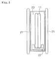
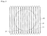
- An RTP furnace 25 of single wafer processing type is employed as the device for providing the heat treatment for cleavage, as shown in Figs. 1 to 3.
- This RTP furnace 25 can provide the control of the rate of temperature increase by as short as a unit of second in contrast with the batch type of furnace, so that it can heat the surface of the bonded wafer uniformly and rapidly.
- a reaction chamber 20 is arranged in the RTP furnace 25.
- the reaction chamber 20 is provided with a supporting jig 22 made of silica for holding the bonded wafer 11 vertical.
- a plurality of infrared lamps 21 serving as a heat source used for the heat treatment of the bonded wafer 11 is disposed laterally with respect to the top and the back surfaces of the bonded wafer 11 held vertically.
- the infrared lamp has an elongated configuration, and a plurality of those lamps is disposed vertically in the lateral sides with respect to the top and the back surfaces of the bonded wafer 11. This arrangement allows for the heat treatment for cleavage to be applied across the entire surface of the bonded wafer 11.
- a gas inlet port 26 is provided for introducing a gas into the reaction chamber 20.
- the bonded wafer 11 comprising the active layer wafer with the ion-implanted layer formed therein is held horizontal in a wafer charier 23, as shown in Fig. 3.
- the bonded wafer 11 is taken out of the wafer carrier 23 by using a wafer transport robot 24. Further, the bonded wafer 11 taken out of the carrier 23 is held vertical and transported into the reaction chamber 20 of the RTP furnace 25.
- the bonded wafer 11 after having been transported into the reaction chamber 20 is supported vertical by the supporting jig 22 made of silica in the reaction chamber 20.
- the temperature during the introduction of the bonded wafer 11 into the reaction chamber 20 is a room temperature. Then, the temperature within the reaction chamber 20 is increased from the room temperature to a set temperature defined by a range of 400°C to 1000°C (e.g. , 500°C) at a rate of temperature increase of 20°C /min, and the wafer 11 is held therein for 10 minutes. It is to be noted that if the rate of temperature increase exceeds 20°C/min, the temperature distribution across the wafer surface and thus a film thickness distribution across the SOI layer (i.e., the active layer) could be deteriorated. Therefore, preferably the rate of temperature increase should be 20°C/min or lower (see the result of below Table 3).
- the reaction chamber 20 is full of N 2 gas atmosphere as the N 2 gas has been introduced through a gas inlet port 26 into the reaction chamber 20.
- the bubbles of hydrogen ion that has been implanted into the active layer wafer of the bonded wafer 11 are formed.
- a part of the active layer wafer (a part of the bonded wafer 11) is cleaved and separated over its entire surface.
- the wafer 11 held vertical is heated uniformly and rapidly over its entire surface by the infrared lamps 21 disposed laterally with respect to the top and the back surfaces of the bonded wafer 11. This makes the temperature within the surface of the bonded wafer substantially uniform.
- a haze level in the cleaved surface (defined in the active layer wafer side) of the bonded wafer 11 was measured by using a surface detector (SFS6220). This was performed because the haze level tends to change in dependence on the thickness of the SOI layer and BOX layer (i.e. , the buried oxide film) in the SOI wafer.
- the bonded wafer 11 after the cleavage is processed based on a typical method for producing an SOI wafer in accordance with the smart cut method so as to be finally produced as an SOI wafer.
- the heat treatment is applied to the bonded wafer 11 in order to firmly bond the portion for the active layer wafer with the portion for the supporting wafer.
- the condition for this heat treatment it should be performed at the temperature of 1100°C or higher in the oxidizing gas atmosphere for approximately two hours.
- the SOI layer surface is ground, and then thus ground surface is further mirror polished so as to reduce the film thickness of the SOI layer for finishing the SOI wafer.
Landscapes
- Element Separation (AREA)
Abstract
Description
- The present invention relates to a method for producing an SOI wafer, and more particularly to a method for producing an SOI wafer in combination with a cleavage method comprising a hydrogen ion-implantation.
- An SOI wafer has been used in an LSI of high-speed low-power consumption, as it is considered superior to a conventional silicon wafer in some properties, including separation between devices, reduced parasitic capacity between a device and a substrate and a three-dimensional structure to be feasible.
One of methods for producing the SOI wafer in the prior art includes the smart cut method in which hydrogen ion is implanted into a silicon wafer surface and then the silicon wafer is bonded to another wafer, and subsequently thus obtained bonded wafer is subjected to a heat treatment for cleavage so as for a part of the silicon wafer to be cleaved and separated away at the site of ion-implanted layer serving as an interface layer. In this smart cut method, the wafer for an active layer that has been implanted with the hydrogen ion from the silicon wafer surface is bonded with the supporting wafer. Consequently, a bonded wafer having an insulating layer in the site of bonding interface is formed. After this step of process, thus bonded wafer is subjected to a heat treatment for cleavage. As for a set temperature used in the heat treatment for cleavage, as disclosed in Patent Document 1, for example, the heat treatment has to be carried out at approximately 500°C or higher. - Japanese Patent No. 3048201
- However, in this method, if a temperature distribution in a furnace, especially the temperature distribution within the surface of the bonded wafer, during the heat treatment for cleavage turns to be uneven, a re-arrangement of crystal and a void concentration within the surface are apt to be discontinuous. Further disadvantageously, there is a fear that it tends to deteriorate the uniformity of film thickness of an SOI layer, which would affect to subsequent steps for reducing the film thickness. There would be another problem that the above method produces a region in which the cleavage would not occur at the site of ion-implanted layer as the interface, inhibiting the SOI wafer from being produced.
- An object of the present invention is to provide a method for producing an SOI wafer according to the smart cut method, in which the temperature within the surface of the bonded wafer is made substantially uniform during the heat treatment for cleavage.
Another object of the present invention is to provide a method for producing an SOI wafer allowing for a complete cleavage through the entire wafer at the site of the ion-implanted layer serving as the interface without leaving any uncleaved region. - A first invention provides a method for producing an SOI wafer, comprising the steps of:
- ion-implanting of a noble gas element to a wafer for active layer via an insulating film to form an ion-implanted layer in the active layer wafer;
- subsequently bonding the active layer wafer with a supporting wafer via the insulating film disposed therebetween to form a bonded wafer; and then
- heat treating the bonded wafer while holding it at a set temperature so as to cleave and separate a part of the active layer wafer at a site of ion-implanted layer as an interface, wherein
- in the heat treatment, a temperature variation within a surface of the bonded wafer is controlled to be 40°C or smaller so as to achieve the cleavage at the site of said ion-implanted layer as the interface.
- In the method for producing the SOI wafer according to the first invention, firstly the ion-implanted layer is formed in the active layer wafer (e.g. , a wafer comprising an oxide film formed on top of a silicon wafer). Subsequently, this active layer wafer is bonded with the supporting wafer (e.g., a silicon wafer) via the insulating film interposed therebetween. This bonding process of the active layer wafer with the supporting wafer consequently produces a bonded wafer with the intervention of the insulating film at the site of bonding surface. After this step of processing, the bonded wafer is heat treated at the set temperature (e.g. , temperature in a range of 400°C to 1000°C). During this process, the temperature variation within the surface of the bonded wafer has been controlled within 40°C. Accordingly, bubbles of noble gas are formed in the ion-implanted layer, and the cleavage occurs at the site of ion-implanted layer as the interface. In this case, since the temperature within the surface of the bonded wafer has been held substantially uniform, it hardly produces any regions that will be left without occurrence of cleavage but a complete cleavage would be induced over the entire surface of the bonded wafer at the site of ion-implanted layer as the interface.
- Thus, according to the first invention, in the method for producing the SOI wafer in accordance with the smart cut method, the temperature variation within the surface of the bonded wafer during the heat treatment for cleavage is controlled within 40°C. For example, assuming that the temperature at which the cleavage starts is 410°C or higher, the cleavage takes effect in a region in the surface of the bonded wafer where the temperature is in a range of 410°C to 450°C. However, the wafer is forced to be cleaved and separated at the site of bonding interface specifically in a region at the temperature of 400°C. Consequently, the SOI wafer partially lacking the SOI structure would be produced. It implies that the temperature variation within the surface of the bonded wafer immediately after the starting of the cleavage should be controlled to be within 40°C.
A diameter of the bonded wafer to be treated may be, for example, 200mm or 300mm.
Preferably, a heat treatment device used to provide the heat treatment for cleavage is an RTP (Rapid Thermal Processing) furnace of single wafer processing type. This is because the bonded wafer can be heated rapidly and uniformly by applying lamp heating to the wafers one by one in the single wafer processing type of furnace. On the other hand, it is difficult to control the temperature variation within the surface of the bonded wafer to be within 40°C in a furnace of batch type where the heating rate of the bonded wafer varies depending on the introduction temperature and the introduction rate. If the batch type of furnace is used, the rate of temperature increase to the cleavage starting temperature should be controlled to be 20°C/min, for example, for carrying out the heat treatment for cleavage. With the rate of temperature increase over 20°C/min, there will be a local region within the wafer surface that is not able to follow the temperature increase. This may cause uneven temperature distribution across the wafer surface. Accordingly, if the rate of temperature increase is set to be 20°C /min or lower, the temperature variation over the entire surface of the bonded wafer can be controlled within 40°C easily and accurately. - A second invention provides a method for producing an SOI wafer as defined in the first invention, in which the set temperature is in a range of 400°C to 1000°C.
- In the method for producing the SOI wafer according to the second embodiment, the set temperature for the heat treatment for cleavage of the bonded wafer has employed a range of 400°C to 1000°C . The set temperature below 400°C may be associated with a problem that the cleavage starting temperature of the bonded wafer would not be reached, failing in inducing the cleavage. With the temperature over 1000°C, such a problem may occur that a reaction tube (silica tube) of the heat treatment device could be deformed. There will be another problem arisen that the portions of the bonded wafer, which have been once separated, are brought into contact with each other at the site of interface and thus form a bond therein, where it will be difficult to make a cleavage later again. Specifically, it is required that the entire surface of the bonded wafer should be in a temperature range of 400°C to 1000°C and that the temperature variation within the surface should be 40°C in maximum.
For the case employing the batch type of furnace, the temperature within the furnace during the introduction is required to be suppressed to 400°C or lower, and if taking the throughput in production of the SOI wafer into account, preferably the temperature within the furnace during the introduction is in a range of 300°C to 400°C. That is, the bonded wafer can be heated while keeping the small temperature variation within the surface of the bonded wafer by setting the introduction temperature at 400°C or lower. - A third invention provides a method for producing an SOI wafer as defined in the second invention, in which the heat treatment is performed while holding the bonded wafer substantially vertical so as to induce the cleavage in the bonded wafer at the site of ion-implanted layer as the interface.
A heat source for heating the bonded wafer while holding the bonded wafer substantially vertical is disposed in proximal to the top and the back surfaces of the bonded wafer. The heat source may employ an infrared lamp, for example. - In the method for producing the SOI wafer according to the third invention, the bonded wafer is held vertical by a supporting jig made of silica disposed in a reaction chamber within the RTP furnace. Then, this bonded wafer is heat treated by the infrared lamp disposed laterally with respect to the top and the back surfaces of the bonded wafer.
The reason why the bonded wafer is held vertical is to prevent the cleaved and separated wafers after the heat treatment for cleavage from coming into contact with each other again. Then, the entire surface of this bonded wafer is heated uniformly and rapidly to thereby make the temperature within the surface of the bonded wafer substantially uniform. Thus, the complete cleavage can be achieved across the entire surface of the bonded wafer at the site of the ion-implanted layer as the interface. - According to the present invention, in the method for producing the SOI wafer in accordance with the smart cut method, a bonded wafer is heat treated at a set temperature in a range of 400°C to 1000°C. In this process, a temperature variation within the surface of the bonded wafer is controlled to be within 40°C. Consequently, bubbles of noble gas are formed in an ion-implanted layer, and the bonded wafer is cleaved and separated (i.e., a part of the active layer wafer is separated from the remaining part of the SOI wafer) at the site of the ion-implanted layer specifically in a region containing thus formed bubbles as the interface. Under this condition, the temperature within the surface of the bonded wafer has been substantially uniform. Owing to this, the complete cleavage can be achieved across the entire surface of the wafer at the site of the ion-implanted layer as the interface without producing any region that have been left not-cleaved.
-
- Fig. 1 is a front view showing a configuration of a device for providing a heat treatment for cleavage of a bonded wafer according to one embodiment of the present invention;
- Fig. 2 is a side view showing a configuration of a device for providing a heat treatment for cleavage of a bonded wafer according to one embodiment of the present invention; and
- Fig. 3 is a side view showing a configuration of a transport device for transporting a bonded wafer to a device for providing a heat treatment for cleavage according to one embodiment of the present invention. Description of reference numerals
- 11 SOI wafer
- A preferred embodiment of the present invention will now be described with reference to the attached drawings.
- One embodiment of the present invention will now be described with reference to Figs. 1 to 3.
A method for producing anSOI wafer 11 in accordance with the smart cut method according to the present invention is carried out in the following manner.
Firstly, two pieces of silicon wafer are prepared, which have been made by slicing an ingot of monocrystal silicon grown in the CZ method and doped with boron. One of those prepared silicon wafers serves as an active layer wafer and the other of those silicon wafers serves as a supporting wafer. Then, an oxide film is formed on top of the silicon wafer prepared to be the active layer wafer. The formation of the silicon oxide film is achieved by introducing the silicon wafer into an oxidizing furnace and heating the silicon wafer at a predetermined temperature for a predetermined time. The silicon oxide film to be formed in this process may have a thickness of 150nm. - Secondly, the silicon wafer with the oxide film formed thereon is set in a vacuum chamber of an ion-implanting device. Then, a predetermined dose of hydrogen ion is implanted into the active layer wafer from its surface through the oxide film. Consequently an ion-implanted layer is formed in the active layer wafer at the predetermined depth (extending across a predetermined range of depth within the silicon wafer).
Subsequently, the active layer wafer with the hydrogen ion implanted therein is bonded with the supporting wafer at the side of ion-implanted surface (i.e., oxide film surface) used as the bonding surface for the active layer wafer. Resultantly, a bonded wafer including an insulating film (i.e., the oxide film) intervening in the bonding surface is formed.
Those steps to be taken up to this stage of processing are analogous to the steps employed in a method for producing the SOI wafer in a typical smart cut method. - A device used for the heat treatment for cleavage of the bonded
wafer 11 will now be described.
AnRTP furnace 25 of single wafer processing type is employed as the device for providing the heat treatment for cleavage, as shown in Figs. 1 to 3. ThisRTP furnace 25 can provide the control of the rate of temperature increase by as short as a unit of second in contrast with the batch type of furnace, so that it can heat the surface of the bonded wafer uniformly and rapidly.
Areaction chamber 20 is arranged in theRTP furnace 25. Thereaction chamber 20 is provided with a supportingjig 22 made of silica for holding the bondedwafer 11 vertical. Further, a plurality ofinfrared lamps 21 serving as a heat source used for the heat treatment of the bondedwafer 11 is disposed laterally with respect to the top and the back surfaces of the bondedwafer 11 held vertically. The infrared lamp has an elongated configuration, and a plurality of those lamps is disposed vertically in the lateral sides with respect to the top and the back surfaces of the bondedwafer 11. This arrangement allows for the heat treatment for cleavage to be applied across the entire surface of the bondedwafer 11. Further, as shown in Fig. 3, agas inlet port 26 is provided for introducing a gas into thereaction chamber 20. - Subsequently, a method of heat treatment for cleavage of the bonded
wafer 11 will now be described.
The bondedwafer 11 comprising the active layer wafer with the ion-implanted layer formed therein is held horizontal in awafer charier 23, as shown in Fig. 3. The bondedwafer 11 is taken out of thewafer carrier 23 by using awafer transport robot 24. Further, the bondedwafer 11 taken out of thecarrier 23 is held vertical and transported into thereaction chamber 20 of theRTP furnace 25. The bondedwafer 11 after having been transported into thereaction chamber 20 is supported vertical by the supportingjig 22 made of silica in thereaction chamber 20. In this step of process, the temperature during the introduction of the bondedwafer 11 into thereaction chamber 20 is a room temperature.
Then, the temperature within thereaction chamber 20 is increased from the room temperature to a set temperature defined by a range of 400°C to 1000°C (e.g. , 500°C) at a rate of temperature increase of 20°C /min, and thewafer 11 is held therein for 10 minutes. It is to be noted that if the rate of temperature increase exceeds 20°C/min, the temperature distribution across the wafer surface and thus a film thickness distribution across the SOI layer (i.e., the active layer) could be deteriorated. Therefore, preferably the rate of temperature increase should be 20°C/min or lower (see the result of below Table 3).
Thereaction chamber 20 is full of N2 gas atmosphere as the N2 gas has been introduced through agas inlet port 26 into thereaction chamber 20. Under this condition, the bubbles of hydrogen ion that has been implanted into the active layer wafer of the bondedwafer 11 are formed. Then, at the site of the ion-implanted layer containing thus formed bubbles as the interface, a part of the active layer wafer (a part of the bonded wafer 11) is cleaved and separated over its entire surface.
In this stage of process, thewafer 11 held vertical is heated uniformly and rapidly over its entire surface by theinfrared lamps 21 disposed laterally with respect to the top and the back surfaces of the bondedwafer 11. This makes the temperature within the surface of the bonded wafer substantially uniform. This induces a complete cleavage and separation of the wafer at the site of the ion-implanted layer as the interface. Further, the bondedwafer 11 is heat treated for cleavage as it is held to be vertical. Therefore, this can prevent the portions of wafers after their having been cleaved and separated from being brought into contact with each other later again.
After the heat treatment for cleavage, a haze level in the cleaved surface (defined in the active layer wafer side) of the bondedwafer 11 was measured by using a surface detector (SFS6220). This was performed because the haze level tends to change in dependence on the thickness of the SOI layer and BOX layer (i.e. , the buried oxide film) in the SOI wafer. The result from the measurement showed that the haze level equal to or higher than 2000ppm was not confirmed in the cleaved surface of the bondedwafer 11, thus demonstrating that the cleavage process had been successfully performed to form the uniform cleavage over the entire surface. - The bonded
wafer 11 after the cleavage is processed based on a typical method for producing an SOI wafer in accordance with the smart cut method so as to be finally produced as an SOI wafer. Specifically, the heat treatment is applied to the bondedwafer 11 in order to firmly bond the portion for the active layer wafer with the portion for the supporting wafer. As for the condition for this heat treatment, it should be performed at the temperature of 1100°C or higher in the oxidizing gas atmosphere for approximately two hours.
Finally, the SOI layer surface is ground, and then thus ground surface is further mirror polished so as to reduce the film thickness of the SOI layer for finishing the SOI wafer. - Subsequently, for the heat treatment for cleavage of the bonded
wafer 11, an experiment was conducted under different conditions as defined below. Specifically, - (1) an experiment in order to determine the SOI layer distribution and the presence of any regions where the cleavage has not occurred by varying the temperature difference within the surface of the bonded
wafer 11 during the heat treatment for cleavage (Table 1); - (2) an experiment in order to determine the SOI layer distribution and the presence of any regions where the cleavage has not occurred on the bonded
wafer 11 that was introduced into a batch type of furnace under the condition of temperature in a range of 300°C to 700°C, and after the temperature having increased to 700°C, held for 30 minutes, and then taken out of the furnace (Table 2); and - (3) an experiment in order to determine the SOI layer distribution and the presence of any regions where the cleavage has not occurred on the bonded
wafer 11 that was introduced into a batch type of furnace under the condition of temperature at 300°C, and subjected to the heat treatment for cleavage with different rates of temperature increase up to 500°C, and then taken out of the furnace (Table 3), were conducted, respectively. - It has been confirmed from the above experiment results that if the temperature difference within the surface of the bonded
wafer 11 is controlled to be within 40°C, then the bondedwafer 11 can be cleaved and separated completely across the entire surface. It has been further confirmed that if the heat treatment for cleavage is carried out with the set temperature in a range of 400°C to 1000°C, when employing the batch type of furnace, then thebondedwafer 11 can be cleaved and separated completely across the entire surface without leaving any uncleaved regions. It has been also confirmed that if the heat treatment for cleavage is carried out with the rate of temperature increase set to 20°C /min or lower, when employing the batch type of furnace, then the bondedwafer 11 can be cleaved and separated completely across the entire surface without leaving any uncleaved regions.
| In-surface temperature difference | 35°C | 40°c | 45°C | 50°c | 60°C |
| SOI layer distribution | NIL | NIL | Present | Present | Present |
| Region of no cleavage occurred | NIL | NIL | NIL | NIL | Present |
| Introduction temperature | 300°C | 400°C | 500°C | 600°C | 700°C |
| SOI layer distribution | NIL | NIL | Present | Present | Present |
| Region of no cleavage occurred | NIL | NIL | NIL | NIL | Present |
| Rate of temperature increase | 5°C /min | 10°C /min | 200°C/ | 25°C/min | 30°C/min |
| SOI layer distribution | NIL | NIL | NIL | Present | Present |
| Region of no cleavage occurred | NIL | NIL | NIL | NIL | Present |
Claims (3)
- A method for producing an SOI wafer, comprising the steps of ion-implanting of a noble gas element to a wafer for active layer via an insulating film to form an ion-implanted layer in said active layer wafer;
subsequently bonding said active layer wafer with a supporting wafer via the insulating film disposed therebetween to form a bonded wafer; and then
heat treating saidbondedwaferwhileholding it at a set temperature so as to cleave and separate a part of said active layer wafer at the site of ion-implanted layer as an interface, wherein
in said heat treatment, a temperature variation within a surface of said bonded wafer is controlled to be 40°C or smaller so as to achieve the cleavage at the site of said ion-implanted layer as the interface. - A method for producing an SOI wafer in accordance with claim 1, in which said set temperature is in a range of 400°C to 1000°C.
- A method for producing an SOI wafer in accordance with claim 1 or 2, in which said heat treatment is performed while holding said bonded wafer substantially vertical so as to induce the cleavage in said bonded wafer at the site of ion-implanted layer as the interface.
Applications Claiming Priority (2)
| Application Number | Priority Date | Filing Date | Title |
|---|---|---|---|
| JP2003314758 | 2003-09-05 | ||
| PCT/JP2004/012728 WO2005024916A1 (en) | 2003-09-05 | 2004-09-02 | Method for producing soi wafer |
Publications (3)
| Publication Number | Publication Date |
|---|---|
| EP1662550A1 true EP1662550A1 (en) | 2006-05-31 |
| EP1662550A4 EP1662550A4 (en) | 2007-07-04 |
| EP1662550B1 EP1662550B1 (en) | 2019-12-04 |
Family
ID=34269816
Family Applications (1)
| Application Number | Title | Priority Date | Filing Date |
|---|---|---|---|
| EP04772682.3A Expired - Lifetime EP1662550B1 (en) | 2003-09-05 | 2004-09-02 | Method for producing soi wafer |
Country Status (4)
| Country | Link |
|---|---|
| US (1) | US7510948B2 (en) |
| EP (1) | EP1662550B1 (en) |
| JP (1) | JPWO2005024916A1 (en) |
| WO (1) | WO2005024916A1 (en) |
Cited By (1)
| Publication number | Priority date | Publication date | Assignee | Title |
|---|---|---|---|---|
| EP2023380A1 (en) * | 2007-08-08 | 2009-02-11 | S.O.I.T.E.C. Silicon on Insulator Technologies | Method and installation for fracturing a composite substrate via an embrittlement plane |
Families Citing this family (6)
| Publication number | Priority date | Publication date | Assignee | Title |
|---|---|---|---|---|
| JP5082299B2 (en) * | 2006-05-25 | 2012-11-28 | 株式会社Sumco | Manufacturing method of semiconductor substrate |
| JP2008066500A (en) * | 2006-09-07 | 2008-03-21 | Sumco Corp | Bonded wafer and manufacturing method thereof |
| JP5493343B2 (en) | 2008-12-04 | 2014-05-14 | 信越半導体株式会社 | Manufacturing method of bonded wafer |
| JP2011082443A (en) * | 2009-10-09 | 2011-04-21 | Sumco Corp | Epitaxial wafer and method for manufacturing the same |
| US8845859B2 (en) | 2011-03-15 | 2014-09-30 | Sunedison Semiconductor Limited (Uen201334164H) | Systems and methods for cleaving a bonded wafer pair |
| CN104025277A (en) | 2011-10-31 | 2014-09-03 | Memc电子材料有限公司 | Clamping device and cleaving method for cleaving bonded wafer structures |
Family Cites Families (11)
| Publication number | Priority date | Publication date | Assignee | Title |
|---|---|---|---|---|
| US134489A (en) * | 1872-12-31 | Improvement in nut-fastenimgs | ||
| US216008A (en) * | 1879-05-27 | Improvement in line-holders | ||
| US5059770A (en) * | 1989-09-19 | 1991-10-22 | Watkins-Johnson Company | Multi-zone planar heater assembly and method of operation |
| FR2681472B1 (en) * | 1991-09-18 | 1993-10-29 | Commissariat Energie Atomique | PROCESS FOR PRODUCING THIN FILMS OF SEMICONDUCTOR MATERIAL. |
| JPH11307747A (en) * | 1998-04-17 | 1999-11-05 | Nec Corp | SOI substrate and manufacturing method thereof |
| FR2834820B1 (en) * | 2002-01-16 | 2005-03-18 | METHOD FOR CLEAVING LAYERS OF A MATERIAL WAFER | |
| FR2839385B1 (en) * | 2002-05-02 | 2004-07-23 | Soitec Silicon On Insulator | PROCESS FOR TAKING OFF MATERIAL LAYERS |
| KR100511656B1 (en) * | 2002-08-10 | 2005-09-07 | 주식회사 실트론 | Method of fabricating nano SOI wafer and nano SOI wafer fabricated by the same |
| US7052978B2 (en) * | 2003-08-28 | 2006-05-30 | Intel Corporation | Arrangements incorporating laser-induced cleaving |
| WO2005024918A1 (en) * | 2003-09-08 | 2005-03-17 | Sumco Corporation | Soi wafer and its manufacturing method |
| JPWO2005027217A1 (en) * | 2003-09-08 | 2007-11-08 | 株式会社Sumco | SOI wafer and manufacturing method thereof |
-
2004
- 2004-09-02 WO PCT/JP2004/012728 patent/WO2005024916A1/en not_active Ceased
- 2004-09-02 EP EP04772682.3A patent/EP1662550B1/en not_active Expired - Lifetime
- 2004-09-02 JP JP2005513661A patent/JPWO2005024916A1/en active Pending
- 2004-09-02 US US10/570,354 patent/US7510948B2/en not_active Expired - Fee Related
Cited By (3)
| Publication number | Priority date | Publication date | Assignee | Title |
|---|---|---|---|---|
| EP2023380A1 (en) * | 2007-08-08 | 2009-02-11 | S.O.I.T.E.C. Silicon on Insulator Technologies | Method and installation for fracturing a composite substrate via an embrittlement plane |
| FR2919960A1 (en) * | 2007-08-08 | 2009-02-13 | Soitec Silicon On Insulator | METHOD AND INSTALLATION FOR FRACTURE OF A COMPOSITE SUBSTRATE ACCORDING TO A FRAGILIZATION PLAN |
| US8324078B2 (en) | 2007-08-08 | 2012-12-04 | Soitec | Method and installation for fracturing a composite substrate along an embrittlement plane |
Also Published As
| Publication number | Publication date |
|---|---|
| US7510948B2 (en) | 2009-03-31 |
| EP1662550A4 (en) | 2007-07-04 |
| JPWO2005024916A1 (en) | 2007-11-08 |
| EP1662550B1 (en) | 2019-12-04 |
| US20060266437A1 (en) | 2006-11-30 |
| WO2005024916A1 (en) | 2005-03-17 |
Similar Documents
| Publication | Publication Date | Title |
|---|---|---|
| KR100750978B1 (en) | Semiconductor wafer with layer structure with low warp and bow, and process for producing it | |
| US7867877B2 (en) | Method for manufacturing SOI wafer | |
| US7579654B2 (en) | Semiconductor on insulator structure made using radiation annealing | |
| EP1662549B1 (en) | Method for manufacturing bonded wafer | |
| EP2343729B1 (en) | Method for manufacturing silicon thin film transfer insulating wafer | |
| US7323398B2 (en) | Method of layer transfer comprising sequential implantations of atomic species | |
| EP2259299A1 (en) | Method for manufacturing SOI wafer, and SOI wafer | |
| EP1662555B1 (en) | Method for producing soi wafer | |
| EP2686878A1 (en) | Silicon on insulator structures having high resistivity regions in the handle wafer and methods for producing such structures | |
| EP2802001A1 (en) | Method for manufacturing bonded silicon-on-insulator (soi) wafer | |
| KR20060126629A (en) | Surface finish method of SOI substrate using epitaxial process | |
| US20010016402A1 (en) | Smoothing method for cleaved films made using thermal treatment | |
| EP1662550B1 (en) | Method for producing soi wafer | |
| US7858494B2 (en) | Laminated substrate manufacturing method and laminated substrate manufactured by the method | |
| JP2019004173A (en) | Production of high precipitate density wafers by activation of inactive oxygen precipitate nuclei by heat treatment | |
| EP1791175A2 (en) | Method of manufacturing bonded wafer | |
| CN108701593A (en) | Heat treatment method for semiconductor wafer | |
| KR102914139B1 (en) | Method of transferring semiconductor layers | |
| EP1298731B1 (en) | Simox substrate production process | |
| US7494899B2 (en) | Method for manufacturing semiconductor substrate | |
| EP1697981B1 (en) | Process for improving the surface roughness of a semiconductor wafer | |
| US20250391704A1 (en) | Method for transferring a thin layer onto a support substrate | |
| CN120642026A (en) | Method for forming a weakened area in a semiconductor substrate | |
| JPH1092759A (en) | Substrate heat treatment apparatus and substrate heat treatment method |
Legal Events
| Date | Code | Title | Description |
|---|---|---|---|
| PUAI | Public reference made under article 153(3) epc to a published international application that has entered the european phase |
Free format text: ORIGINAL CODE: 0009012 |
|
| 17P | Request for examination filed |
Effective date: 20060302 |
|
| AK | Designated contracting states |
Kind code of ref document: A1 Designated state(s): FR |
|
| DAX | Request for extension of the european patent (deleted) | ||
| RBV | Designated contracting states (corrected) |
Designated state(s): FR |
|
| A4 | Supplementary search report drawn up and despatched |
Effective date: 20070605 |
|
| RIC1 | Information provided on ipc code assigned before grant |
Ipc: H01L 27/12 20060101ALI20070530BHEP Ipc: H01L 21/265 20060101ALI20070530BHEP Ipc: H01L 21/02 20060101ALI20070530BHEP Ipc: H01L 21/762 20060101AFI20070530BHEP |
|
| 17Q | First examination report despatched |
Effective date: 20070813 |
|
| GRAP | Despatch of communication of intention to grant a patent |
Free format text: ORIGINAL CODE: EPIDOSNIGR1 |
|
| INTG | Intention to grant announced |
Effective date: 20190606 |
|
| GRAS | Grant fee paid |
Free format text: ORIGINAL CODE: EPIDOSNIGR3 |
|
| GRAJ | Information related to disapproval of communication of intention to grant by the applicant or resumption of examination proceedings by the epo deleted |
Free format text: ORIGINAL CODE: EPIDOSDIGR1 |
|
| GRAL | Information related to payment of fee for publishing/printing deleted |
Free format text: ORIGINAL CODE: EPIDOSDIGR3 |
|
| GRAR | Information related to intention to grant a patent recorded |
Free format text: ORIGINAL CODE: EPIDOSNIGR71 |
|
| GRAA | (expected) grant |
Free format text: ORIGINAL CODE: 0009210 |
|
| INTC | Intention to grant announced (deleted) | ||
| AK | Designated contracting states |
Kind code of ref document: B1 Designated state(s): FR |
|
| INTG | Intention to grant announced |
Effective date: 20191029 |
|
| PLBE | No opposition filed within time limit |
Free format text: ORIGINAL CODE: 0009261 |
|
| STAA | Information on the status of an ep patent application or granted ep patent |
Free format text: STATUS: NO OPPOSITION FILED WITHIN TIME LIMIT |
|
| 26N | No opposition filed |
Effective date: 20200907 |
|
| PG25 | Lapsed in a contracting state [announced via postgrant information from national office to epo] |
Ref country code: FR Free format text: LAPSE BECAUSE OF NON-PAYMENT OF DUE FEES Effective date: 20200930 |