EP1659690A1 - Comparator for input voltages higher than supply voltage - Google Patents
Comparator for input voltages higher than supply voltage Download PDFInfo
- Publication number
- EP1659690A1 EP1659690A1 EP04078179A EP04078179A EP1659690A1 EP 1659690 A1 EP1659690 A1 EP 1659690A1 EP 04078179 A EP04078179 A EP 04078179A EP 04078179 A EP04078179 A EP 04078179A EP 1659690 A1 EP1659690 A1 EP 1659690A1
- Authority
- EP
- European Patent Office
- Prior art keywords
- transistor
- comparator
- voltage
- input
- coupled
- Prior art date
- Legal status (The legal status is an assumption and is not a legal conclusion. Google has not performed a legal analysis and makes no representation as to the accuracy of the status listed.)
- Granted
Links
- 230000003071 parasitic effect Effects 0.000 claims description 3
- XUIMIQQOPSSXEZ-UHFFFAOYSA-N Silicon Chemical compound [Si] XUIMIQQOPSSXEZ-UHFFFAOYSA-N 0.000 abstract description 11
- 229910052710 silicon Inorganic materials 0.000 abstract description 11
- 239000010703 silicon Substances 0.000 abstract description 11
- 238000005516 engineering process Methods 0.000 description 11
- 238000000034 method Methods 0.000 description 4
- 230000010354 integration Effects 0.000 description 3
- 239000004065 semiconductor Substances 0.000 description 3
- 238000007796 conventional method Methods 0.000 description 2
- 238000001514 detection method Methods 0.000 description 2
- 238000012544 monitoring process Methods 0.000 description 2
- 230000000694 effects Effects 0.000 description 1
- 238000012986 modification Methods 0.000 description 1
- 230000004048 modification Effects 0.000 description 1
- 229920006395 saturated elastomer Polymers 0.000 description 1
- 230000035945 sensitivity Effects 0.000 description 1
- 230000011664 signaling Effects 0.000 description 1
- 230000007704 transition Effects 0.000 description 1
Images




Classifications
-
- H—ELECTRICITY
- H03—ELECTRONIC CIRCUITRY
- H03K—PULSE TECHNIQUE
- H03K5/00—Manipulating of pulses not covered by one of the other main groups of this subclass
- H03K5/01—Shaping pulses
- H03K5/08—Shaping pulses by limiting; by thresholding; by slicing, i.e. combined limiting and thresholding
-
- H—ELECTRICITY
- H03—ELECTRONIC CIRCUITRY
- H03K—PULSE TECHNIQUE
- H03K5/00—Manipulating of pulses not covered by one of the other main groups of this subclass
- H03K5/22—Circuits having more than one input and one output for comparing pulses or pulse trains with each other according to input signal characteristics, e.g. slope, integral
- H03K5/24—Circuits having more than one input and one output for comparing pulses or pulse trains with each other according to input signal characteristics, e.g. slope, integral the characteristic being amplitude
- H03K5/2472—Circuits having more than one input and one output for comparing pulses or pulse trains with each other according to input signal characteristics, e.g. slope, integral the characteristic being amplitude using field effect transistors
Definitions
- This invention relates to comparators, and to integrated circuits having such comparators, and to devices having such integrated circuits as well as to methods of operating and making these.
- US patent 5,942,921 is concerned with this issue and shows a solution for interfacing low voltage circuitry to high voltage circuitry, and in particular, to an interface circuit which operates from the low voltage power supply to detect differential signals which may have signal voltages that exceed the voltage of the low power supply.
- a first transistor and a first resistor coupled in series are coupled in parallel with a second transistor and a second series resistor.
- the transistor drain terminals are both coupled to the power supply voltage, and a current source draws current from the common node of the resistors.
- Input voltages are supplied to the gates of the transistors, and the differential output voltages are provided from the transistor source terminals.
- a differential amplifier receives the differential output voltages and provides a single output voltage.
- the differential buffer transistors are exposed to only the differences between the input voltages and the power supply voltage, and consequently may not be subject to failure if the input voltage exceeds the power supply voltage. Further, the current carrying capacity of the transistors is modulated by the input voltages regardless of whether the input voltages exceed the supply voltages or not, thereby allowing differential detection even with signal voltages that exceed the power supply voltage.
- the value of the resistance should be high. This is useful for thermal management of products as well as battery life of mobile products. However this often conflicts or is incompatible with using only a small area of silicon to reduce costs and increase integration levels.
- An object of the invention is to provide improved apparatus or methods, especially comparators, and integrated circuits having such comparators, and devices having such integrated circuits as well as methods of operating and making these.
- the invention provides a comparator for comparing voltages of first and second inputs, and having first and second current paths coupled to the first and second inputs respectively, the first current path passing from the first input through a first main electrode such as a drain and second main electrode, e.g. a source of a first transistor, and through a first bias current source to a supply line, the second current path passing through a reference voltage drop element, through a first main electrode, e.g. a drain and a second main electrode, e.g. a source of a second transistor, and through a second bias current source to a supply line.
- the comparator may be implemented in CMOS or BiCMOS technology, for example and less preferred in bipolar technology.
- the first and second transistors (M1 and M2) are preferably MOS transistors.
- the comparator is implemented with a current mirror arrangement, but the additional reference voltage drop element enables higher voltages to be input and compared to an internal supply voltage level without the need for resistive dividers.
- the higher thresholds could be achieved by combining the conventional technique of a differential amplifier arrangement with the conventional voltage dropping resistive dividers on one or both inputs, but at a cost of higher power dissipation, i.e. due to the limitation imposed on the size of integrated resistors.
- the advantages are based on a recognition that the power dissipation of the comparator is determined by the biasing current sources only, and the area of semiconductor, e.g. silicon used by current sources is usually smaller than the area used by resistors of sufficient resistance to limit the current at the level imposed by these current sources.
- An additional advantage is that the inputs of the comparator are not connected to control electrodes of transistors, e.g. gates of MOS transistors, which should improve the resistance of the component to ESD.
- transistors e.g. gates of MOS transistors
- the power dissipation and or the semiconductor, e.g. silicon area used can be kept lower than known arrangements using dividing resistors.
- the reference voltage drop element can include a resistance (less preferred), and or one or more diode drops or other circuitry.
- the reference voltage drop can be embodied by, for example, any one or any combination of the following:
- An additional feature of the present invention is the first and second transistors, e.g. transistors M1 and M2, being PMOS transistors.
- Another such feature is the control electrodes, e.g. gates of the first and second transistors being coupled together.
- Another such feature is the first main electrodes, e.g. drains of the first and second transistors being coupled to the first and second current sources respectively.
- the first input is fed to the second main electrode, e.g. source of the first transistor.
- the second input is applied to one of the electrodes of the voltage drop element.
- Another such feature is the control electrode, e.g. gate and the first main electrode, e.g. drain of the first transistor being coupled together.
- Another such feature is the voltage drop element comprising one or more transistors.
- Another such feature is an output being taken from a first main electrode, e.g. drain of the second transistor.
- Another such feature is a third transistor in the first current path and coupled to the first main electrode, e.g. drain of the first transistor.
- the third transistor is connected between the first transistor and the current source in the first current path to limit the voltage at the positive electrode of the current source.
- a fourth transistor can be included in the second current path and coupled to a first main electrode, e.g. drain of the second transistor and the current source in the second current path to limit overvoltage at the positive electrode of the current source.
- Another such feature is circuitry coupled between the second main electrode, e.g. source, and a control electrode, e.g. gate of the second transistor to limit overvoltage. This is useful for enabling implementation in technologies vulnerable to such overvoltage.
- Another such feature is a diode coupled to the first input to protect the first input from current flow through forward biasing of a parasitic diode from drain to bulk of the first transistor.
- Another aspect of the invention provides an integrated circuit having the comparator. Another aspect provides a battery powered mobile device having the integrated circuit. This is based on a recognition that the advantages of the integrated circuit can feed through to such devices to improve the device performance.
- transistors These are three-terminal devices: a first main electrode such as a drain, a second main electrode such as a source and a control electrode such as a gate for controlling the follow of electrical charges between the first and second main electrodes.
- Fig 1 shows a circuit known from US 5,942,921.
- This includes a differential buffer for a differential amplifier 202.
- the differential buffer includes a transistor 402 in series with a resistance 404, coupled in parallel with a second transistor 406 matched to the first (402) and a second resistance 408 equal to the first (404).
- the common node shared by transistors 402 and 406 is coupled to the supply voltage, and the common node shared by the resistances 404 and 408 is connected to ground via a current source 410.
- the input voltages are provided to the gates of the transistors 402 and 406, and the output voltages are provided to the differential amplifier inputs from the transistor source terminals.
- the differential buffer protects the differential amplifier from excess input signal voltages.
- the differential buffer transistors are can be driven by input voltage signals up to twice the power supply voltage, and the differential configuration of the buffer provides for continued differential signal detection at voltages above the power supply voltage.
- the current source 410 and the resistances 404 and 408 are chosen so that as long as the difference between the input signal voltages is greater than a few millivolts, the output voltage difference saturates at approximately the power supply voltage.
- the uniform voltage swing at the input to the differential amplifier then provides for a fixed propagation delay, thereby eliminating sensitivity of the output voltage to the size of input voltage swings.
- Fig 2 shows a circuit from FR 2 838 840.
- the comparator is provided to compare an input voltage V1 and an input voltage V2, and to deliver an output signal CS set to 1 when one of the voltages is higher than the other, or set to 0 in the opposite case.
- the comparator COMP comprises two PMOS transistors TP1, TP2 having their gates G interconnected.
- the source S of the transistor TP1 forms the first input of the comparator and receives the voltage V1.
- the source S of the transistor TP2 forms the second input of the comparator and receives the voltage V2.
- the bulk of the transistor TP1 is taken to the source potential of the transistor, and therefore receives the voltage V1.
- the bulk of the transistor TP2 is also taken to the source potential of the transistor, and therefore receives the voltage V2.
- the output of the comparator which delivers the signal CS, is connected to the drain of the transistor TP2.
- the transistors TP1, TP2 are in two branches arranged as current mirrors.
- the first branch comprises the transistor TP1 in series with a transistor TN1
- the second branch comprises the transistor TP2 in series with a transistor TN2.
- the transistor TP1 has its gate G connected to its drain D, which is connected to the drain D of the transistor TN1.
- the drain of the transistor TP2 is connected to the drain of the transistor TN2.
- the sources of the transistors TN1, TN2 are linked to ground, and the gates of the transistors TN1 and TN2 are biased by a voltage Vref(I).
- the voltage Vref(I) is delivered by a reference voltage generator, not represented here.
- the voltage Vref(I) is substantially equal to the threshold voltage of the transistors TN1, TN2 such that the latter operate in a saturated mode and are, as a result, equivalent to current sources.
- the comparator COMP operates as a differential amplifier comparing the source voltages of the transistors TP1 and TP2, i.e., the voltages V1 and V2.
- V2 the voltages of the transistors TP1 and TP2
- V1-e the voltages of the transistors TP1 and V2.
- Transistor TP2 is on and delivers a greater current than the transistor TP1. Since the drain currents of transistors TN1 and TN2 are assumed to be identical, the output signal CS rises and becomes equal to the voltage V2, i.e., the logic level 1. In summary, the transistor TP2 is blocked and the output CS is 0 when the voltage V2 is lower than V1. The transistor TP2 is on and the output CS is 1 when the voltage V2 is higher than V1. There is no suggestion here of how to enable the input voltages to be much greater than the supply voltage.
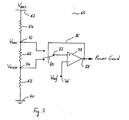
- Fig 3 shows another voltage monitor circuit 60 known from US patent 6,304,088. It can be used to monitor any voltage and provide an output signal indicative of the value or a status of the voltage being monitored.
- a resistor network of three resistors is employed to scale the battery voltage to provide the desired high and low monitor voltage levels.
- the resistance of each of resistors 64, 66, and 68 is selected in the known ways to implement a desired amount of hysteresis in voltage monitor circuit 60. Resistance values for resistors 64, 66, and 68 are selected to set the desired threshold voltages V T (Low) and V T (High) for the monitor circuit.
- Switch 80 of voltage monitor circuit 60 is a single pole-double throw switch. Switch 80 has a first position connecting its output terminal 83 to a voltage terminal coupled to node 72, which is the low voltage monitor level V Low . Switch 80 has a second position connecting its output terminal 83 to another voltage terminal coupled to node 74, which is the high voltage monitor level V High . Switch output terminal 83 is coupled to a non-inverting input terminal of comparator 78.
- Reference voltage V Ref is coupled to an inverting input terminal (node 76) of comparator 78.
- Comparator 78 generates an output signal "Power Good" on output lead 88 which is also coupled to a switch control terminal 86 of switch 80.
- switch 80 When signal Power Good is at a low logic level, switch 80 is in the second position, connecting switch output terminal 83 to node 74.
- switch 80 When signal Power Good is at a high logic level, switch 80 is in the first position, connecting switch output terminal 83 to node 72. In operation, Signal Power Good provides an indication of the status of the battery charge or the battery voltage to be monitored.
- the designer's goal is to synthesize a given function with the minimum transistor count/the lowest silicon area (cost of silicon) and the minimum power dissipation (power budget).
- the latter is often incompatible with a low area of semiconductor, e.g. silicon.
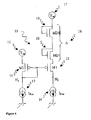
- the arrangement of the first embodiment of the invention shown in fig 4 is provided. This shows a voltage comparator (10) having two inputs, and comprising transistors M1 (12) and M2 (11), two biasing current sources (13 and 14) and an element (16) for generating a reference voltage drop.
- a "reference" input voltage V in1 (15) is connected to a second main electrode, e.g. the source of transistor M2 (11), the first electrode of the element (16) generating a voltage drop being connected to the second main electrode, e.g. source of transistor M1 (12) while its second electrode is connected to a second input voltage V in2 (17).
- the arrangement has two principal current paths, one from the first input through the second main electrode, e.g. source and the first main electrode, e.g. drain of transistor M1 and through current source 13 to ground.
- a second current path passes from the second input though the voltage drop element, through the second main electrode, e.g. source and the first main electrode, e.g. drain of transistor M2, and through the second current source 14 to ground.
- the reference voltage drop can be embodied by, for example, any one of the following or any combination of the following:
- the control electrodes e.g. gates of transistor M1 and M2 are connected together.
- the control electrode, e.g. gate of transistor M2 is connected to the first main electrode, e.g. drain of the same transistor M2.
- VT is the threshold voltage of the transistors, e.g. pMOS transistors M1 and M2.
- ⁇ V is dimensioned so as to take the current mismatch between first and second current path - whether accidental or purposeful - into account. This can be used as the output of the comparator.
- ⁇ V the voltage across the voltage dropping element determines the threshold level at which the transition occurs, relative to the first input. This enables the threshold to be set well above the supply voltage of circuitry following the comparator.
- the first input can use a fixed reference, if the threshold is to be fixed. Or the first input can be variable and the comparator used to detect when the second input exceeds the first input by a predetermined voltage.
- the transistors M1 and M2 can be identical, i.e., having the same W/L ratio (gate width to length ratio), and the current sources can be arranged to provide the same current, to ensure the same current is present in each of the two current paths.
- the transistors and the current sources can be arranged so that the currents in the two current paths differ by a predetermined amount.
- other similar or equivalent circuits can be conceived using NMOS transistors, or using negative voltage supply levels and current flows in reverse to the embodiment shown and so on.
- BiCMOS transistors can be used. Circuits in accordance with the present invention can also be realized using exclusively bipolar transistors.
- the current sources can be implemented using conventional techniques.
- the voltage drop element can be implemented using a resistor and more preferably one or more diode drops or other transistor circuitry following established techniques.
- FIG. 5 shows a voltage monitoring/comparator circuit (200).
- the high-voltage transistors M3 (203) and M4 (204) biased with V aux limit the voltage at nodes N 6 and N 7 .
- a series of transistors (210, 211 and 212) connected in diode can be used.
- the voltage at node N 1 may rise above the voltage at node N 5 : the parasitic diode Dp (207) (between first main electrode, e.g. drain and bulk of transistor M2 201) is then forward biased and a short-circuit occurs.
- the diode DI(208) will prevent this: should the voltage at node N 1 rise above V in1 , D1 is backward biased and no current flows through it.
- the diode D2 (215) is used to compensate for the offset introduced by D 1 (one diode voltage drop).
- the output of the comparator is now node 7, that can be connected to the input of a (low voltage) Schmitt trigger.
- a comparator has first and second current paths, each passing from an input (15,17) through a transistor (M1, M2), through a current source to ground, the second current path also having a reference voltage drop element (16) coupled in series with the second input.
- the gates of the transistors are coupled to form a current mirror.
- the reference voltage drop element enables higher voltages to be input and compared to higher thresholds above an internal supply voltage level without the need for dividing resistors to reduce the input voltage. Avoiding such resistors means the power dissipation and the silicon area used can be kept lower. ESD vulnerability is reduced since the inputs are not coupled to gates of MOS transistors. Overvoltage protection across the source and gate of the second transistor can be added.
- the transistors may be implemented in other technologies such as MOS technologies in general including CMOS and BiCMOS. Bipolar is less preferred.
Landscapes
- Physics & Mathematics (AREA)
- Nonlinear Science (AREA)
- Measurement Of Current Or Voltage (AREA)
Abstract
Description
- Field of the invention: This invention relates to comparators, and to integrated circuits having such comparators, and to devices having such integrated circuits as well as to methods of operating and making these.
- It is known to try to reduce power supply voltages for integrated circuits to reduce power consumption and to allow for increased integrated circuit densities. However, this may result in systems having integrated circuits using digital components powered by different supply voltages, which can cause interfacing problems. For example, transistors in the reduced voltage circuit may be subject to failure if forced to sustain the larger power supply voltage. If these transistors are protected with limiting diodes, this may prevent the transistors from detecting the desired signals, particularly in the case of differential signalling. Circuits such as comparators and differential amplifiers can use differential inputs. US patent 5,942,921 is concerned with this issue and shows a solution for interfacing low voltage circuitry to high voltage circuitry, and in particular, to an interface circuit which operates from the low voltage power supply to detect differential signals which may have signal voltages that exceed the voltage of the low power supply. A first transistor and a first resistor coupled in series are coupled in parallel with a second transistor and a second series resistor. The transistor drain terminals are both coupled to the power supply voltage, and a current source draws current from the common node of the resistors. Input voltages are supplied to the gates of the transistors, and the differential output voltages are provided from the transistor source terminals. A differential amplifier receives the differential output voltages and provides a single output voltage. The differential buffer transistors are exposed to only the differences between the input voltages and the power supply voltage, and consequently may not be subject to failure if the input voltage exceeds the power supply voltage. Further, the current carrying capacity of the transistors is modulated by the input voltages regardless of whether the input voltages exceed the supply voltages or not, thereby allowing differential detection even with signal voltages that exceed the power supply voltage.
- It is also known from French patent publication FR 2 838 840 that comparing a supply voltage with a determined voltage cannot be carried out with a conventional comparator having two inputs and one power supply input since the differential stages of the comparator cannot be biased by the same voltage as one of the voltages to be compared. The solution proposed in this case involves the comparator having first and second PMOS transistors arranged as current mirrors, as shown schematically in fig 2 described in more detail below. The first PMOS transistor has its source connected to the first input of the comparator for receiving the first voltage. The second PMOS transistor has its source connected to the second input of the comparator for receiving the second voltage. The output of the comparator is connected to the drain of one of the transistors. This is useful in specific applications such as control of a charge pump involving compare an internal supply voltage level and an external supply voltage, to determine when the external supply drops below a threshold.
- For other applications of comparators where signals to be compared are both higher than the internal supply voltage, it is known to use resistive dividers/level shifters to reduce the voltages input to the comparator to a level below the internal supply voltage level, and the inputs can be fed to gates of the transistors of the comparator. US patent 5,302,902 shows an example where level sensing uses such resistive scaling. US patent 6,304,088 shows another example in which monitoring of the voltage VBAT requires a resistive divider too. This is described in more detail below with reference to fig 3
- To limit the current dissipated in such resistive dividers, the value of the resistance should be high. This is useful for thermal management of products as well as battery life of mobile products. However this often conflicts or is incompatible with using only a small area of silicon to reduce costs and increase integration levels.
- An object of the invention is to provide improved apparatus or methods, especially comparators, and integrated circuits having such comparators, and devices having such integrated circuits as well as methods of operating and making these.
- According to a first aspect, the invention provides a comparator for comparing voltages of first and second inputs, and having first and second current paths coupled to the first and second inputs respectively, the first current path passing from the first input through a first main electrode such as a drain and second main electrode, e.g. a source of a first transistor, and through a first bias current source to a supply line, the second current path passing through a reference voltage drop element, through a first main electrode, e.g. a drain and a second main electrode, e.g. a source of a second transistor, and through a second bias current source to a supply line. The comparator may be implemented in CMOS or BiCMOS technology, for example and less preferred in bipolar technology. The first and second transistors (M1 and M2) are preferably MOS transistors.
- The comparator is implemented with a current mirror arrangement, but the additional reference voltage drop element enables higher voltages to be input and compared to an internal supply voltage level without the need for resistive dividers. The higher thresholds could be achieved by combining the conventional technique of a differential amplifier arrangement with the conventional voltage dropping resistive dividers on one or both inputs, but at a cost of higher power dissipation, i.e. due to the limitation imposed on the size of integrated resistors. The advantages are based on a recognition that the power dissipation of the comparator is determined by the biasing current sources only, and the area of semiconductor, e.g. silicon used by current sources is usually smaller than the area used by resistors of sufficient resistance to limit the current at the level imposed by these current sources. An additional advantage is that the inputs of the comparator are not connected to control electrodes of transistors, e.g. gates of MOS transistors, which should improve the resistance of the component to ESD. Hence the power dissipation and or the semiconductor, e.g. silicon area used can be kept lower than known arrangements using dividing resistors.
- The reference voltage drop element can include a resistance (less preferred), and or one or more diode drops or other circuitry. In particular, the reference voltage drop can be embodied by, for example, any one or any combination of the following:
- a diode or diodes in series. The diodes are forward biased but the use of reverse biased diodes is included, e.g. for very low currents, such as for use in the femto to nanoampere range. The advantages of diodes are their robustness and small size. This achieves one of the goals of the present invention , e.g. together with low power dissipation.
- diode connected transistors, e.g. MOS transistors with their gate connected to their drain electrode. For a given voltage drop at a given current level, transistors (and diode) will be smaller than resistors.
- a resistor is a less preferred solution since it will always occupy more silicon area than a series of diodes or diode connected transistor for a given current and a given voltage drop.
- a battery, e.g. discrete, is a less a preferred solution. Typically, a battery cannot be integrated on chip in standard technologies. However the present invention includes within its scope the use of batteries, e.g. integration of batteries on-chip in future technologies. For instance Zn/Air batteries can already be printed on paper.
- An additional feature of the present invention is the first and second transistors, e.g. transistors M1 and M2, being PMOS transistors.
- Another such feature is the control electrodes, e.g. gates of the first and second transistors being coupled together. Another such feature is the first main electrodes, e.g. drains of the first and second transistors being coupled to the first and second current sources respectively. The first input is fed to the second main electrode, e.g. source of the first transistor. The second input is applied to one of the electrodes of the voltage drop element. Another such feature is the control electrode, e.g. gate and the first main electrode, e.g. drain of the first transistor being coupled together. Another such feature is the voltage drop element comprising one or more transistors. Another such feature is an output being taken from a first main electrode, e.g. drain of the second transistor.
- Another such feature is a third transistor in the first current path and coupled to the first main electrode, e.g. drain of the first transistor. The third transistor is connected between the first transistor and the current source in the first current path to limit the voltage at the positive electrode of the current source. A fourth transistor can be included in the second current path and coupled to a first main electrode, e.g. drain of the second transistor and the current source in the second current path to limit overvoltage at the positive electrode of the current source. Another such feature is circuitry coupled between the second main electrode, e.g. source, and a control electrode, e.g. gate of the second transistor to limit overvoltage. This is useful for enabling implementation in technologies vulnerable to such overvoltage. Another such feature is a diode coupled to the first input to protect the first input from current flow through forward biasing of a parasitic diode from drain to bulk of the first transistor.
- Another aspect of the invention provides an integrated circuit having the comparator. Another aspect provides a battery powered mobile device having the integrated circuit. This is based on a recognition that the advantages of the integrated circuit can feed through to such devices to improve the device performance.
- Any of the additional features can be combined together and combined with any of the aspects. Other advantages will be apparent to those skilled in the art, especially over other prior art. Numerous variations and modifications can be made without departing from the claims of the present invention. Therefore, it should be clearly understood that the form of the present invention is illustrative only and is not intended to limit the scope of the claims of the present invention.
- How the present invention may be put into effect will now be described by way of example with reference to the appended drawings, in which:
- Figs 1 to 3 show known arrangements,
- Fig 4 shows a schematic view of a comparator according to a first embodiment of the invention, and
- Fig 5 shows a schematic view of a second embodiment.
- Figs. 6 and 7 show schematic views of further embodiments including alternative reference voltage drop means.
- The present invention will be described with respect to particular embodiments and with reference to certain drawings but the invention is not limited thereto but only by the claims. Any reference signs in the claims shall not be construed as limiting the scope. The drawings described are only schematic and are non-limiting. In the drawings, the size of some of the elements may be exaggerated and not drawn on scale for illustrative purposes. Where the term "comprising" is used in the present description and claims, it does not exclude other elements or steps. Where an indefinite or definite article is used when referring to a singular noun e.g. "a" or "an", "the", this includes a plural of that noun unless something else is specifically stated.
- It is furthermore to be noticed that the term "comprising", used in the description and in the claims, should not be interpreted as being restricted to the means listed thereafter; it does not exclude other elements or steps. Thus, the scope of the expression "a device comprising means A and B" should not be limited to devices consisting only of components A and B. It means that with respect to the present invention, the only relevant components of the device are A and B.
- Reference will be made to transistors. These are three-terminal devices: a first main electrode such as a drain, a second main electrode such as a source and a control electrode such as a gate for controlling the follow of electrical charges between the first and second main electrodes.
- For reference, before describing the embodiments, known arrangements will be described briefly. Fig 1 shows a circuit known from US 5,942,921. This includes a differential buffer for a
differential amplifier 202. The differential buffer includes a transistor 402 in series with aresistance 404, coupled in parallel with a second transistor 406 matched to the first (402) and a second resistance 408 equal to the first (404). The common node shared by transistors 402 and 406 is coupled to the supply voltage, and the common node shared by theresistances 404 and 408 is connected to ground via acurrent source 410. The input voltages are provided to the gates of the transistors 402 and 406, and the output voltages are provided to the differential amplifier inputs from the transistor source terminals. The differential buffer protects the differential amplifier from excess input signal voltages. The differential buffer transistors are can be driven by input voltage signals up to twice the power supply voltage, and the differential configuration of the buffer provides for continued differential signal detection at voltages above the power supply voltage. Thecurrent source 410 and theresistances 404 and 408 are chosen so that as long as the difference between the input signal voltages is greater than a few millivolts, the output voltage difference saturates at approximately the power supply voltage. The uniform voltage swing at the input to the differential amplifier then provides for a fixed propagation delay, thereby eliminating sensitivity of the output voltage to the size of input voltage swings. - Fig 2 shows a circuit from FR 2 838 840. The comparator is provided to compare an input voltage V1 and an input voltage V2, and to deliver an output signal CS set to 1 when one of the voltages is higher than the other, or set to 0 in the opposite case. The comparator COMP comprises two PMOS transistors TP1, TP2 having their gates G interconnected. The source S of the transistor TP1 forms the first input of the comparator and receives the voltage V1. The source S of the transistor TP2 forms the second input of the comparator and receives the voltage V2. The bulk of the transistor TP1 is taken to the source potential of the transistor, and therefore receives the voltage V1. The bulk of the transistor TP2 is also taken to the source potential of the transistor, and therefore receives the voltage V2. The output of the comparator, which delivers the signal CS, is connected to the drain of the transistor TP2. The transistors TP1, TP2 are in two branches arranged as current mirrors. The first branch comprises the transistor TP1 in series with a transistor TN1, and the second branch comprises the transistor TP2 in series with a transistor TN2. The transistor TP1 has its gate G connected to its drain D, which is connected to the drain D of the transistor TN1. The drain of the transistor TP2 is connected to the drain of the transistor TN2. The sources of the transistors TN1, TN2 are linked to ground, and the gates of the transistors TN1 and TN2 are biased by a voltage Vref(I). The voltage Vref(I) is delivered by a reference voltage generator, not represented here. The voltage Vref(I) is substantially equal to the threshold voltage of the transistors TN1, TN2 such that the latter operate in a saturated mode and are, as a result, equivalent to current sources.
- The comparator COMP operates as a differential amplifier comparing the source voltages of the transistors TP1 and TP2, i.e., the voltages V1 and V2. When the voltage V2 is lower than the voltage V1, i.e., V2=V1-e wherein e is a non-zero quantity, then the gate voltage of the transistor TP2 is equal to V1-Vt, since it is imposed by the transistor TP1 that is on Vt is the threshold voltage of the transistors TP1, TP2. The source-gate voltage Vsg of the transistor TP2 is therefore equal to:


- Transistor TP2 is on and delivers a greater current than the transistor TP1. Since the drain currents of transistors TN1 and TN2 are assumed to be identical, the output signal CS rises and becomes equal to the voltage V2, i.e., the logic level 1. In summary, the transistor TP2 is blocked and the output CS is 0 when the voltage V2 is lower than V1. The transistor TP2 is on and the output CS is 1 when the voltage V2 is higher than V1. There is no suggestion here of how to enable the input voltages to be much greater than the supply voltage.
- Fig 3 shows another
voltage monitor circuit 60 known from US patent 6,304,088. It can be used to monitor any voltage and provide an output signal indicative of the value or a status of the voltage being monitored. A resistor network of three resistors is employed to scale the battery voltage to provide the desired high and low monitor voltage levels. The resistance of each ofresistors voltage monitor circuit 60. Resistance values forresistors resistors voltage monitor circuit 60 is a single pole-double throw switch.Switch 80 has a first position connecting itsoutput terminal 83 to a voltage terminal coupled tonode 72, which is the low voltage monitor level VLow. Switch 80 has a second position connecting itsoutput terminal 83 to another voltage terminal coupled tonode 74, which is the high voltage monitor level VHigh.Switch output terminal 83 is coupled to a non-inverting input terminal ofcomparator 78. Reference voltage VRef is coupled to an inverting input terminal (node 76) ofcomparator 78.Comparator 78 generates an output signal "Power Good" onoutput lead 88 which is also coupled to aswitch control terminal 86 ofswitch 80. When signal Power Good is at a low logic level,switch 80 is in the second position, connectingswitch output terminal 83 tonode 74. When signal Power Good is at a high logic level,switch 80 is in the first position, connectingswitch output terminal 83 tonode 72. In operation, Signal Power Good provides an indication of the status of the battery charge or the battery voltage to be monitored. - In state of the art components, the designer's goal is to synthesize a given function with the minimum transistor count/the lowest silicon area (cost of silicon) and the minimum power dissipation (power budget). The latter is often incompatible with a low area of semiconductor, e.g. silicon. To enable input voltages higher than the supply voltage to be used, and achieve a better balance between power dissipation and silicon area, than can be achieved using dividing resistors, the arrangement of the first embodiment of the invention shown in fig 4 is provided. This shows a voltage comparator (10) having two inputs, and comprising transistors M1 (12) and M2 (11), two biasing current sources (13 and 14) and an element (16) for generating a reference voltage drop. A "reference" input voltage Vin1 (15) is connected to a second main electrode, e.g. the source of transistor M2 (11), the first electrode of the element (16) generating a voltage drop being connected to the second main electrode, e.g. source of transistor M1 (12) while its second electrode is connected to a second input voltage Vin2 (17). The arrangement has two principal current paths, one from the first input through the second main electrode, e.g. source and the first main electrode, e.g. drain of transistor M1 and through
current source 13 to ground. A second current path passes from the second input though the voltage drop element, through the second main electrode, e.g. source and the first main electrode, e.g. drain of transistor M2, and through the secondcurrent source 14 to ground. - The reference voltage drop can be embodied by, for example, any one of the following or any combination of the following:
- diode(s) in series - see Fig. 7. The diodes are forward biased but the use of reverse biased diodes for very low currents is not excluded, e.g. femto to nanoampere range. The advantages of diodes are their robustness and small size.
This achieves is one of the goals of the present invention , e.g. together with low power dissipation. - diode connected transistors, e.g. MOS transistors with their gate connected to their drain electrode - see Fig. 6. For a given voltage drop at a given current level, transistors (and diode) will be smaller than resistors.
- A resistor is a less preferred solution since it will always occupy more silicon area than a series of diodes or diode connected transistor for a given current and a given voltage drop.
- a battery, e.g. discrete, is a less a preferred solution. Typically, a battery cannot be integrated on chip in standard technologies. However the present invention includes within its scope the use of batteries, e.g. integration of batteries on-chip in future technologies. For instance Zn/Air batteries can already be printed on paper.
- The control electrodes, e.g. gates of transistor M1 and M2 are connected together. The control electrode, e.g. gate of transistor M2 is connected to the first main electrode, e.g. drain of the same transistor M2. As long as the voltage Vin2 is sufficiently high, the voltage at node N2 is close to Vin1 - |VT|, where VT is the threshold voltage of the transistors, e.g. pMOS transistors M1 and M2. When the voltage Vin2 drops below Vin1 + ΔV +|VT|, the voltage at node N2 drops to ground. ΔV is dimensioned so as to take the current mismatch between first and second current path - whether accidental or purposeful - into account. This can be used as the output of the comparator. ΔV, the voltage across the voltage dropping element, determines the threshold level at which the transition occurs, relative to the first input. This enables the threshold to be set well above the supply voltage of circuitry following the comparator. The first input can use a fixed reference, if the threshold is to be fixed. Or the first input can be variable and the comparator used to detect when the second input exceeds the first input by a predetermined voltage. This arrangement including the voltage dropping element can enable the total current used for this comparator to be limited to a fraction of a µA for voltages in the
range 12 to 24 volts for VCC = Vin1 and Vin2 respectively, depending upon transistor technology used, e.g. MOS transistors.
The transistors M1 and M2 can be identical, i.e., having the same W/L ratio (gate width to length ratio), and the current sources can be arranged to provide the same current, to ensure the same current is present in each of the two current paths. Alternatively the transistors and the current sources can be arranged so that the currents in the two current paths differ by a predetermined amount. Of course other similar or equivalent circuits can be conceived using NMOS transistors, or using negative voltage supply levels and current flows in reverse to the embodiment shown and so on. Alternatively, BiCMOS transistors can be used. Circuits in accordance with the present invention can also be realized using exclusively bipolar transistors. However, this can be at the cost of increased power dissipation which is not a preferred embodiment of the present invention.The current sources can be implemented using conventional techniques. The voltage drop element can be implemented using a resistor and more preferably one or more diode drops or other transistor circuitry following established techniques. - To implement the invention in technologies where it is crucial to limit the voltage between the control electrode, e.g. gate and the second main electrode, e.g. source of a transistor, some precautions are useful as shown in the embodiment shown in figure 5. This shows a voltage monitoring/comparator circuit (200). The high-voltage transistors M3 (203) and M4 (204) biased with Vaux, limit the voltage at nodes N6 and N7. In order to limit the potential difference between the control electrode, e.g. gate and the second main electrode, e.g. source of (high-voltage) transistor M1 (202), a series of transistors (210, 211 and 212) connected in diode can be used. The number N (where N>= 1) of these transistors T1 to TN required is a function of the threshold voltage of these transistors and the maximum gate to source voltage that the PMOS can tolerate. A rule of thumb is N >= VGS max / Vthreshold. Because of these transistors (T1 to TN)), the voltage at node N1 may rise above the voltage at node N5: the parasitic diode Dp (207) (between first main electrode, e.g. drain and bulk of transistor M2 201) is then forward biased and a short-circuit occurs. The diode DI(208) will prevent this: should the voltage at node N1 rise above Vin1, D1 is backward biased and no current flows through it. The diode D2 (215) is used to compensate for the offset introduced by D 1 (one diode voltage drop). The output of the comparator is now node 7, that can be connected to the input of a (low voltage) Schmitt trigger.
- As has been described above, a comparator has first and second current paths, each passing from an input (15,17) through a transistor (M1, M2), through a current source to ground, the second current path also having a reference voltage drop element (16) coupled in series with the second input. The gates of the transistors are coupled to form a current mirror. The reference voltage drop element enables higher voltages to be input and compared to higher thresholds above an internal supply voltage level without the need for dividing resistors to reduce the input voltage. Avoiding such resistors means the power dissipation and the silicon area used can be kept lower. ESD vulnerability is reduced since the inputs are not coupled to gates of MOS transistors. Overvoltage protection across the source and gate of the second transistor can be added.
- Other variations can be conceived within the scope of the claims. For example, the transistors may be implemented in other technologies such as MOS technologies in general including CMOS and BiCMOS. Bipolar is less preferred.
Claims (12)
- A comparator for comparing voltages of first and second inputs (15, 17), has first and second current paths coupled to the first and second inputs respectively, the first current path passing from the first input (15) through a first main electrode and a second main electrode of a first transistor (M2), and through a first bias current source (13) to a supply line, the second current path passing through a reference voltage drop element (16), through a first main electrode and a second main electrode of a second transistor (M1), and through a second bias current source (14) to a supply line.
- The comparator of claim 1, the first and second transistors (M2, M1) being PMOS.
- The comparator of claim 2, control electrodes of the first and second transistors (M2, M1) being coupled together.
- The comparator of any preceding claim, first main electrodes of the first and second transistors (M2, M1) being coupled to the first and second current sources respectively, and the first input being coupled to the second main electrode of the first transistor.
- The comparator of claim 4, the first input being coupled to an electrode of the reference voltage drop element.
- The comparator of any preceding claim, a control electrode and a first main electrode of the first transistor (M2) being coupled together.
- The comparator of any preceding claim, an output being taken from a first main electrode of the second transistor (M1).
- The comparator of any preceding claim, having a third transistor (M3) in the first current path and coupled to a first main electrode of the first transistor (M2) and a positive electrode of a current source in the first current path to limit overvoltage at the positive electrode of the current source, and a fourth transistor (M4) in the second current path and coupled to a first main electrode of the second transistor (M1) and a positive electrode of a current source in the second current path to limit overvoltage at the positive electrode of the current source in the second current path.
- The comparator of any preceding claim, having circuitry (T1-TN) coupled between the second main electrode and control electrode of the second transistor (M1) to limit overvoltage.
- The comparator of any preceding claim, having a diode (D1) coupled to the first input to protect the first input from current flow through forward biasing of a parasitic diode from drain to bulk of the first transistor (M2).
- An integrated circuit having the comparator of any preceding claim.
- A battery powered mobile device having the integrated circuit of claim 11.
Priority Applications (2)
| Application Number | Priority Date | Filing Date | Title |
|---|---|---|---|
| EP04078179.1A EP1659690B1 (en) | 2004-11-22 | 2004-11-22 | Comparator for input voltages higher than supply voltage |
| US11/282,574 US7315187B2 (en) | 2004-11-22 | 2005-11-21 | Comparator for input voltages higher than supply voltage |
Applications Claiming Priority (1)
| Application Number | Priority Date | Filing Date | Title |
|---|---|---|---|
| EP04078179.1A EP1659690B1 (en) | 2004-11-22 | 2004-11-22 | Comparator for input voltages higher than supply voltage |
Publications (2)
| Publication Number | Publication Date |
|---|---|
| EP1659690A1 true EP1659690A1 (en) | 2006-05-24 |
| EP1659690B1 EP1659690B1 (en) | 2013-11-06 |
Family
ID=34928676
Family Applications (1)
| Application Number | Title | Priority Date | Filing Date |
|---|---|---|---|
| EP04078179.1A Expired - Lifetime EP1659690B1 (en) | 2004-11-22 | 2004-11-22 | Comparator for input voltages higher than supply voltage |
Country Status (2)
| Country | Link |
|---|---|
| US (1) | US7315187B2 (en) |
| EP (1) | EP1659690B1 (en) |
Cited By (4)
| Publication number | Priority date | Publication date | Assignee | Title |
|---|---|---|---|---|
| CN103513690A (en) * | 2013-10-24 | 2014-01-15 | 苏州贝克微电子有限公司 | Built-in comparator |
| CN103513691A (en) * | 2013-10-24 | 2014-01-15 | 苏州贝克微电子有限公司 | Built-in comparator |
| CN113364436A (en) * | 2021-06-24 | 2021-09-07 | 中颖电子股份有限公司 | Voltage comparison circuit |
| CN117278004A (en) * | 2023-11-21 | 2023-12-22 | 拓尔微电子股份有限公司 | Comparison circuit |
Families Citing this family (15)
| Publication number | Priority date | Publication date | Assignee | Title |
|---|---|---|---|---|
| US20080303556A1 (en) * | 2007-06-08 | 2008-12-11 | Uladzimir Fomin | Power supply ground crossing detection circuit |
| JP5535608B2 (en) * | 2009-12-21 | 2014-07-02 | ラピスセミコンダクタ株式会社 | Voltage change detector |
| US8350599B2 (en) * | 2010-03-18 | 2013-01-08 | Aptus Power Semiconductors | Voltage comparators |
| US9614661B2 (en) * | 2012-04-09 | 2017-04-04 | Atmel Corporation | Differential interface for inter-device communication in a battery management and protection system |
| US9112419B2 (en) * | 2013-07-16 | 2015-08-18 | Rohm Co., Ltd. | AC/DC converter with control circuit that receives rectified voltage at input detection terminal |
| CN103888126A (en) * | 2014-03-04 | 2014-06-25 | 东莞博用电子科技有限公司 | Practical level switching circuit |
| JP6498503B2 (en) * | 2015-04-20 | 2019-04-10 | エイブリック株式会社 | Current detection circuit |
| FR3042876B1 (en) | 2015-10-27 | 2017-12-15 | STMicroelectronics (Alps) SAS | DETECTION OF DISTURBANCES OF A POWER SUPPLY |
| TWI635745B (en) * | 2017-02-21 | 2018-09-11 | 晨星半導體股份有限公司 | Receiver and method for controlling receiver |
| US10833653B1 (en) | 2019-09-23 | 2020-11-10 | International Business Machines Corporation | Voltage sensitive delay |
| US11204635B2 (en) | 2019-09-23 | 2021-12-21 | International Business Machines Corporation | Droop detection using power supply sensitive delay |
| US11281249B2 (en) | 2019-09-23 | 2022-03-22 | International Business Machines Corporation | Voltage sensitive current circuit |
| US11152920B2 (en) * | 2019-09-23 | 2021-10-19 | International Business Machines Corporation | Voltage starved passgate with IR drop |
| CN112557739A (en) * | 2020-12-31 | 2021-03-26 | 无锡思泰迪半导体有限公司 | Power supply state judging device |
| US12493062B2 (en) | 2023-05-31 | 2025-12-09 | Stmicroelectronics International N.V. | Integrated circuit with supply voltage detector |
Citations (5)
| Publication number | Priority date | Publication date | Assignee | Title |
|---|---|---|---|---|
| US6008674A (en) * | 1997-04-11 | 1999-12-28 | Mitsubishi Denki Kabushiki Kaisha | Semiconductor integrated circuit device with adjustable high voltage detection circuit |
| US6031397A (en) * | 1997-02-26 | 2000-02-29 | Kabushiki Kaisha Toshiba | Negative voltage detection circuit offsetting fluctuation of detection level |
| US6411133B1 (en) * | 1999-06-30 | 2002-06-25 | Kabushiki Kaisha Toshiba | Semiconductor device |
| US20030058003A1 (en) * | 2001-09-14 | 2003-03-27 | Wolfgang Horn | Comparator |
| FR2838840A1 (en) * | 2002-04-23 | 2003-10-24 | St Microelectronics Sa | Supply voltage comparator for integrated electronic circuits, uses current mirror circuit with supply voltage connected to one input |
Family Cites Families (6)
| Publication number | Priority date | Publication date | Assignee | Title |
|---|---|---|---|---|
| US5302902A (en) | 1991-04-26 | 1994-04-12 | The United States Of America As Represented By The Secretary Of The Army | Abnormal battery cell voltage detection circuitry |
| US5942921A (en) | 1997-12-19 | 1999-08-24 | Advanced Micro Devices, Inc. | Differential comparator with an extended input range |
| US6133764A (en) * | 1999-01-27 | 2000-10-17 | Motorola, Inc. | Comparator circuit and method |
| US6304088B1 (en) | 1999-05-21 | 2001-10-16 | Micrel Incorporated | Voltage monitor circuit with adjustable hysteresis using a single comparator |
| US6447486B1 (en) * | 1999-07-27 | 2002-09-10 | Dennis R. Tollini | Securing tape assembly |
| US6515538B2 (en) * | 2000-04-19 | 2003-02-04 | Nec Compound Semiconductor Devices, Ltd. | Active bias circuit having wilson and widlar configurations |
-
2004
- 2004-11-22 EP EP04078179.1A patent/EP1659690B1/en not_active Expired - Lifetime
-
2005
- 2005-11-21 US US11/282,574 patent/US7315187B2/en not_active Expired - Lifetime
Patent Citations (5)
| Publication number | Priority date | Publication date | Assignee | Title |
|---|---|---|---|---|
| US6031397A (en) * | 1997-02-26 | 2000-02-29 | Kabushiki Kaisha Toshiba | Negative voltage detection circuit offsetting fluctuation of detection level |
| US6008674A (en) * | 1997-04-11 | 1999-12-28 | Mitsubishi Denki Kabushiki Kaisha | Semiconductor integrated circuit device with adjustable high voltage detection circuit |
| US6411133B1 (en) * | 1999-06-30 | 2002-06-25 | Kabushiki Kaisha Toshiba | Semiconductor device |
| US20030058003A1 (en) * | 2001-09-14 | 2003-03-27 | Wolfgang Horn | Comparator |
| FR2838840A1 (en) * | 2002-04-23 | 2003-10-24 | St Microelectronics Sa | Supply voltage comparator for integrated electronic circuits, uses current mirror circuit with supply voltage connected to one input |
Cited By (6)
| Publication number | Priority date | Publication date | Assignee | Title |
|---|---|---|---|---|
| CN103513690A (en) * | 2013-10-24 | 2014-01-15 | 苏州贝克微电子有限公司 | Built-in comparator |
| CN103513691A (en) * | 2013-10-24 | 2014-01-15 | 苏州贝克微电子有限公司 | Built-in comparator |
| CN113364436A (en) * | 2021-06-24 | 2021-09-07 | 中颖电子股份有限公司 | Voltage comparison circuit |
| CN113364436B (en) * | 2021-06-24 | 2023-11-07 | 中颖电子股份有限公司 | Voltage comparison circuit |
| CN117278004A (en) * | 2023-11-21 | 2023-12-22 | 拓尔微电子股份有限公司 | Comparison circuit |
| CN117278004B (en) * | 2023-11-21 | 2024-02-06 | 拓尔微电子股份有限公司 | Comparison circuit |
Also Published As
| Publication number | Publication date |
|---|---|
| US20060125529A1 (en) | 2006-06-15 |
| US7315187B2 (en) | 2008-01-01 |
| EP1659690B1 (en) | 2013-11-06 |
Similar Documents
| Publication | Publication Date | Title |
|---|---|---|
| EP1659690B1 (en) | Comparator for input voltages higher than supply voltage | |
| US7789558B2 (en) | Thermal sensing circuit using bandgap voltage reference generators without trimming circuitry | |
| EP0305098B1 (en) | Cmos to ecl output buffer | |
| US6995599B2 (en) | Cross-conduction blocked power selection comparison/control circuitry with NTC (negative temperature coefficient) trip voltage | |
| CN100566070C (en) | Charge-discharge control circuit and charge-type power supply unit | |
| US6650520B2 (en) | Power supply reverse bias protection circuit for protecting both analog and digital devices coupled thereto | |
| US7719344B1 (en) | Stabilization component for a substrate potential regulation circuit | |
| CN111693759B (en) | Voltage detector | |
| US9059699B2 (en) | Power supply switching circuit | |
| CN106066419A (en) | Current detection circuit | |
| US20040070901A1 (en) | Electrostatic discharge protection circuit | |
| US6967378B2 (en) | Semiconductor integrated circuit device configured to prevent the generation of a reverse current in a MOS transistor | |
| TW201828601A (en) | Output circuit and method for providing an output current | |
| JP2002261241A (en) | Static electricity protection circuit | |
| US8242809B2 (en) | Comparator circuit | |
| US11249118B2 (en) | Current sensing circuit | |
| US20080084232A1 (en) | Negative voltage detector | |
| JP3704856B2 (en) | Load drive circuit | |
| USRE37876E1 (en) | Power supply switch reference circuitry | |
| EP0786810B1 (en) | Substrate potential detecting circuit | |
| US20190310699A1 (en) | Power management integrated circuit | |
| EP1050106B1 (en) | Reverse current throttling of a mos transistor | |
| US6265932B1 (en) | Substrate control voltage circuit of a semiconductor memory | |
| JP7799594B2 (en) | Semiconductor Devices | |
| HK1000924A1 (en) | Comparator start-up arrangement |
Legal Events
| Date | Code | Title | Description |
|---|---|---|---|
| PUAI | Public reference made under article 153(3) epc to a published international application that has entered the european phase |
Free format text: ORIGINAL CODE: 0009012 |
|
| AK | Designated contracting states |
Kind code of ref document: A1 Designated state(s): AT BE BG CH CY CZ DE DK EE ES FI FR GB GR HU IE IS IT LI LU MC NL PL PT RO SE SI SK TR |
|
| AX | Request for extension of the european patent |
Extension state: AL HR LT LV MK YU |
|
| 17P | Request for examination filed |
Effective date: 20060809 |
|
| AKX | Designation fees paid |
Designated state(s): DE FR GB IT |
|
| 17Q | First examination report despatched |
Effective date: 20070102 |
|
| R17C | First examination report despatched (corrected) |
Effective date: 20080102 |
|
| RAP1 | Party data changed (applicant data changed or rights of an application transferred) |
Owner name: SEMICONDUCTOR COMPONENTS INDUSTRIES, LLC |
|
| GRAP | Despatch of communication of intention to grant a patent |
Free format text: ORIGINAL CODE: EPIDOSNIGR1 |
|
| INTG | Intention to grant announced |
Effective date: 20130712 |
|
| GRAS | Grant fee paid |
Free format text: ORIGINAL CODE: EPIDOSNIGR3 |
|
| GRAA | (expected) grant |
Free format text: ORIGINAL CODE: 0009210 |
|
| AK | Designated contracting states |
Kind code of ref document: B1 Designated state(s): DE FR GB IT |
|
| REG | Reference to a national code |
Ref country code: GB Ref legal event code: FG4D |
|
| REG | Reference to a national code |
Ref country code: DE Ref legal event code: R096 Ref document number: 602004043720 Country of ref document: DE Effective date: 20140102 |
|
| REG | Reference to a national code |
Ref country code: DE Ref legal event code: R097 Ref document number: 602004043720 Country of ref document: DE |
|
| PG25 | Lapsed in a contracting state [announced via postgrant information from national office to epo] |
Ref country code: IT Free format text: LAPSE BECAUSE OF FAILURE TO SUBMIT A TRANSLATION OF THE DESCRIPTION OR TO PAY THE FEE WITHIN THE PRESCRIBED TIME-LIMIT Effective date: 20131106 |
|
| PLBE | No opposition filed within time limit |
Free format text: ORIGINAL CODE: 0009261 |
|
| STAA | Information on the status of an ep patent application or granted ep patent |
Free format text: STATUS: NO OPPOSITION FILED WITHIN TIME LIMIT |
|
| 26N | No opposition filed |
Effective date: 20140807 |
|
| REG | Reference to a national code |
Ref country code: DE Ref legal event code: R097 Ref document number: 602004043720 Country of ref document: DE Effective date: 20140807 |
|
| REG | Reference to a national code |
Ref country code: FR Ref legal event code: PLFP Year of fee payment: 12 |
|
| REG | Reference to a national code |
Ref country code: FR Ref legal event code: PLFP Year of fee payment: 13 |
|
| REG | Reference to a national code |
Ref country code: FR Ref legal event code: PLFP Year of fee payment: 14 |
|
| REG | Reference to a national code |
Ref country code: FR Ref legal event code: PLFP Year of fee payment: 15 |
|
| PGFP | Annual fee paid to national office [announced via postgrant information from national office to epo] |
Ref country code: DE Payment date: 20191021 Year of fee payment: 16 |
|
| PGFP | Annual fee paid to national office [announced via postgrant information from national office to epo] |
Ref country code: FR Payment date: 20191022 Year of fee payment: 16 |
|
| PGFP | Annual fee paid to national office [announced via postgrant information from national office to epo] |
Ref country code: GB Payment date: 20191022 Year of fee payment: 16 |
|
| REG | Reference to a national code |
Ref country code: DE Ref legal event code: R119 Ref document number: 602004043720 Country of ref document: DE |
|
| GBPC | Gb: european patent ceased through non-payment of renewal fee |
Effective date: 20201122 |
|
| PG25 | Lapsed in a contracting state [announced via postgrant information from national office to epo] |
Ref country code: FR Free format text: LAPSE BECAUSE OF NON-PAYMENT OF DUE FEES Effective date: 20201130 |
|
| PG25 | Lapsed in a contracting state [announced via postgrant information from national office to epo] |
Ref country code: GB Free format text: LAPSE BECAUSE OF NON-PAYMENT OF DUE FEES Effective date: 20201122 Ref country code: DE Free format text: LAPSE BECAUSE OF NON-PAYMENT OF DUE FEES Effective date: 20210601 |