EP1659638A1 - Power MOS device and corresponding manufacturing method - Google Patents
Power MOS device and corresponding manufacturing method Download PDFInfo
- Publication number
- EP1659638A1 EP1659638A1 EP05025288A EP05025288A EP1659638A1 EP 1659638 A1 EP1659638 A1 EP 1659638A1 EP 05025288 A EP05025288 A EP 05025288A EP 05025288 A EP05025288 A EP 05025288A EP 1659638 A1 EP1659638 A1 EP 1659638A1
- Authority
- EP
- European Patent Office
- Prior art keywords
- gate
- conductive
- portions
- mos device
- layer
- Prior art date
- Legal status (The legal status is an assumption and is not a legal conclusion. Google has not performed a legal analysis and makes no representation as to the accuracy of the status listed.)
- Granted
Links
Images





Classifications
-
- H—ELECTRICITY
- H10—SEMICONDUCTOR DEVICES; ELECTRIC SOLID-STATE DEVICES NOT OTHERWISE PROVIDED FOR
- H10D—INORGANIC ELECTRIC SEMICONDUCTOR DEVICES
- H10D30/00—Field-effect transistors [FET]
- H10D30/60—Insulated-gate field-effect transistors [IGFET]
- H10D30/64—Double-diffused metal-oxide semiconductor [DMOS] FETs
- H10D30/66—Vertical DMOS [VDMOS] FETs
-
- H—ELECTRICITY
- H10—SEMICONDUCTOR DEVICES; ELECTRIC SOLID-STATE DEVICES NOT OTHERWISE PROVIDED FOR
- H10D—INORGANIC ELECTRIC SEMICONDUCTOR DEVICES
- H10D30/00—Field-effect transistors [FET]
- H10D30/01—Manufacture or treatment
- H10D30/021—Manufacture or treatment of FETs having insulated gates [IGFET]
- H10D30/028—Manufacture or treatment of FETs having insulated gates [IGFET] of double-diffused metal oxide semiconductor [DMOS] FETs
- H10D30/0291—Manufacture or treatment of FETs having insulated gates [IGFET] of double-diffused metal oxide semiconductor [DMOS] FETs of vertical DMOS [VDMOS] FETs
-
- H—ELECTRICITY
- H10—SEMICONDUCTOR DEVICES; ELECTRIC SOLID-STATE DEVICES NOT OTHERWISE PROVIDED FOR
- H10D—INORGANIC ELECTRIC SEMICONDUCTOR DEVICES
- H10D64/00—Electrodes of devices having potential barriers
- H10D64/20—Electrodes characterised by their shapes, relative sizes or dispositions
- H10D64/27—Electrodes not carrying the current to be rectified, amplified, oscillated or switched, e.g. gates
- H10D64/311—Gate electrodes for field-effect devices
- H10D64/411—Gate electrodes for field-effect devices for FETs
- H10D64/511—Gate electrodes for field-effect devices for FETs for IGFETs
- H10D64/517—Gate electrodes for field-effect devices for FETs for IGFETs characterised by the conducting layers
-
- H—ELECTRICITY
- H10—SEMICONDUCTOR DEVICES; ELECTRIC SOLID-STATE DEVICES NOT OTHERWISE PROVIDED FOR
- H10D—INORGANIC ELECTRIC SEMICONDUCTOR DEVICES
- H10D64/00—Electrodes of devices having potential barriers
- H10D64/20—Electrodes characterised by their shapes, relative sizes or dispositions
- H10D64/27—Electrodes not carrying the current to be rectified, amplified, oscillated or switched, e.g. gates
- H10D64/311—Gate electrodes for field-effect devices
- H10D64/411—Gate electrodes for field-effect devices for FETs
- H10D64/511—Gate electrodes for field-effect devices for FETs for IGFETs
- H10D64/517—Gate electrodes for field-effect devices for FETs for IGFETs characterised by the conducting layers
- H10D64/518—Gate electrodes for field-effect devices for FETs for IGFETs characterised by the conducting layers characterised by their lengths or sectional shapes
-
- H—ELECTRICITY
- H10—SEMICONDUCTOR DEVICES; ELECTRIC SOLID-STATE DEVICES NOT OTHERWISE PROVIDED FOR
- H10D—INORGANIC ELECTRIC SEMICONDUCTOR DEVICES
- H10D64/00—Electrodes of devices having potential barriers
- H10D64/20—Electrodes characterised by their shapes, relative sizes or dispositions
- H10D64/27—Electrodes not carrying the current to be rectified, amplified, oscillated or switched, e.g. gates
- H10D64/311—Gate electrodes for field-effect devices
- H10D64/411—Gate electrodes for field-effect devices for FETs
- H10D64/511—Gate electrodes for field-effect devices for FETs for IGFETs
- H10D64/517—Gate electrodes for field-effect devices for FETs for IGFETs characterised by the conducting layers
- H10D64/519—Gate electrodes for field-effect devices for FETs for IGFETs characterised by the conducting layers characterised by their top-view geometrical layouts
-
- H—ELECTRICITY
- H10—SEMICONDUCTOR DEVICES; ELECTRIC SOLID-STATE DEVICES NOT OTHERWISE PROVIDED FOR
- H10D—INORGANIC ELECTRIC SEMICONDUCTOR DEVICES
- H10D64/00—Electrodes of devices having potential barriers
- H10D64/01—Manufacture or treatment
- H10D64/013—Manufacture or treatment of electrodes having a conductor capacitively coupled to a semiconductor by an insulator
- H10D64/01302—Manufacture or treatment of electrodes having a conductor capacitively coupled to a semiconductor by an insulator the insulator being formed after the semiconductor body, the semiconductor being silicon
- H10D64/01304—Manufacture or treatment of electrodes having a conductor capacitively coupled to a semiconductor by an insulator the insulator being formed after the semiconductor body, the semiconductor being silicon characterised by the conductor
- H10D64/01326—Aspects related to lithography, isolation or planarisation of the conductor
- H10D64/0133—Aspects related to lithography, isolation or planarisation of the conductor at least part of the entire electrode being a sidewall spacer, being formed by transformation under a mask or being formed by plating at a sidewall
-
- H—ELECTRICITY
- H10—SEMICONDUCTOR DEVICES; ELECTRIC SOLID-STATE DEVICES NOT OTHERWISE PROVIDED FOR
- H10D—INORGANIC ELECTRIC SEMICONDUCTOR DEVICES
- H10D64/00—Electrodes of devices having potential barriers
- H10D64/20—Electrodes characterised by their shapes, relative sizes or dispositions
- H10D64/27—Electrodes not carrying the current to be rectified, amplified, oscillated or switched, e.g. gates
- H10D64/311—Gate electrodes for field-effect devices
- H10D64/411—Gate electrodes for field-effect devices for FETs
- H10D64/511—Gate electrodes for field-effect devices for FETs for IGFETs
- H10D64/514—Gate electrodes for field-effect devices for FETs for IGFETs characterised by the insulating layers
- H10D64/516—Gate electrodes for field-effect devices for FETs for IGFETs characterised by the insulating layers the thicknesses being non-uniform
Definitions
- the present invention relates to a power electronic device, such as a MOS device, of the type comprising a very high integration of elementary MOS transistors and used in multiple applications both at low and high supply voltage.
- the invention also relates to a method for realising the power electronic MOS device with improved dynamic performances.
- the invention particularly, but not exclusively, relates to a power electronic MOS device and the following description is made with reference to this field of application by way of illustration only.
- MOS devices in fact require the possibility of operating, both at low supply voltage (20-100V) and at high supply voltage(200-1000V), but, however, at higher and higher frequencies next to the megaherzt (MHz).
- Power devices are thus subjected to very high voltage and current gradients during the transients and/or during the switches which make the stresses to the device weakening the same burdensome and reduce its activity period in a drastic way.
- elementary MOS transistors are realised on semiconductor or with polygonal cells or strips and they comprise a body region, which, in the case shown, is of the p type, formed on a suitable substrate, of the n type, and with a source region realised on top.
- the body region together with the source region, forms a channel region covered by an insulating layer, for example a silicon oxide, and by a conductive layer, for example suitably doped polysilicon.
- an insulating layer for example a silicon oxide
- a conductive layer for example suitably doped polysilicon.
- These two insulating and conductive layers represent, for each elementary MOS transistor, the gate dielectric and for the power MOS device they form a biasing mesh also called gate mesh.
- the gate mesh is connected to a terminal called gate pad and it allows to distribute the signals inside the MOS device as well as to turn on and/or off all the elementary MOS transistors composing the power MOS device.
- the gate mesh due to the high polysilicon resistivity (> 10 Ohm/ [square] ), exhibits resistive contributions along the path which depend on the relative position with respect to the gate pad, as highlighted in the circuit of figure 2, this implies that gate resistance value of each elementary transistor also depends on the distance from the gate pad.
- each elementary MOS transistor at each switch of the MOS device, responds with a time constant which, being, as known, a function of the input capacity and of the gate resistance, will be distinct for each MOS transistor.
- the gate resistance is thus an important value because, together with the input capacity of the MOS device, forms an RC circuit whose time constant is one of the most important parameters influencing the switch speed of power electronic MOS devices. These latter, having to operate at higher and higher frequencies, thus require a more and more reduced time constant, thus trying to reduce the gate resistance, making it homogeneous for the entire MOS device so as to ensure a greater reliability in high frequency applications.
- connection buses also called gate fingers, realised in metallic material, so as to connect the gate pad to various points of the gate mesh by "short-circuiting" them, as shown in figure 3 and in the corresponding circuit of figure 4.
- a technique is that of increasing the number of gate fingers so as to intersect the gate mesh in the greatest number of points as possible.
- the main one is that the presence of the gate fingers realised in metallic material reduces the active area of the power MOS device since below the gate fingers it is not possible to integrate the elementary MOS transistors.
- a further known solution to reduce the gate resistance provides the decrease of the gate mesh resistance by integrating there inside a very conductive layer.
- metallic silicides such as for example cobalt silicide (CoSi 2 ), platinum silicide (PtSi), titanium silicide (TiSi 2 ) or tungsten silicide (WSi 2 ), which exhibit a layer resistivity of about a lower magnitude order with respect to that of the polysilicon.
- Figure 6 highlights a pattern in parallel of different elementary MOS transistors which exhibit different gate resistances according to the position wherein they are with respect to the gate pad and to the gate fingers.
- the diagram reported in figure 7 shows how between elementary MOS transistors wherein there exists an unbalance in the resistance value, during the switch step of the MOS device, different wave forms are produced which distribute the current at stake in a non uniform way.
- the current intensity, I2 crossing the slowest component undergoes sudden increases affecting the uniformity of the overall time constant of the electronic MOS device.
- the areas in correspondence with the points A and B although being near the gate finger exhibit a different resistance in series due to the contribution of the gate finger section AB, which could have an even higher weight than one Ohm, with a consequent unbalance between the different areas of the power MOS device.
- the unbalance can also cause current focalisations which can cause the non correct operation and/or the breaking of the power MOS device.
- gate oxides other than silicon dioxide for example using hafnium oxide, aluminium oxide, silicon oxide / silicon nitride multilayers and others.
- a further known technique to reduce the total capacity of the device is that of varying the geometry of the gate oxide; such solution provides the realisation of the gate oxide with two different thicknesses in active area as shown for power VDMOS devices, both with channel n and with channel p, in the US patents n° 6,222,232 and n° 6,326,271 to the same Applicant.
- the gate dielectric exhibits two thicknesses: a thin one realised above the channel region, which allows a low threshold voltage driving, and a thicker one extended to the sole region of the gate/drain capacitor, which allows to significantly reduce the transient capacity of the device and thus also the input capacity.
- the definition procedure of the gate structure in the VDMOS devices mainly requires a thermal growth of a thick silicon oxide film from the underlying substrate, its photolithographic definition in active area regions and a growth of a thin gate oxide film which will surmount the channel.
- Such known technique provides the use of a photolithographic step to define the part of the thick gate electrode in the elementary MOS transistor and it provides a successive and more important photolitographic step to delineate the geometry of the gate electrode.
- Such margin labelled with « 1 » in figure 12 must be sufficiently wide as to ensure that possible misalignments in the photolitographic definition of the gate electrode do not cause the extension of the channel below the thick oxide region in an asymmetrical way, on the other hand.
- the technical problem underlying the present invention is that of devising a power electronic MOS device with a high integration density, thus comprising a plurality of elementary MOS transistors with such a gate structure as to ensure a simultaneous switch and with the same time constant, exhibiting such structural and functional characteristics as to overcome the drawbacks cited with reference to the prior art.
- the solution idea underlying the present invention is that of realising a power MOS device, comprising a plurality of elementary MOS transistors, exhibiting an oxide region with double thickness, comprising a first conductive portion or mesh overlapped onto a part of oxide with greater thickness and a second conductive portion or gate electrode of the elementary MOS transistors overlapped onto a part of oxide with thin thickness and being the two conductive portions placed in electric connection by means of suitable conductive bridges.
- the device 1 comprises a plurality of elementary MOS transistors 2 realised on a silicon plate comprising a semiconductor layer 4 overlapped onto a substrate 3.
- the layer 4 exhibits a first type of conductivity which, in the case highlighted in the figure, is of the N-type while the substrate 3 is of the N+ type.
- the elementary MOS transistors 2 exhibit a body region 10, realised in a second type of conductivity, and a source area 11 contained on top.
- the elementary MOS transistors 2 exhibit gate structures 12 comprising a gate oxide 7, of the type with double thickness, comprising in turn a thick central part 8 and lateral portions 9 with reduced thickness, as better highlighted in figure 13.
- the profile of the gate oxide 7 and in particular of the central part 8 can be various and, in the case shown, it exhibits a squared shape substantially upturned T-like.
- the gate structures 12 comprise first gate conductive portions 13 overlapped onto the lateral portions 9 of the gate oxide 7 to define gate electrodes for the elementary MOS transistors 2.
- These first gate conductive portions 13 can also be realised with a double layer made of polysilicon and of a metallic silcide.
- the gate structures 12, as highlighted in figure 14, comprise a conductive structure or mesh 14 suitable to distribute the signal coming from a gate pad or from a finger, suitably defined on the upper surface of the silicon plate and not highlighted in the figures.
- the conductive mesh 14 advantageously comprises second conductive portions 15 overlapped onto the thick central part 8 of the gate oxide 7 and suitably contained therein, interconnected to each other and to the first conductive portions 13 by a plurality of conductive bridges 16.
- the second conductive portions 15 and the conductive bridges 16 are realised in material such as for example polysilicon and they can be suitably doped.
- the second conductive portions 15 being placed above the central thick part 8 can be made very conductive further to hyper-doping.
- these second conductive portions 15 can be realised in polysilicon suitably dopes for being then, by means of suitable process, transformed, for the whole thickness or only for part thereof, into a metallic silicide 50 as highlighted in the embodiments reported in figures 22 and 23.
- the second conductive portions 15 can be realised, entirely as highlighted in figure 19a, in a metallic layer 28 or, as highlighted in figure 19b, they can be realised in a metallic layer 28 overlapped onto a polysilicon layer 29.
- These realisations allow to improve the conductivity of the conductive mesh 14, without jeopardising the functionality of the gate electrode or first conductive portions 13 being separated therefrom although connected by means of the conductive bridges 16.
- the conductive bridges 16 are transversally arranged between second consecutive conductive portions 15 and they comprise a flat portion 17, overlapped onto the semiconductor layer 4, and curve ends 18 arranged above the first conductive portions 13 of said second consecutive conductive portions 15, thus allowing to connect them electrically.
- each conductive bridge 16 can be partially interrupted or completely eliminated for reducing the capacities associated therewith as highlighted in figure 21.
- the conductive bridges 16 further allow to electrically connect the second conductive portions 15 to the first underlying conductive portions 13 allowing an optimal distribution of the signal coming from the gate pad or from a gate finger to the elementary MOS transistors 2.
- the number and the mutual distance of the conductive bridges 16 allow to influence the speed of the power MOS device 1 and the propagation modes of the signal coming from the gate pad are thus suitably programmed and defined according to the needs.
- an insulating interconnection portion 19 realised in material such as for example oxide, which allows to avoid the electric contact between the two parts.
- one part or the entire insulating interconnection portion 19 can be realised simultaneously with the central part 8 of the gate oxide 7, thus exhibiting such a thickness as to allow an enormous gain on the capacities associated therewith.
- the body regions 10 of the elementary MOS transistors 2 are realised between two consecutive conductive bridges 16, they are insulated the ones from the others and they exhibit a peripheral diffusion below the lateral portions 9 of the gate oxides 7 and of the surrounding conductive bridges 16 to define channel regions 21.
- the power MOS device 1 realised according to the present invention thus exhibits a gate structure 12 allowing to separate the transmission line of the signal in the power MOS device 1 by realising the conductive mesh 14 from the gate electrodes by realising first conductive portions 13.
- a gate oxide 7 with double thickness allows to improve the dynamic operation of the power MOS device.
- each elementary MOS transistor 2 is connected to the gate pad or to a gate finger by means of the conductive structure or mesh 14, which is represented by a resistance given by the series of the resistances Rmesh and Rbridge and which is placed in parallel with the resistance of the first conductive portion 13, or gate electrode, indicated as Rpolgate.
- the elementary MOS transistors 2 placed farther from the gate pad or from the gate finger will be made faster with respect to the a configuration according to the prior art wherein the mesh structure is also the gate electrode of the elementary MOS transistors 2 (R polgate ) as highlighted in figure 15.
- the mesh structure is also the gate electrode of the elementary MOS transistors 2 (R polgate ) as highlighted in figure 15.
- those placed closer to the gate pad or to the finger will be slowed down and this allows to uniform the time constant of the plurality of elementary MOS transistors 2 balancing the dynamic response of the power MOS device 1.
- the invention also relates to a method for realising a power MOS device shown making reference to figures 20a to 20h.
- the power MOS device realised is that shown in figures 22 and 23 and it is of the type comprising a plurality of elementary power MOS transistors 2.
- the realisation method according to the invention includes the following steps:
- the walls of the central part 8 of the gate oxide 7 can be very vertical to allow the formation of suitable polysilicon spacers.
- the interconnection portions 19 can be obtained simultaneously with the central parts 8 by means of the anisotropic etching to the oxide thick layer.
- the method further provides the steps of: depositing, above the layer 4, a conductive layer 40 with thickness of about 2000-8000 A as highlighted in figure 20b.
- the conductive layer 40 realised for example in polysilicon, if necessary for the application, can be suitably doped; providing a photo-masking of the conductive layer 40, by placing a resist 41, to defined a conductive mesh 14 of a gate structure 12 suitable to distribute a signal coming from a gate pad or from a finger, suitably defined on the upper surface of the silicon plate and not highlighted in the figures; anisotropically etching the conductive layer 40 to realise first conductive portions 13, of the gate structure 12, overlapped onto the lateral portions 9 of the gate oxide 7, as highlighted in figure 20c.
- the conductive mesh 14 is of the type comprising a plurality of second conductive portions 15 overlapped onto the central part 8 of the gate oxide 7, and a plurality of conductive bridges 16 overlapped onto the interconnection portions 19.
- an anisotropic etching typology will be suitably used allowing to leave a residue, also called spacer, along the walls of the etched material. This allows to realise said first conductive portions 13 or gate electrodes of the elementary MOS transistors 2 self-aligned.
- the process then includes the step of:
- the gate structure 12 comprises a plurality of first conductive portions 13 overlapped onto the lateral portions 9 of the gate oxide 7 and a conductive structure or mesh 14 which in turn comprises a plurality of second conductive portions 15 overlapped onto the central thick part 8 of the gate oxide 7 and interconnected to each other and to the first conductive portions 13 by a plurality of conductive bridges 16 overlapped onto the interconnection portions 19.
- the conductive bridges 16 exhibit a flat portion 17, arranged transversally between first consecutive conductive portions 13 and two curve ends 18 which are placed above and transversally to said first conductive portions 13 to reach corresponding second conductive portions 15.
- the conductive bridges 16 thus allowing to electrically connect second consecutive conductive portions 15 to each other and to connect them to corresponding first portions 13.
- the method further includes the step of:
- the method then includes the steps of:
- the method includes the following completion steps:
- the method described according to the present invention allows to realise a power MOS device comprising a gate structure allowing to separate the gate electrode of the elementary MOS transistors 2 from the distribution mesh of the signal coming from the gate pad, such arrangement obtained by means of a synergy between the layout of the device and a process sequence.
- the method realised is applied to any MOS device characterised by a double gate oxide thickness on whose thick part a conductive mesh is realised and by a conductive gate separated from said conductive mesh and placed on the thin part of the gate oxide and being the two conductive parts placed in electric connection by means of suitable conductive bridges.
- Main advantage of the power MOS device obtained according to the present invention is that the gate structure allows, on one side, to separate the signal transmission mesh coming from the gate pad from the gate electrode of each elementary MOS transistor and, on the other, it allows, by using a gate oxide with double level, to harmonise the response during the dynamic step of the power MOS device.
- a further advantage of the present invention is that the gate structure or mesh is completely self-aligned to the gate electrode of each elementary MOS transistor being obtained through deposition and etching steps. It is thus simpler to be realised and more precise without the use of alignment between masks.
- a further advantage of a MOS device realised by means of the present invention is the possibility of having a greater flexibility in the control of the gate resistance in relation to the number of the conductive bridges realised and to their mutual distance. In such way, by means of a suitable layout, it is possible to vary the switch speed of the power MOS device as well as the propagation mode of the driving signal according to the needs.
- the present invention allows to distribute the conduction bridges so that each area comprised between two consecutive bridges has the same highest gate resistance value R polgate and a minimal value linearly depending on the distance form the gate pad or, if present, on the gate fingers or fingers.
- a further advantage linked to the separation between the conductive structure or mesh and the gate electrode of the elementary MOS transistors is that in such way the conductive material placed on the central part of the gate oxide can be transformed into a silicide avoiding all the problems linked to the faultiness or mechanical stress of the gate electrode which remains in conductive material such as polysilicon.
- the method proposed for realising the MOS device allows to add or substitute the conduction mesh with a metal which implies enormous advantages on the gate resistance values as highlighted in the diagram of figure 18 which allows to considerably increase the switch speed of the MOS device as well as the harmonisation of the response during the dynamic step.
- the MOS device realised by means of the present invention employs a gate oxide with double thickness in technology VLSI keeping the compatibility with a partial or total silicidising process of the polysilicon.
Landscapes
- Electrodes Of Semiconductors (AREA)
- Metal-Oxide And Bipolar Metal-Oxide Semiconductor Integrated Circuits (AREA)
- Insulated Gate Type Field-Effect Transistor (AREA)
Abstract
Description
- The present invention relates to a power electronic device, such as a MOS device, of the type comprising a very high integration of elementary MOS transistors and used in multiple applications both at low and high supply voltage.
- The invention also relates to a method for realising the power electronic MOS device with improved dynamic performances.
- The invention particularly, but not exclusively, relates to a power electronic MOS device and the following description is made with reference to this field of application by way of illustration only.
- As it is well known, in power electronic devices, in particular in power devices of the MOS type, it is important to have the possibility of operating at higher and higher frequencies maintaining the component reliability high.
- The nowadays uses of MOS devices in fact require the possibility of operating, both at low supply voltage (20-100V) and at high supply voltage(200-1000V), but, however, at higher and higher frequencies next to the megaherzt (MHz).
- Power devices are thus subjected to very high voltage and current gradients during the transients and/or during the switches which make the stresses to the device weakening the same burdensome and reduce its activity period in a drastic way.
- As it is well known some power MOS devices are realised by thousands or millions of elementary MOS transistors placed in parallel and individually contributing to the overall capacity in current of the device.
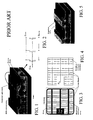
- Typically, elementary MOS transistors, as highlighted in figure 1, are realised on semiconductor or with polygonal cells or strips and they comprise a body region, which, in the case shown, is of the p type, formed on a suitable substrate, of the n type, and with a source region realised on top.
- The body region, together with the source region, forms a channel region covered by an insulating layer, for example a silicon oxide, and by a conductive layer, for example suitably doped polysilicon.
- These two insulating and conductive layers represent, for each elementary MOS transistor, the gate dielectric and for the power MOS device they form a biasing mesh also called gate mesh.
- The gate mesh is connected to a terminal called gate pad and it allows to distribute the signals inside the MOS device as well as to turn on and/or off all the elementary MOS transistors composing the power MOS device.
- The gate mesh, due to the high polysilicon resistivity (> 10 Ohm/[square]), exhibits resistive contributions along the path which depend on the relative position with respect to the gate pad, as highlighted in the circuit of figure 2, this implies that gate resistance value of each elementary transistor also depends on the distance from the gate pad.
- Thus, each elementary MOS transistor, at each switch of the MOS device, responds with a time constant which, being, as known, a function of the input capacity and of the gate resistance, will be distinct for each MOS transistor.
- The gate resistance is thus an important value because, together with the input capacity of the MOS device, forms an RC circuit whose time constant is one of the most important parameters influencing the switch speed of power electronic MOS devices. These latter, having to operate at higher and higher frequencies, thus require a more and more reduced time constant, thus trying to reduce the gate resistance, making it homogeneous for the entire MOS device so as to ensure a greater reliability in high frequency applications.
- To try and solve such problem a known technique is that of carrying out a suitable metallisation of the gate, process consisting in creating connection buses also called gate fingers, realised in metallic material, so as to connect the gate pad to various points of the gate mesh by "short-circuiting" them, as shown in figure 3 and in the corresponding circuit of figure 4.
- A technique is that of increasing the number of gate fingers so as to intersect the gate mesh in the greatest number of points as possible.
- Although advantageous under several aspects, such solution exhibits different drawbacks, the main one is that the presence of the gate fingers realised in metallic material reduces the active area of the power MOS device since below the gate fingers it is not possible to integrate the elementary MOS transistors.
- Moreover, a further drawback linked to the presence of the gate fingers is due to the fact that they limit the number and the position of the wires connecting to the source pad thus affecting negatively the output resistance of the power MOS device.
- A further known solution to reduce the gate resistance provides the decrease of the gate mesh resistance by integrating there inside a very conductive layer. Such process makes use of metallic silicides, such as for example cobalt silicide (CoSi2), platinum silicide (PtSi), titanium silicide (TiSi2) or tungsten silicide (WSi2), which exhibit a layer resistivity of about a lower magnitude order with respect to that of the polysilicon.
- For power electronic MOS devices used in faster and faster applications with low gate resistance, problems however emerge linked to the great voltage and current gradients during the transients.
- All the solution proposed to reduce the gate resistance exhibit the drawback that two elementary MOS transistors placed at different distance from the gate pad are "unbalanced" with respect to each other in the sense that they exhibit two different gate resistance values and thus two different switch speeds. This effect is more and more evident as faster and faster devices are realised.
- Figure 6 highlights a pattern in parallel of different elementary MOS transistors which exhibit different gate resistances according to the position wherein they are with respect to the gate pad and to the gate fingers.
- The diagram reported in figure 7 shows how between elementary MOS transistors wherein there exists an unbalance in the resistance value, during the switch step of the MOS device, different wave forms are produced which distribute the current at stake in a non uniform way. In particular it can be verified how, the current intensity, I2, crossing the slowest component undergoes sudden increases affecting the uniformity of the overall time constant of the electronic MOS device.
- Such behaviour in the power MOS device is exponentially increased for the plurality of elementary MOS transistors, this however jeopardises both the correct functionality and the operating duration of the MOS device itself.
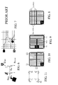
- For the manufacturing process used in the realisation of a power electronic MOS device it is inevitable that there are unbalances in the current progress. In fact it is good to remember that the distance between one gate finger and the other is around values of 200-2000 µm and in such space a lot of elementary MOS transistors are comprised whose gate biasing occurs by means of the gate mesh. In such case the elementary MOS transistors being closer to the gate fingers will be the fastest while the others will be slower and slower, as highlighted in figure 8.
- Further unbalances are due to the fact that for problems due to the assembling step it is complex to realise continuous and equidistant gate fingers (fig. 9). Thus, the power MOS device obtained will exhibit areas with different distances between the gate fingers, as shown in the example of figure 9, and this implies the presence of a gate resistance influenced by the area with lower distance between the gate fingers, since in the calculation of the parallel the areas with higher resistance will have less weight.
- Moreover it is good to reveal that although the resistivity of the material used for realising the gate fingers is low, it is possible that their length is such as to introduce resistive contributions which can be compared with the total gate resistance of the power electronic MOS device especially if, for lowering the metallisation mesh resistance, metallic silicides are used.
- As highlighted in the example of figure 10 and in the associated circuit of figure 11, the areas in correspondence with the points A and B although being near the gate finger exhibit a different resistance in series due to the contribution of the gate finger section AB, which could have an even higher weight than one Ohm, with a consequent unbalance between the different areas of the power MOS device.
- All these causes lead to have power electronic MOS devices weakened by the presence of areas having different gate resistance with consequent negative effects on the switches and during the extreme dynamic stresses with high values of dV/dt and/or dI/dt.
- The unbalance can also cause current focalisations which can cause the non correct operation and/or the breaking of the power MOS device.
- It is also known how in power electronic MOS devices, especially with low voltage driving, for example those driven by means of driver with output voltage 1.8-2.5 Volt, exhibit a more and more reduced thickness of the gate oxide, typically silicon oxide. This reduction allows to obtain threshold voltage values lower that the Volt without deteriorating the breakdown characteristics of the power electronic MOS device.
- However, the reduction of the gate oxide thickness, together with the highest integration density, implies less and less deep junctions and shorter and shorter circuit lengths, with consequent increase of the capacity of the elementary MOS transistors and of the total capacity and with a slowdown of the response speed during the switches.
- To try to reduce the capacity using gate oxides other than silicon dioxide is known for example using hafnium oxide, aluminium oxide, silicon oxide / silicon nitride multilayers and others.
- Changes in the typology of material used however imply drawbacks mainly linked to the necessary tests which require excessively long and prohibitive times for the current market of power electronic MOS devices.
- A further known technique to reduce the total capacity of the device is that of varying the geometry of the gate oxide; such solution provides the realisation of the gate oxide with two different thicknesses in active area as shown for power VDMOS devices, both with channel n and with channel p, in the US patents n° 6,222,232 and n° 6,326,271 to the same Applicant.
- In such proposed solutions the gate dielectric exhibits two thicknesses: a thin one realised above the channel region, which allows a low threshold voltage driving, and a thicker one extended to the sole region of the gate/drain capacitor, which allows to significantly reduce the transient capacity of the device and thus also the input capacity.
- The definition procedure of the gate structure in the VDMOS devices, according to the prior art, mainly requires a thermal growth of a thick silicon oxide film from the underlying substrate, its photolithographic definition in active area regions and a growth of a thin gate oxide film which will surmount the channel.
- Such known technique provides the use of a photolithographic step to define the part of the thick gate electrode in the elementary MOS transistor and it provides a successive and more important photolitographic step to delineate the geometry of the gate electrode.
- Considering that in the elementary MOS transistor there is the need of having a symmetrical and uniform diffused channel using a known procedure for realising power MOS devices with double oxide thickness imposes a margin, with quite high value, between the delimitation of the gate electrode and the edge of the central thick oxide region, as it can be seen in figure 12.
- Such margin labelled with « 1 » in figure 12 must be sufficiently wide as to ensure that possible misalignments in the photolitographic definition of the gate electrode do not cause the extension of the channel below the thick oxide region in an asymmetrical way, on the other hand.
- Obviously, the need of safeguarding the alignment of the planar structures in active area goes against the need of a greater and greater integration of power MOS transistors and thus against the need of operating with more and more reduced dimensions.
- There exist realisations, obtained by using solutions as highlighted for example in the US patent application No. 2002/0140042A1 to the same Applicant, which allow to obtain high integration density devices with self-aligned gate oxide regions. Such realisations, although advantageous under several aspects, exhibit the drawback of significantly reducing the gate mesh in thickness and width and thus they remarkably increase the gate resistance. Moreover, in such known realisations the probelms for introducing a silicide layer inside the gate mesh have significantly increased.
- The technical problem underlying the present invention is that of devising a power electronic MOS device with a high integration density, thus comprising a plurality of elementary MOS transistors with such a gate structure as to ensure a simultaneous switch and with the same time constant, exhibiting such structural and functional characteristics as to overcome the drawbacks cited with reference to the prior art.
- The solution idea underlying the present invention is that of realising a power MOS device, comprising a plurality of elementary MOS transistors, exhibiting an oxide region with double thickness, comprising a first conductive portion or mesh overlapped onto a part of oxide with greater thickness and a second conductive portion or gate electrode of the elementary MOS transistors overlapped onto a part of oxide with thin thickness and being the two conductive portions placed in electric connection by means of suitable conductive bridges.
- On the basis of such solution idea the technical problem is solved by a power electronic MOS device according to
claim 1. - The technical problem is also solved by a method for realising a power MOS device previously indicated and described in the characterising part of
claims 16. - The characteristics and the advantages of the power MOS device and of the method according to the invention will be apparent from the following description of embodiments thereof given by way of indicative and non limiting example making reference to the annexed drawings.
-
- figures 1 to 4 schematically show two embodiments of a power electronic MOS device according to the prior art with the corresponding equivalent circuit;
- figure 5 shows a further embodiment of a power MOS device according to the prior art;
- figures 6 and 7 show an electric circuit and a diagram reporting the wave forms in voltage and current of a turn off of two elementary MOS transistors of a power MOS device realised according to the prior art;
- figures 8 to 10 schematically show the layout of three different embodiments of a MOS device according to the prior art;
- figure 11 shows an equivalent electric circuit of the device of figure 10;
- figure 12 shows a section of an embodiment of a structure with a gate oxide having double thickness according to the prior art;
- figures 13 and 14 show portions of a power MOS device realised according to the present invention respectively in an intermediate process step and once the device is completed;
- figures 15 and 16 show a circuit scheme respectively of a MOS device realised according to the prior art and according to the present invention;
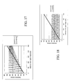
- figures 17 and 18 show two diagrams wherein the resistance as seen from an elementary MOS is represented as function of the distance from a gate finger in a comparison between device realised according to the prior art and according to the present invention;
- figures 19a and 19b show a partial view of two embodiment versions of a MOS device according to the present invention;
- figures 20a to 20h show some steps of the realisation process of a power MOS device according to the present invention;
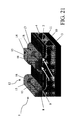
- figure 21 shows a portion of a power MOS device realised according to a further embodiment of the present invention;
- figures 22 and 23 show portions of a power MOS device realised according to the present invention respectively at an intermediate and final completion step.
- With reference to such figures, and in particular to the example of figure 14, 1 globally and schematically indicates a power MOS device realised according to the present invention.
- The
device 1 comprises a plurality ofelementary MOS transistors 2 realised on a silicon plate comprising asemiconductor layer 4 overlapped onto asubstrate 3. Thelayer 4 exhibits a first type of conductivity which, in the case highlighted in the figure, is of the N-type while thesubstrate 3 is of the N+ type. - The
elementary MOS transistors 2 exhibit abody region 10, realised in a second type of conductivity, and asource area 11 contained on top. - Suitably, the
elementary MOS transistors 2exhibit gate structures 12 comprising agate oxide 7, of the type with double thickness, comprising in turn a thickcentral part 8 andlateral portions 9 with reduced thickness, as better highlighted in figure 13. - Naturally, the profile of the
gate oxide 7 and in particular of thecentral part 8 can be various and, in the case shown, it exhibits a squared shape substantially upturned T-like. - Advantageously, the
gate structures 12 comprise first gateconductive portions 13 overlapped onto thelateral portions 9 of thegate oxide 7 to define gate electrodes for theelementary MOS transistors 2. - The first
conductive portions 13, realised in material such as for example polysilicon, flank thecentral part 8 of thegate oxide 7 and they exhibit, in the example of the figures, a substantially rounded profile, naturally they can exhibit any other profile. These first gateconductive portions 13 can also be realised with a double layer made of polysilicon and of a metallic silcide. - Moreover, advantageously, the
gate structures 12, as highlighted in figure 14, comprise a conductive structure ormesh 14 suitable to distribute the signal coming from a gate pad or from a finger, suitably defined on the upper surface of the silicon plate and not highlighted in the figures. - The
conductive mesh 14 advantageously comprises secondconductive portions 15 overlapped onto the thickcentral part 8 of thegate oxide 7 and suitably contained therein, interconnected to each other and to the firstconductive portions 13 by a plurality ofconductive bridges 16. - The second
conductive portions 15 and theconductive bridges 16 are realised in material such as for example polysilicon and they can be suitably doped. - Advantageously, the second
conductive portions 15 being placed above the centralthick part 8 can be made very conductive further to hyper-doping. - In particular, these second
conductive portions 15 can be realised in polysilicon suitably dopes for being then, by means of suitable process, transformed, for the whole thickness or only for part thereof, into ametallic silicide 50 as highlighted in the embodiments reported in figures 22 and 23. - Suitably, the second
conductive portions 15 can be realised, entirely as highlighted in figure 19a, in ametallic layer 28 or, as highlighted in figure 19b, they can be realised in ametallic layer 28 overlapped onto apolysilicon layer 29. These realisations allow to improve the conductivity of theconductive mesh 14, without jeopardising the functionality of the gate electrode or firstconductive portions 13 being separated therefrom although connected by means of the conductive bridges 16. - In fact, the
conductive bridges 16 are transversally arranged between second consecutiveconductive portions 15 and they comprise aflat portion 17, overlapped onto thesemiconductor layer 4, and curve ends 18 arranged above the firstconductive portions 13 of said second consecutiveconductive portions 15, thus allowing to connect them electrically. - Advantageously, the
flat portion 17 of eachconductive bridge 16, can be partially interrupted or completely eliminated for reducing the capacities associated therewith as highlighted in figure 21. - Advantageously, the
conductive bridges 16 further allow to electrically connect the secondconductive portions 15 to the first underlyingconductive portions 13 allowing an optimal distribution of the signal coming from the gate pad or from a gate finger to theelementary MOS transistors 2. - Naturally, the number and the mutual distance of the
conductive bridges 16 allow to influence the speed of thepower MOS device 1 and the propagation modes of the signal coming from the gate pad are thus suitably programmed and defined according to the needs. - Between the
flat portion 17 of theconductive bridges 16 and theunderlying semiconductor layer 4 there is an insulatinginterconnection portion 19, realised in material such as for example oxide, which allows to avoid the electric contact between the two parts. - Advantageously, one part or the entire
insulating interconnection portion 19 can be realised simultaneously with thecentral part 8 of thegate oxide 7, thus exhibiting such a thickness as to allow an incredible gain on the capacities associated therewith. - Suitably, the
body regions 10 of theelementary MOS transistors 2 are realised between two consecutiveconductive bridges 16, they are insulated the ones from the others and they exhibit a peripheral diffusion below thelateral portions 9 of thegate oxides 7 and of the surroundingconductive bridges 16 to definechannel regions 21. - The
power MOS device 1 realised according to the present invention thus exhibits agate structure 12 allowing to separate the transmission line of the signal in thepower MOS device 1 by realising theconductive mesh 14 from the gate electrodes by realising firstconductive portions 13. - Moreover, the use of a
gate oxide 7 with double thickness allows to improve the dynamic operation of the power MOS device. - More in particular, the dynamic response of the
MOS device 1 is improved and balanced, in fact, considering an electric circuit relative to theelementary MOS transistors 2 according to the present invention and reported in figure 16, it is evident how eachelementary MOS transistor 2 is connected to the gate pad or to a gate finger by means of the conductive structure ormesh 14, which is represented by a resistance given by the series of the resistances Rmesh and Rbridge and which is placed in parallel with the resistance of the firstconductive portion 13, or gate electrode, indicated as Rpolgate. - Moreover, being the
conductive mesh 14 arranged above the thickcentral part 8 of thegate oxide 7, this allows that the resistance series Rmesh and Rbridge is always much smaller than the resistance of the gate electrode Rpolgate, thus having a lower weight. - In such way the
elementary MOS transistors 2 placed farther from the gate pad or from the gate finger will be made faster with respect to the a configuration according to the prior art wherein the mesh structure is also the gate electrode of the elementary MOS transistors 2 (Rpolgate) as highlighted in figure 15. Vice versa, those placed closer to the gate pad or to the finger will be slowed down and this allows to uniform the time constant of the plurality ofelementary MOS transistors 2 balancing the dynamic response of thepower MOS device 1. - The invention also relates to a method for realising a power MOS device shown making reference to figures 20a to 20h.
- The realisation steps and the structures described hereafter do not form a complete process flow for the realisation of power MOS devices. In fact the present invention can be put into practice together with the realisation techniques of the MOS devices currently used in the field and hereafter only those steps necessary for the comprehension of the invention are described.
- The power MOS device realised is that shown in figures 22 and 23 and it is of the type comprising a plurality of elementary
power MOS transistors 2. - Hereafter the same above-indicated reference numbers will be used for identifying corresponding parts.
- The realisation method according to the invention includes the following steps:
- making a thick oxide layer with thickness values comprised between 3000-13000 A grow, according to the prior art, from a
semiconductor layer 4 of a silicon plate; - providing a photomasking by means of the placement of a resist 41 on the thick layer for defining a plurality of
gate oxides 7, according to the prior art; - anisotropically etching the thick layer to realise a plurality of
central parts 8 with high thickness; - removing the resist;
- realising an oxide layer with reduced thickness, comprised between 150-1500 A to form
lateral portions 9 of thecentral parts 8 of thegate oxides 7 and to form a plurality ofinterconnection portions 19 transversally connecting thelateral portions 9. - Advantageously, the walls of the
central part 8 of thegate oxide 7 can be very vertical to allow the formation of suitable polysilicon spacers. - Possibly, the
interconnection portions 19 can be obtained simultaneously with thecentral parts 8 by means of the anisotropic etching to the oxide thick layer. The method further provides the steps of: depositing, above thelayer 4, aconductive layer 40 with thickness of about 2000-8000 A as highlighted in figure 20b. Theconductive layer 40, realised for example in polysilicon, if necessary for the application, can be suitably doped;
providing a photo-masking of theconductive layer 40, by placing a resist 41, to defined aconductive mesh 14 of agate structure 12 suitable to distribute a signal coming from a gate pad or from a finger, suitably defined on the upper surface of the silicon plate and not highlighted in the figures;
anisotropically etching theconductive layer 40 to realise firstconductive portions 13, of thegate structure 12, overlapped onto thelateral portions 9 of thegate oxide 7, as highlighted in figure 20c. - Advantageously, the
conductive mesh 14 is of the type comprising a plurality of secondconductive portions 15 overlapped onto thecentral part 8 of thegate oxide 7, and a plurality ofconductive bridges 16 overlapped onto theinterconnection portions 19. - Moreover, an anisotropic etching typology will be suitably used allowing to leave a residue, also called spacer, along the walls of the etched material. This allows to realise said first
conductive portions 13 or gate electrodes of theelementary MOS transistors 2 self-aligned. - The process then includes the step of:
- removing the resist.
- Advantageously according to the present invention the
gate structure 12 comprises a plurality of firstconductive portions 13 overlapped onto thelateral portions 9 of thegate oxide 7 and a conductive structure ormesh 14 which in turn comprises a plurality of secondconductive portions 15 overlapped onto the centralthick part 8 of thegate oxide 7 and interconnected to each other and to the firstconductive portions 13 by a plurality ofconductive bridges 16 overlapped onto theinterconnection portions 19. - Suitably, the
conductive bridges 16 exhibit aflat portion 17, arranged transversally between first consecutiveconductive portions 13 and two curve ends 18 which are placed above and transversally to said firstconductive portions 13 to reach corresponding secondconductive portions 15. Theconductive bridges 16 thus allowing to electrically connect second consecutiveconductive portions 15 to each other and to connect them to correspondingfirst portions 13. - The method further includes the step of:
- forming a plurality of body wells to realise
body regions 10 and source wells to realisesource areas 11 according to the prior art, as highlighted in figure 20c. - In particular the
body regions 10, arranged between aconductive bridge 16 and the successive one, exhibit a peripheral diffusion below saidlateral portions 9 of thegate oxide 7 and of the surroundingconductive bridge 16 to realisechannel regions 21. - Possibly the method then includes the steps of:
- depositing, above the
layer 4, an insulatinglayer 45 of suitable thickness of about 100-5000 A, as shown in figure 20d; - providing a photo-masking of the insulating
layer 45 placed above thegate structure 12 except for the upper part of the secondconductive portions 15, to thus define suitable areas to be silicidised as highlighted in figure 2oe; - depositing, above the second
conductive portions 15, a suitablemetallic layer 46 of thickness equal to approximately 200-5000 A, as shown in figure 20f; - carrying out a thermal process or other process suitable to make the
metallic layer 46 react with an upper portion of the secondconductive portions 15, realised in silicon, which, reacting, define asilicidised layer 50; - etching the
metallic layer 45 by taking away the part which has not reacted, as highlighted in figure 20g; - The method includes the following completion steps:
- covering the structure with a suitable intermediate
dielectric layer 47 and formingmetallisations 48 on the front and on the rest according to the prior art, suitable to obtain a device as shown in figures 20h, 22 and 23. - The method described according to the present invention allows to realise a power MOS device comprising a gate structure allowing to separate the gate electrode of the
elementary MOS transistors 2 from the distribution mesh of the signal coming from the gate pad, such arrangement obtained by means of a synergy between the layout of the device and a process sequence. - The method realised is applied to any MOS device characterised by a double gate oxide thickness on whose thick part a conductive mesh is realised and by a conductive gate separated from said conductive mesh and placed on the thin part of the gate oxide and being the two conductive parts placed in electric connection by means of suitable conductive bridges.
- Main advantage of the power MOS device obtained according to the present invention is that the gate structure allows, on one side, to separate the signal transmission mesh coming from the gate pad from the gate electrode of each elementary MOS transistor and, on the other, it allows, by using a gate oxide with double level, to harmonise the response during the dynamic step of the power MOS device.
- Moreover, a further advantage of the present invention is that the gate structure or mesh is completely self-aligned to the gate electrode of each elementary MOS transistor being obtained through deposition and etching steps. It is thus simpler to be realised and more precise without the use of alignment between masks.
- A further advantage of a MOS device realised by means of the present invention is the possibility of having a greater flexibility in the control of the gate resistance in relation to the number of the conductive bridges realised and to their mutual distance. In such way, by means of a suitable layout, it is possible to vary the switch speed of the power MOS device as well as the propagation mode of the driving signal according to the needs.
- In particular, the present invention allows to distribute the conduction bridges so that each area comprised between two consecutive bridges has the same highest gate resistance value Rpolgate and a minimal value linearly depending on the distance form the gate pad or, if present, on the gate fingers or fingers.
- A further advantage linked to the separation between the conductive structure or mesh and the gate electrode of the elementary MOS transistors is that in such way the conductive material placed on the central part of the gate oxide can be transformed into a silicide avoiding all the problems linked to the faultiness or mechanical stress of the gate electrode which remains in conductive material such as polysilicon.
- From experimental tests carried out by the Applicant it has been possible to verify that the power MOS device realised by means of the present invention is particularly satisfying if the resistance gate seen from the elementary MOS transistors is analysed with respect to all the other techniques currently used in the field. In particular, as it can be seen from the diagram of figure 17, there is a more harmonious progress of the resistance value allowing to balance the response of the device during the dynamic step more.
- Moreover, the method proposed for realising the MOS device allows to add or substitute the conduction mesh with a metal which implies enormous advantages on the gate resistance values as highlighted in the diagram of figure 18 which allows to considerably increase the switch speed of the MOS device as well as the harmonisation of the response during the dynamic step.
- The MOS device realised by means of the present invention employs a gate oxide with double thickness in technology VLSI keeping the compatibility with a partial or total silicidising process of the polysilicon.
- The solution idea of separating the transmission structure of the signal from the gate electrode of the elementary transistors and of interconnecting them by means of suitable conductive bridges can be naturally used also for other electronic devices maintaining similar advantages.
Claims (17)
- Power MOS device of the type comprising a plurality of elementary power MOS transistors (2) having respective gate structures (12) comprising a gate oxide (7) having a thick central part (8) and lateral portions (9) of reduced thickness, characterised in that said gate structures (12) comprise first gate conductive portions (13) overlapped onto said lateral portions (9) of gate oxide (7) as well as a conductive structure or mesh (14) in turn comprising a plurality of second conductive portions (15) overlapped onto the thick central part (8) of gate oxide (7) of each transistor and interconnected to said first gate conductive portions (13) by means of a plurality of conducive bridges (16).
- MOS device according to claim 1, characterised in that said first gate conductive portions (13) are realised in polysilicon and they flank said central part (8) of the gate oxide (7), said first conductive portions (13) representing for each of said elementary MOS transistors (2) a gate electrode.
- MOS device according to claim 1, characterised in that said first gate conductive portions (13) are realised in a double layer made of polysilicon and of a metallic silicide.
- MOS device according to claim 1, characterised in that said conductive bridges (16) are arranged transversally between two consecutive of said second consecutive conductive portions (15) and they comprise a flat portion (17) overlapped onto said semiconductor layer (4) and curve ends (18) arranged above and transversally to said first gate conductive portions (13) allowing to electrically connect said second consecutive conductive portions (15) to each other and to said first underlying gate conductive portions (13).
- MOS device according to claim 4, characterised in that between each of said flat portions (17) of said conductive bridges (16) and said underlying semiconductor layer (4) there is an insulating interconnection portion (19) suitable to avoid an electric contact between such two parts.
- MOS device according to claim 5, wherein said insulating interconnection portion (19) is realised by means of an oxide layer.
- MOS device according to claim 5, wherein said insulating interconnection portion (19) is realised by means of an oxide layer with double thickness.
- MOS device according to claim 1, wherein said conductive bridges 16 comprise curve ends (18) arranged above and transversally to said first gate conductive portions (13) allowing to electrically connect said second upper conductive portions (15) to said first underlying gate conductive portions (13).
- MOS device according to one or more of the preceding claims, characterised in that said second conductive portions (15) and said conductive bridges (16) are realised in material such as polysilicon.
- MOS device according to one or more of the preceding claims, characterised in that said second conductive portions (15) and/or said conductive bridges (16) can be suitably doped.
- MOS device according to claim 1, characterised in that said second conductive portions (15) can be realised in a double layer made of polysilicon and of a metallic silicide.
- MOS device according to claim 1, characterised in that said second conductive portions (15) can be realised in a metallic silicide layer.
- MOS device according to claim 1, characterised in that said second conductive portions (15) can be realised in a metallic layer.
- MOS device according to one or more of the preceding claims, characterised in that said conductive bridges (16) are realised in a predetermined number and arranged at a suitable and variable mutual distance.
- MOS device according to one or more of the preceding claims, characterised in that said elementary MOS transistors (2) exhibit body regions (10) and a source area (11) contained on top, said body regions (10) being realised between two of said consecutive conductive bridges (16) and being insulated the ones from the others exhibiting a peripheral diffusion below said lateral portions (9) of said gate oxides (7) and of said surrounding conductive bridges (16) to define channel regions (21).
- Method for realising a power electronic MOS device comprising the steps of:- making a thick oxide layer grow from a semiconductor layer (4) of a silicon plate;- providing a photo-masking, by placing a resist, on said thick layer to define a plurality of gate oxides (7);- anisotropically etching the thick layer and realising a plurality of central parts (8) with high thickness;- removing the masking;- realising a thinner gate oxide layer with respect to said thick oxide layer to form portions (9) lateral to said central parts (8) and a plurality of insulating interconnection portions (19) transversal with respect to said consecutive gate layers (7);characterised in that said method comprises the steps of:
said gate oxide (7) with double thickness obtained exhibit a thick central part (8) and lateral portions (9) with reduced thickness, and said plurality of insulating interconnection portions (19) connecting said consecutive lateral portions (9) according to a transversal position,- depositing on top of said semiconductor layer (4) a conductive layer;- providing a photo-masking of the conductive layer, by placing a resist (41), to defined a gate structure (12) comprising a conductive mesh (14) of the type comprising a plurality of conductive portions (15) overlapped onto said central part (8) of said gate oxide (7) and a plurality of conductive bridges (16) overlapped onto said interconnection portions (19);- anisotropically etching, with formation of residue, said central part (8) of said gate oxide (7) to define a plurality of first conductive portions (13) overlapped onto said lateral portions (9);- removing the resist (41);
said gate structure (12) comprising said plurality of first conductive portions (13) overlapped onto said lateral portions (9) of said gate oxide (7) and said conductive structure or mesh (14) comprising in turn said plurality of second conductive portions (15) overlapped onto said thick central part (8) of said gate oxide (7) interconnected to each other and onto said first gate conductive portions (13) from said plurality of conductive bridges (16) overlapped onto said transversal interconnection portions (19). - Realising method according to claim 16, characterised in that it further comprises the steps of:- forming a plurality of body wells to realise body regions (10) and source wells to realise source areas (11) said body regions (10), arranged between a conductive bridge (16) and the successive one, exhibiting a peripheral diffusion below said lateral portions (9) of said gate oxide (7) and of said surrounding conductive bridges (16) to realise channel regions (21).
and in that it comprises the steps of:- depositing an insulating layer (40) of suitable thickness;- providing a photo-masking of said insulating layer (40) to define suitable silicidising areas in particular said second conductive portions (15);- depositing a suitable metallic layer (45);- carrying out a thermal process or other process suitable to make said metallic layer (45) react with the uncovered silicon so as to form a silicide layer (50);- etching and eliminating a portion of said non reacted metallic layer (45);- covering said plate with an intermediate dielectric layer (46) and forming metallisations (48) on the front and on the rest of said plate.
Applications Claiming Priority (1)
| Application Number | Priority Date | Filing Date | Title |
|---|---|---|---|
| IT002244A ITMI20042244A1 (en) | 2004-11-19 | 2004-11-19 | MOS POWER ELECTRONIC DEVICE AND RELATED REALIZATION METHOD |
Publications (2)
| Publication Number | Publication Date |
|---|---|
| EP1659638A1 true EP1659638A1 (en) | 2006-05-24 |
| EP1659638B1 EP1659638B1 (en) | 2011-01-12 |
Family
ID=35597212
Family Applications (1)
| Application Number | Title | Priority Date | Filing Date |
|---|---|---|---|
| EP05025288A Expired - Lifetime EP1659638B1 (en) | 2004-11-19 | 2005-11-18 | Power MOS device and corresponding manufacturing method |
Country Status (3)
| Country | Link |
|---|---|
| EP (1) | EP1659638B1 (en) |
| DE (1) | DE602005025846D1 (en) |
| IT (1) | ITMI20042244A1 (en) |
Cited By (1)
| Publication number | Priority date | Publication date | Assignee | Title |
|---|---|---|---|---|
| WO2013090401A1 (en) * | 2011-12-14 | 2013-06-20 | Microchip Technology Incorporated | Self-aligned gate structure for field effect transistor |
Citations (4)
| Publication number | Priority date | Publication date | Assignee | Title |
|---|---|---|---|---|
| US5510281A (en) | 1995-03-20 | 1996-04-23 | General Electric Company | Method of fabricating a self-aligned DMOS transistor device using SiC and spacers |
| JPH0982965A (en) | 1995-07-11 | 1997-03-28 | Yokogawa Electric Corp | Semiconductor device |
| WO1999033119A2 (en) | 1997-12-19 | 1999-07-01 | Koninklijke Philips Electronics N.V. | Power semiconductor devices |
| US20020140042A1 (en) * | 2001-03-28 | 2002-10-03 | International Rectifier Corporation | Ultra low QGD power MOSFET |
-
2004
- 2004-11-19 IT IT002244A patent/ITMI20042244A1/en unknown
-
2005
- 2005-11-18 EP EP05025288A patent/EP1659638B1/en not_active Expired - Lifetime
- 2005-11-18 DE DE602005025846T patent/DE602005025846D1/en not_active Expired - Lifetime
Patent Citations (4)
| Publication number | Priority date | Publication date | Assignee | Title |
|---|---|---|---|---|
| US5510281A (en) | 1995-03-20 | 1996-04-23 | General Electric Company | Method of fabricating a self-aligned DMOS transistor device using SiC and spacers |
| JPH0982965A (en) | 1995-07-11 | 1997-03-28 | Yokogawa Electric Corp | Semiconductor device |
| WO1999033119A2 (en) | 1997-12-19 | 1999-07-01 | Koninklijke Philips Electronics N.V. | Power semiconductor devices |
| US20020140042A1 (en) * | 2001-03-28 | 2002-10-03 | International Rectifier Corporation | Ultra low QGD power MOSFET |
Non-Patent Citations (1)
| Title |
|---|
| PATENT ABSTRACTS OF JAPAN vol. 1997, no. 07 31 July 1997 (1997-07-31) * |
Cited By (1)
| Publication number | Priority date | Publication date | Assignee | Title |
|---|---|---|---|---|
| WO2013090401A1 (en) * | 2011-12-14 | 2013-06-20 | Microchip Technology Incorporated | Self-aligned gate structure for field effect transistor |
Also Published As
| Publication number | Publication date |
|---|---|
| EP1659638B1 (en) | 2011-01-12 |
| ITMI20042244A1 (en) | 2005-02-19 |
| DE602005025846D1 (en) | 2011-02-24 |
Similar Documents
| Publication | Publication Date | Title |
|---|---|---|
| US8420487B2 (en) | Power MOS electronic device and corresponding realizing method | |
| US8637369B2 (en) | Method for manufacturing an integrated power device having gate structures within trenches | |
| TW437066B (en) | Mosgated device with trench structure and remote contact and process for its manufacture | |
| CN101312189B (en) | Optimized layout structure for multi-stage ESD protection circuit integrated with semiconductor power device | |
| US5592006A (en) | Gate resistor for IGBT | |
| US10566324B2 (en) | Integrated gate resistors for semiconductor power conversion devices | |
| US7186592B2 (en) | High performance, integrated, MOS-type semiconductor device and related manufacturing process | |
| EP0730309B1 (en) | A high voltage MOSFET structure with field plate electrode and process for its fabrication | |
| US5115288A (en) | Split-gate EPROM cell using polysilicon spacers | |
| US20110237038A1 (en) | Closed cell configuration to increase channel density for sub-micron planar semiconductor power device | |
| KR19980041853A (en) | Multi-finger mode transistor with reduced gate resistance | |
| US6955970B1 (en) | Process for manufacturing a low voltage MOSFET power device having a minimum figure of merit | |
| KR100397079B1 (en) | Semiconductor device controllable by field effect | |
| JPH09116094A (en) | Diffusion resistor limited by polycrystalline silicon | |
| US5888889A (en) | Integrated structure pad assembly for lead bonding | |
| EP1659638B1 (en) | Power MOS device and corresponding manufacturing method | |
| JP2001284367A (en) | High frequency field effect transistor | |
| WO2007025956A1 (en) | Single-poly eprom device and method of manufacturing | |
| WO2001031711A2 (en) | Vertical insulated gate field-effect device and method of making the same | |
| US4194174A (en) | Method for fabricating ballasted finger electrode | |
| EP1659636B1 (en) | Power MOS semiconductor device | |
| US20040067610A1 (en) | RF semiconductor devices and methods for fabricating the same | |
| CN120711823A (en) | A power discrete device with integrated resistor and its manufacturing method | |
| JPH04245682A (en) | Field effect transistor | |
| JPS61248475A (en) | Semiconductor device |
Legal Events
| Date | Code | Title | Description |
|---|---|---|---|
| PUAI | Public reference made under article 153(3) epc to a published international application that has entered the european phase |
Free format text: ORIGINAL CODE: 0009012 |
|
| AK | Designated contracting states |
Kind code of ref document: A1 Designated state(s): AT BE BG CH CY CZ DE DK EE ES FI FR GB GR HU IE IS IT LI LT LU LV MC NL PL PT RO SE SI SK TR |
|
| AX | Request for extension of the european patent |
Extension state: AL BA HR MK YU |
|
| 17P | Request for examination filed |
Effective date: 20061123 |
|
| AKX | Designation fees paid |
Designated state(s): DE FR GB IT |
|
| 17Q | First examination report despatched |
Effective date: 20070115 |
|
| RAP1 | Party data changed (applicant data changed or rights of an application transferred) |
Owner name: STMICROELECTRONICS SRL |
|
| RIC1 | Information provided on ipc code assigned before grant |
Ipc: H01L 29/78 20060101AFI20100422BHEP Ipc: H01L 29/49 20060101ALN20100422BHEP Ipc: H01L 21/28 20060101ALN20100422BHEP Ipc: H01L 29/423 20060101ALI20100422BHEP Ipc: H01L 21/336 20060101ALI20100422BHEP |
|
| GRAP | Despatch of communication of intention to grant a patent |
Free format text: ORIGINAL CODE: EPIDOSNIGR1 |
|
| GRAS | Grant fee paid |
Free format text: ORIGINAL CODE: EPIDOSNIGR3 |
|
| GRAA | (expected) grant |
Free format text: ORIGINAL CODE: 0009210 |
|
| AK | Designated contracting states |
Kind code of ref document: B1 Designated state(s): DE FR GB IT |
|
| REG | Reference to a national code |
Ref country code: GB Ref legal event code: FG4D |
|
| REF | Corresponds to: |
Ref document number: 602005025846 Country of ref document: DE Date of ref document: 20110224 Kind code of ref document: P |
|
| REG | Reference to a national code |
Ref country code: DE Ref legal event code: R096 Ref document number: 602005025846 Country of ref document: DE Effective date: 20110224 |
|
| PLBE | No opposition filed within time limit |
Free format text: ORIGINAL CODE: 0009261 |
|
| STAA | Information on the status of an ep patent application or granted ep patent |
Free format text: STATUS: NO OPPOSITION FILED WITHIN TIME LIMIT |
|
| 26N | No opposition filed |
Effective date: 20111013 |
|
| REG | Reference to a national code |
Ref country code: DE Ref legal event code: R097 Ref document number: 602005025846 Country of ref document: DE Effective date: 20111013 |
|
| GBPC | Gb: european patent ceased through non-payment of renewal fee |
Effective date: 20111118 |
|
| PG25 | Lapsed in a contracting state [announced via postgrant information from national office to epo] |
Ref country code: GB Free format text: LAPSE BECAUSE OF NON-PAYMENT OF DUE FEES Effective date: 20111118 |
|
| PG25 | Lapsed in a contracting state [announced via postgrant information from national office to epo] |
Ref country code: IT Free format text: LAPSE BECAUSE OF NON-PAYMENT OF DUE FEES Effective date: 20121118 |
|
| PGFP | Annual fee paid to national office [announced via postgrant information from national office to epo] |
Ref country code: FR Payment date: 20131121 Year of fee payment: 9 |
|
| REG | Reference to a national code |
Ref country code: FR Ref legal event code: ST Effective date: 20150731 |
|
| PG25 | Lapsed in a contracting state [announced via postgrant information from national office to epo] |
Ref country code: FR Free format text: LAPSE BECAUSE OF NON-PAYMENT OF DUE FEES Effective date: 20141201 |
|
| REG | Reference to a national code |
Ref country code: DE Ref legal event code: R079 Ref document number: 602005025846 Country of ref document: DE Free format text: PREVIOUS MAIN CLASS: H01L0029780000 Ipc: H10D0030600000 |
|
| PGFP | Annual fee paid to national office [announced via postgrant information from national office to epo] |
Ref country code: DE Payment date: 20241022 Year of fee payment: 20 |
|
| REG | Reference to a national code |
Ref country code: DE Ref legal event code: R071 Ref document number: 602005025846 Country of ref document: DE |