EP1659621A1 - Substrate including a deformation preventing layer - Google Patents
Substrate including a deformation preventing layer Download PDFInfo
- Publication number
- EP1659621A1 EP1659621A1 EP05110914A EP05110914A EP1659621A1 EP 1659621 A1 EP1659621 A1 EP 1659621A1 EP 05110914 A EP05110914 A EP 05110914A EP 05110914 A EP05110914 A EP 05110914A EP 1659621 A1 EP1659621 A1 EP 1659621A1
- Authority
- EP
- European Patent Office
- Prior art keywords
- substrate
- layer
- thickness
- thin film
- film transistor
- Prior art date
- Legal status (The legal status is an assumption and is not a legal conclusion. Google has not performed a legal analysis and makes no representation as to the accuracy of the status listed.)
- Granted
Links
Images


Classifications
-
- H—ELECTRICITY
- H10—SEMICONDUCTOR DEVICES; ELECTRIC SOLID-STATE DEVICES NOT OTHERWISE PROVIDED FOR
- H10D—INORGANIC ELECTRIC SEMICONDUCTOR DEVICES
- H10D30/00—Field-effect transistors [FET]
- H10D30/60—Insulated-gate field-effect transistors [IGFET]
- H10D30/67—Thin-film transistors [TFT]
- H10D30/6758—Thin-film transistors [TFT] characterised by the insulating substrates
-
- H—ELECTRICITY
- H10—SEMICONDUCTOR DEVICES; ELECTRIC SOLID-STATE DEVICES NOT OTHERWISE PROVIDED FOR
- H10P—GENERIC PROCESSES OR APPARATUS FOR THE MANUFACTURE OR TREATMENT OF DEVICES COVERED BY CLASS H10
- H10P14/00—Formation of materials, e.g. in the shape of layers or pillars
- H10P14/20—Formation of materials, e.g. in the shape of layers or pillars of semiconductor materials
- H10P14/34—Deposited materials, e.g. layers
- H10P14/3402—Deposited materials, e.g. layers characterised by the chemical composition
- H10P14/3404—Deposited materials, e.g. layers characterised by the chemical composition being Group IVA materials
- H10P14/3411—Silicon, silicon germanium or germanium
-
- C—CHEMISTRY; METALLURGY
- C23—COATING METALLIC MATERIAL; COATING MATERIAL WITH METALLIC MATERIAL; CHEMICAL SURFACE TREATMENT; DIFFUSION TREATMENT OF METALLIC MATERIAL; COATING BY VACUUM EVAPORATION, BY SPUTTERING, BY ION IMPLANTATION OR BY CHEMICAL VAPOUR DEPOSITION, IN GENERAL; INHIBITING CORROSION OF METALLIC MATERIAL OR INCRUSTATION IN GENERAL
- C23C—COATING METALLIC MATERIAL; COATING MATERIAL WITH METALLIC MATERIAL; SURFACE TREATMENT OF METALLIC MATERIAL BY DIFFUSION INTO THE SURFACE, BY CHEMICAL CONVERSION OR SUBSTITUTION; COATING BY VACUUM EVAPORATION, BY SPUTTERING, BY ION IMPLANTATION OR BY CHEMICAL VAPOUR DEPOSITION, IN GENERAL
- C23C16/00—Chemical coating by decomposition of gaseous compounds, without leaving reaction products of surface material in the coating, i.e. chemical vapour deposition [CVD] processes
- C23C16/02—Pretreatment of the material to be coated
- C23C16/0272—Deposition of sub-layers, e.g. to promote the adhesion of the main coating
-
- H—ELECTRICITY
- H10—SEMICONDUCTOR DEVICES; ELECTRIC SOLID-STATE DEVICES NOT OTHERWISE PROVIDED FOR
- H10P—GENERIC PROCESSES OR APPARATUS FOR THE MANUFACTURE OR TREATMENT OF DEVICES COVERED BY CLASS H10
- H10P14/00—Formation of materials, e.g. in the shape of layers or pillars
- H10P14/20—Formation of materials, e.g. in the shape of layers or pillars of semiconductor materials
- H10P14/29—Formation of materials, e.g. in the shape of layers or pillars of semiconductor materials characterised by the substrates
-
- H—ELECTRICITY
- H10—SEMICONDUCTOR DEVICES; ELECTRIC SOLID-STATE DEVICES NOT OTHERWISE PROVIDED FOR
- H10P—GENERIC PROCESSES OR APPARATUS FOR THE MANUFACTURE OR TREATMENT OF DEVICES COVERED BY CLASS H10
- H10P14/00—Formation of materials, e.g. in the shape of layers or pillars
- H10P14/20—Formation of materials, e.g. in the shape of layers or pillars of semiconductor materials
- H10P14/29—Formation of materials, e.g. in the shape of layers or pillars of semiconductor materials characterised by the substrates
- H10P14/2901—Materials
- H10P14/2923—Materials being conductive materials, e.g. metallic silicides
-
- H—ELECTRICITY
- H10—SEMICONDUCTOR DEVICES; ELECTRIC SOLID-STATE DEVICES NOT OTHERWISE PROVIDED FOR
- H10P—GENERIC PROCESSES OR APPARATUS FOR THE MANUFACTURE OR TREATMENT OF DEVICES COVERED BY CLASS H10
- H10P14/00—Formation of materials, e.g. in the shape of layers or pillars
- H10P14/20—Formation of materials, e.g. in the shape of layers or pillars of semiconductor materials
- H10P14/32—Formation of materials, e.g. in the shape of layers or pillars of semiconductor materials characterised by intermediate layers between substrates and deposited layers
- H10P14/3202—Materials thereof
- H10P14/3238—Materials thereof being insulating materials
Definitions
- the present invention relates to preventing a substrate from being deformed due to thermal stress or deposition stress.
- Recent mobile display devices and flexible display devices which are increasingly demanded, are required to be thin, light, and unbreakable.
- Mobile display devices and flexible display devices can be thin and light by using a thin glass substrate.
- This thin glass substrate cannot be easily handled and accurately aligned and is weak with respect to withstanding external impact.
- a method of using an existing glass substrate and then chemically or mechanically thinning the glass substrate has been adopted. This method, however, is complicated, and the thinned glass substrate is still weak with respect to withstanding external impact. Thus, this method cannot be used in practice.
- a method of using a metal substrate having high thermal resistance and high flexibility has been proposed.
- the resultant metal substrate is deformed due to a difference between thermal expansion coefficients of the substrate and the layer.
- the thermal expansion coefficient of the layer is greater than that of the metal substrate, the metal substrate is convex in a direction of the layer.
- the thermal expansion coefficient of the metal substrate is greater than that of the layer, the metal substrate is convex in the direction opposite to the direction of the layer.
- this problem can occur not only using a metal substrate but can also occur using other substrates.
- the present invention provides a substrate that is prevented from being deformed due to thermal stress or deposition stress.
- a substrate comprising: a thin film transistor arranged on one surface of the substrate; and a deformation preventing layer, arranged on another surface of the substrate, and including at least one layer.
- the substrate preferably further comprises a planarization layer arranged on the one surface of the substrate, wherein the thin film transistor is arranged on the planarization layer, and the deformation preventing layer is of the same material and thickness as a material and thickness of the planarization layer.
- the planarization layer preferably comprises silicon oxide.
- the substrate preferably further comprises: a planarization layer arranged on the one surface of the substrate; and a buffer layer arranged on the planarization layer, wherein the thin film transistor is arranged on the buffer layer, and the deformation preventing layer includes a first layer of the same material and thickness as the material and thickness of the planarization layer and a second layer formed of the same material and thickness as the material and thickness of the buffer layer.
- the planarization layer preferably comprises silicon oxide.
- the substrate preferably further comprises a protective film arranged on the entire area of the one surface of the substrate to cover the thin film transistor.
- the deformation preventing layer preferably is of the same material and thickness as a material and thickness of the protective film.
- the substrate preferably further comprises a planarization layer arranged on the one surface of the substrate, wherein the thin film transistor is arranged on the planarization layer, and the deformation preventing layer includes a first layer of the same material and thickness as the material and thickness of the planarization layer and a third layer of the same material and thickness as the material and thickness of the protective film.
- the planarization layer comprises silicon oxide.
- the substrate preferably further comprises: a planarization layer arranged on the one surface of the substrate; and a buffer layer arranged on the planarization layer, wherein the thin film transistor is arranged on the buffer layer, and the deformation preventing layer includes a first layer of the same material and thickness as the material and thickness of the planarization layer, a second layer of the same material and thickness as the material and thickness of the buffer layer, and a third layer of the same material and thickness as the material and thickness of the protective film.
- the planarization layer preferably comprises silicon oxide.
- the deformation preventing layer is preferably arranged on the one surface of the substrate and includes layers of the same material and thickness as layers formed on the entire area of the one surface of the substrate.
- the substrate preferably comprises a metal substrate.
- a laminated substrate comprising: a substrate; and a deformation preventing layer arranged on one surface of the substrate.
- the laminated substrate preferably further comprising a planarization layer arranged on another surface of the substrate.
- the deformation preventing layer is preferably of the same material and thickness as a material and thickness of the planarization layer.
- the planarization layer preferably comprises silicon oxide.
- the substrate preferably comprises a metal substrate.
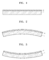
- FIG. 1 is a schematic cross-section of a stack of two layers having different thermal expansion coefficients
- FIGS. 2 and 3 are schematic cross-sections of the layer stack of FIG. 1 deformed by a thermal stress
- FIG. 4 is a schematic cross-section of a substrate including a thin film transistor, according to an embodiment of the present invention.
- FIG. 5 is a schematic cross-section of a metal substrate having a planarization layer formed thereon;
- FIG. 6 is a schematic cross-section of a substrate including a thin film transistor, according to another embodiment of the present invention.
- FIG. 7 is a schematic cross-section of a substrate including a thin film transistor, according to another embodiment of the present invention.
- FIG. 8 is a schematic cross-section of a substrate including a thin film transistor, according to another embodiment of the present invention.
- FIG. 9 is a schematic cross-section of a substrate including a thin film transistor, according to another embodiment of the present invention.
- FIG. 10 is a schematic cross-section of a substrate including a thin film transistor, according to another embodiment of the present invention.
- FIG. 11 is a schematic cross-section of a substrate including a thin film transistor, according to another embodiment of the present invention.
- Mobile display devices and flexible display devices can be thin and light by using a thin glass substrate.
- This thin glass substrate cannot be easily handled and accurately aligned and is weak with respect to withstanding external impact.
- FIG. 4 is a schematic cross-section of a substrate 110 including a thin film transistor 120, according to an embodiment of the present invention.
- the thin film transistor 120 is formed on one surface of the substrate 110, and a deformation preventing layer 101 including at least one layer is formed on the other surface of the substrate 110.
- the substrate 110 can be a metal substrate or a substrate of other various materials.
- the thin film transistor 120 includes a gate electrode 121, which is formed of MoW, etc., a source electrode 122 and a drain electrode 123, which are insulated from the gate electrode 121, and a semiconductor layer 124, which is insulated from the gate electrode 121 and contacts the source electrode 122 and the drain electrode 123.
- a gate insulation film 130 is arranged between the semiconductor layer 124 and the gate electrode 121.
- the source electrode 122 and the drain electrode 123 can be insulated from the gate electrode 121 with an interlayer insulation film 140.
- a polycrystalline silicon layer can be used as the semiconductor layer 124.
- the polycrystalline silicon layer is produced through a crystallization process of transforming an amorphous silicon layer into a polycrystalline silicon layer. Examples of a crystallization process corresponding to a low-temperature process include laser annealing, Metal-Induced Crystallization (MIC), etc.
- the polycrystalline silicon layer is usually produced using an eximer laser annealing method of melting an amorphous silicon layer using a laser and then simultaneously cooling the melted amorphous silicon layer and growing grains or using a sequential lateral solidification method based on the fact that polycrystalline silicon grains grow vertically from a boundary between a liquid area of the amorphous silicon layer irradiated by laser and a solid area thereof not irradiated by laser.
- a process of forming a thin film transistor on a substrate is a high-temperature process, and particularly, such crystallization processes are high-temperature processes. Hence, deformation due to heat, exfoliation of layers, etc. can occur during the manufacture of a thin film transistor.
- the substrate 110 can be curved by thermal stress in a direction closer to the thin film transistor 120 or in the opposite direction. Accordingly, the curving can be prevented by applying a stress to the substrate 110 in the direction opposite to the direction where the thermal stress is applied.
- the deformation preventing layer 101 is formed of a material having a smaller thermal expansion coefficient than the substrate 110 on the other surface of the substrate 110, so that deformation of the substrate 110 due to a thermal stress can be prevented. Also, when the substrate 110 has no deformation preventing layer 101 formed thereon and is bent in the direction becoming farther from the thin film transistor 120 formed on one surface of the substrate 110 similarly to what is shown in FIG.
- the deformation preventing layer 101 is formed of a material having a larger thermal expansion coefficient than the substrate 110 on the other surface of the substrate 110, so that deformation of the substrate 110 due to a thermal stress can be prevented. That is, the material and thickness of the deformation prevention layer 101 can be adequately selected according to a direction and degree in which the substrate 110 is bent, so that deformation of the substrate 110 can be prevented. The prevention of deformation of the substrate 110 helps to prevent detachment between layers, etc.
- processes subsequent to the formation of the thin film transistor 120 on the substrate 110 can also be high-temperature processes, deformation of the substrate 110 or detachment between layers can occur due to a difference between thermal expansion coefficients of the layers. However, they can be prevented by the deformation prevention layer 101 formed on the other surface of the substrate 110.
- FIG. 5 is a schematic cross-section of a metal substrate 210 having a planarization layer 212 formed thereon.
- FIG. 6 is a schematic cross-section of the metal substrate 210 including a thin film transistor 220, according to another embodiment of the present invention.
- the metal substrate 210 has high flexibility and high heat resistance. As shown in FIG. 5, one surface of the metal substrate 210 is very rough, so it needs to be planarized before forming a thin film transistor or the like thereon.
- the planarization can be performed by first chemically or mechanically polishing the rough surface of the metal substrate 210 and then forming the planarization layer 212 on the polished surface of the metal substrate 210.
- the planarization layer 212 has a thickness of about 5000 to 10000 ⁇ , so it has an internal stress.
- the planarization layer 212 is formed of a silicon oxide material having a small internal stress. This preference is equally applied to the following embodiments.
- the planarization layer 212 expands with a thermal stress, so it has a different thermal expansion coefficient from the substrate 210.
- the thermal expansion coefficient difference causes a deformation of the substrate 210.
- the substrate 210 must undergoes a high temperature process, so it is important to minimize the deformation due to the difference between the thermal expansion coefficients of the planarization layer 212 and the substrate 210. This deformation can be prevented by forming a deformation preventing layer 202 on the other surface of the substrate 210.
- the material and thickness of the deformation preventing layer are preferably the same as those of the planarization layer 212, because a deformation of the substrate 210 caused by the difference between the thermal expansion coefficients of the planarization layer 212 and the substrate 210 can be prevented by applying a stress of the same size as a thermal stress applied to the substrate 210 to the substrate 210 in the direction opposite to the direction where the thermal stress is applied.
- FIG. 7 is a schematic cross-section of a substrate 310 including a thin film transistor 320, according to another embodiment of the present invention.
- the substrate 310 in this embodiment is different from the substrate 210 of FIG. 6 in that a buffer layer 314 is formed on a planarization layer 312, which is formed on one surface of the substrate 310, and that a deformation preventing layer formed on the other surface of the substrate 310 includes a first layer 302 and a second layer 304.
- the first layer 302 serves as a layer formed to offset a thermal stress produced due to a distance between thermal expansion coefficients of the planarization layer 312 and the substrate 310.
- the thin film transistor 320 controls signals flowing between a source electrode 322 and a drain electrode 323 according to a signal applied to a gate electrode 321.
- a semiconductor layer 324 in which a channel between the source and drain electrodes 322 and 323 is formed should be protected from external contaminants.
- a buffer layer 314 is formed below the semiconductor 324.
- a thermal stress produced due to a difference between thermal expansion coefficients of the buffer layer 314 and the substrate 310 can be applied to the substrate 310 again.
- the second layer 304 offsets the thermal stress.
- the first layer 302 is used to offset the thermal stress produced due to the planarization layer 312
- the first layer 302 is preferably formed of the same material and to the same thickness as the planarization layer 312.
- the second layer 304 is used to offset the thermal stress produced due to the buffer layer 314, the second layer 304 is preferably formed of the same material and to the same thickness as the buffer layer 314.
- FIG. 8 is a schematic cross-section of a substrate 410 including a thin film transistor 420, according to another embodiment of the present invention.
- a protective film 450 can be included to cover the thin film transistor 420 formed on one surface of the substrate 410.
- the protective film 450 planarizes the upper surface of the thin film transistor 420 prior to forming various component parts on the thin film transistor 420.
- the formation of various component parts on the thin film transistor 420 can be a high temperature process.
- a deformation of the substrate 410, detachment among layers, etc. can occur due to a difference between thermal expansion coefficients of the protective film 450 and the substrate 410.
- a deformation preventing layer 405 is formed to offset a thermal stress produced due to the difference between the thermal expansion coefficients of the protective film 450 and the substrate 410.
- the material and thickness of the deformation preventing layer 405 are preferably the same as those of the protective film 450.
- a protective film can be applied to a substrate structure as illustrated in FIG. 6.
- a protective film can be formed on a thin film transistor formed on a planarization layer formed on one surface of a substrate.
- a first layer 502 and a third layer 505 corresponding to a planarization layer 512 and a protective film 550, respectively, serve as a deformation preventing layer, thus preventing deformation of a substrate 510, detachment among layers, etc.
- Such a protective film can also be applied to a substrate structure as illustrated in FIG. 7.
- a protective film can be formed on a thin film transistor formed on a buffer layer on a planarization layer formed on one surface of a substrate.
- a first layer 602, a second layer 604, and a third layer 605 corresponding to a planarization layer 612m a buffer layer 614, and a protective film 650, respectively, serve as a deformation preventing layer, thus preventing deformation of a substrate 610, detachment among layers, etc.
- FIG. 11 is a schematic cross-section of a substrate 710 including a thin film transistor 720, according to another embodiment of the present invention.
- the thin film transistor 720 is formed on one surface of the substrate 710, and a deformation preventing layer including two layers 703 and 704 is formed on the other surface thereof.
- the reason why the deformation preventing layer includes the two layers 703 and 704 is that layers formed on the entire area of the one surface of the substrate 710 are two, namely, a gate insulation film 730 and an interlayer insulation film 740.
- a deformation of a substrate due to a thermal expansion coefficient difference as described above is mainly due to a difference between thermal expansion coefficients of the substrate and each layer formed on the entire surface of the substrate. Accordingly, it is preferable that a deformation prevention layer including layers corresponding to the layers formed on the entire surface of the substrate is included to offset thermal stresses produced due to differences between the substrate and the thermal expansion coefficients of the layers formed on the entire surface of the substrate.
- the layers included in the deformation preventing layer are preferably formed of the same materials and to the same thicknesses as those of the layers formed on the entire surface of the substrate.
- the deformation preventing layer can be formed on one surface of a substrate having no thin film transistors. In this case, deformation of the substrate, etc. can be prevented even when the substrate including the deformation preventing layer formed on one surface thereof undergoes high-temperature processes.
- all of the elements described in the above-described embodiments can be applied to the substrate that has no thin film transistors and has a deformation preventing layer formed on one surface thereof.
- a planarization layer is formed on the other surface of the substrate, and the deformation preventing layer is formed of the same material and to the same thickness as those of the planarization layer.
- a substrate having no thin film transistors and a substrate having a thin film transistor according to the present invention can have the following effects.
- a deformation preventing layer is formed on the other surface of the substrate, thus preventing deformation of the substrate or detachment between layers caused by heat generated during transformation of an amorphous silicon layer into a polycrystalline silicon layer to manufacture the thin film transistor.
- the deformation preventing layer can also prevent deformation of the substrate or detachment between layers caused by a difference between thermal expansion coefficients of layers that can be generated during processes subsequent to formation of the thin film transistor on the substrate.
- a deformation preventing layer is formed on one surface of the substrate, thus preventing the substrate from being deformed while undergoing a high temperature process.
Landscapes
- Chemical & Material Sciences (AREA)
- General Chemical & Material Sciences (AREA)
- Chemical Kinetics & Catalysis (AREA)
- Engineering & Computer Science (AREA)
- Materials Engineering (AREA)
- Mechanical Engineering (AREA)
- Metallurgy (AREA)
- Organic Chemistry (AREA)
- Thin Film Transistor (AREA)
Abstract
Description
- This application makes reference to, incorporates the same herein, and claims all benefits accruing under 35 U.S.C. §119 from an application for SUBSTRATE AND SUBSTRATE WITH THIN FILM TRANSISTOR earlier filed in the Korean Intellectual Property Office on 20 November 2004 and there duly assigned Serial No. 10-2004-0095535.
- The present invention relates to preventing a substrate from being deformed due to thermal stress or deposition stress.
- Recent mobile display devices and flexible display devices, which are increasingly demanded, are required to be thin, light, and unbreakable.
- Mobile display devices and flexible display devices can be thin and light by using a thin glass substrate. This thin glass substrate cannot be easily handled and accurately aligned and is weak with respect to withstanding external impact. To solve these problems, a method of using an existing glass substrate and then chemically or mechanically thinning the glass substrate has been adopted. This method, however, is complicated, and the thinned glass substrate is still weak with respect to withstanding external impact. Thus, this method cannot be used in practice.
- To solve these problems resulting from the use of glass substrates, a method of using a plastic substrate that is more flexible than the glass substrates and not easily damaged by external impact has been used. However, this plastic substrate has a low thermal resistance, so it cannot bear a high-temperature process, such as, a formation of a polycrystalline silicon thin film transistor and other depositions.
- To solve these problems, a method of using a metal substrate having high thermal resistance and high flexibility has been proposed. However, when a layer is deposited on a metal substrate and the resultant metal substrate undergoes a high-temperature process, the resultant metal substrate is deformed due to a difference between thermal expansion coefficients of the substrate and the layer. For example, when the thermal expansion coefficient of the layer is greater than that of the metal substrate, the metal substrate is convex in a direction of the layer. To the contrary, when the thermal expansion coefficient of the metal substrate is greater than that of the layer, the metal substrate is convex in the direction opposite to the direction of the layer. Of course, this problem can occur not only using a metal substrate but can also occur using other substrates.
- The present invention provides a substrate that is prevented from being deformed due to thermal stress or deposition stress.
- According to one aspect of the present invention, a substrate is provided comprising: a thin film transistor arranged on one surface of the substrate; and a deformation preventing layer, arranged on another surface of the substrate, and including at least one layer.
- The substrate preferably further comprises a planarization layer arranged on the one surface of the substrate, wherein the thin film transistor is arranged on the planarization layer, and the deformation preventing layer is of the same material and thickness as a material and thickness of the planarization layer.
- The planarization layer preferably comprises silicon oxide.
- The substrate preferably further comprises: a planarization layer arranged on the one surface of the substrate; and a buffer layer arranged on the planarization layer, wherein the thin film transistor is arranged on the buffer layer, and the deformation preventing layer includes a first layer of the same material and thickness as the material and thickness of the planarization layer and a second layer formed of the same material and thickness as the material and thickness of the buffer layer.
- The planarization layer preferably comprises silicon oxide.
- The substrate preferably further comprises a protective film arranged on the entire area of the one surface of the substrate to cover the thin film transistor.
- The deformation preventing layer preferably is of the same material and thickness as a material and thickness of the protective film.
- The substrate preferably further comprises a planarization layer arranged on the one surface of the substrate, wherein the thin film transistor is arranged on the planarization layer, and the deformation preventing layer includes a first layer of the same material and thickness as the material and thickness of the planarization layer and a third layer of the same material and thickness as the material and thickness of the protective film.
- The planarization layer comprises silicon oxide.
- The substrate preferably further comprises: a planarization layer arranged on the one surface of the substrate; and a buffer layer arranged on the planarization layer, wherein the thin film transistor is arranged on the buffer layer, and the deformation preventing layer includes a first layer of the same material and thickness as the material and thickness of the planarization layer, a second layer of the same material and thickness as the material and thickness of the buffer layer, and a third layer of the same material and thickness as the material and thickness of the protective film.
- The planarization layer preferably comprises silicon oxide.
- The deformation preventing layer is preferably arranged on the one surface of the substrate and includes layers of the same material and thickness as layers formed on the entire area of the one surface of the substrate.
- The substrate preferably comprises a metal substrate.
- According to another aspect of the present invention, a laminated substrate is provided comprising: a substrate; and a deformation preventing layer arranged on one surface of the substrate.
- The laminated substrate preferably further comprising a planarization layer arranged on another surface of the substrate.
- The deformation preventing layer is preferably of the same material and thickness as a material and thickness of the planarization layer.
- The planarization layer preferably comprises silicon oxide.
- The substrate preferably comprises a metal substrate.
- A more complete appreciation of the present invention and many of the attendant advantages thereof, will be readily apparent as the present invention becomes better understood by reference to the following detailed description when considered in conjunction with the accompanying drawings in which like reference symbols indicate the same or similar components, wherein:
- FIG. 1 is a schematic cross-section of a stack of two layers having different thermal expansion coefficients;
- FIGS. 2 and 3 are schematic cross-sections of the layer stack of FIG. 1 deformed by a thermal stress;
- FIG. 4 is a schematic cross-section of a substrate including a thin film transistor, according to an embodiment of the present invention;
- FIG. 5 is a schematic cross-section of a metal substrate having a planarization layer formed thereon;
- FIG. 6 is a schematic cross-section of a substrate including a thin film transistor, according to another embodiment of the present invention;
- FIG. 7 is a schematic cross-section of a substrate including a thin film transistor, according to another embodiment of the present invention;
- FIG. 8 is a schematic cross-section of a substrate including a thin film transistor, according to another embodiment of the present invention;
- FIG. 9 is a schematic cross-section of a substrate including a thin film transistor, according to another embodiment of the present invention;
- FIG. 10 is a schematic cross-section of a substrate including a thin film transistor, according to another embodiment of the present invention; and
- FIG. 11 is a schematic cross-section of a substrate including a thin film transistor, according to another embodiment of the present invention.
- Mobile display devices and flexible display devices can be thin and light by using a thin glass substrate. This thin glass substrate cannot be easily handled and accurately aligned and is weak with respect to withstanding external impact.
- To solve these problems, a method of using a metal substrate having high thermal resistance and high flexibility has been proposed. However, when a
layer 2 is deposited on ametal substrate 1 and theresultant metal substrate 1 undergoes a high-temperature process, as shown in FIG. 1, theresultant metal substrate 1 is deformed due to a difference between thermal expansion coefficients of thesubstrate 1 and thelayer 2. For example, when the thermal expansion coefficient of thelayer 2 is greater than that of themetal substrate 1, as shown in FIG. 2, themetal substrate 1 is convex in a direction of thelayer 2. To the contrary, when the thermal expansion coefficient of themetal substrate 1 is greater than that of thelayer 2, as shown in FIG. 3, themetal substrate 1 is convex in the direction opposite to the direction of thelayer 2. Of course, this problem can occur not only using a metal substrate but can also occur using other substrates. - FIG. 4 is a schematic cross-section of a
substrate 110 including athin film transistor 120, according to an embodiment of the present invention. Referring to FIG. 4, thethin film transistor 120 is formed on one surface of thesubstrate 110, and adeformation preventing layer 101 including at least one layer is formed on the other surface of thesubstrate 110. Thesubstrate 110 can be a metal substrate or a substrate of other various materials. - The
thin film transistor 120 includes agate electrode 121, which is formed of MoW, etc., asource electrode 122 and adrain electrode 123, which are insulated from thegate electrode 121, and asemiconductor layer 124, which is insulated from thegate electrode 121 and contacts thesource electrode 122 and thedrain electrode 123. To insulate thesemiconductor layer 124 from thegate electrode 121, agate insulation film 130 is arranged between thesemiconductor layer 124 and thegate electrode 121. Thesource electrode 122 and thedrain electrode 123 can be insulated from thegate electrode 121 with aninterlayer insulation film 140. - In this embodiment, a polycrystalline silicon layer can be used as the
semiconductor layer 124. The polycrystalline silicon layer is produced through a crystallization process of transforming an amorphous silicon layer into a polycrystalline silicon layer. Examples of a crystallization process corresponding to a low-temperature process include laser annealing, Metal-Induced Crystallization (MIC), etc. The polycrystalline silicon layer is usually produced using an eximer laser annealing method of melting an amorphous silicon layer using a laser and then simultaneously cooling the melted amorphous silicon layer and growing grains or using a sequential lateral solidification method based on the fact that polycrystalline silicon grains grow vertically from a boundary between a liquid area of the amorphous silicon layer irradiated by laser and a solid area thereof not irradiated by laser. - Generally, a process of forming a thin film transistor on a substrate is a high-temperature process, and particularly, such crystallization processes are high-temperature processes. Hence, deformation due to heat, exfoliation of layers, etc. can occur during the manufacture of a thin film transistor.
- If the
deformation preventing layer 101 is not formed on thesubstrate 101, thesubstrate 110 can be curved by thermal stress in a direction closer to thethin film transistor 120 or in the opposite direction. Accordingly, the curving can be prevented by applying a stress to thesubstrate 110 in the direction opposite to the direction where the thermal stress is applied. - In other words, when the
substrate 110 has nodeformation preventing layer 101 formed thereon and is bent in the direction becoming closer to thethin film transistor 120 formed on one surface of thesubstrate 110 similarly to what is shown in FIG. 2, thedeformation preventing layer 101 is formed of a material having a smaller thermal expansion coefficient than thesubstrate 110 on the other surface of thesubstrate 110, so that deformation of thesubstrate 110 due to a thermal stress can be prevented. Also, when thesubstrate 110 has nodeformation preventing layer 101 formed thereon and is bent in the direction becoming farther from thethin film transistor 120 formed on one surface of thesubstrate 110 similarly to what is shown in FIG. 3, thedeformation preventing layer 101 is formed of a material having a larger thermal expansion coefficient than thesubstrate 110 on the other surface of thesubstrate 110, so that deformation of thesubstrate 110 due to a thermal stress can be prevented. That is, the material and thickness of thedeformation prevention layer 101 can be adequately selected according to a direction and degree in which thesubstrate 110 is bent, so that deformation of thesubstrate 110 can be prevented. The prevention of deformation of thesubstrate 110 helps to prevent detachment between layers, etc. - Since processes subsequent to the formation of the
thin film transistor 120 on thesubstrate 110, for example, deposition of an organic/inorganic material, can also be high-temperature processes, deformation of thesubstrate 110 or detachment between layers can occur due to a difference between thermal expansion coefficients of the layers. However, they can be prevented by thedeformation prevention layer 101 formed on the other surface of thesubstrate 110. - Although this embodiment refers to a polycrystalline silicon thin film transistor, various thin film transistors can be applied to the present invention. This rule is equally applied to embodiments to be described later. For convenience, the following embodiments only deal with the polycrystalline silicon thin film transistor shown in FIG. 4.
- FIG. 5 is a schematic cross-section of a
metal substrate 210 having aplanarization layer 212 formed thereon. FIG. 6 is a schematic cross-section of themetal substrate 210 including athin film transistor 220, according to another embodiment of the present invention. - The
metal substrate 210 has high flexibility and high heat resistance. As shown in FIG. 5, one surface of themetal substrate 210 is very rough, so it needs to be planarized before forming a thin film transistor or the like thereon. The planarization can be performed by first chemically or mechanically polishing the rough surface of themetal substrate 210 and then forming theplanarization layer 212 on the polished surface of themetal substrate 210. In this case, theplanarization layer 212 has a thickness of about 5000 to 10000 Å, so it has an internal stress. Hence, it is preferable that theplanarization layer 212 is formed of a silicon oxide material having a small internal stress. This preference is equally applied to the following embodiments. - However, the
planarization layer 212 expands with a thermal stress, so it has a different thermal expansion coefficient from thesubstrate 210. The thermal expansion coefficient difference causes a deformation of thesubstrate 210. In particular, when asemiconductor layer 224 is formed of polycrystalline silicon on theplanarization layer 212 to form thethin film transistor 220, thesubstrate 210 must undergoes a high temperature process, so it is important to minimize the deformation due to the difference between the thermal expansion coefficients of theplanarization layer 212 and thesubstrate 210. This deformation can be prevented by forming adeformation preventing layer 202 on the other surface of thesubstrate 210. - In this case, the material and thickness of the deformation preventing layer are preferably the same as those of the
planarization layer 212, because a deformation of thesubstrate 210 caused by the difference between the thermal expansion coefficients of theplanarization layer 212 and thesubstrate 210 can be prevented by applying a stress of the same size as a thermal stress applied to thesubstrate 210 to thesubstrate 210 in the direction opposite to the direction where the thermal stress is applied. - FIG. 7 is a schematic cross-section of a
substrate 310 including athin film transistor 320, according to another embodiment of the present invention. Thesubstrate 310 in this embodiment is different from thesubstrate 210 of FIG. 6 in that abuffer layer 314 is formed on aplanarization layer 312, which is formed on one surface of thesubstrate 310, and that a deformation preventing layer formed on the other surface of thesubstrate 310 includes afirst layer 302 and asecond layer 304. - The
first layer 302 serves as a layer formed to offset a thermal stress produced due to a distance between thermal expansion coefficients of theplanarization layer 312 and thesubstrate 310. - The
thin film transistor 320 controls signals flowing between asource electrode 322 and adrain electrode 323 according to a signal applied to agate electrode 321. To do this properly, asemiconductor layer 324 in which a channel between the source and drainelectrodes semiconductor layer 324, abuffer layer 314 is formed below thesemiconductor 324. However, a thermal stress produced due to a difference between thermal expansion coefficients of thebuffer layer 314 and thesubstrate 310 can be applied to thesubstrate 310 again. In this case, thesecond layer 304 offsets the thermal stress. - Since the
first layer 302 is used to offset the thermal stress produced due to theplanarization layer 312, thefirst layer 302 is preferably formed of the same material and to the same thickness as theplanarization layer 312. Since thesecond layer 304 is used to offset the thermal stress produced due to thebuffer layer 314, thesecond layer 304 is preferably formed of the same material and to the same thickness as thebuffer layer 314. - FIG. 8 is a schematic cross-section of a
substrate 410 including athin film transistor 420, according to another embodiment of the present invention. Generally, aprotective film 450 can be included to cover thethin film transistor 420 formed on one surface of thesubstrate 410. In addition to protecting thethin film transistor 420 from external contaminants, theprotective film 450 planarizes the upper surface of thethin film transistor 420 prior to forming various component parts on thethin film transistor 420. - The formation of various component parts on the
thin film transistor 420 can be a high temperature process. In this case, a deformation of thesubstrate 410, detachment among layers, etc. can occur due to a difference between thermal expansion coefficients of theprotective film 450 and thesubstrate 410. Hence, adeformation preventing layer 405 is formed to offset a thermal stress produced due to the difference between the thermal expansion coefficients of theprotective film 450 and thesubstrate 410. The material and thickness of thedeformation preventing layer 405 are preferably the same as those of theprotective film 450. - Of course, such a protective film can be applied to a substrate structure as illustrated in FIG. 6. In other words, a protective film can be formed on a thin film transistor formed on a planarization layer formed on one surface of a substrate. Hence, as illustrated in an embodiment of FIG. 9, a
first layer 502 and athird layer 505 corresponding to aplanarization layer 512 and aprotective film 550, respectively, serve as a deformation preventing layer, thus preventing deformation of asubstrate 510, detachment among layers, etc. - Such a protective film can also be applied to a substrate structure as illustrated in FIG. 7. In other words, a protective film can be formed on a thin film transistor formed on a buffer layer on a planarization layer formed on one surface of a substrate. Hence, as illustrated in an embodiment of FIG. 10, a
first layer 602, asecond layer 604, and athird layer 605 corresponding to a planarization layer 612m abuffer layer 614, and aprotective film 650, respectively, serve as a deformation preventing layer, thus preventing deformation of asubstrate 610, detachment among layers, etc. - FIG. 11 is a schematic cross-section of a
substrate 710 including athin film transistor 720, according to another embodiment of the present invention. Referring to FIG. 11, thethin film transistor 720 is formed on one surface of thesubstrate 710, and a deformation preventing layer including twolayers layers substrate 710 are two, namely, agate insulation film 730 and aninterlayer insulation film 740. - A deformation of a substrate due to a thermal expansion coefficient difference as described above is mainly due to a difference between thermal expansion coefficients of the substrate and each layer formed on the entire surface of the substrate. Accordingly, it is preferable that a deformation prevention layer including layers corresponding to the layers formed on the entire surface of the substrate is included to offset thermal stresses produced due to differences between the substrate and the thermal expansion coefficients of the layers formed on the entire surface of the substrate. In this case, the layers included in the deformation preventing layer are preferably formed of the same materials and to the same thicknesses as those of the layers formed on the entire surface of the substrate.
- Although a deformation preventing layer is formed on a substrate including a thin film transistor in the above embodiments, the deformation preventing layer can be formed on one surface of a substrate having no thin film transistors. In this case, deformation of the substrate, etc. can be prevented even when the substrate including the deformation preventing layer formed on one surface thereof undergoes high-temperature processes. Of course, all of the elements described in the above-described embodiments can be applied to the substrate that has no thin film transistors and has a deformation preventing layer formed on one surface thereof. For example, a planarization layer is formed on the other surface of the substrate, and the deformation preventing layer is formed of the same material and to the same thickness as those of the planarization layer.
- A substrate having no thin film transistors and a substrate having a thin film transistor according to the present invention can have the following effects. First, in a substrate having a thin film transistor formed on one surface thereof, a deformation preventing layer is formed on the other surface of the substrate, thus preventing deformation of the substrate or detachment between layers caused by heat generated during transformation of an amorphous silicon layer into a polycrystalline silicon layer to manufacture the thin film transistor.
- Second, the deformation preventing layer can also prevent deformation of the substrate or detachment between layers caused by a difference between thermal expansion coefficients of layers that can be generated during processes subsequent to formation of the thin film transistor on the substrate.
- Third, in a substrate having no thin film transistors, a deformation preventing layer is formed on one surface of the substrate, thus preventing the substrate from being deformed while undergoing a high temperature process.
- While the present invention has been particularly shown and described with reference to exemplary embodiments thereof, it will be understood by those of ordinary skill in the art that various changes in form and details can be made therein without departing from the spirit and scope of the present invention as defined by the following claims.
Claims (18)
- A thin film transistor substrate, comprising:a thin film transistor arranged on one surface of the substrate; anda deformation preventing layer, arranged on another surface of the substrate, and including at least one layer.
- The substrate of claim 1, further comprising a planarization layer arranged on the one surface of the substrate, wherein the thin film transistor is arranged on the planarization layer, and the deformation preventing layer is of the same material and thickness as a material and thickness of the planarization layer.
- The substrate of claim 2, wherein the planarization layer comprises silicon oxide.
- The substrate of claim 1, further comprising:a planarization layer arranged on the one surface of the substrate; anda buffer layer arranged on the planarization layer, wherein the thin film transistor is arranged on the buffer layer, and the deformation preventing layer includes a first layer of the same material and thickness as the material and thickness of the planarization layer and a second layer formed of the same material and thickness as the material and thickness of the buffer layer.
- The substrate of claim 4, wherein the planarization layer comprises silicon oxide.
- The substrate of claim 1, further comprising a protective film arranged on the entire area of the one surface of the substrate to cover the thin film transistor.
- The substrate of claim 6, wherein the deformation preventing layer is of the same material and thickness as a material and thickness of the protective film.
- The substrate of claim 6, further comprising a planarization layer arranged on the one surface of the substrate, wherein the thin film transistor is arranged on the planarization layer, and the deformation preventing layer includes a first layer of the same material and thickness as the material and thickness of the planarization layer and a third layer of the same material and thickness as the material and thickness of the protective film.
- The substrate of claim 8, wherein the planarization layer comprises silicon oxide.
- The substrate of claim 6, further comprising:a planarization layer arranged on the one surface of the substrate; anda buffer layer arranged on the planarization layer, wherein the thin film transistor is arranged on the buffer layer, and the deformation preventing layer includes a first layer of the same material and thickness as the material and thickness of the planarization layer, a second layer of the same material and thickness as the material and thickness of the buffer layer, and a third layer of the same material and thickness as the material and thickness of the protective film.
- The substrate of claim 10, wherein the planarization layer comprises silicon oxide.
- The substrate of claim 1, wherein the deformation preventing layer is arranged on the one surface of the substrate and includes layers of the same material and thickness as layers formed on the entire area of the one surface of the substrate.
- The substrate of claim 1, wherein the substrate comprises a metal substrate.
- A laminated substrate, comprising:a substrate; anda deformation preventing layer arranged on one surface of the substrate.
- The laminated substrate of claim 14, further comprising a planarization layer arranged on another surface of the substrate.
- The laminated substrate of claim 15, wherein the deformation preventing layer is of the same material and thickness as a material and thickness of the planarization layer.
- The laminated substrate of claim 15, wherein the planarization layer comprises silicon oxide.
- The laminated substrate of claim 14, wherein the substrate comprises a metal substrate.
Applications Claiming Priority (1)
| Application Number | Priority Date | Filing Date | Title |
|---|---|---|---|
| KR1020040095535A KR100669778B1 (en) | 2004-11-20 | 2004-11-20 | Substrate with substrate and thin film transistor |
Publications (2)
| Publication Number | Publication Date |
|---|---|
| EP1659621A1 true EP1659621A1 (en) | 2006-05-24 |
| EP1659621B1 EP1659621B1 (en) | 2009-08-26 |
Family
ID=35735184
Family Applications (1)
| Application Number | Title | Priority Date | Filing Date |
|---|---|---|---|
| EP05110914A Expired - Lifetime EP1659621B1 (en) | 2004-11-20 | 2005-11-18 | Substrate including a deformation preventing layer |
Country Status (6)
| Country | Link |
|---|---|
| US (1) | US7816666B2 (en) |
| EP (1) | EP1659621B1 (en) |
| JP (1) | JP4308800B2 (en) |
| KR (1) | KR100669778B1 (en) |
| CN (2) | CN101976671B (en) |
| DE (1) | DE602005016201D1 (en) |
Cited By (2)
| Publication number | Priority date | Publication date | Assignee | Title |
|---|---|---|---|---|
| US9412705B2 (en) | 2011-06-27 | 2016-08-09 | Thin Film Electronics Asa | Short circuit reduction in a ferroelectric memory cell comprising a stack of layers arranged on a flexible substrate |
| US9934836B2 (en) | 2011-06-27 | 2018-04-03 | Thin Film Electronics Asa | Short circuit reduction in an electronic component comprising a stack of layers arranged on a flexible substrate |
Families Citing this family (11)
| Publication number | Priority date | Publication date | Assignee | Title |
|---|---|---|---|---|
| KR101446226B1 (en) * | 2006-11-27 | 2014-10-01 | 엘지디스플레이 주식회사 | Flexible display device and manufacturing method thereof |
| US8791571B1 (en) * | 2013-03-14 | 2014-07-29 | Taiwan Semiconductor Manufacturing Company, Ltd. | System and method for preventing etch arcing during semiconductor processing |
| US9355967B2 (en) * | 2013-06-24 | 2016-05-31 | Qualcomm Incorporated | Stress compensation patterning |
| CN103413833B (en) * | 2013-07-09 | 2016-04-20 | 复旦大学 | A kind of flexible zno-based thin-film transistor and preparation method thereof |
| CN103779390B (en) * | 2014-02-11 | 2016-08-17 | 京东方科技集团股份有限公司 | A kind of flexible display substrates and preparation method thereof |
| DE102014114982B4 (en) * | 2014-10-15 | 2023-01-26 | Infineon Technologies Ag | Method of forming a chip package |
| CN107946215A (en) * | 2017-11-23 | 2018-04-20 | 长江存储科技有限责任公司 | Silicon wafer warpage state adjustment method |
| CN110634389B (en) * | 2019-08-30 | 2021-10-12 | 昆山工研院新型平板显示技术中心有限公司 | Preparation method of substrate |
| CN111798765A (en) * | 2020-07-08 | 2020-10-20 | Tcl华星光电技术有限公司 | Method for producing display panel and display device |
| US11462576B2 (en) * | 2020-07-08 | 2022-10-04 | Tcl China Star Optoelectronics Technology Co., Ltd. | Display panel, manufacturing method thereof, and display device |
| CN118380352B (en) * | 2024-06-24 | 2024-10-22 | 上海陛通半导体能源科技股份有限公司 | Wafer processing method capable of adjusting wafer warpage in different areas |
Citations (5)
| Publication number | Priority date | Publication date | Assignee | Title |
|---|---|---|---|---|
| US5319479A (en) * | 1990-09-04 | 1994-06-07 | Ricoh Company, Ltd. | Deposited multi-layer device with a plastic substrate having an inorganic thin film layer |
| JPH11153788A (en) * | 1997-11-20 | 1999-06-08 | Victor Co Of Japan Ltd | Substrate for driving liquid crystal and manufacturing method thereof |
| JP2002122846A (en) * | 2000-10-13 | 2002-04-26 | Matsushita Electric Ind Co Ltd | Substrate, method of manufacturing the same, liquid crystal display element and method of manufacturing the same |
| US20020190332A1 (en) * | 2001-06-15 | 2002-12-19 | Lg Electronics Inc. | Thin film transistor, and organic EL display thereof and method for fabricating the same |
| JP2005292574A (en) * | 2004-04-01 | 2005-10-20 | Canon Inc | Display device substrate and display device using the same |
Family Cites Families (24)
| Publication number | Priority date | Publication date | Assignee | Title |
|---|---|---|---|---|
| JPH03179778A (en) | 1989-05-08 | 1991-08-05 | Ricoh Co Ltd | Insulating substrate for forming thin film semiconductors |
| JPH04144170A (en) | 1990-10-05 | 1992-05-18 | Canon Inc | Close-contact image reading device |
| JP2900229B2 (en) * | 1994-12-27 | 1999-06-02 | 株式会社半導体エネルギー研究所 | Semiconductor device, manufacturing method thereof, and electro-optical device |
| JPH11307782A (en) * | 1998-04-24 | 1999-11-05 | Semiconductor Energy Lab Co Ltd | Semiconductor device and manufacturing method thereof |
| FR2789518B1 (en) * | 1999-02-10 | 2003-06-20 | Commissariat Energie Atomique | MULTILAYER STRUCTURE WITH INTERNAL CONTROLLED STRESSES AND METHOD FOR PRODUCING SUCH A STRUCTURE |
| JP2002184710A (en) * | 2000-12-18 | 2002-06-28 | Sony Corp | Semiconductor layer doping method, thin film semiconductor device manufacturing method, and thin film semiconductor device |
| JP2002243974A (en) | 2001-02-20 | 2002-08-28 | Furukawa Electric Co Ltd:The | Optical component and optical module using the optical component |
| JP2002289861A (en) | 2001-03-26 | 2002-10-04 | Sharp Corp | Semiconductor device and liquid crystal display device using the same |
| JP4166455B2 (en) * | 2001-10-01 | 2008-10-15 | 株式会社半導体エネルギー研究所 | Polarizing film and light emitting device |
| US6953735B2 (en) * | 2001-12-28 | 2005-10-11 | Semiconductor Energy Laboratory Co., Ltd. | Method for fabricating a semiconductor device by transferring a layer to a support with curvature |
| KR100581850B1 (en) * | 2002-02-27 | 2006-05-22 | 삼성에스디아이 주식회사 | Organic electroluminescent display and manufacturing method |
| TW548853B (en) * | 2002-09-13 | 2003-08-21 | Ind Tech Res Inst | Method of manufacturing flexible TFT display |
| KR20040025383A (en) * | 2002-09-19 | 2004-03-24 | 삼성에스디아이 주식회사 | Organic electro luminescence display device and manufacturing of the same |
| JP4373085B2 (en) | 2002-12-27 | 2009-11-25 | 株式会社半導体エネルギー研究所 | Semiconductor device manufacturing method, peeling method, and transfer method |
| CN1756856B (en) * | 2003-02-27 | 2011-10-12 | 希莫菲克斯公司 | Dielectric barrier layer films |
| KR20040106808A (en) * | 2003-06-11 | 2004-12-18 | 삼성에스디아이 주식회사 | Flat Panel Display |
| KR100542997B1 (en) * | 2003-08-07 | 2006-01-20 | 삼성에스디아이 주식회사 | Flat panel display and manufacturing method |
| KR100618614B1 (en) * | 2003-09-02 | 2006-09-08 | 진 장 | The method of forming Si thin-film on flexible substrate |
| KR100699988B1 (en) * | 2004-03-19 | 2007-03-26 | 삼성에스디아이 주식회사 | Flat Panel Display |
| US8278818B2 (en) * | 2004-06-04 | 2012-10-02 | Samsung Mobile Display Co., Ltd. | Electroluminescent display device and method of fabricating the same |
| KR100699996B1 (en) * | 2004-09-02 | 2007-03-26 | 삼성에스디아이 주식회사 | Organic light emitting display device including pad for circuit measurement and manufacturing method |
| KR100685404B1 (en) * | 2004-10-11 | 2007-02-22 | 삼성에스디아이 주식회사 | Organic light emitting display device and manufacturing method |
| KR100683695B1 (en) * | 2004-11-11 | 2007-02-15 | 삼성에스디아이 주식회사 | Organic light emitting display device |
| KR100696479B1 (en) * | 2004-11-18 | 2007-03-19 | 삼성에스디아이 주식회사 | Flat panel display and manufacturing method |
-
2004
- 2004-11-20 KR KR1020040095535A patent/KR100669778B1/en not_active Expired - Lifetime
-
2005
- 2005-08-01 JP JP2005223203A patent/JP4308800B2/en not_active Expired - Lifetime
- 2005-11-14 US US11/271,867 patent/US7816666B2/en active Active
- 2005-11-18 CN CN201010273756.5A patent/CN101976671B/en not_active Expired - Lifetime
- 2005-11-18 CN CN200510137310.9A patent/CN1805154A/en active Pending
- 2005-11-18 EP EP05110914A patent/EP1659621B1/en not_active Expired - Lifetime
- 2005-11-18 DE DE602005016201T patent/DE602005016201D1/en not_active Expired - Lifetime
Patent Citations (5)
| Publication number | Priority date | Publication date | Assignee | Title |
|---|---|---|---|---|
| US5319479A (en) * | 1990-09-04 | 1994-06-07 | Ricoh Company, Ltd. | Deposited multi-layer device with a plastic substrate having an inorganic thin film layer |
| JPH11153788A (en) * | 1997-11-20 | 1999-06-08 | Victor Co Of Japan Ltd | Substrate for driving liquid crystal and manufacturing method thereof |
| JP2002122846A (en) * | 2000-10-13 | 2002-04-26 | Matsushita Electric Ind Co Ltd | Substrate, method of manufacturing the same, liquid crystal display element and method of manufacturing the same |
| US20020190332A1 (en) * | 2001-06-15 | 2002-12-19 | Lg Electronics Inc. | Thin film transistor, and organic EL display thereof and method for fabricating the same |
| JP2005292574A (en) * | 2004-04-01 | 2005-10-20 | Canon Inc | Display device substrate and display device using the same |
Non-Patent Citations (3)
| Title |
|---|
| PATENT ABSTRACTS OF JAPAN vol. 1999, no. 11 30 September 1999 (1999-09-30) * |
| PATENT ABSTRACTS OF JAPAN vol. 2002, no. 08 5 August 2002 (2002-08-05) * |
| PATENT ABSTRACTS OF JAPAN vol. 2003, no. 12 5 December 2003 (2003-12-05) * |
Cited By (3)
| Publication number | Priority date | Publication date | Assignee | Title |
|---|---|---|---|---|
| US9412705B2 (en) | 2011-06-27 | 2016-08-09 | Thin Film Electronics Asa | Short circuit reduction in a ferroelectric memory cell comprising a stack of layers arranged on a flexible substrate |
| US9934836B2 (en) | 2011-06-27 | 2018-04-03 | Thin Film Electronics Asa | Short circuit reduction in an electronic component comprising a stack of layers arranged on a flexible substrate |
| US10453853B2 (en) | 2011-06-27 | 2019-10-22 | Thin Film Electronics Asa | Short circuit reduction in a ferroelectric memory cell comprising a stack of layers arranged on a flexible substrate |
Also Published As
| Publication number | Publication date |
|---|---|
| CN1805154A (en) | 2006-07-19 |
| US20060108653A1 (en) | 2006-05-25 |
| JP2006148057A (en) | 2006-06-08 |
| JP4308800B2 (en) | 2009-08-05 |
| KR100669778B1 (en) | 2007-01-16 |
| DE602005016201D1 (en) | 2009-10-08 |
| CN101976671A (en) | 2011-02-16 |
| KR20060056199A (en) | 2006-05-24 |
| US7816666B2 (en) | 2010-10-19 |
| CN101976671B (en) | 2012-11-21 |
| EP1659621B1 (en) | 2009-08-26 |
Similar Documents
| Publication | Publication Date | Title |
|---|---|---|
| US7192818B1 (en) | Polysilicon thin film fabrication method | |
| US6642092B1 (en) | Thin-film transistors formed on a metal foil substrate | |
| US7816666B2 (en) | Preventing substrate deformation | |
| US6987284B2 (en) | Active matrix type display device and method of manufacturing the same | |
| US8222062B2 (en) | Method for fabricating a flexible display device | |
| US7541646B2 (en) | Thin film transistor device and method of manufacturing the same | |
| US8221889B2 (en) | Flexible substrate, method of fabricating the same, and thin film transistor using the same | |
| US8592832B2 (en) | Organic light emission diode display device and method of fabricating the same | |
| CN101694847A (en) | Semiconductor device and display device | |
| Asano et al. | 43.2: Low‐Temperature Polycrystalline‐Silicon TFT Color LCD Panel Made of Plastic Substrates | |
| US20100041214A1 (en) | Single crystal substrate and method of fabricating the same | |
| JP2009088106A (en) | Semiconductor layer and semiconductor device and display device using the semiconductor layer | |
| US20060003501A1 (en) | Method of fabricating semiconductor device and semiconductor fabricated by the same method | |
| US20100193797A1 (en) | Stacked transistors and electronic devices including the same | |
| JP4621713B2 (en) | Active matrix display device | |
| US20040191969A1 (en) | Method for fabricating thin film transistor liquid crystal display | |
| US20040206306A1 (en) | Deposition station for forming a polysilicon film of low temperature processed polysilicon thin film transistor | |
| KR101124503B1 (en) | Method for forming Highly-orientated Silicon Layer and Substrate containing the Same | |
| JPH11354441A (en) | Method for manufacturing semiconductor device | |
| JP4550871B2 (en) | Active matrix display device | |
| JPH10303427A (en) | Preparation of semiconductor device and preparation of substrate for semiconductor device | |
| JP5154243B2 (en) | Manufacturing method of SOI substrate |
Legal Events
| Date | Code | Title | Description |
|---|---|---|---|
| PUAI | Public reference made under article 153(3) epc to a published international application that has entered the european phase |
Free format text: ORIGINAL CODE: 0009012 |
|
| AK | Designated contracting states |
Kind code of ref document: A1 Designated state(s): AT BE BG CH CY CZ DE DK EE ES FI FR GB GR HU IE IS IT LI LT LU LV MC NL PL PT RO SE SI SK TR |
|
| AX | Request for extension of the european patent |
Extension state: AL BA HR MK YU |
|
| 17P | Request for examination filed |
Effective date: 20061017 |
|
| AKX | Designation fees paid |
Designated state(s): DE FR GB NL |
|
| 17Q | First examination report despatched |
Effective date: 20070628 |
|
| RAP1 | Party data changed (applicant data changed or rights of an application transferred) |
Owner name: SAMSUNG MOBILE DISPLAY CO., LTD. |
|
| GRAP | Despatch of communication of intention to grant a patent |
Free format text: ORIGINAL CODE: EPIDOSNIGR1 |
|
| GRAS | Grant fee paid |
Free format text: ORIGINAL CODE: EPIDOSNIGR3 |
|
| GRAA | (expected) grant |
Free format text: ORIGINAL CODE: 0009210 |
|
| AK | Designated contracting states |
Kind code of ref document: B1 Designated state(s): DE FR GB NL |
|
| REG | Reference to a national code |
Ref country code: GB Ref legal event code: FG4D |
|
| REF | Corresponds to: |
Ref document number: 602005016201 Country of ref document: DE Date of ref document: 20091008 Kind code of ref document: P |
|
| REG | Reference to a national code |
Ref country code: DE Ref legal event code: R096 Ref document number: 602005016201 Country of ref document: DE Effective date: 20091008 |
|
| PGFP | Annual fee paid to national office [announced via postgrant information from national office to epo] |
Ref country code: NL Payment date: 20091119 Year of fee payment: 5 |
|
| PLBE | No opposition filed within time limit |
Free format text: ORIGINAL CODE: 0009261 |
|
| STAA | Information on the status of an ep patent application or granted ep patent |
Free format text: STATUS: NO OPPOSITION FILED WITHIN TIME LIMIT |
|
| 26N | No opposition filed |
Effective date: 20100527 |
|
| REG | Reference to a national code |
Ref country code: DE Ref legal event code: R097 Ref document number: 602005016201 Country of ref document: DE Effective date: 20100527 |
|
| REG | Reference to a national code |
Ref country code: NL Ref legal event code: V1 Effective date: 20110601 |
|
| PG25 | Lapsed in a contracting state [announced via postgrant information from national office to epo] |
Ref country code: NL Free format text: LAPSE BECAUSE OF NON-PAYMENT OF DUE FEES Effective date: 20110601 |
|
| REG | Reference to a national code |
Ref country code: DE Ref legal event code: R082 Ref document number: 602005016201 Country of ref document: DE Representative=s name: GULDE HENGELHAUPT ZIEBIG & SCHNEIDER, DE |
|
| REG | Reference to a national code |
Ref country code: DE Ref legal event code: R081 Ref document number: 602005016201 Country of ref document: DE Owner name: SAMSUNG DISPLAY CO., LTD., KR Free format text: FORMER OWNER: SAMSUNG MOBILE DISPLAY CO. LTD., SUWON, KR Effective date: 20120921 Ref country code: DE Ref legal event code: R082 Ref document number: 602005016201 Country of ref document: DE Representative=s name: GULDE HENGELHAUPT ZIEBIG & SCHNEIDER, DE Effective date: 20120921 Ref country code: DE Ref legal event code: R081 Ref document number: 602005016201 Country of ref document: DE Owner name: SAMSUNG DISPLAY CO., LTD., YONGIN-CITY, KR Free format text: FORMER OWNER: SAMSUNG MOBILE DISPLAY CO. LTD., SUWON, GYEONGGI, KR Effective date: 20120921 Ref country code: DE Ref legal event code: R082 Ref document number: 602005016201 Country of ref document: DE Representative=s name: GULDE & PARTNER PATENT- UND RECHTSANWALTSKANZL, DE Effective date: 20120921 Ref country code: DE Ref legal event code: R081 Ref document number: 602005016201 Country of ref document: DE Owner name: SAMSUNG DISPLAY CO., LTD., YONGIN-CITY, KR Free format text: FORMER OWNER: SAMSUNG SDI CO., LTD., SUWON, KYONGGI-DO, KR Effective date: 20090730 |
|
| REG | Reference to a national code |
Ref country code: GB Ref legal event code: 732E Free format text: REGISTERED BETWEEN 20130110 AND 20130116 |
|
| REG | Reference to a national code |
Ref country code: FR Ref legal event code: TP Owner name: SAMSUNG MOBILE DISPLAY CO., LTD., KR Effective date: 20130220 |
|
| REG | Reference to a national code |
Ref country code: FR Ref legal event code: PLFP Year of fee payment: 11 |
|
| REG | Reference to a national code |
Ref country code: FR Ref legal event code: PLFP Year of fee payment: 12 |
|
| REG | Reference to a national code |
Ref country code: FR Ref legal event code: PLFP Year of fee payment: 13 |
|
| REG | Reference to a national code |
Ref country code: FR Ref legal event code: PLFP Year of fee payment: 14 |
|
| P01 | Opt-out of the competence of the unified patent court (upc) registered |
Effective date: 20230515 |
|
| PGFP | Annual fee paid to national office [announced via postgrant information from national office to epo] |
Ref country code: DE Payment date: 20241021 Year of fee payment: 20 |
|
| PGFP | Annual fee paid to national office [announced via postgrant information from national office to epo] |
Ref country code: GB Payment date: 20241021 Year of fee payment: 20 |
|
| PGFP | Annual fee paid to national office [announced via postgrant information from national office to epo] |
Ref country code: FR Payment date: 20241022 Year of fee payment: 20 |
|
| REG | Reference to a national code |
Ref country code: DE Ref legal event code: R071 Ref document number: 602005016201 Country of ref document: DE |
|
| REG | Reference to a national code |
Ref country code: GB Ref legal event code: PE20 Expiry date: 20251117 |