EP1655767A2 - Method for making a passivated semiconductor substrate - Google Patents
Method for making a passivated semiconductor substrate Download PDFInfo
- Publication number
- EP1655767A2 EP1655767A2 EP05447233A EP05447233A EP1655767A2 EP 1655767 A2 EP1655767 A2 EP 1655767A2 EP 05447233 A EP05447233 A EP 05447233A EP 05447233 A EP05447233 A EP 05447233A EP 1655767 A2 EP1655767 A2 EP 1655767A2
- Authority
- EP
- European Patent Office
- Prior art keywords
- silicon layer
- silicon
- semiconductor substrate
- mono
- layer
- Prior art date
- Legal status (The legal status is an assumption and is not a legal conclusion. Google has not performed a legal analysis and makes no representation as to the accuracy of the status listed.)
- Granted
Links
Images



Classifications
-
- H—ELECTRICITY
- H10—SEMICONDUCTOR DEVICES; ELECTRIC SOLID-STATE DEVICES NOT OTHERWISE PROVIDED FOR
- H10P—GENERIC PROCESSES OR APPARATUS FOR THE MANUFACTURE OR TREATMENT OF DEVICES COVERED BY CLASS H10
- H10P14/00—Formation of materials, e.g. in the shape of layers or pillars
- H10P14/20—Formation of materials, e.g. in the shape of layers or pillars of semiconductor materials
- H10P14/29—Formation of materials, e.g. in the shape of layers or pillars of semiconductor materials characterised by the substrates
- H10P14/2901—Materials
- H10P14/2902—Materials being Group IVA materials
- H10P14/2905—Silicon, silicon germanium or germanium
-
- H—ELECTRICITY
- H10—SEMICONDUCTOR DEVICES; ELECTRIC SOLID-STATE DEVICES NOT OTHERWISE PROVIDED FOR
- H10P—GENERIC PROCESSES OR APPARATUS FOR THE MANUFACTURE OR TREATMENT OF DEVICES COVERED BY CLASS H10
- H10P14/00—Formation of materials, e.g. in the shape of layers or pillars
- H10P14/20—Formation of materials, e.g. in the shape of layers or pillars of semiconductor materials
- H10P14/24—Formation of materials, e.g. in the shape of layers or pillars of semiconductor materials using chemical vapour deposition [CVD]
-
- H—ELECTRICITY
- H10—SEMICONDUCTOR DEVICES; ELECTRIC SOLID-STATE DEVICES NOT OTHERWISE PROVIDED FOR
- H10P—GENERIC PROCESSES OR APPARATUS FOR THE MANUFACTURE OR TREATMENT OF DEVICES COVERED BY CLASS H10
- H10P14/00—Formation of materials, e.g. in the shape of layers or pillars
- H10P14/20—Formation of materials, e.g. in the shape of layers or pillars of semiconductor materials
- H10P14/29—Formation of materials, e.g. in the shape of layers or pillars of semiconductor materials characterised by the substrates
- H10P14/2901—Materials
- H10P14/2907—Materials being Group IIIA-VA materials
- H10P14/2911—Arsenides
-
- H—ELECTRICITY
- H10—SEMICONDUCTOR DEVICES; ELECTRIC SOLID-STATE DEVICES NOT OTHERWISE PROVIDED FOR
- H10P—GENERIC PROCESSES OR APPARATUS FOR THE MANUFACTURE OR TREATMENT OF DEVICES COVERED BY CLASS H10
- H10P14/00—Formation of materials, e.g. in the shape of layers or pillars
- H10P14/20—Formation of materials, e.g. in the shape of layers or pillars of semiconductor materials
- H10P14/34—Deposited materials, e.g. layers
- H10P14/3402—Deposited materials, e.g. layers characterised by the chemical composition
- H10P14/3404—Deposited materials, e.g. layers characterised by the chemical composition being Group IVA materials
- H10P14/3411—Silicon, silicon germanium or germanium
-
- H—ELECTRICITY
- H10—SEMICONDUCTOR DEVICES; ELECTRIC SOLID-STATE DEVICES NOT OTHERWISE PROVIDED FOR
- H10P—GENERIC PROCESSES OR APPARATUS FOR THE MANUFACTURE OR TREATMENT OF DEVICES COVERED BY CLASS H10
- H10P14/00—Formation of materials, e.g. in the shape of layers or pillars
- H10P14/60—Formation of materials, e.g. in the shape of layers or pillars of insulating materials
- H10P14/69—Inorganic materials
- H10P14/692—Inorganic materials composed of oxides, glassy oxides or oxide-based glasses
- H10P14/6938—Inorganic materials composed of oxides, glassy oxides or oxide-based glasses the material containing at least one metal element, e.g. metal oxides, metal oxynitrides or metal oxycarbides
- H10P14/6939—Inorganic materials composed of oxides, glassy oxides or oxide-based glasses the material containing at least one metal element, e.g. metal oxides, metal oxynitrides or metal oxycarbides characterised by the metal
- H10P14/69392—Inorganic materials composed of oxides, glassy oxides or oxide-based glasses the material containing at least one metal element, e.g. metal oxides, metal oxynitrides or metal oxycarbides characterised by the metal the material containing hafnium, e.g. HfO2
-
- H—ELECTRICITY
- H10—SEMICONDUCTOR DEVICES; ELECTRIC SOLID-STATE DEVICES NOT OTHERWISE PROVIDED FOR
- H10P—GENERIC PROCESSES OR APPARATUS FOR THE MANUFACTURE OR TREATMENT OF DEVICES COVERED BY CLASS H10
- H10P14/00—Formation of materials, e.g. in the shape of layers or pillars
- H10P14/60—Formation of materials, e.g. in the shape of layers or pillars of insulating materials
- H10P14/69—Inorganic materials
- H10P14/692—Inorganic materials composed of oxides, glassy oxides or oxide-based glasses
- H10P14/6921—Inorganic materials composed of oxides, glassy oxides or oxide-based glasses containing silicon
- H10P14/69215—Inorganic materials composed of oxides, glassy oxides or oxide-based glasses containing silicon the material being a silicon oxide, e.g. SiO2
Definitions
- This invention relates to method for passivation of a semiconductor substrate comprising semiconductor material other than silicon.
- Germanium (Ge) wafers are important substrates with technological applications in optical devices and are recently introduced as a replacement for Si substrates for advanced Integrated Circuit (IC) devices.
- Ge has very attractive advantages such as high mobility and compatibility with high-k and III/V materials.
- Galliumarsenide is another example of semiconductor materials, so-called III/V materials. These are often used in optical devices such as LED's, sensors, etc.
- One of the major problems here is the high interface states density (N it ) at the interface between Ge substrate and gate dielectric, causing bad capacitance-voltage (C-V curve) and current density-voltage (I-V curve) device characteristics.
- Wu et al. teach a method for passivating a Ge layer, wherein an amorphous interfacial layer is deposited in SiH 4 ambient.
- Luan et al. teach a method of oxidation of Si on Ge, wherein a 35nm polycrystalline Si layer was deposited and then oxidized by exposure to dry oxygen gas.
- the present invention aims to provide a method for passivating a semiconductor substrate comprising semiconductor material other than silicon in relation to further IC processing.
- the present invention relates to a method for passivating a semiconductor substrate comprising the steps of:
- the mono-crystalline semiconductor material can comprise or can consist of any semiconductor material other than silicon, more particularly can comprise or consist of Ge, GaAs, or any combination thereof.
- the silicon layer constitutes passivation of said part of the substrate surface (of said mono-crystalline semiconductor material) in relation to subsequent IC processing.
- the thickness of the formed silicon layer can be selected such that during and after at least one subsequent IC processing step the silicon layer constitutes passivation of said part of the substrate surface (of said mono-crystalline semiconductor material) in relation to further IC processing.
- the thickness can be 1 to 6 monolayers, 1 to 4 monolayers, 1 to 2 monolayers, or even 1 monolayer. However, in certain embodiments the thickness can be higher.
- Subsequent IC processing can comprise a processing step such as but not limited to oxidation of a part of the silicon layer, formation of a dielectric layer stack, or formation of a gate stack.
- a method according to the present invention can further comprise the step of rendering the relevant part of the semiconductor substrate, in particular the mono-crystalline semiconductor material, substantially free of oxides before the step of forming the silicon layer.
- the silicon layer can be formed by epitaxial growth.
- Silane, dichlorosilane, trisilane, or the like, or a combination thereof can be used as silicon precursor(s).
- H 2 can be used as carrier gas.
- N 2 can be used as carrier gas.
- the silicon layer is formed with trisilane as silicon precursor and N 2 as carrier gas.
- the present invention provides further a passivated semiconductor substrate according to a method of the present invention.
- This passivated semiconductor substrate can be used in a semiconductor device.
- This passivated substrate surface can also be suitable to be measured by Spreading Resistance analysis techniques.
- Figure 1 TEM picture of a high-k gate stack on Ge passivated with silicon.
- Figure 2 Schematic description of a high-k gate stack on Ge passivated with silicon.
- Figure 3 C-V measurement of a p-type Ge capacitor fabricated in 3 different ways.
- Figure 4 I-V curve of a p-type Ge capacitor fabricated with and without epitaxial silicon layer.
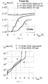
- Figure 5 N it comparison for Si passivated and NH 3 anneal passivated Ge n- and p-FETs.
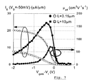
- Figure 7 Low field effective mobility ⁇ eff and corresponding I S -V G characteristics of 10 ⁇ m and 0.15 ⁇ m p-FETs.
- Figure 8 SRP current-voltage profile with and without silicon passivation layer.
- a method for making a passivated semiconductor substrate comprising the steps of providing a substrate surface comprising or consisting of a mono-crystalline semiconductor material other than silicon and forming a silicon layer on the substrate surface, such that the formed silicon layer is substantially lattice matched to at least part of the substrate surface (in particular is (substantially) lattice matched to said mono-crystalline semiconductor material).
- the mono-crystalline semiconductor material can comprise or can consist of any semiconductor material other than Si, more particularly can comprise or consist of Ge, GaAs, or any combination thereof.
- the silicon layer constitutes passivation of said part of the substrate surface (of said mono-crystalline semiconductor material) in relation to subsequent IC processing.
- passivation can be defined as making semiconductor material other than silicon chemically and electrically stable in relation to subsequent IC processing by reaction with silicon.
- the thickness of the formed silicon layer can be selected such that during and after at least one subsequent IC processing step the silicon layer constitutes passivation of said part of the substrate surface in relation to further IC processing.
- the thickness can be 1 to 6 monolayers, 1 to 4 monolayers, 1 to 2 monolayers, or 1 monolayer. However, in certain embodiments the thickness can be higher. In case of Ge devices, after gate oxide formation 1 monolayer could be enough to avoid contact between Ge and the gate oxide and have minimal influence on the Equivalent Oxide Thickness (EOT).
- EOT Equivalent Oxide Thickness
- the required silicon layer thickness can also be obtainable by providing a thicker layer than required, followed by oxidizing the silicon, or any other technique to decrease the silicon layer thickness, leaving the required number of monolayers of silicon.
- the required thickness can also be provided directly by a dedicated deposition process.
- Forming the silicon layer substantially lattice matched to the substrate surface can be done in different ways.
- One way can be epitaxial growth of silicon.
- Another possibility can be providing a non-epitaxial layer, followed by re-crystallization of the layer in order to make it lattice matched to the substrate surface.
- the silicon layer could be provided by different chemical vapor deposition techniques using a silicon precursor e.g. silane, dichlorosilane, trisilane or the like.
- a silicon precursor e.g. silane, dichlorosilane, trisilane or the like.
- epitaxial growth could be used, because this technique is able to form the silicon layer directly substantially lattice matched to the substrate surface.
- the silicon precursor could be silane, dichlorosilane, trisilane or the like, or a combination thereof.
- a carrier gas H 2 or preferably N 2 could be used.
- the deposition temperature can be 300 to 600°C depending on the silicon precursor and pressure can be between 10 torr (13.3 mbar) and 100 torr (133.3 mbar).
- the silicon layer is formed with trisilane and N 2 as carrier gas at 300°C.
- Rendering the semiconductor substrate surface substantially oxide free before forming the silicon layer could be done by subjecting the semiconductor surface to a solution containing HF, HBr, HI or any combination thereof, optionally followed by an annealing step in hydrogen ambient.
- An additional advantage of the invention is that, in case of fabricating devices on semiconductor substrates other than silicon, the process flow can be simplified by changing it partially into IC processing on silicon.
- a gate stack is deposited on top of the Ge channel.
- the Ge surface is passivated by forming a substantially lattice matched monolayer of silicon on top of it. This is done by growing a few monolayers of mono-crystalline silicon in an epireactor, e.g. ASM epsilon, at a temperature between 500 and 575°C, with 20 to 50sccm silane, a pressure of 40 torr (53.3 mbar) and 10 to 40slm N 2 as carrier gas. This mono-crystalline silicon layer is formed substantially lattice matched to the Ge.
- an epireactor e.g. ASM epsilon
- the Ge surface is subjected to a 1% HF solution, followed by anneal in H 2 ambient inside the chamber of the epireactor at a temperature between 650 and 850°C.
- the gate oxide is fabricated. This is done by oxidizing the silicon layer thermally, thereby leaving 1 to 2 monolayers of silicon between the Ge and the gate oxide, followed by depositing High-k material.
- Figure 1 shows a TEM picture of the resulting structure.
- Figure 2 describes such structure schematically.
- Figure 3 shows a C-V measurement of a p-type Ge capacitor fabricated in 3 different ways.
- the C-V curve shows a much more pronounced slope compared to the cases where this silicon layer is not present. This indicates that, in case of the presence of the silicon layer, the interface states density (N it ) at the Ge/gate oxide interface is decreased.
- Figure 4 shows the I-V curve of a p-type Ge capacitor fabricated with and without epitaxial silicon layer. In case the silicon layer is present, the breakdown voltage increases approximately 1 Volt.
- Table 1 comparison of the low field mobility ⁇ eff and the EOT between silicon passivated devices and relevant publications for p- and n-FETs.
- This invention relates to method for passivation of a semiconductor substrate other than silicon.
- It also relates to a semiconductor device comprising a passivated semiconductor substrate other than silicon and to a method to fabricate this device.
- Germanium (Ge) wafers are important substrates with technological applications in optical devices and are recently introduced as a replacement for Si substrates for advanced Integrated Circuit (IC) devices.
- Ge has very attractive advantages such as high mobility and compatibility with high-k and III/V materials.
- Galliumarsenide is another example of semiconductor materials, so-called III/V materials. These are often used in optical devices such as LED's, sensors, etc.
- Wu et al. teach a method for passivating a Ge layer, where an amorphous interfacial layer is deposited in SiH 4 ambient.
- Luan et al. teach a method of oxidation of Si on Ge, where a 35nm polycrystalline Si layer was deposited and then oxidized by exposure to dry oxygen gas.
- the invention provides a method for making a passivated semiconductor substrate comprising the steps of
- the semiconductor substrate can comprise Ge, GaAs, any other semiconductor material other than silicon, or any combination thereof.
- the silicon layer has a preferable thickness of 1 to 4 monolayers. However, in certain embodiments the thickness can be higher.
- the silicon layer has a thickness of 1 monolayer.
- a method according to the first aspect of the invention can further comprise the step of rendering the semiconductor substrate substantially free of oxides before the step of forming the silicon layer.
- the silicon layer is formed by epitaxial growth.
- the step of forming the silicon layer comprises exposure of the semiconductor substrate to silane.
- the step of forming the silicon layer comprises exposure of the semiconductor substrate to silane and to N 2 as carrier gas.
- the invention provides a semiconductor substrate other than silicon, passivated according to the first aspect of the invention.
- the passivated substrate is suitable to be measured by Spreading Resistance analysis techniques.
- the invention provides a semiconductor device comprising a passivated semiconductor substrate according to the first aspect of the invention.
- the invention provides a method for making a transistor comprising the step of providing a passivated semiconductor substrate according to the method provided in the first aspect of the invention.
- a method for making a passivated semiconductor substrate comprising the steps of providing a semiconductor substrate other than silicon and forming a silicon layer on the semiconductor substrate surface, characterized in that the silicon layer is formed substantially lattice matched to the substrate surface.
- the semiconductor substrate can comprise Ge, GaAs, any other semiconductor material other the Si, or any combination thereof.
- the thickness of the formed substantially lattice matched silicon layer can be preferably 1 to 4 monolayers, most preferably 1. 1 monolayer should be enough to avoid contact between Ge and the gate oxide and have minimal influence on the Equivalent Oxide Thickness (EOT).
- EOT Equivalent Oxide Thickness
- the required thickness can be obtained by providing a thicker layer than required, followed by oxidizing the silicon, or any other technique to decrease the silicon layer thickness, leaving the required number of monolayers of silicon.
- the required thickness can also be provided directly.
- Forming the silicon layer substantially lattice matched to the substrate surface can be done in different ways.
- One way is epitaxial growth of silicon.
- Another possibility is providing a non-epitaxial layer, followed by re-crystallization of the layer in order to make it lattice matched to the substrate surface.
- the silicon layer can be provided by different chemical vapor deposition techniques using a silicon precursor e.g. silane, dichlorosilane or the like.
- a silicon precursor e.g. silane, dichlorosilane or the like.
- epitaxial growth can be used, because this technique is able to form the silicon layer directly substantially lattice matched to the substrate surface.
- the silicon precursor can be silane, dichlorosilane, or the like, or a combination thereof.
- As a carrier gas H 2 or preferable N 2 can be used.
- the deposition temperature can be 500 to 600°C and pressure between 10 and 100 torr.
- Rendering the semiconductor substrate surface substantially oxide free before forming the silicon layer can be done by subjecting the semiconductor surface to a solution containing HF, HBr, HI or any combination thereof, optionally followed by an annealing step in hydrogen ambient.
- An additional advantage of the invention is that, in case of fabricating devices on semiconductor substrates other than silicon, the process flow can be simplified by changing it partially into IC processing on silicon.
- a gate stack is deposited on top of the Ge channel.
- the Ge surface is passivated by forming a substantially lattice matched monolayer of silicon on top of it. This is done by growing a few monolayers of mono-crystalline silicon in an epireactor, e.g. ASM epsilon, at a temperature between 575°C, with 20 to 50sccm silane, a pressure of 40 torr and 10 to 40slm N 2 as carrier gas. This mono-crystalline silicon layer is formed substantially lattice matched to the Ge.
- an epireactor e.g. ASM epsilon
- the Ge surface is subjected to a 1% HF solution , followed by an anneal in H 2 ambient inside the chamber of the epireactor at a temperature between 650 and 850°C.
- the gate oxide is fabricated. This is done by oxidizing the silicon layer thermally, thereby leaving one monolayer of silicon between the Ge and the gate oxide, followed by depositing High-k material.
- Figure 1 shows a TEM picture of the resulting structure.
- Figure 2 shows a CV measurement of a p-type Ge capacitor fabricated in 3 different ways. In case an epitaxial silicon layer is present between the Ge and the gate oxide, the CV curve shows a much more pronounced slope compared to the cases where this silicon layer is not present. This indicates that, in case of the presence of the silicon layer, the interface states density at the Ge/gate oxide interface is decreased.
- Figure 3 shows the IV curve of a p-type Ge capacitor fabricated with and without epitaxial silicon layer. In case the silicon layer is present, the breakdown voltage increases approximately 1 Volt.
Landscapes
- Insulated Gate Type Field-Effect Transistor (AREA)
- Formation Of Insulating Films (AREA)
- Metal-Oxide And Bipolar Metal-Oxide Semiconductor Integrated Circuits (AREA)
- Recrystallisation Techniques (AREA)
- Semiconductor Integrated Circuits (AREA)
- Crystals, And After-Treatments Of Crystals (AREA)
Abstract
- providing a mono-crystalline substrate surface comprising or consisting of semiconductor material other than silicon and
- forming a silicon layer on the substrate surface, such that the formed silicon layer is substantially lattice matched to said part of the substrate surface.
Description
- This invention relates to method for passivation of a semiconductor substrate comprising semiconductor material other than silicon.
- It also relates to a semiconductor device comprising such passivated semiconductor substrate.
- In microelectronics industry, a lot of different semiconductor materials are used besides Silicon (Si). For example Germanium (Ge) wafers are important substrates with technological applications in optical devices and are recently introduced as a replacement for Si substrates for advanced Integrated Circuit (IC) devices. Ge has very attractive advantages such as high mobility and compatibility with high-k and III/V materials.
- Galliumarsenide (GaAs) is another example of semiconductor materials, so-called III/V materials. These are often used in optical devices such as LED's, sensors, etc.
- When processing wafers containing these alternative materials, dedicated process conditions have to be developed.
- Especially in case of deposition of gate stacks on Ge, one has to deal with a lot of difficulties and challenges. One of the major problems here is the high interface states density (Nit) at the interface between Ge substrate and gate dielectric, causing bad capacitance-voltage (C-V curve) and current density-voltage (I-V curve) device characteristics.
- Also for analysis of mentioned alternative semiconductor materials, especially in case of Spreading Resistance measurements, the problem of high interface states density influences the measurement.
- A few attempts to decrease the problem of high interface states density between Ge substrate and gate oxide are known in prior art.
- In "A TaN-HfO2-Ge pMOSFET with novel SiH4 surface passivation", Wu et al. teach a method for passivating a Ge layer, wherein an amorphous interfacial layer is deposited in SiH4 ambient.
- In US 6,352,942 Luan et al. teach a method of oxidation of Si on Ge, wherein a 35nm polycrystalline Si layer was deposited and then oxidized by exposure to dry oxygen gas.
- The present invention aims to provide a method for passivating a semiconductor substrate comprising semiconductor material other than silicon in relation to further IC processing.
- The present invention relates to a method for passivating a semiconductor substrate comprising the steps of:
- providing a substrate surface comprising (or consisting of) a mono-crystalline semiconductor material, said material being different from silicon, and
- forming a silicon layer on the substrate surface, such that said silicon layer is (substantially) lattice matched to said mono-crystalline semiconductor material.
- The mono-crystalline semiconductor material can comprise or can consist of any semiconductor material other than silicon, more particularly can comprise or consist of Ge, GaAs, or any combination thereof.
- In a method according to the present invention, the silicon layer constitutes passivation of said part of the substrate surface (of said mono-crystalline semiconductor material) in relation to subsequent IC processing.
- In a method according to the present invention, the thickness of the formed silicon layer can be selected such that during and after at least one subsequent IC processing step the silicon layer constitutes passivation of said part of the substrate surface (of said mono-crystalline semiconductor material) in relation to further IC processing.
- After said at least one subsequent IC processing step, the thickness can be 1 to 6 monolayers, 1 to 4 monolayers, 1 to 2 monolayers, or even 1 monolayer. However, in certain embodiments the thickness can be higher.
- Subsequent IC processing can comprise a processing step such as but not limited to oxidation of a part of the silicon layer, formation of a dielectric layer stack, or formation of a gate stack.
- A method according to the present invention can further comprise the step of rendering the relevant part of the semiconductor substrate, in particular the mono-crystalline semiconductor material, substantially free of oxides before the step of forming the silicon layer.
- In a method according to the present invention, the silicon layer can be formed by epitaxial growth.
- Silane, dichlorosilane, trisilane, or the like, or a combination thereof can be used as silicon precursor(s).
- H2 can be used as carrier gas. Preferably N2 can be used as carrier gas.
- In a preferred method the silicon layer is formed with trisilane as silicon precursor and N2 as carrier gas.
- The present invention provides further a passivated semiconductor substrate according to a method of the present invention.
- This passivated semiconductor substrate can be used in a semiconductor device.
- This passivated substrate surface can also be suitable to be measured by Spreading Resistance analysis techniques.
- Figure 1: TEM picture of a high-k gate stack on Ge passivated with silicon.
- Figure 2: Schematic description of a high-k gate stack on Ge passivated with silicon.
- Figure 3: C-V measurement of a p-type Ge capacitor fabricated in 3 different ways.
- Figure 4: I-V curve of a p-type Ge capacitor fabricated with and without epitaxial silicon layer.
- Figure 5: Nit comparison for Si passivated and NH3 anneal passivated Ge n- and p-FETs.
- Figure 6: Low field effective mobility µeff and corresponding IS-VG characteristics of 10µm and 0.15µm n-FETs.
- Figure 7: Low field effective mobility µeff and corresponding IS-VG characteristics of 10µm and 0.15µm p-FETs.
- Figure 8: SRP current-voltage profile with and without silicon passivation layer.
- To solve the problem of high interface states density, a method for making a passivated semiconductor substrate is disclosed comprising the steps of providing a substrate surface comprising or consisting of a mono-crystalline semiconductor material other than silicon and forming a silicon layer on the substrate surface, such that the formed silicon layer is substantially lattice matched to at least part of the substrate surface (in particular is (substantially) lattice matched to said mono-crystalline semiconductor material).
- The mono-crystalline semiconductor material can comprise or can consist of any semiconductor material other than Si, more particularly can comprise or consist of Ge, GaAs, or any combination thereof.
- In a method according to the present invention, the silicon layer constitutes passivation of said part of the substrate surface (of said mono-crystalline semiconductor material) in relation to subsequent IC processing.
- In the context of the present invention, passivation can be defined as making semiconductor material other than silicon chemically and electrically stable in relation to subsequent IC processing by reaction with silicon.
- In a method according to the present invention, the thickness of the formed silicon layer can be selected such that during and after at least one subsequent IC processing step the silicon layer constitutes passivation of said part of the substrate surface in relation to further IC processing.
- After said at least one subsequent IC processing step, the thickness can be 1 to 6 monolayers, 1 to 4 monolayers, 1 to 2 monolayers, or 1 monolayer. However, in certain embodiments the thickness can be higher. In case of Ge devices, after
gate oxide formation 1 monolayer could be enough to avoid contact between Ge and the gate oxide and have minimal influence on the Equivalent Oxide Thickness (EOT). - The required silicon layer thickness can also be obtainable by providing a thicker layer than required, followed by oxidizing the silicon, or any other technique to decrease the silicon layer thickness, leaving the required number of monolayers of silicon. The required thickness can also be provided directly by a dedicated deposition process.
- Forming the silicon layer substantially lattice matched to the substrate surface (in particular to the mono-crystalline semiconductor material) can be done in different ways.
- One way can be epitaxial growth of silicon.
- Another possibility can be providing a non-epitaxial layer, followed by re-crystallization of the layer in order to make it lattice matched to the substrate surface.
- The silicon layer could be provided by different chemical vapor deposition techniques using a silicon precursor e.g. silane, dichlorosilane, trisilane or the like. Preferably, epitaxial growth could be used, because this technique is able to form the silicon layer directly substantially lattice matched to the substrate surface.
- In case of LPCVD epitaxial growth, the silicon precursor could be silane, dichlorosilane, trisilane or the like, or a combination thereof. As a carrier gas, H2 or preferably N2 could be used. The deposition temperature can be 300 to 600°C depending on the silicon precursor and pressure can be between 10 torr (13.3 mbar) and 100 torr (133.3 mbar). In a preferred method the silicon layer is formed with trisilane and N2 as carrier gas at 300°C.
- Rendering the semiconductor substrate surface substantially oxide free before forming the silicon layer could be done by subjecting the semiconductor surface to a solution containing HF, HBr, HI or any combination thereof, optionally followed by an annealing step in hydrogen ambient.
- An additional advantage of the invention is that, in case of fabricating devices on semiconductor substrates other than silicon, the process flow can be simplified by changing it partially into IC processing on silicon.
- In order to make a Ge capacitor, a gate stack is deposited on top of the Ge channel. To avoid a high interface state density at the interface between the Ge channel and the gate oxide, the Ge surface is passivated by forming a substantially lattice matched monolayer of silicon on top of it. This is done by growing a few monolayers of mono-crystalline silicon in an epireactor, e.g. ASM epsilon, at a temperature between 500 and 575°C, with 20 to 50sccm silane, a pressure of 40 torr (53.3 mbar) and 10 to 40slm N2 as carrier gas. This mono-crystalline silicon layer is formed substantially lattice matched to the Ge.
- In order to be able to grow epitaxially on the Ge surface and to remove substantially all germanium oxide on top of it, a surface preparation is done. Therefore, the Ge surface is subjected to a 1% HF solution, followed by anneal in H2 ambient inside the chamber of the epireactor at a temperature between 650 and 850°C.
- After the mono-crystalline growth of 4 to 5 monolayers of silicon, the gate oxide is fabricated. This is done by oxidizing the silicon layer thermally, thereby leaving 1 to 2 monolayers of silicon between the Ge and the gate oxide, followed by depositing High-k material. Figure 1 shows a TEM picture of the resulting structure. Figure 2 describes such structure schematically.
- Figure 3 shows a C-V measurement of a p-type Ge capacitor fabricated in 3 different ways. In case an epitaxial silicon layer is present between the Ge and the gate oxide, the C-V curve shows a much more pronounced slope compared to the cases where this silicon layer is not present. This indicates that, in case of the presence of the silicon layer, the interface states density (Nit) at the Ge/gate oxide interface is decreased. Figure 4 shows the I-V curve of a p-type Ge capacitor fabricated with and without epitaxial silicon layer. In case the silicon layer is present, the breakdown voltage increases approximately 1 Volt.
- Also 10µm*10µm Ge n- and p-FET devices with four monolayers of silicon are fabricated. Charge pumping measurements on these devices confirm the reduced amount of Nit as compared to an NH3 anneal passivation treatment, which is a commonly used technique. In figure 5 is shown that the reduction is about one decade, yielding values of 5e11cm-2 for p-FET and 1.5e12cm-2 for n-FET.
- As a consequence of the lower Nit, device lots with Si passivation yield promising deep-sub micron n- and p-FET devices. Their low field effective mobility µeff and corresponding IS-VG characteristics are shown in fig. 6 and 7. The p-FET mobility obtained in silicon passivated conventional 10µm and 0.15µm devices is in line with the values obtained with NH3 or PH3 passivation on ring-shaped long channel devices (table 1). The n-FET mobility is still low, although significantly superior to the data published for NH3 passivation. Good n-FET mobility has only been reported for the PH3 passivation.
- Table 1: comparison of the low field mobility µeff and the EOT between silicon passivated devices and relevant publications for p- and n-FETs.
p-FET n-FET µeff(cm2/Vs) EOT (Å) µeff(cm2/Vs) EOT (Å) Si passivated 170 26 10 26 NH3 210 16 ~0.2 ? PH3 125 17? 300 17? - In case of Spreading Resistance analysis, e.g. SRP (Spreading Resistance Probing) and SSRM (Scanning Spreading Resistance Microscopy), on doped Ge substrates, point contacts are realized between the metal probe and the Ge surface. When contacting the Ge directly with the probe, a Shottky contact is created due to generation of a depletion layer at the Ge side. When passivating the doped Ge substrate with a mono-crystalline undoped silicon layer as claimed in the present invention, the Shottky contact is modified into a substantially Ohmic contact. Figure 8 proofs that doped Ge samples with an epitaxially grown mono-crystalline silicon layer of two monolayers thickness show an approximately Ohmic current-voltage profile compared to the samples without silicon layer. This simplifies Spreading Resistance analysis and improves it's accuracy to a high extend.
- The following paragraphs constitute another way of describing the invention, and correspond to the description made in the priority document.
- This invention relates to method for passivation of a semiconductor substrate other than silicon.
- It also relates to a semiconductor device comprising a passivated semiconductor substrate other than silicon and to a method to fabricate this device.
- In microelectronics industry, a lot of different semiconductor materials are used besides Silicon (Si). For example Germanium (Ge) wafers are important substrates with technological applications in optical devices and are recently introduced as a replacement for Si substrates for advanced Integrated Circuit (IC) devices. Ge has very attractive advantages such as high mobility and compatibility with high-k and III/V materials.
- Galliumarsenide (GaAs) is another example of semiconductor materials, so-called III/V materials. These are often used in optical devices such as LED's, sensors, etc.
- When processing wafers containing these alternative materials, dedicated process conditions have to be developed. Especially in case of deposition of gate stacks on Ge, one has to deal with a lot of difficulties and challenges.
- One of the major problems is the high interface states density at the interface between Ge substrate and gate oxide, causing bad capacitance-voltage (CV) and current density-voltage (IV) device characteristics.
- Also for analysis of mentioned alternative semiconductor materials, especially in case of Spreading Resistance measurements, the problem of high interface states density influences the measurement.
- A few attempts to decrease the problem of high interface states density between Ge substrate and gate oxide are known in prior art.
- In "A TaN-HfO2-Ge pMOSFET with novel SiH4 surface passivation", Wu et al. teach a method for passivating a Ge layer, where an amorphous interfacial layer is deposited in SiH4 ambient.
- In US 6,352,942 Luan et al. teach a method of oxidation of Si on Ge, where a 35nm polycrystalline Si layer was deposited and then oxidized by exposure to dry oxygen gas.
- In a first aspect the invention provides a method for making a passivated semiconductor substrate comprising the steps of
- providing a semiconductor substrate other than silicon and
- forming a silicon layer on the substrate surface,
- The semiconductor substrate can comprise Ge, GaAs, any other semiconductor material other than silicon, or any combination thereof.
- In a method according to the first aspect of the invention, the silicon layer has a preferable thickness of 1 to 4 monolayers. However, in certain embodiments the thickness can be higher.
- In a method according to the first aspect of the invention, the silicon layer has a thickness of 1 monolayer.
- A method according to the first aspect of the invention can further comprise the step of rendering the semiconductor substrate substantially free of oxides before the step of forming the silicon layer.
- In a method according to the first aspect of the invention, the silicon layer is formed by epitaxial growth.
- In a method according to the first aspect of the invention, the step of forming the silicon layer comprises exposure of the semiconductor substrate to silane.
- In a method according to the first aspect of the invention, the step of forming the silicon layer comprises exposure of the semiconductor substrate to silane and to N2 as carrier gas.
- In a second aspect the invention provides a semiconductor substrate other than silicon, passivated according to the first aspect of the invention.
- In a method according to the second aspect of the invention, the passivated substrate is suitable to be measured by Spreading Resistance analysis techniques.
- In a third aspect the invention provides a semiconductor device comprising a passivated semiconductor substrate according to the first aspect of the invention.
- In a fourth aspect the invention provides a method for making a transistor comprising the step of providing a passivated semiconductor substrate according to the method provided in the first aspect of the invention.
- To solve the problem of high interface states density, a method for making a passivated semiconductor substrate is disclosed comprising the steps of providing a semiconductor substrate other than silicon and forming a silicon layer on the semiconductor substrate surface, characterized in that the silicon layer is formed substantially lattice matched to the substrate surface.
- The semiconductor substrate can comprise Ge, GaAs, any other semiconductor material other the Si, or any combination thereof.
- The thickness of the formed substantially lattice matched silicon layer can be preferably 1 to 4 monolayers, most preferably 1. 1 monolayer should be enough to avoid contact between Ge and the gate oxide and have minimal influence on the Equivalent Oxide Thickness (EOT).
- The required thickness can be obtained by providing a thicker layer than required, followed by oxidizing the silicon, or any other technique to decrease the silicon layer thickness, leaving the required number of monolayers of silicon. The required thickness can also be provided directly.
- Forming the silicon layer substantially lattice matched to the substrate surface can be done in different ways. One way is epitaxial growth of silicon. Another possibility is providing a non-epitaxial layer, followed by re-crystallization of the layer in order to make it lattice matched to the substrate surface.
- The silicon layer can be provided by different chemical vapor deposition techniques using a silicon precursor e.g. silane, dichlorosilane or the like. Preferably, epitaxial growth can be used, because this technique is able to form the silicon layer directly substantially lattice matched to the substrate surface. In case of LPCVD epitaxial growth, the silicon precursor can be silane, dichlorosilane, or the like, or a combination thereof. As a carrier gas, H2 or preferable N2 can be used. The deposition temperature can be 500 to 600°C and pressure between 10 and 100 torr.
- Rendering the semiconductor substrate surface substantially oxide free before forming the silicon layer can be done by subjecting the semiconductor surface to a solution containing HF, HBr, HI or any combination thereof, optionally followed by an annealing step in hydrogen ambient.
- An additional advantage of the invention is that, in case of fabricating devices on semiconductor substrates other than silicon, the process flow can be simplified by changing it partially into IC processing on silicon.
- In order to make a Ge capacitor, a gate stack is deposited on top of the Ge channel. To avoid a high interface state density at the interface between the Ge channel and the gate oxide, the Ge surface is passivated by forming a substantially lattice matched monolayer of silicon on top of it. This is done by growing a few monolayers of mono-crystalline silicon in an epireactor, e.g. ASM epsilon, at a temperature between 575°C, with 20 to 50sccm silane, a pressure of 40 torr and 10 to 40slm N2 as carrier gas. This mono-crystalline silicon layer is formed substantially lattice matched to the Ge.
- In order to be able to grow epitaxially on the Ge surface and to remove substantially all germanium oxide on top of it, a surface preparation is done. Therefore, the Ge surface is subjected to a 1% HF solution , followed by an anneal in H2 ambient inside the chamber of the epireactor at a temperature between 650 and 850°C.
- After the mono-crystalline growth of 3 monolayers of silicon, the gate oxide is fabricated. This is done by oxidizing the silicon layer thermally, thereby leaving one monolayer of silicon between the Ge and the gate oxide, followed by depositing High-k material. Figure 1 shows a TEM picture of the resulting structure. Figure 2 shows a CV measurement of a p-type Ge capacitor fabricated in 3 different ways. In case an epitaxial silicon layer is present between the Ge and the gate oxide, the CV curve shows a much more pronounced slope compared to the cases where this silicon layer is not present. This indicates that, in case of the presence of the silicon layer, the interface states density at the Ge/gate oxide interface is decreased. Figure 3 shows the IV curve of a p-type Ge capacitor fabricated with and without epitaxial silicon layer. In case the silicon layer is present, the breakdown voltage increases approximately 1 Volt.
- In case of Spreading Resistance analysis, e.g. SRP and SSRM, on doped Ge substrates, point contacts are realized between the metal probe and the Ge surface. When contacting the Ge directly with the probe, a Shottky contact is created due to generation of a depletion layer at the Ge side. When passivating the doped Ge substrate with a mono-crystalline undoped silicon layer, the Shottky contact is modified into a substantially Ohmic contact. Figure 4 proofs that doped Ge samples with an epitaxially grown mono-crystalline silicon layer of two monolayers thickness show an approximately Ohmic current-voltage profile compared to the samples without silicon layer. This simplifies Spreading Resistance analysis and improves it's accuracy to a high extend.
Claims (14)
- A method for passivating a semiconductor substrate comprising the steps of:- providing a substrate surface comprising a mono-crystalline semiconductor material which is not silicon, and- forming a substantially lattice matched silicon layer on said mono-crystalline semiconductor material.
- A method according to claim 1, wherein said mono-crystalline semiconductor material is Ge, GaAs, or any combination thereof.
- A method according to claim 1 or 2, wherein said silicon layer acts as a passivating layer in subsequent IC processing.
- A method according to any of claims 1 to 3, wherein the thickness of said silicon layer is such that during and after at least one subsequent IC processing step the remaining silicon layer still acts as a passivating layer.
- A method according to claim 4, wherein after said at least one subsequent IC processing step the silicon layer thickness is 1 to 6 monolayers, 1 to 4 monolayers, 1 to 2 monolayers, or 1 monolayer.
- A method according to any of claims 1 to 5, further comprising the step of rendering said mono-crystalline semiconductor material substantially free of oxides before the step of forming the silicon layer.
- A method according to any of claims 1 to 6, further comprising the steps of:- oxidating at least a part of said silicon layer, and/or- forming a dielectric layer stack, and/or- forming a gate stack.
- A method according to any of claims 1 to 7, wherein said silicon layer is formed by epitaxial growth.
- A method according to claim 8, wherein silane, dichlorosilane, trisilane or the like, or a combination thereof is/are used as silicon precursor(s).
- A method according to claim 9, wherein N2 is used as carrier gas.
- A method according to claim 10, wherein trisilane is used as silicon precursor and N2 is used as carrier gas.
- A passivated semiconductor substrate obtainable by a method according to any of claims 1 to 11.
- A passivated semiconductor substrate according to claim 12, having an Omhic current-voltage profile which can be measured by Spreading Resistance analysis techniques.
- Use of the passivated semiconductor substrate according to claim 12 or 13 in a semiconductor device.
Applications Claiming Priority (1)
| Application Number | Priority Date | Filing Date | Title |
|---|---|---|---|
| US61886304P | 2004-10-13 | 2004-10-13 |
Publications (3)
| Publication Number | Publication Date |
|---|---|
| EP1655767A2 true EP1655767A2 (en) | 2006-05-10 |
| EP1655767A3 EP1655767A3 (en) | 2006-06-21 |
| EP1655767B1 EP1655767B1 (en) | 2017-03-22 |
Family
ID=36168907
Family Applications (1)
| Application Number | Title | Priority Date | Filing Date |
|---|---|---|---|
| EP05447233.7A Expired - Lifetime EP1655767B1 (en) | 2004-10-13 | 2005-10-13 | Method for making a passivated semiconductor substrate |
Country Status (3)
| Country | Link |
|---|---|
| US (1) | US20060086950A1 (en) |
| EP (1) | EP1655767B1 (en) |
| JP (1) | JP5047486B2 (en) |
Cited By (1)
| Publication number | Priority date | Publication date | Assignee | Title |
|---|---|---|---|---|
| DE112011103249B4 (en) * | 2010-09-28 | 2014-01-23 | International Business Machines Corporation | A gate-stack semiconductor device and a method of manufacturing the same, and the use of a gate-stack structure in a semiconductor device |
Families Citing this family (4)
| Publication number | Priority date | Publication date | Assignee | Title |
|---|---|---|---|---|
| WO2007138063A1 (en) * | 2006-05-26 | 2007-12-06 | Interuniversitair Microelektronica Centrum (Imec) | Method for reducing the surface roughness of a semiconductor substrate |
| GB0802088D0 (en) * | 2008-02-05 | 2008-03-12 | Panalytical Bv | Imaging detector |
| EP2461352B1 (en) | 2010-12-06 | 2013-07-10 | Imec | Method of manufacturing low resistivity contacts on n-type germanium |
| US8809152B2 (en) * | 2011-11-18 | 2014-08-19 | International Business Machines Corporation | Germanium oxide free atomic layer deposition of silicon oxide and high-k gate dielectric on germanium containing channel for CMOS devices |
Citations (1)
| Publication number | Priority date | Publication date | Assignee | Title |
|---|---|---|---|---|
| US6352942B1 (en) | 1999-06-25 | 2002-03-05 | Massachusetts Institute Of Technology | Oxidation of silicon on germanium |
Family Cites Families (9)
| Publication number | Priority date | Publication date | Assignee | Title |
|---|---|---|---|---|
| JPS57211238A (en) * | 1981-06-22 | 1982-12-25 | Nec Corp | Semiconductor device |
| JPS63252478A (en) * | 1987-04-09 | 1988-10-19 | Seiko Instr & Electronics Ltd | Insulated-gate semiconductor device |
| US4987095A (en) * | 1988-06-15 | 1991-01-22 | International Business Machines Corp. | Method of making unpinned oxide-compound semiconductor structures |
| JPH03116834A (en) * | 1989-09-29 | 1991-05-17 | Nec Corp | Manufacture of semiconductor structure using n-type gaas |
| US5168330A (en) * | 1990-12-03 | 1992-12-01 | Research Triangle Institute | Semiconductor device having a semiconductor substrate interfaced to a dissimilar material by means of a single crystal pseudomorphic interlayer |
| JP3147036B2 (en) * | 1997-05-02 | 2001-03-19 | 日本電気株式会社 | Compound semiconductor device and method of manufacturing the same |
| US6607948B1 (en) * | 1998-12-24 | 2003-08-19 | Kabushiki Kaisha Toshiba | Method of manufacturing a substrate using an SiGe layer |
| AU2002306436A1 (en) * | 2001-02-12 | 2002-10-15 | Asm America, Inc. | Improved process for deposition of semiconductor films |
| US7026219B2 (en) * | 2001-02-12 | 2006-04-11 | Asm America, Inc. | Integration of high k gate dielectric |
-
2005
- 2005-10-13 US US11/249,642 patent/US20060086950A1/en not_active Abandoned
- 2005-10-13 EP EP05447233.7A patent/EP1655767B1/en not_active Expired - Lifetime
- 2005-10-13 JP JP2005299280A patent/JP5047486B2/en not_active Expired - Lifetime
Patent Citations (1)
| Publication number | Priority date | Publication date | Assignee | Title |
|---|---|---|---|---|
| US6352942B1 (en) | 1999-06-25 | 2002-03-05 | Massachusetts Institute Of Technology | Oxidation of silicon on germanium |
Cited By (1)
| Publication number | Priority date | Publication date | Assignee | Title |
|---|---|---|---|---|
| DE112011103249B4 (en) * | 2010-09-28 | 2014-01-23 | International Business Machines Corporation | A gate-stack semiconductor device and a method of manufacturing the same, and the use of a gate-stack structure in a semiconductor device |
Also Published As
| Publication number | Publication date |
|---|---|
| EP1655767A3 (en) | 2006-06-21 |
| EP1655767B1 (en) | 2017-03-22 |
| JP5047486B2 (en) | 2012-10-10 |
| JP2006173574A (en) | 2006-06-29 |
| US20060086950A1 (en) | 2006-04-27 |
Similar Documents
| Publication | Publication Date | Title |
|---|---|---|
| US11456219B2 (en) | Gate-all-around FETs having uniform threshold voltage | |
| US7919381B2 (en) | Germanium substrate-type materials and approach therefor | |
| De Jaeger et al. | Optimisation of a thin epitaxial Si layer as Ge passivation layer to demonstrate deep sub-micron n-and p-FETs on Ge-On-Insulator substrates | |
| US6653700B2 (en) | Transistor structure and method of fabrication | |
| CN101454874B (en) | Selective epitaxial formation of semiconductor films | |
| US7355235B2 (en) | Semiconductor device and method for high-k gate dielectrics | |
| US9087927B2 (en) | Thermally stable high-K tetragonal HFO2 layer within high aspect ratio deep trenches | |
| US6323143B1 (en) | Method for making silicon nitride-oxide ultra-thin gate insulating layers for submicrometer field effect transistors | |
| US20030193061A1 (en) | Electronic component and method for producing an electronic component | |
| US6974738B2 (en) | Nonplanar device with stress incorporation layer and method of fabrication | |
| US20030155582A1 (en) | Gate dielectric structures for integrated circuits and methods for making and using such gate dielectric structures | |
| KR100843866B1 (en) | FIELD-EFFECT TRANSISTOR INCLUDING SPLIT POLY-SiGe/POLY-Si ALLOY GATE STACK AND SEMICONDUCTOR DEVICE INCLUDING THEREOF | |
| EP1872409A1 (en) | Ultra-thin hf-doped silicon oxynitride film for high performance cmos applications and method of manufacture | |
| US20060094192A1 (en) | Method for treating base oxide to improve high-K material deposition | |
| US20130264658A1 (en) | Reduced S/D Contact Resistance of III-V Mosfet Using Low Temperature Metal-Induced Crystallilzation of n+ Ge | |
| US8361889B2 (en) | Strained semiconductor-on-insulator by addition and removal of atoms in a semiconductor-on-insulator | |
| US20080153266A1 (en) | Method to improve the selective epitaxial growth (seg) process | |
| EP1655767B1 (en) | Method for making a passivated semiconductor substrate | |
| US20030197231A1 (en) | Semiconductor device and method of manufacturing the same | |
| US20020020861A1 (en) | Semiconductor device and method of fabricating the same | |
| US20060088966A1 (en) | Semiconductor device having a smooth EPI layer and a method for its manufacture | |
| US20060166454A1 (en) | Low tolerance polysilicon resistor for low temperature silicide processing | |
| EP1936670A2 (en) | Method to improve the Selective Epitaxial Growth (SEG) Process | |
| US12512312B1 (en) | Vertical gallium nitride containing field effect transistor with silicon nitride passivation and gate dielectric regions | |
| Destefanis et al. | Fabrication, structural and electrical properties of (1 1 0) localized silicon-on-insulator devices |
Legal Events
| Date | Code | Title | Description |
|---|---|---|---|
| PUAI | Public reference made under article 153(3) epc to a published international application that has entered the european phase |
Free format text: ORIGINAL CODE: 0009012 |
|
| AK | Designated contracting states |
Kind code of ref document: A2 Designated state(s): AT BE BG CH CY CZ DE DK EE ES FI FR GB GR HU IE IS IT LI LT LU LV MC NL PL PT RO SE SI SK TR |
|
| AX | Request for extension of the european patent |
Extension state: AL BA HR MK YU |
|
| PUAL | Search report despatched |
Free format text: ORIGINAL CODE: 0009013 |
|
| AK | Designated contracting states |
Kind code of ref document: A3 Designated state(s): AT BE BG CH CY CZ DE DK EE ES FI FR GB GR HU IE IS IT LI LT LU LV MC NL PL PT RO SE SI SK TR |
|
| AX | Request for extension of the european patent |
Extension state: AL BA HR MK YU |
|
| 17P | Request for examination filed |
Effective date: 20061026 |
|
| 17Q | First examination report despatched |
Effective date: 20061214 |
|
| AKX | Designation fees paid |
Designated state(s): AT BE BG CH CY CZ DE DK EE ES FI FR GB GR HU IE IS IT LI LT LU LV MC NL PL PT RO SE SI SK TR |
|
| RAP1 | Party data changed (applicant data changed or rights of an application transferred) |
Owner name: IMEC |
|
| REG | Reference to a national code |
Ref country code: DE Ref legal event code: R079 Ref document number: 602005051561 Country of ref document: DE Free format text: PREVIOUS MAIN CLASS: H01L0021280000 Ipc: H01L0021020000 |
|
| GRAP | Despatch of communication of intention to grant a patent |
Free format text: ORIGINAL CODE: EPIDOSNIGR1 |
|
| RIC1 | Information provided on ipc code assigned before grant |
Ipc: H01L 21/316 20060101ALI20160921BHEP Ipc: H01L 21/02 20060101AFI20160921BHEP |
|
| INTG | Intention to grant announced |
Effective date: 20161007 |
|
| GRAS | Grant fee paid |
Free format text: ORIGINAL CODE: EPIDOSNIGR3 |
|
| GRAA | (expected) grant |
Free format text: ORIGINAL CODE: 0009210 |
|
| AK | Designated contracting states |
Kind code of ref document: B1 Designated state(s): AT BE BG CH CY CZ DE DK EE ES FI FR GB GR HU IE IS IT LI LT LU LV MC NL PL PT RO SE SI SK TR |
|
| REG | Reference to a national code |
Ref country code: GB Ref legal event code: FG4D |
|
| REG | Reference to a national code |
Ref country code: CH Ref legal event code: EP |
|
| REG | Reference to a national code |
Ref country code: AT Ref legal event code: REF Ref document number: 878526 Country of ref document: AT Kind code of ref document: T Effective date: 20170415 |
|
| REG | Reference to a national code |
Ref country code: IE Ref legal event code: FG4D |
|
| REG | Reference to a national code |
Ref country code: DE Ref legal event code: R096 Ref document number: 602005051561 Country of ref document: DE |
|
| REG | Reference to a national code |
Ref country code: NL Ref legal event code: MP Effective date: 20170322 |
|
| PG25 | Lapsed in a contracting state [announced via postgrant information from national office to epo] |
Ref country code: GR Free format text: LAPSE BECAUSE OF FAILURE TO SUBMIT A TRANSLATION OF THE DESCRIPTION OR TO PAY THE FEE WITHIN THE PRESCRIBED TIME-LIMIT Effective date: 20170623 Ref country code: FI Free format text: LAPSE BECAUSE OF FAILURE TO SUBMIT A TRANSLATION OF THE DESCRIPTION OR TO PAY THE FEE WITHIN THE PRESCRIBED TIME-LIMIT Effective date: 20170322 Ref country code: LT Free format text: LAPSE BECAUSE OF FAILURE TO SUBMIT A TRANSLATION OF THE DESCRIPTION OR TO PAY THE FEE WITHIN THE PRESCRIBED TIME-LIMIT Effective date: 20170322 |
|
| REG | Reference to a national code |
Ref country code: LT Ref legal event code: MG4D |
|
| REG | Reference to a national code |
Ref country code: AT Ref legal event code: MK05 Ref document number: 878526 Country of ref document: AT Kind code of ref document: T Effective date: 20170322 |
|
| PG25 | Lapsed in a contracting state [announced via postgrant information from national office to epo] |
Ref country code: SE Free format text: LAPSE BECAUSE OF FAILURE TO SUBMIT A TRANSLATION OF THE DESCRIPTION OR TO PAY THE FEE WITHIN THE PRESCRIBED TIME-LIMIT Effective date: 20170322 Ref country code: LV Free format text: LAPSE BECAUSE OF FAILURE TO SUBMIT A TRANSLATION OF THE DESCRIPTION OR TO PAY THE FEE WITHIN THE PRESCRIBED TIME-LIMIT Effective date: 20170322 Ref country code: BG Free format text: LAPSE BECAUSE OF FAILURE TO SUBMIT A TRANSLATION OF THE DESCRIPTION OR TO PAY THE FEE WITHIN THE PRESCRIBED TIME-LIMIT Effective date: 20170622 |
|
| REG | Reference to a national code |
Ref country code: FR Ref legal event code: PLFP Year of fee payment: 13 |
|
| PG25 | Lapsed in a contracting state [announced via postgrant information from national office to epo] |
Ref country code: NL Free format text: LAPSE BECAUSE OF FAILURE TO SUBMIT A TRANSLATION OF THE DESCRIPTION OR TO PAY THE FEE WITHIN THE PRESCRIBED TIME-LIMIT Effective date: 20170322 |
|
| PG25 | Lapsed in a contracting state [announced via postgrant information from national office to epo] |
Ref country code: IT Free format text: LAPSE BECAUSE OF FAILURE TO SUBMIT A TRANSLATION OF THE DESCRIPTION OR TO PAY THE FEE WITHIN THE PRESCRIBED TIME-LIMIT Effective date: 20170322 Ref country code: SK Free format text: LAPSE BECAUSE OF FAILURE TO SUBMIT A TRANSLATION OF THE DESCRIPTION OR TO PAY THE FEE WITHIN THE PRESCRIBED TIME-LIMIT Effective date: 20170322 Ref country code: CZ Free format text: LAPSE BECAUSE OF FAILURE TO SUBMIT A TRANSLATION OF THE DESCRIPTION OR TO PAY THE FEE WITHIN THE PRESCRIBED TIME-LIMIT Effective date: 20170322 Ref country code: EE Free format text: LAPSE BECAUSE OF FAILURE TO SUBMIT A TRANSLATION OF THE DESCRIPTION OR TO PAY THE FEE WITHIN THE PRESCRIBED TIME-LIMIT Effective date: 20170322 Ref country code: AT Free format text: LAPSE BECAUSE OF FAILURE TO SUBMIT A TRANSLATION OF THE DESCRIPTION OR TO PAY THE FEE WITHIN THE PRESCRIBED TIME-LIMIT Effective date: 20170322 Ref country code: RO Free format text: LAPSE BECAUSE OF FAILURE TO SUBMIT A TRANSLATION OF THE DESCRIPTION OR TO PAY THE FEE WITHIN THE PRESCRIBED TIME-LIMIT Effective date: 20170322 Ref country code: ES Free format text: LAPSE BECAUSE OF FAILURE TO SUBMIT A TRANSLATION OF THE DESCRIPTION OR TO PAY THE FEE WITHIN THE PRESCRIBED TIME-LIMIT Effective date: 20170322 |
|
| PG25 | Lapsed in a contracting state [announced via postgrant information from national office to epo] |
Ref country code: PL Free format text: LAPSE BECAUSE OF FAILURE TO SUBMIT A TRANSLATION OF THE DESCRIPTION OR TO PAY THE FEE WITHIN THE PRESCRIBED TIME-LIMIT Effective date: 20170322 Ref country code: IS Free format text: LAPSE BECAUSE OF FAILURE TO SUBMIT A TRANSLATION OF THE DESCRIPTION OR TO PAY THE FEE WITHIN THE PRESCRIBED TIME-LIMIT Effective date: 20170722 Ref country code: PT Free format text: LAPSE BECAUSE OF FAILURE TO SUBMIT A TRANSLATION OF THE DESCRIPTION OR TO PAY THE FEE WITHIN THE PRESCRIBED TIME-LIMIT Effective date: 20170724 |
|
| RAP2 | Party data changed (patent owner data changed or rights of a patent transferred) |
Owner name: IMEC VZW |
|
| REG | Reference to a national code |
Ref country code: DE Ref legal event code: R097 Ref document number: 602005051561 Country of ref document: DE |
|
| PLBE | No opposition filed within time limit |
Free format text: ORIGINAL CODE: 0009261 |
|
| STAA | Information on the status of an ep patent application or granted ep patent |
Free format text: STATUS: NO OPPOSITION FILED WITHIN TIME LIMIT |
|
| PG25 | Lapsed in a contracting state [announced via postgrant information from national office to epo] |
Ref country code: DK Free format text: LAPSE BECAUSE OF FAILURE TO SUBMIT A TRANSLATION OF THE DESCRIPTION OR TO PAY THE FEE WITHIN THE PRESCRIBED TIME-LIMIT Effective date: 20170322 |
|
| 26N | No opposition filed |
Effective date: 20180102 |
|
| PG25 | Lapsed in a contracting state [announced via postgrant information from national office to epo] |
Ref country code: SI Free format text: LAPSE BECAUSE OF FAILURE TO SUBMIT A TRANSLATION OF THE DESCRIPTION OR TO PAY THE FEE WITHIN THE PRESCRIBED TIME-LIMIT Effective date: 20170322 |
|
| PG25 | Lapsed in a contracting state [announced via postgrant information from national office to epo] |
Ref country code: MC Free format text: LAPSE BECAUSE OF FAILURE TO SUBMIT A TRANSLATION OF THE DESCRIPTION OR TO PAY THE FEE WITHIN THE PRESCRIBED TIME-LIMIT Effective date: 20170322 |
|
| REG | Reference to a national code |
Ref country code: CH Ref legal event code: PL |
|
| GBPC | Gb: european patent ceased through non-payment of renewal fee |
Effective date: 20171013 |
|
| REG | Reference to a national code |
Ref country code: IE Ref legal event code: MM4A |
|
| PG25 | Lapsed in a contracting state [announced via postgrant information from national office to epo] |
Ref country code: CH Free format text: LAPSE BECAUSE OF NON-PAYMENT OF DUE FEES Effective date: 20171031 Ref country code: GB Free format text: LAPSE BECAUSE OF NON-PAYMENT OF DUE FEES Effective date: 20171013 Ref country code: LI Free format text: LAPSE BECAUSE OF NON-PAYMENT OF DUE FEES Effective date: 20171031 Ref country code: LU Free format text: LAPSE BECAUSE OF NON-PAYMENT OF DUE FEES Effective date: 20171013 |
|
| REG | Reference to a national code |
Ref country code: BE Ref legal event code: MM Effective date: 20171031 |
|
| PG25 | Lapsed in a contracting state [announced via postgrant information from national office to epo] |
Ref country code: BE Free format text: LAPSE BECAUSE OF NON-PAYMENT OF DUE FEES Effective date: 20171031 |
|
| REG | Reference to a national code |
Ref country code: FR Ref legal event code: PLFP Year of fee payment: 14 |
|
| PG25 | Lapsed in a contracting state [announced via postgrant information from national office to epo] |
Ref country code: IE Free format text: LAPSE BECAUSE OF NON-PAYMENT OF DUE FEES Effective date: 20171013 |
|
| PG25 | Lapsed in a contracting state [announced via postgrant information from national office to epo] |
Ref country code: HU Free format text: LAPSE BECAUSE OF FAILURE TO SUBMIT A TRANSLATION OF THE DESCRIPTION OR TO PAY THE FEE WITHIN THE PRESCRIBED TIME-LIMIT; INVALID AB INITIO Effective date: 20051013 |
|
| PG25 | Lapsed in a contracting state [announced via postgrant information from national office to epo] |
Ref country code: CY Free format text: LAPSE BECAUSE OF NON-PAYMENT OF DUE FEES Effective date: 20170322 |
|
| PG25 | Lapsed in a contracting state [announced via postgrant information from national office to epo] |
Ref country code: TR Free format text: LAPSE BECAUSE OF FAILURE TO SUBMIT A TRANSLATION OF THE DESCRIPTION OR TO PAY THE FEE WITHIN THE PRESCRIBED TIME-LIMIT Effective date: 20170322 |
|
| P01 | Opt-out of the competence of the unified patent court (upc) registered |
Effective date: 20230513 |
|
| PGFP | Annual fee paid to national office [announced via postgrant information from national office to epo] |
Ref country code: FR Payment date: 20240919 Year of fee payment: 20 |
|
| PGFP | Annual fee paid to national office [announced via postgrant information from national office to epo] |
Ref country code: DE Payment date: 20240919 Year of fee payment: 20 |
|
| REG | Reference to a national code |
Ref country code: DE Ref legal event code: R071 Ref document number: 602005051561 Country of ref document: DE |