EP1655587A1 - A chopped radiation source - Google Patents
A chopped radiation source Download PDFInfo
- Publication number
- EP1655587A1 EP1655587A1 EP05023622A EP05023622A EP1655587A1 EP 1655587 A1 EP1655587 A1 EP 1655587A1 EP 05023622 A EP05023622 A EP 05023622A EP 05023622 A EP05023622 A EP 05023622A EP 1655587 A1 EP1655587 A1 EP 1655587A1
- Authority
- EP
- European Patent Office
- Prior art keywords
- radiation source
- radiation
- chopped
- reed
- optical fiber
- Prior art date
- Legal status (The legal status is an assumption and is not a legal conclusion. Google has not performed a legal analysis and makes no representation as to the accuracy of the status listed.)
- Granted
Links
- 230000005855 radiation Effects 0.000 title claims abstract description 212
- 239000013307 optical fiber Substances 0.000 claims abstract description 55
- 235000014676 Phragmites communis Nutrition 0.000 claims description 64
- 239000000835 fiber Substances 0.000 claims description 23
- 230000003287 optical effect Effects 0.000 claims description 19
- 239000000463 material Substances 0.000 claims description 17
- 238000000034 method Methods 0.000 claims description 10
- 229910052751 metal Inorganic materials 0.000 claims description 8
- 239000002184 metal Substances 0.000 claims description 8
- 239000000523 sample Substances 0.000 claims description 8
- 238000006243 chemical reaction Methods 0.000 claims description 7
- 238000012544 monitoring process Methods 0.000 claims description 6
- 229910052594 sapphire Inorganic materials 0.000 claims description 4
- 239000010980 sapphire Substances 0.000 claims description 4
- 239000002033 PVDF binder Substances 0.000 claims description 3
- 229910000639 Spring steel Inorganic materials 0.000 claims description 3
- 229920002981 polyvinylidene fluoride Polymers 0.000 claims description 3
- WFKWXMTUELFFGS-UHFFFAOYSA-N tungsten Chemical compound [W] WFKWXMTUELFFGS-UHFFFAOYSA-N 0.000 claims description 3
- 229910052721 tungsten Inorganic materials 0.000 claims description 3
- 239000010937 tungsten Substances 0.000 claims description 3
- 230000000284 resting effect Effects 0.000 claims 1
- 239000004593 Epoxy Substances 0.000 description 9
- 239000000853 adhesive Substances 0.000 description 5
- 230000001070 adhesive effect Effects 0.000 description 5
- 229910000831 Steel Inorganic materials 0.000 description 4
- 229910052782 aluminium Inorganic materials 0.000 description 4
- XAGFODPZIPBFFR-UHFFFAOYSA-N aluminium Chemical compound [Al] XAGFODPZIPBFFR-UHFFFAOYSA-N 0.000 description 4
- 239000010959 steel Substances 0.000 description 4
- 229910045601 alloy Inorganic materials 0.000 description 3
- 239000000956 alloy Substances 0.000 description 3
- 238000005253 cladding Methods 0.000 description 3
- 230000003247 decreasing effect Effects 0.000 description 3
- 125000002887 hydroxy group Chemical group [H]O* 0.000 description 3
- 238000005259 measurement Methods 0.000 description 3
- 230000005540 biological transmission Effects 0.000 description 2
- 230000008878 coupling Effects 0.000 description 2
- 238000010168 coupling process Methods 0.000 description 2
- 238000005859 coupling reaction Methods 0.000 description 2
- 230000001419 dependent effect Effects 0.000 description 2
- -1 ferrous metals Chemical class 0.000 description 2
- 239000003365 glass fiber Substances 0.000 description 2
- 238000004519 manufacturing process Methods 0.000 description 2
- 230000001360 synchronised effect Effects 0.000 description 2
- BQCIDUSAKPWEOX-UHFFFAOYSA-N 1,1-Difluoroethene Chemical compound FC(F)=C BQCIDUSAKPWEOX-UHFFFAOYSA-N 0.000 description 1
- 229910001369 Brass Inorganic materials 0.000 description 1
- 229920006370 Kynar Polymers 0.000 description 1
- 244000089486 Phragmites australis subsp australis Species 0.000 description 1
- XUIMIQQOPSSXEZ-UHFFFAOYSA-N Silicon Chemical compound [Si] XUIMIQQOPSSXEZ-UHFFFAOYSA-N 0.000 description 1
- 230000002411 adverse Effects 0.000 description 1
- 230000003321 amplification Effects 0.000 description 1
- 238000004458 analytical method Methods 0.000 description 1
- 239000010951 brass Substances 0.000 description 1
- 238000012824 chemical production Methods 0.000 description 1
- 230000000295 complement effect Effects 0.000 description 1
- 238000002474 experimental method Methods 0.000 description 1
- 229940056932 lead sulfide Drugs 0.000 description 1
- 229910052981 lead sulfide Inorganic materials 0.000 description 1
- 150000002739 metals Chemical class 0.000 description 1
- 238000003199 nucleic acid amplification method Methods 0.000 description 1
- 230000010355 oscillation Effects 0.000 description 1
- 229920006254 polymer film Polymers 0.000 description 1
- 238000012545 processing Methods 0.000 description 1
- 230000035945 sensitivity Effects 0.000 description 1
- 238000000926 separation method Methods 0.000 description 1
- 229910052710 silicon Inorganic materials 0.000 description 1
- 239000010703 silicon Substances 0.000 description 1
- 230000003595 spectral effect Effects 0.000 description 1
- 239000010935 stainless steel Substances 0.000 description 1
- 229910001220 stainless steel Inorganic materials 0.000 description 1
- 238000012546 transfer Methods 0.000 description 1
Images

Classifications
-
- G—PHYSICS
- G01—MEASURING; TESTING
- G01J—MEASUREMENT OF INTENSITY, VELOCITY, SPECTRAL CONTENT, POLARISATION, PHASE OR PULSE CHARACTERISTICS OF INFRARED, VISIBLE OR ULTRAVIOLET LIGHT; COLORIMETRY; RADIATION PYROMETRY
- G01J1/00—Photometry, e.g. photographic exposure meter
- G01J1/02—Details
- G01J1/08—Arrangements of light sources specially adapted for photometry standard sources, also using luminescent or radioactive material
-
- G—PHYSICS
- G02—OPTICS
- G02B—OPTICAL ELEMENTS, SYSTEMS OR APPARATUS
- G02B26/00—Optical devices or arrangements for the control of light using movable or deformable optical elements
- G02B26/02—Optical devices or arrangements for the control of light using movable or deformable optical elements for controlling the intensity of light
- G02B26/04—Optical devices or arrangements for the control of light using movable or deformable optical elements for controlling the intensity of light by periodically varying the intensity of light, e.g. using choppers
-
- G—PHYSICS
- G02—OPTICS
- G02B—OPTICAL ELEMENTS, SYSTEMS OR APPARATUS
- G02B6/00—Light guides; Structural details of arrangements comprising light guides and other optical elements, e.g. couplings
- G02B6/0001—Light guides; Structural details of arrangements comprising light guides and other optical elements, e.g. couplings specially adapted for lighting devices or systems
- G02B6/0005—Light guides; Structural details of arrangements comprising light guides and other optical elements, e.g. couplings specially adapted for lighting devices or systems the light guides being of the fibre type
- G02B6/0006—Coupling light into the fibre
-
- G—PHYSICS
- G02—OPTICS
- G02B—OPTICAL ELEMENTS, SYSTEMS OR APPARATUS
- G02B6/00—Light guides; Structural details of arrangements comprising light guides and other optical elements, e.g. couplings
- G02B6/24—Coupling light guides
- G02B6/36—Mechanical coupling means
- G02B6/38—Mechanical coupling means having fibre to fibre mating means
- G02B6/3807—Dismountable connectors, i.e. comprising plugs
- G02B6/381—Dismountable connectors, i.e. comprising plugs of the ferrule type, e.g. fibre ends embedded in ferrules, connecting a pair of fibres
-
- G—PHYSICS
- G02—OPTICS
- G02B—OPTICAL ELEMENTS, SYSTEMS OR APPARATUS
- G02B6/00—Light guides; Structural details of arrangements comprising light guides and other optical elements, e.g. couplings
- G02B6/24—Coupling light guides
- G02B6/42—Coupling light guides with opto-electronic elements
- G02B6/4292—Coupling light guides with opto-electronic elements the light guide being disconnectable from the opto-electronic element, e.g. mutually self aligning arrangements
Definitions
- the present invention relates to a chopped radiation source, preferably, a chopped optical radiation source which is useful in analytical devices such as photometers and spectrophotometers, particularly in photometers for monitoring chemical production processes.
- Photometric and spectrophotometric devices for analyzing materials and monitoring reaction processes are known and commercially available. These devices compare radiation emitted by a source with radiation from that same source which has been transmitted through and altered by the sample material being evaluated.
- One technique employed for improving the accuracy of measurements made with photometers and spectrophotometers is "chopping" of the radiation.
- the radiation flow is interrupted at regular intervals or "chopped".
- a chopped signal is necessary for AC coupling of amplifier stages in order to improve thermal stability.
- a chopped signal allows the use of electronic filters tuned to the chopped frequency to reduce background noise.
- Use of a chopper reference signal allows signal processing, sometimes referred to as lock-in amplification, to reduce background noise.
- Electronic filters and a reference signal are employed, for example, in the signal comparison apparatus described in U.S. Patent 2,678,581.
- a beam of light is interrupted or pulsed at some predetermined frequency by a motor-driven rotating shutter or chopper wheel.
- a rotating sectored mirror is used to deflect the light pulses along one of two paths, and effectively acting as a second chopper at a lower pulse rate.
- Two fixed mirrors direct the light pulses toward a second rotating sectored mirror, in phase with the first rotating sectored mirror, to direct light toward a light sensitive element.
- Various properties of a sample such as spectral characteristics or reflectance characteristics, may be compared by means of suitable devices positioned in the path(s) of the directed light pulses.
- the light pulse repetition rate is made substantially greater than the beam switching rate by providing a number of open sectors in the shutter and by using complementary half-round sectored mirrors.
- the light pulses received by the light sensitive element are converted to electrical pulses, which are capacitatively coupled between amplifier stages to eliminate temperature dependent DC drift.
- the signal is passed through electronic filters tuned to the chopper frequency to restrict bandwidth and reduce background noise.
- the signal is then processed by a lock-in amplifier that is mechanically synchronized with the chopping rate of the beam switching sectored mirrors. This results in decreased bandwidth, decreased noise and increased sensitivity.
- a tuning fork chopper has no wearing movable parts and has a natural resonant frequency.
- a tuning fork chopper has been used in a number of deep space experiments where reliability is essential.
- Such a chopper is made in the USA by Electro-Optical Products Corporation and available from Boston Electronics Corporation.
- a tuning fork chopper is not suitable for use in all applications, particularly where there are space limitations.
- a vibrating reed chopper is used for those applications in which there are spatial constraints because it can be packaged in a smaller space than a tuning fork chopper.
- Optical choppers have also been used in devices such as the infrared thermometer disclosed in U.S. Patent 5,653,537 in which light emitted from an object is conveyed to a detector via fiber optic cable. The detector generates electrical outputs. These outputs or signals are then amplified and linearized. Unlike the prior art pyrometers, however, the pyrometers disclosed in this patent do not continuously collect and repeatedly chop the collected light before it enters the detectors. Rather, the collected infrared light is reflected off of a dichroic mirror and then passed through a piezoelectric chopper to chop the infrared light. Chopping is achieved through oscillation of a vibrating reed driven by piezoelectric elements.
- the chopped infrared light then enters a fiber optic cable and is relayed via that cable to an infrared detector which re-focuses the light and then beamsplits the infrared light into two broad wavelength bands.
- One of these two broad wavelength bands is narrowed by an optical filter and detected by an infrared detector.
- the other broad wavelength band is directly detected by another infrared detector whose upper wavelength cutoff limits the wavelength band.
- the detectors generate an AC signal which is then amplified and linearized before being relayed to an analog to digital converter which generates the signal sent to a microprocessor.
- the device of the present invention which is formed by housing the radiation source, optical chopping and optical fiber connector components described more fully herein in a manner such that those components remain in position during use.
- the present invention relates to a chopped radiation (preferably, optical radiation) source which is suitable for use in photometers, spectrophotometers and other analytic devices in which chopping of radiation is used to enhance instrument accuracy or performance.
- a chopped radiation preferably, optical radiation
- the chopped radiation source of the present invention is composed of (1) a radiation source component, (2) a chopper component, and (3) an optical fiber connector component. Each of these components is positioned in a housing in a manner such that the elements of each of these components will not move in an unintended manner during use.
- the key elements of the radiation source component are (a) a radiation source and (b) means for directing the radiation emitted by the source to a focal point.
- a means for collimating the radiation may be advantageously included in the radiation source component.
- the key elements of the chopping component include (a) a reed which is capable of resonating and which is fixed at one end and free to move at the other end, (b) a chopper flag positioned at an angle (preferably a 90° angle) with respect to the movable end of the reed, (c) means for adjusting pressure on the reed, (d) means for causing the reed to vibrate at its resonant frequency, and (e) a radiation detector.
- the pressure adjusting means (c) should make it possible to align the chopper flag when it is at rest with the focal point of the radiation from the radiation source component (1).
- the radiation detector (e) should be positioned so that it will receive chopped radiation emanating from the optical fiber connector component.
- the key elements of the optical fiber connector component include (a) optical fiber and (b) a housing with (c) an opening.
- the optical fiber is positioned so that it terminates at the focal point of the radiation from the radiation source component (1).
- the housing for the optical fiber encases most of the optical fiber and will generally serve as the means for holding the optical fiber in the correct position.
- the opening (c) in housing (b) leaves a minor portion of the optical fiber exposed. This opening (c) is positioned so that any radiation emitted through that opening can be detected by radiation detector (e) of component (2).
- means for detecting the intensity of the radiation emitted by the source and means for adjusting the amount of radiation to be chopped are included in the radiation source component.
- the chopper flag is formed from a section of the resonating reed at the movable end of that reed.
- a lock-in amplifier is synchronized with the output of an electrical pulse which is in phase with the chopper which electrical pulse is derived from the radiation emitted at the opening of the optical fiber component housing.
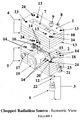
- the three major components of the device of the present invention i.e., the radiation source component 1, the chopper component 2, and the optical fiber connector component 3 are illustrated.
- the housing 4 for radiation source component 1, the housing 5 for chopper component 2, and connector 6 of optical fiber connector component 3 must each be made of a material which will withstand the environment in which the device is to be used and which is sufficiently rigid to support the elements of each of these components in a manner such that those elements will not move or shift during use of the chopped radiation source.
- Housings 4 and 5 and connector 6 are each preferably made with a metal such as aluminum, stainless steel or brass, but any other materials which are sufficiently strong and durable enough to withstand the conditions under which the device will be used may also be employed.
- the housings 4 and 5 shown in Figures 1 and 2 were made of aircraft grade aluminum, alloy 6061, metal plates which had been laser cut to accommodate the elements to be included in that housing. These plates were then stacked and bonded together. Although not a required feature of the invention, holes 24 into which screws may be inserted are shown in Figure 1 to illustrate one method for mounting the device of the present invention to a bench or post or other surface at the location where the device is to be used. Other means for holding the stacked plates and mounting the housing formed by such plates will be apparent to those skilled in the art. It would also be possible to "mold" sections of the housing(s) and attach it/them by any of the techniques known to those skilled in the art.
- the housings 4 and 5 must be at least large enough that all of the required components will fit within the housing(s) in a manner such that each of those components may function properly and will not move in an unintended manner during use. It is, of course, desirable that the housings be as small as possible for reasons of space and economy but there is no technical limitation with respect to the maximum size of the housings.
- a collimated radiation source 7 is positioned in an opening which is large enough to accommodate that radiation source. Radiation source 7 must remain stationary in housing 4. It is preferred that radiation source 7 be maintained stationary by making the opening into which radiation source 7 is placed sufficiently large to allow it to be placed in that housing 4 but small enough that radiation source 7 will not be free to move around. It is, however, possible to make radiation source 7 stationary by inserting radiation source 7 into a casing or base permanently mounted to housing 4 which casing or base has been designed to hold the radiation source in place. Radiation source 7 may be any source of visible, ultraviolet and/or near infrared (“NIR”) radiation known to those skilled in the art.
- NIR near infrared
- the radiation emitted by radiation source 7 be collimated, however, it is within the scope of the present invention to use any source of radiation. Radiation which is not collimated when emitted may be made collimated by techniques known to those skilled in the art, such as passage through an aspheric lens. Examples of preferred radiation sources include tungsten filament lamps and light emitting diodes. Selection of an appropriate radiation source will, of course, be dependent upon the particular application for which the chopped optical source will be used.
- the intensity of the radiation source be held at a constant level. While intensity adjustment is not necessary when the radiation source is selected to meet the specific requirements for that optical chopper or when that radiation source will be replaced before it nears the end of its useful life, it is generally advantageous to include means for adjusting the radiation intensity because such adjustability allows greater flexibility in selection of the radiation source and the ability to continue use of the radiation source after it has passed its peak performance.
- radiation intensity adjustment may be accomplished by monitoring the radiation from source 7 with detector 8 and using the output of detector 8 to drive a servo feedback loop (not shown) controlling the radiation source 7 drive.
- the set point of the source 7 drive may be adjusted by means of an adjustable optical iris 9 (also shown in Figure 2). It is, of course, possible to operate the chopped radiation source assembly without detector 8 and iris 9. However, it is preferred that these elements or some other elements known to be useful for adjusting radiation intensity be included in radiation source component 1.
- any of the known radiation detectors which is capable of detecting radiation at the wavelengths selected for use in the device of the present invention may be used as detector 8.
- Preferred detectors include phototransistors and photoconductive or photovoltaic silicon diodes.
- Any means for increasing or decreasing the amount of radiation emitted from radiation source 7 may be used as radiation adjuster or iris 9.
- Suitable adjustment means are known to those skilled in the art. Such adjustment means include a fine thread screw.
- radiation source 7 is positioned in housing 4 so that the emitted collimated radiation will reach beam director 10.
- Beam director 10 is employed in this embodiment of the invention because the condensing means 11 and optical fiber 12 are not on axis with source 7. Beam director 10 need not be included in radiation source component 1, however, if condensing means 11 and optical fiber 12 are on the same axis as the collimated radiation emitted by radiation source 7.
- beam director 10 is positioned in housing 4 so that it can receive radiation from radiation source 7 and direct that received radiation to radiation condensing means 11. It would, however, also be possible to position beam director 10 in housing 5 provided that beam director 10 would still be capable of receiving collimated radiation and directing such received radiation to the means for directing the collimated radiation to a focal point.
- Beam director 10 may be any of the known means for directing radiation such as mirrors or prisms. Preferred beam directors include beam steering prisms and mirrors. When used, beam director 10 should be at least large enough to capture the collimated radiation, preferably, it will have a width which is approximately equal to the diameter of radiation source 7.
- the radiation condensing means 11 need not be positioned in housing 4 as shown in Figure 2. Radiation condensing means 11 may also be positioned at any point where it is capable of receiving the collimated radiation emitted from radiation source 7 and condensing that radiation to a focal point. It is preferred, however, that radiation condensing means 11 be located in housing 4 at a point below beam director 10.
- Radiation condensing means 11 may be any of the known radiation condensers. Ball lenses, particularly sapphire ball lenses having diameters of from 1 to 10 mm are preferred. Condensing means 11 condenses the radiation to a focal point (not shown) at which optical fiber 12 is positioned to receive that radiation.
- alignment posts 13 Located at the base of housing 4 are alignment posts 13 (more clearly illustrated in Figure 2).
- the alignment posts 13 are positioned to fit into receiving cavities 14 located in housing 5 and thereby form the complete housing for the chopped optical source of the present invention. It is also within the scope of the present invention to position receiving cavities 14 at the base of housing 4 and alignment posts 13 at the top surface of housing 5.
- the number of alignment posts 13 and receiving cavities 14, if used, will generally be at least 2 alignment posts and 2 receiving cavities, preferably, at least three posts and 3 cavities, most preferably, 4 alignment posts and 4 receiving cavities.
- These alignment posts 13 and receiving cavities 14 are not essential features of the present invention but they are advantageously included because they facilitate proper alignment of the housings 4 and 5 and thus proper alignment of the elements included in those housings.
- the alignment posts 13 may be made of any material which will withstand the conditions of use. Metals such as rolled metal pins are particularly preferred. Alignment posts 13 and cavities 14 will be sufficiently long or deep that the completed housing will remain intact and both housings 4 and 5 will not move or shift during use.
- a reed 15 which is capable of vibrating is positioned in housing 5 so that the movement of chopper flag 18 will chop the beam entering optical fiber 12.
- reed 15 is positioned so that it is vertical with respect to the opening in housing 5. Such vertical positioning is preferred.
- One end of reed 15 is capable of relatively free movement while the reed's movement at the other end is restricted by supports 16 and the means for adjusting chopper duty cycle 17.
- Chopper flag 18 may be formed from the terminal portion of reed 15 or it may be attached to the movable end of reed 15.
- the chopper flag 18 was formed by twisting the terminal portion of reed 15 ninety degrees. Any of the chopper flags known to those skilled in the art may, however, be used.
- the chopper flag 18 shown in Figure 1 is particularly advantageous in that there is no risk of separation of the chopper flag from the reed.
- Reed 15 may be made of any flexible material which can be made to vibrate. Suitable materials include ferrous metals, spring steel, and sufficiently stiff polymer film. Ferrous metals are preferred when the means for causing the reed to vibrate is a solenoid coil. Any of the known piezoelectric resonating reeds may also be used as reed 15. Where a piezoelectric resonating reed is used, the preferred actuating material is a polyvinylidene fluoride such as that which is commercially available under the designation Kynar PVDF.
- Reed 15 should generally be long enough that the reed 15 with, chopper flag 18 will have a natural resonance between 100 and 1000 Hz, and have a deflection greater than twice the diameter of optical fiber 12.
- the reed length, thickness, width, Young's modulus of the reed material, or weight of the chopper flag 18 may be varied to achieve the desired frequency.
- the optimum resonance frequency of the reed depends upon the principal detector used in the spectrometer or photometer or other analytical device into which the chopped radiation source of the present invention will be incorporated. For a lead sulfide detector, the optimum resonance frequency is 600 Hz.
- the vibrating reed was fabricated from spring steel stock approximately 1.6 inches (4.0 cm) long, 0.19 inches (0.5 cm) wide, and .023 inches (0.058 cm) thick.
- the vibrating reed portion beyond the supports 16 was approximately 1.0 inches (2.5 cm) long and 0.09 inches (0.23 cm) wide.
- the chopper flag 18 portion was formed from the terminal portion of reed 15 and was 0.15 inches (0.38 cm) long and 0.19 inches (0.48 cm) wide. This reed/flag assembly resonated at approximately 450 Hz.
- Means for causing reed 15 to vibrate are well known in the art.
- vibration of reed 15 is induced by solenoid 19.
- a piezoelectric resonating reed as reed 15.
- solenoid 19 is not needed to cause vibration of the reed and the solenoid 19 can be omitted from the chopping component.
- the chopper duty cycle may be adjusted by any of the techniques known to those skilled in the art.
- the chopper duty cycle adjuster 17 shown in Figures 1 and 2 is a screw which when turned sufficiently applies pressure to or removes pressure from reed 15. Application or withdrawal of pressure on reed 15 between supports 16 causes the reed to bend and chopper flag 18 to change its position.
- chopper flag 18 When chopper flag 18 is positioned between radiation condensing means 11 and the focal point at which optical fiber 12 receives the condensed radiation in a manner such that the edge of chopper flag 18 at rest is aligned over the center of the optical fiber 12 and blocks 50% of the optical fiber face, it will generate a 50% duty cycle on the chopped radiation from source 7.
- a change in the at rest position of chopper flag 18 changes the duty cycle of the chopped beam.
- a chopped radiation beam when detected and processed by a lock-in amplifier will produce a maximum signal with a 50% duty cycle.
- Optical fiber connector component 3 is made up of connector housing 6, optical fiber 12 and opening 22.
- Optical fiber 12 is positioned within connector housing 6 in a manner such that at least a portion of optical fiber 12 will be exposed at opening 22. It is preferred that optical fiber 12 be secured within connector housing 6 in some manner, preferably with an adhesive material of some sort. Clear epoxy is particularly preferred.
- optical fiber 12 terminates in the fiber connector housing 6 which is positioned at a location such that condensed, chopped radiation will be received by optical fiber 12 at the focal point of the radiation which has passed through condenser 11.
- optical fiber connector 6 is inserted into cavity 20 of housing 5.
- Fiber connector housing 6 is secured in place in housing 5 with screw 21. It could, however, also be made to snap or screw into place or be secured by means of an adhesive or in any other manner known to those skilled in the art.
- Opening 22 of connector housing 6 exposes the optical fiber 12 and any material present on the surface of that fiber (e.g., epoxy) to detector 23.
- opening 22 is shown as a V-shaped notch in Figures 1 and 2, no particular shape for opening 22 is required.
- Opening 22 could also be a straight mill cut on the surface of connector 3 or any other shape which exposes at least a portion of optical fiber 12. Opening 22 need not be any particular size but it is preferred that the opening be at least large enough to permit sufficient radiation to be detected by detector 23. In the device illustrated in Figures 1 and 2, opening 22 was large enough to expose 0.125 inches (0.317 cm) of optical fiber.
- optical fiber to be used in the apparatus of the present invention is based upon the particular type of radiation which is to be chopped and is within the skill of the art. For example, where the radiation being chopped is in the near infrared (NIR) range, glass fiber having a very low hydroxyl (OH) content is preferred because OH hydroxyl content absorbs around 1400 nm and would adversely affect transmission of the NIR radiation. However, where the radiation being chopped is in the ultraviolet (UV) range, the hydroxyl content of the optical fiber does not interfere with the transmission of UV radiation.
- the optical fiber used in the apparatus of the present invention will generally have a diameter of from about 300 to about 1000 ⁇ m, preferably from 400 to 600 ⁇ m and be capable of multimode ray propagation.
- Fiber 12 in connector component 3 may be used to connect the chopped radiation source of the present invention to a probe (not shown) to be inserted into the material or stream being evaluated. Any of the known probes may be used with the radiation chopping device of the present invention. Selection of the probe will be based upon the type of analysis being conducted and the nature of the material or stream being analyzed.
- Fiber 12 in connector component 3 may also be used to connect the chopped radiation source of the present invention with other analytical devices.
- the epoxy on the surface of optical fiber 12 is illuminated with rays entering fiber 12 at an angle greater than the fiber acceptance angle which have penetrated the cladding and then the epoxy.
- These illuminating rays can be used to monitor radiation that is falling on the face of the fiber without reducing the amount of radiation being transmitted within the fiber core.
- a device corresponding to that shown in Figures 1 and 2 was constructed of the following materials:
Abstract
Description
- The present invention relates to a chopped radiation source, preferably, a chopped optical radiation source which is useful in analytical devices such as photometers and spectrophotometers, particularly in photometers for monitoring chemical production processes.
- Photometric and spectrophotometric devices for analyzing materials and monitoring reaction processes are known and commercially available. These devices compare radiation emitted by a source with radiation from that same source which has been transmitted through and altered by the sample material being evaluated.
- One technique employed for improving the accuracy of measurements made with photometers and spectrophotometers is "chopping" of the radiation. In this technique, the radiation flow is interrupted at regular intervals or "chopped". A chopped signal is necessary for AC coupling of amplifier stages in order to improve thermal stability. A chopped signal allows the use of electronic filters tuned to the chopped frequency to reduce background noise. Use of a chopper reference signal allows signal processing, sometimes referred to as lock-in amplification, to reduce background noise.
- Electronic filters and a reference signal are employed, for example, in the signal comparison apparatus described in U.S. Patent 2,678,581. In this disclosed apparatus, a beam of light is interrupted or pulsed at some predetermined frequency by a motor-driven rotating shutter or chopper wheel. A rotating sectored mirror is used to deflect the light pulses along one of two paths, and effectively acting as a second chopper at a lower pulse rate. Two fixed mirrors direct the light pulses toward a second rotating sectored mirror, in phase with the first rotating sectored mirror, to direct light toward a light sensitive element. Various properties of a sample, such as spectral characteristics or reflectance characteristics, may be compared by means of suitable devices positioned in the path(s) of the directed light pulses. The light pulse repetition rate is made substantially greater than the beam switching rate by providing a number of open sectors in the shutter and by using complementary half-round sectored mirrors. The light pulses received by the light sensitive element are converted to electrical pulses, which are capacitatively coupled between amplifier stages to eliminate temperature dependent DC drift. The signal is passed through electronic filters tuned to the chopper frequency to restrict bandwidth and reduce background noise. The signal is then processed by a lock-in amplifier that is mechanically synchronized with the chopping rate of the beam switching sectored mirrors. This results in decreased bandwidth, decreased noise and increased sensitivity.
- One disadvantage of using a rotating chopper wheel such as that disclosed in U.S. 2,678,581 is the wear on the moving parts and chopper frequency stability. A tuning fork chopper, however, has no wearing movable parts and has a natural resonant frequency. For these reasons, a tuning fork chopper has been used in a number of deep space experiments where reliability is essential. Such a chopper is made in the USA by Electro-Optical Products Corporation and available from Boston Electronics Corporation. However, a tuning fork chopper is not suitable for use in all applications, particularly where there are space limitations. A vibrating reed chopper is used for those applications in which there are spatial constraints because it can be packaged in a smaller space than a tuning fork chopper.
- Optical choppers have also been used in devices such as the infrared thermometer disclosed in U.S. Patent 5,653,537 in which light emitted from an object is conveyed to a detector via fiber optic cable. The detector generates electrical outputs. These outputs or signals are then amplified and linearized. Unlike the prior art pyrometers, however, the pyrometers disclosed in this patent do not continuously collect and repeatedly chop the collected light before it enters the detectors. Rather, the collected infrared light is reflected off of a dichroic mirror and then passed through a piezoelectric chopper to chop the infrared light. Chopping is achieved through oscillation of a vibrating reed driven by piezoelectric elements. The chopped infrared light then enters a fiber optic cable and is relayed via that cable to an infrared detector which re-focuses the light and then beamsplits the infrared light into two broad wavelength bands. One of these two broad wavelength bands is narrowed by an optical filter and detected by an infrared detector. The other broad wavelength band is directly detected by another infrared detector whose upper wavelength cutoff limits the wavelength band. The detectors generate an AC signal which is then amplified and linearized before being relayed to an analog to digital converter which generates the signal sent to a microprocessor.
- In these and most other known photometric, spectrophotometric and pyrometric devices, alignment of the light source with the means for relaying that light to the sample and to the detector is one factor which influences the accuracy of the measurement and restricts the locations at which such devices must be placed to sites remote from the reactors in which chemical reactions are being conducted. The known devices also present problems with adjustment of the duty cycle of the chopping device. Use of moving parts subject to wear and tear also introduces the potential for inaccuracy and reliability problems.
- It would therefore be advantageous to develop a chopped radiation source assembly which could be readily included in photometric, spectrophotometric and other types of analytical devices even when those devices are positioned in production areas without the need for realignment of light source with the chopper on a continuing basis or interruption of measurement for replacement of worn moving parts after a limited number of uses.
- It is an object of the present invention to provide a chopped radiation source, preferably, an optical radiation source which can be readily incorporated into analytical devices even when the analytical devices are located in production environments.
- It is another object of the present invention to provide a chopped radiation source, preferably, an optical radiation source with reduced drift and improved signal to noise ratio.
- It is a further object of the present invention to provide a chopped radiation source, preferably, an optical radiation source which is characterized by ease of alignment of the radiation source and adjustment of chopper duty cycle.
- It is also an object of the present invention to provide a chopped radiation source, preferably, an optical radiation source having a minimum number of moving parts.
- It is a further object of the present invention to provide a chopped radiation source having an integrated detector to control the intensity of the radiation.
- It is another object of the present invention to provide a chopped radiation source having an integrated means of coupling the chopped radiation from the source into an optical fiber for transfer to a remote location.
- It is also an object of the present invention to provide a chopped radiation source having a means for extracting a portion of the chopped beam from the radiation source that is coupled into an optical fiber without reducing the total energy throughput of the fiber.
- It is a further object of the present invention to provide a chopped radiation source having an integrated detector which is driven by an extracted beam from the fiber to output an electrical pulse in phase with the chopper to synchronize a lock-in amplifier.
- These and other objects which will be apparent to those skilled in the art are accomplished by the device of the present invention which is formed by housing the radiation source, optical chopping and optical fiber connector components described more fully herein in a manner such that those components remain in position during use.
-
- Figure 1 is an isometric view of one embodiment of the chopped radiation source of the present invention in which the radiation source component, the chopping component, and the optical fiber connector component are shown in detail.
- Figure 2 is a front view of the embodiment of the chopped radiation source shown in Figure 1.
- The present invention relates to a chopped radiation (preferably, optical radiation) source which is suitable for use in photometers, spectrophotometers and other analytic devices in which chopping of radiation is used to enhance instrument accuracy or performance.
- The chopped radiation source of the present invention is composed of (1) a radiation source component, (2) a chopper component, and (3) an optical fiber connector component. Each of these components is positioned in a housing in a manner such that the elements of each of these components will not move in an unintended manner during use.
- The key elements of the radiation source component are (a) a radiation source and (b) means for directing the radiation emitted by the source to a focal point. In the event that the radiation emitted by the radiation source in not collimated or collimated to the desired extent, a means for collimating the radiation may be advantageously included in the radiation source component.
- The key elements of the chopping component include (a) a reed which is capable of resonating and which is fixed at one end and free to move at the other end, (b) a chopper flag positioned at an angle (preferably a 90° angle) with respect to the movable end of the reed, (c) means for adjusting pressure on the reed, (d) means for causing the reed to vibrate at its resonant frequency, and (e) a radiation detector. The pressure adjusting means (c) should make it possible to align the chopper flag when it is at rest with the focal point of the radiation from the radiation source component (1). The radiation detector (e) should be positioned so that it will receive chopped radiation emanating from the optical fiber connector component.
- The key elements of the optical fiber connector component include (a) optical fiber and (b) a housing with (c) an opening. The optical fiber is positioned so that it terminates at the focal point of the radiation from the radiation source component (1). The housing for the optical fiber encases most of the optical fiber and will generally serve as the means for holding the optical fiber in the correct position. The opening (c) in housing (b) leaves a minor portion of the optical fiber exposed. This opening (c) is positioned so that any radiation emitted through that opening can be detected by radiation detector (e) of component (2).
- In one of the preferred embodiments of the present invention, means for detecting the intensity of the radiation emitted by the source and means for adjusting the amount of radiation to be chopped are included in the radiation source component.
- In another preferred embodiment of the present invention, the chopper flag is formed from a section of the resonating reed at the movable end of that reed.
- In another embodiment of the invention, a lock-in amplifier is synchronized with the output of an electrical pulse which is in phase with the chopper which electrical pulse is derived from the radiation emitted at the opening of the optical fiber component housing.
- The chopped radiation source of the present invention will be described in greater detail with reference to Figures 1 and 2.
- In each of Figures 1 and 2, the three major components of the device of the present invention, i.e., the
radiation source component 1, thechopper component 2, and the opticalfiber connector component 3 are illustrated. Thehousing 4 forradiation source component 1, thehousing 5 forchopper component 2, andconnector 6 of opticalfiber connector component 3 must each be made of a material which will withstand the environment in which the device is to be used and which is sufficiently rigid to support the elements of each of these components in a manner such that those elements will not move or shift during use of the chopped radiation source.Housings connector 6 are each preferably made with a metal such as aluminum, stainless steel or brass, but any other materials which are sufficiently strong and durable enough to withstand the conditions under which the device will be used may also be employed. Thehousings housings - In
housing 4, a collimatedradiation source 7 is positioned in an opening which is large enough to accommodate that radiation source.Radiation source 7 must remain stationary inhousing 4. It is preferred thatradiation source 7 be maintained stationary by making the opening into whichradiation source 7 is placed sufficiently large to allow it to be placed in thathousing 4 but small enough thatradiation source 7 will not be free to move around. It is, however, possible to makeradiation source 7 stationary by insertingradiation source 7 into a casing or base permanently mounted tohousing 4 which casing or base has been designed to hold the radiation source in place.Radiation source 7 may be any source of visible, ultraviolet and/or near infrared ("NIR") radiation known to those skilled in the art. It is preferred that the radiation emitted byradiation source 7 be collimated, however, it is within the scope of the present invention to use any source of radiation. Radiation which is not collimated when emitted may be made collimated by techniques known to those skilled in the art, such as passage through an aspheric lens. Examples of preferred radiation sources include tungsten filament lamps and light emitting diodes. Selection of an appropriate radiation source will, of course, be dependent upon the particular application for which the chopped optical source will be used. - It is desirable that the intensity of the radiation source be held at a constant level. While intensity adjustment is not necessary when the radiation source is selected to meet the specific requirements for that optical chopper or when that radiation source will be replaced before it nears the end of its useful life, it is generally advantageous to include means for adjusting the radiation intensity because such adjustability allows greater flexibility in selection of the radiation source and the ability to continue use of the radiation source after it has passed its peak performance.
- In the embodiment of the invention illustrated in Figure 1, radiation intensity adjustment may be accomplished by monitoring the radiation from
source 7 withdetector 8 and using the output ofdetector 8 to drive a servo feedback loop (not shown) controlling theradiation source 7 drive. The set point of thesource 7 drive may be adjusted by means of an adjustable optical iris 9 (also shown in Figure 2). It is, of course, possible to operate the chopped radiation source assembly withoutdetector 8 and iris 9. However, it is preferred that these elements or some other elements known to be useful for adjusting radiation intensity be included inradiation source component 1. - Any of the known radiation detectors which is capable of detecting radiation at the wavelengths selected for use in the device of the present invention may be used as
detector 8. Preferred detectors include phototransistors and photoconductive or photovoltaic silicon diodes. Any means for increasing or decreasing the amount of radiation emitted fromradiation source 7 may be used as radiation adjuster or iris 9. Suitable adjustment means are known to those skilled in the art. Such adjustment means include a fine thread screw. - In the embodiment of the invention illustrated in Figure 1,
radiation source 7 is positioned inhousing 4 so that the emitted collimated radiation will reachbeam director 10.Beam director 10 is employed in this embodiment of the invention because the condensing means 11 andoptical fiber 12 are not on axis withsource 7.Beam director 10 need not be included inradiation source component 1, however, if condensing means 11 andoptical fiber 12 are on the same axis as the collimated radiation emitted byradiation source 7. - In the apparatus illustrated in Figure 1,
beam director 10 is positioned inhousing 4 so that it can receive radiation fromradiation source 7 and direct that received radiation to radiation condensing means 11. It would, however, also be possible to positionbeam director 10 inhousing 5 provided thatbeam director 10 would still be capable of receiving collimated radiation and directing such received radiation to the means for directing the collimated radiation to a focal point.Beam director 10 may be any of the known means for directing radiation such as mirrors or prisms. Preferred beam directors include beam steering prisms and mirrors. When used,beam director 10 should be at least large enough to capture the collimated radiation, preferably, it will have a width which is approximately equal to the diameter ofradiation source 7. - The radiation condensing means 11 need not be positioned in
housing 4 as shown in Figure 2. Radiation condensing means 11 may also be positioned at any point where it is capable of receiving the collimated radiation emitted fromradiation source 7 and condensing that radiation to a focal point. It is preferred, however, that radiation condensing means 11 be located inhousing 4 at a point belowbeam director 10. - Radiation condensing means 11 may be any of the known radiation condensers. Ball lenses, particularly sapphire ball lenses having diameters of from 1 to 10 mm are preferred. Condensing means 11 condenses the radiation to a focal point (not shown) at which
optical fiber 12 is positioned to receive that radiation. - Located at the base of
housing 4 are alignment posts 13 (more clearly illustrated in Figure 2). The alignment posts 13 are positioned to fit into receivingcavities 14 located inhousing 5 and thereby form the complete housing for the chopped optical source of the present invention. It is also within the scope of the present invention to position receivingcavities 14 at the base ofhousing 4 andalignment posts 13 at the top surface ofhousing 5. The number ofalignment posts 13 and receivingcavities 14, if used, will generally be at least 2 alignment posts and 2 receiving cavities, preferably, at least three posts and 3 cavities, most preferably, 4 alignment posts and 4 receiving cavities. These alignment posts 13 and receivingcavities 14 are not essential features of the present invention but they are advantageously included because they facilitate proper alignment of thehousings cavities 14 will be sufficiently long or deep that the completed housing will remain intact and bothhousings - A
reed 15 which is capable of vibrating is positioned inhousing 5 so that the movement ofchopper flag 18 will chop the beam enteringoptical fiber 12. In the embodiment of the invention illustrated in Figure 1,reed 15 is positioned so that it is vertical with respect to the opening inhousing 5. Such vertical positioning is preferred. One end ofreed 15 is capable of relatively free movement while the reed's movement at the other end is restricted bysupports 16 and the means for adjustingchopper duty cycle 17. At the end ofreed 15 which is capable of relatively free movement is locatedchopper flag 18.Chopper flag 18 may be formed from the terminal portion ofreed 15 or it may be attached to the movable end ofreed 15. In the chopper assembly illustrated in Figure 1, thechopper flag 18 was formed by twisting the terminal portion ofreed 15 ninety degrees. Any of the chopper flags known to those skilled in the art may, however, be used. Thechopper flag 18 shown in Figure 1 is particularly advantageous in that there is no risk of separation of the chopper flag from the reed. -
Reed 15 may be made of any flexible material which can be made to vibrate. Suitable materials include ferrous metals, spring steel, and sufficiently stiff polymer film. Ferrous metals are preferred when the means for causing the reed to vibrate is a solenoid coil. Any of the known piezoelectric resonating reeds may also be used asreed 15. Where a piezoelectric resonating reed is used, the preferred actuating material is a polyvinylidene fluoride such as that which is commercially available under the designation Kynar PVDF.Reed 15 should generally be long enough that thereed 15 with,chopper flag 18 will have a natural resonance between 100 and 1000 Hz, and have a deflection greater than twice the diameter ofoptical fiber 12. In order to adjust the resonance frequency ofreed 15, the reed length, thickness, width, Young's modulus of the reed material, or weight of thechopper flag 18 may be varied to achieve the desired frequency. The optimum resonance frequency of the reed depends upon the principal detector used in the spectrometer or photometer or other analytical device into which the chopped radiation source of the present invention will be incorporated. For a lead sulfide detector, the optimum resonance frequency is 600 Hz. - In the device illustrated in Figures 1 and 2, the vibrating reed was fabricated from spring steel stock approximately 1.6 inches (4.0 cm) long, 0.19 inches (0.5 cm) wide, and .023 inches (0.058 cm) thick. The vibrating reed portion beyond the
supports 16 was approximately 1.0 inches (2.5 cm) long and 0.09 inches (0.23 cm) wide. Thechopper flag 18 portion, was formed from the terminal portion ofreed 15 and was 0.15 inches (0.38 cm) long and 0.19 inches (0.48 cm) wide. This reed/flag assembly resonated at approximately 450 Hz. - Means for causing
reed 15 to vibrate are well known in the art. In Figures 1 and 2, vibration ofreed 15 is induced bysolenoid 19. It is also possible to use a piezoelectric resonating reed asreed 15. When a piezoelectric resonating reed is used,solenoid 19 is not needed to cause vibration of the reed and thesolenoid 19 can be omitted from the chopping component. - The chopper duty cycle may be adjusted by any of the techniques known to those skilled in the art. The chopper
duty cycle adjuster 17 shown in Figures 1 and 2 is a screw which when turned sufficiently applies pressure to or removes pressure fromreed 15. Application or withdrawal of pressure onreed 15 betweensupports 16 causes the reed to bend andchopper flag 18 to change its position. Whenchopper flag 18 is positioned between radiation condensing means 11 and the focal point at whichoptical fiber 12 receives the condensed radiation in a manner such that the edge ofchopper flag 18 at rest is aligned over the center of theoptical fiber 12 and blocks 50% of the optical fiber face, it will generate a 50% duty cycle on the chopped radiation fromsource 7. A change in the at rest position ofchopper flag 18 changes the duty cycle of the chopped beam. A chopped radiation beam when detected and processed by a lock-in amplifier will produce a maximum signal with a 50% duty cycle. - Optical
fiber connector component 3 is made up ofconnector housing 6,optical fiber 12 andopening 22.Optical fiber 12 is positioned withinconnector housing 6 in a manner such that at least a portion ofoptical fiber 12 will be exposed atopening 22. It is preferred thatoptical fiber 12 be secured withinconnector housing 6 in some manner, preferably with an adhesive material of some sort. Clear epoxy is particularly preferred. - In the chopped radiation source shown in Figures 1 and 2,
optical fiber 12 terminates in thefiber connector housing 6 which is positioned at a location such that condensed, chopped radiation will be received byoptical fiber 12 at the focal point of the radiation which has passed throughcondenser 11. In Figure 1,optical fiber connector 6 is inserted intocavity 20 ofhousing 5.Fiber connector housing 6 is secured in place inhousing 5 withscrew 21. It could, however, also be made to snap or screw into place or be secured by means of an adhesive or in any other manner known to those skilled in the art.Opening 22 ofconnector housing 6 exposes theoptical fiber 12 and any material present on the surface of that fiber (e.g., epoxy) todetector 23. Although opening 22 is shown as a V-shaped notch in Figures 1 and 2, no particular shape for opening 22 is required.Opening 22 could also be a straight mill cut on the surface ofconnector 3 or any other shape which exposes at least a portion ofoptical fiber 12.Opening 22 need not be any particular size but it is preferred that the opening be at least large enough to permit sufficient radiation to be detected bydetector 23. In the device illustrated in Figures 1 and 2, opening 22 was large enough to expose 0.125 inches (0.317 cm) of optical fiber. - It is known to those skilled in the art that not all radiation beam rays incident on the end face of an optical fiber will successfully propagate along the inner core of the fiber and emerge at the other end. Only those rays within the fiber acceptance cone angle will propagate along the inner core. Those rays outside of the acceptance cone angle will refract into the fiber cladding and be lost. It is these "lost" rays which are detected by
radiation detector 23 throughopening 22. Where the optical fiber is held in place withinhousing 6 by an adhesive, a portion of the rays that refract into the cladding will penetrate the adhesive (preferably, epoxy) cementing thefiber 12 to theconnector housing 6 and illuminate the epoxy or adhesive. The radiation that is illuminating the epoxy may be readily detected byradiation detector 23 which detects the phase of chopped radiation cycle modulated byoptical chopper flag 18. - Selection of the optical fiber to be used in the apparatus of the present invention is based upon the particular type of radiation which is to be chopped and is within the skill of the art. For example, where the radiation being chopped is in the near infrared (NIR) range, glass fiber having a very low hydroxyl (OH) content is preferred because OH hydroxyl content absorbs around 1400 nm and would adversely affect transmission of the NIR radiation. However, where the radiation being chopped is in the ultraviolet (UV) range, the hydroxyl content of the optical fiber does not interfere with the transmission of UV radiation. The optical fiber used in the apparatus of the present invention will generally have a diameter of from about 300 to about 1000 µm, preferably from 400 to 600 µm and be capable of multimode ray propagation.
-
Fiber 12 inconnector component 3 may be used to connect the chopped radiation source of the present invention to a probe (not shown) to be inserted into the material or stream being evaluated. Any of the known probes may be used with the radiation chopping device of the present invention. Selection of the probe will be based upon the type of analysis being conducted and the nature of the material or stream being analyzed. -
Fiber 12 inconnector component 3 may also be used to connect the chopped radiation source of the present invention with other analytical devices. - At
section 22 offiber connector component 3 illustrated in Figures 1 and 2, the epoxy on the surface ofoptical fiber 12 is illuminated withrays entering fiber 12 at an angle greater than the fiber acceptance angle which have penetrated the cladding and then the epoxy. These illuminating rays can be used to monitor radiation that is falling on the face of the fiber without reducing the amount of radiation being transmitted within the fiber core. - Having thus described our invention, the following Example is given as being illustrative thereof.
- A device corresponding to that shown in Figures 1 and 2 was constructed of the following materials:
-
Housing 4 - 6061 alloy aluminum plates which were laser cut to accommodate elements of the
radiation source component 1, stacked and joined together with epoxy and steel roll pins. -
Housing 5 - 6061 alloy aluminum plates which were laser cut to accommodate the elements of
chopper component 2, stacked and joined together with epoxy and steel roll pins. -
Housing 6 - Fabricated from a standard fiber optic SMA Connector
-
Radiation source 7 - Tungsten filament lamp which emitted radiation at wavelengths of from 400 nm to 2500 nm which is commercially available from Gilway Lamps (# I1025).
- Radiation intensity
- Detector which is commercially available from
-
detector 8 - DigiKey (Part # QSC114-ND).
- Radiation intensity adjuster 9
- 4/40 machine screw
-
Beam director 10 - A first surface mirror having a width of 0.25 inches.(0.635 cm).
-
Radiation condenser 11 - A sapphire ball lens having a diameter of 0.25 inches (0.635 cm) which is commercially available from Edmund Scientific (#H43-831).
-
Optical fiber 12 - 500 um diameter low OH glass fiber from RoMack Fiber Optics
- Alignment posts 13
- 1/16 inch steel roll pins having a length of 0.625 inches (1.59 cm).
- Receiving
cavities 14 - Cut in
housing 5, 0.125 inches deep (0.318 cm). -
Reed 15 - Fabricated from Stihl rewind spring (Part # LB05A02) measuring 0.187 inches (0.475 cm) wide by 0.024 inches (0.061 cm) thick. The first section in contact with
bridge posts 16 measured 0.438 inches (1.11 cm) long by 0.187 inches (0.475 cm) wide. The second section which was free to move measured 1.00 inch (2.54 cm) long by 0.188 inches (0.47625 cm) wide. - Bridge posts 16
- 1/32 inch steel pins which were 0.25 inches long (0.635 cm).
- Chopper
duty cycle adjuster 17 - 4/40 machine screw
-
Chopper flag 18 - Terminal section of
reed 15 at a 90° angle to the stationary portion ofreed 15 and measuring 0.150 inches (0.381 cm) long and 0.189 inches (0.48 cm) wide. -
Solenoid 19 - Solenoid coil removed from a Tyco relay (Part # T90S1D12-5)
-
Cavity 20 - Cavity cut out of
housing 5 measuring 0.125 inches (0.317 cm) in diameter and 0.5 inches (1.27 cm) long. -
Connector Screw 21 - 4/40 machine screw
-
Opening 22 - Opening exposing 0.125 inches (0.317 cm) of optical fiber machined from
housing 6. -
Phase Detector 23 - Detector which is commercially available from DigiKey (Part # QSC114-ND).
- Although the invention has been described in detail in the foregoing, it is to be understood that such detail is solely for that purpose and that variations can be made therein by those skilled in the art without departing from the spirit and scope of the invention except as it may be limited by the claims.
Claims (34)
- A chopped radiation source comprising:a) a radiation source component comprising:1) a radiation source in a fixed position2) means for collimating radiation emitted by (1), if the radiation emitted by (1) is not already collimated, and(3) means for directing collimated radiation to a focal point,b) a chopping component comprising:(1) a reed which at one end is capable of moving freely and at the other end is relatively fixed,(2) a chopper flag positioned at a 90° angle with respect to the end of the reed which is capable of moving freely,(3) a means for adjusting pressure on the reed in a manner such that the chopper flag when at rest will be aligned with the focal point of the collimated radiation,(4) means for exciting the reed sufficiently to cause the reed to vibrate at its resonant frequency, and(5) a radiation detector positioned to receive and detect chopped radiation emanating from an optical fiber connector component,andc) the optical fiber connector component comprising:in which each element of each of components (1), (2) and (3) is maintained in its proper position within a housing.(1) optical fiber positioned so that one end receives radiation at the focal point of the collimated radiation,(2) a housing for the optical fiber with(3) an opening positioned so that radiation emitted through the opening will be received by the detector in chopping component b)
- A chopped optical radiation source comprising:a) a radiation source component comprising a first housing composed of a material which is sufficiently rigid to support elements present therein in a manner such that those elements will not drift or move during use in which the elements comprise:(1) an optical radiation source,(2) means for collimating radiation from (1), if necessary, and(3) means for directing collimated radiation to a focal point,(4) optionally, means for detecting intensity of radiation from (1),(5) optionally, means for adjusting intensity of the radiation from (1),b) a chopping component comprising a second housing composed of a material which is sufficiently rigid to support elements present therein in a manner such that those elements will not drift or move during use in which the elements comprise:(6) a reed with a first end fixed to a wall of the second housing and a second end capable of moving freely,(7) a chopper flag positioned at a right angle to the second end of the reed and which is positioned to receive vibration originating from the reed to chop optical radiation from source (1) at the focal point,(8) means for adjusting pressure on the reed to align the chopper flag's resting point, with the collimated radiation and the focal point,(9) a means for causing the reed to vibrate at the reed's resonant frequency,(10) a cavity for holding an optical fiber connector component such that an optical fiber is positioned at the focal point,(11) a means for securing the optical fiber connector component when it is positioned in cavity (10),(12) a radiation detector positioned to receive and detect chopped radiation emanating from an opening in the optical fiber connector component when the connector component is positioned in cavity (10), andc) an optical fiber connector component capable of being positioned in cavity (10) comprising a third housing composed of a material which is sufficiently rigid to support elements present therein in a manner such that those elements will not drift or move during use which elements comprise:(13) an optical fiber with end face positioned at the focal point to receive chopped optical radiation from chopping component (2) and to transmit received optical radiation to a remote location, and(14) an opening in the housing of the optical fiber connector component which opening is positioned sufficiently close to the fiber's end face to emit radiation that has entered the fiber at an angle outside of the fiber's acceptance cone angle,andd) a means for aligning the first housing with the second housing.
- The chopped radiation source of Claim 1 in which the radiation source is a tungsten filament lamp.
- The chopped radiation source of Claim 1 in which the radiation source is a lamp which emits near infrared radiation.
- The chopped radiation source of Claim 2 in which each of the first and second housings is composed of metal.
- The chopped radiation source of Claim 2 in which each of the first and second housings is composed of stacked metal plates which have been bonded together.
- The chopped radiation source of Claim 1 in which directing means (3) is a beam steering prism.
- The chopped radiation source of Claim 1 in which directing means (3) is a beam steering mirror.
- The chopped radiation source of Claim 2 in which directing means (3) is a beam steering prism
- The chopped radiation source of Claim 1 in which the means for adjusting radiation intensity (5) is a bolt or screw.
- The chopped radiation source of Claim 1 in which the radiation source is a light emitting diode.
- The chopped radiation source of Claim 1 in which the radiation source is a light emitting diode capable of emitting ultraviolet, visible and near infrared radiation.
- The chopped radiation source of Claim 1 in which directing means (3) is a 45 degree beam steering prism.
- The chopped radiation source of Claim 1 in which directing means (3) is a flat mirror.
- The chopped radiation source of Claim 1 in which collimating means (2) is a sapphire ball lens.
- The chopped radiation source of Claim 15 in which the sapphire ball lens has a diameter of from 3 to 10 mm.
- The chopped radiation source of Claim 1 in which radiation detector (4) is a phototransistor.
- The chopped radiation source of Claim 1 in which radiation detector (4) is a photovoltaic or photoconductive diode.
- The chopped radiation source of Claim 2 in which alignment means (d) comprises posts mounted on the first housing which can be inserted into corresponding cavities present in the second housing.
- The chopped radiation source of Claim 1 in which the reed is made of spring steel.
- The chopped radiation source of Claim 1 in which the reed is from 15 to 50 mm in length, from 3 to 10 mm in height and from 0.2 to 0.8 mm thick.
- The chopped radiation of Claim 1 in which the chopper flag is an extension of the reed which has been formed by twisting the movable end of the reed by 90 degrees.
- The chopped radiation source of Claim 1 in which the reed is magnetically driven.
- The chopped radiation source of Claim 20 in which a solenoid coil is included in the chopping component to cause resonation of the reed.
- The chopped radiation source of Claim 1 in which the reed is a piezoelectric resonating reed.
- The chopped radiation source of Claim 22 in which the piezoelectric actuating material is polyvinylidene fluoride.
- The chopped radiation source of Claim 22 in which a pulsating AC or DC signal is used to provide resonance to the reed.
- The chopped radiation source of Claim 27 in which the AC or DC signal has a frequency between 30 and 1000 Hz.
- The chopped radiation source of Claim 27 in which the AC or DC signal has a frequency between 400 to 600 Hz.
- A photometer which includes the chopped radiation source of Claim 1.
- A photometer which includes the chopped radiation source of Claim 2.
- A method for monitoring a chemical reaction comprising:(a) inserting a probe (could use a flow through cell) which is connected to the photometer of Claim 30 into a reaction stream and(b) reviewing output from the photometer.
- A method for monitoring a chemical reaction comprising:(a) inserting a probe which is connected to the photometer of Claim 31 into a reaction stream and(b) reviewing output from the photometer
- A method for monitoring a chemical reaction comprising:(a) placing a flow through cell connected to the photometer of Claim 30 into a stream to be monitored and(b) reviewing output from the photometer.
Priority Applications (1)
| Application Number | Priority Date | Filing Date | Title |
|---|---|---|---|
| PL05023622T PL1655587T3 (en) | 2004-11-08 | 2005-10-28 | A chopped radiation source |
Applications Claiming Priority (1)
| Application Number | Priority Date | Filing Date | Title |
|---|---|---|---|
| US10/983,404 US7151265B2 (en) | 2004-11-08 | 2004-11-08 | Chopped radiation source |
Publications (2)
| Publication Number | Publication Date |
|---|---|
| EP1655587A1 true EP1655587A1 (en) | 2006-05-10 |
| EP1655587B1 EP1655587B1 (en) | 2008-10-15 |
Family
ID=35602868
Family Applications (1)
| Application Number | Title | Priority Date | Filing Date |
|---|---|---|---|
| EP05023622A Not-in-force EP1655587B1 (en) | 2004-11-08 | 2005-10-28 | A chopped radiation source |
Country Status (10)
| Country | Link |
|---|---|
| US (1) | US7151265B2 (en) |
| EP (1) | EP1655587B1 (en) |
| CN (1) | CN1782694A (en) |
| AT (1) | ATE411512T1 (en) |
| CA (1) | CA2525354C (en) |
| DE (1) | DE602005010367D1 (en) |
| ES (1) | ES2314541T3 (en) |
| MX (1) | MXPA05011816A (en) |
| PL (1) | PL1655587T3 (en) |
| PT (1) | PT1655587E (en) |
Families Citing this family (1)
| Publication number | Priority date | Publication date | Assignee | Title |
|---|---|---|---|---|
| CN106769866A (en) * | 2016-12-28 | 2017-05-31 | 吉林大学 | A kind of biochip objective table |
Citations (4)
| Publication number | Priority date | Publication date | Assignee | Title |
|---|---|---|---|---|
| GB823667A (en) * | 1956-09-19 | 1959-11-18 | White Dev Corp | Method and apparatus for reducing the effect of scattered light in monochromators |
| US3536910A (en) * | 1967-10-25 | 1970-10-27 | Ici Ltd | Beam-choppers for use in spectroscopes and like instruments |
| US6280100B1 (en) * | 1998-12-30 | 2001-08-28 | Mcdonnell Douglas Corporation | Fiber optic connector with micro-alignable sensing fiber and associated fabrication method |
| US20020071123A1 (en) * | 2000-10-12 | 2002-06-13 | Miller Richard L. | Photometric detection system having multiple path length flow cell |
Family Cites Families (5)
| Publication number | Priority date | Publication date | Assignee | Title |
|---|---|---|---|---|
| US2678581A (en) | 1949-11-30 | 1954-05-18 | Rca Corp | Signal comparison apparatus |
| US4011745A (en) * | 1974-07-26 | 1977-03-15 | Massachusetts Institute Of Technology | Semiconductor sensors |
| US4233512A (en) * | 1978-10-02 | 1980-11-11 | Norman C. Anderson | Thermometer for remotely measuring temperature |
| US5653537A (en) * | 1995-03-17 | 1997-08-05 | Ircon, Inc. | Non-contacting infrared temperature thermometer detector apparatus |
| US5678581A (en) * | 1995-10-06 | 1997-10-21 | United Microelectronics Corporation | Apparatus for cleaning an air pump silencer |
-
2004
- 2004-11-08 US US10/983,404 patent/US7151265B2/en active Active
-
2005
- 2005-10-28 AT AT05023622T patent/ATE411512T1/en not_active IP Right Cessation
- 2005-10-28 EP EP05023622A patent/EP1655587B1/en not_active Not-in-force
- 2005-10-28 ES ES05023622T patent/ES2314541T3/en active Active
- 2005-10-28 DE DE602005010367T patent/DE602005010367D1/en active Active
- 2005-10-28 PT PT05023622T patent/PT1655587E/en unknown
- 2005-10-28 PL PL05023622T patent/PL1655587T3/en unknown
- 2005-11-03 CA CA2525354A patent/CA2525354C/en not_active Expired - Fee Related
- 2005-11-03 MX MXPA05011816A patent/MXPA05011816A/en active IP Right Grant
- 2005-11-08 CN CNA2005101200294A patent/CN1782694A/en active Pending
Patent Citations (4)
| Publication number | Priority date | Publication date | Assignee | Title |
|---|---|---|---|---|
| GB823667A (en) * | 1956-09-19 | 1959-11-18 | White Dev Corp | Method and apparatus for reducing the effect of scattered light in monochromators |
| US3536910A (en) * | 1967-10-25 | 1970-10-27 | Ici Ltd | Beam-choppers for use in spectroscopes and like instruments |
| US6280100B1 (en) * | 1998-12-30 | 2001-08-28 | Mcdonnell Douglas Corporation | Fiber optic connector with micro-alignable sensing fiber and associated fabrication method |
| US20020071123A1 (en) * | 2000-10-12 | 2002-06-13 | Miller Richard L. | Photometric detection system having multiple path length flow cell |
Also Published As
| Publication number | Publication date |
|---|---|
| CA2525354A1 (en) | 2006-05-08 |
| MXPA05011816A (en) | 2007-08-08 |
| CA2525354C (en) | 2016-01-12 |
| PL1655587T3 (en) | 2009-04-30 |
| US7151265B2 (en) | 2006-12-19 |
| ES2314541T3 (en) | 2009-03-16 |
| US20060097181A1 (en) | 2006-05-11 |
| ATE411512T1 (en) | 2008-10-15 |
| EP1655587B1 (en) | 2008-10-15 |
| DE602005010367D1 (en) | 2008-11-27 |
| PT1655587E (en) | 2008-12-22 |
| CN1782694A (en) | 2006-06-07 |
Similar Documents
| Publication | Publication Date | Title |
|---|---|---|
| CA2529823C (en) | A process photometer | |
| EP2188604B1 (en) | Spectrometer for measuring moving sample material and the method | |
| US3994590A (en) | Discrete frequency colorimeter | |
| EP2019307A1 (en) | Method and gas sensor for performing quartz-enhanced photoacoustic spectroscopy | |
| EP0699898A2 (en) | A dual beam tunable spectrometer | |
| EP2383565A1 (en) | Optical device, analyzing apparatus and spectroscopic method | |
| KR101433497B1 (en) | Gas concentration monitor | |
| WO2001055706A1 (en) | Photothermic transducing spectroscopic analyzer | |
| JP2009025298A (en) | Optical cavity system having orthogonal input | |
| WO2008024344A2 (en) | Compact raman or fluorescence excitation system | |
| WO2015186407A1 (en) | Gas measurement device and measurement method | |
| EP0797091A1 (en) | Surface plasmon resonance sensor with interchangable optical element | |
| EP1655587B1 (en) | A chopped radiation source | |
| US11378450B2 (en) | Compact infrared spectrometer systems and methods for measuring vibrational spectrum of materials and substances | |
| KR101409620B1 (en) | Apparatus for Measuring Gas | |
| US5848090A (en) | Adjusted laser cavity resonator and method for preparing a laser resonator | |
| JPH05281041A (en) | Spectroscope | |
| JPH08327550A (en) | Raman spectrometer | |
| JPS62188919A (en) | Method and instrument for direct emission analysis by multistage laser excitation | |
| JPH10332585A (en) | Gas sensor | |
| KR102504516B1 (en) | Device for laser absorption spectroscopy analysis | |
| JPS6285847A (en) | Method and device for direct emission spectrochemical analysis of laser multistage excitation | |
| JPH051991A (en) | Probe for reflected light measurement device | |
| RU2186350C1 (en) | Device measuring temperature | |
| RU2186351C1 (en) | Device measuring physical parameters, predominantly temperature |
Legal Events
| Date | Code | Title | Description |
|---|---|---|---|
| PUAI | Public reference made under article 153(3) epc to a published international application that has entered the european phase |
Free format text: ORIGINAL CODE: 0009012 |
|
| AK | Designated contracting states |
Kind code of ref document: A1 Designated state(s): AT BE BG CH CY CZ DE DK EE ES FI FR GB GR HU IE IS IT LI LT LU LV MC NL PL PT RO SE SI SK TR |
|
| AX | Request for extension of the european patent |
Extension state: AL BA HR MK YU |
|
| 17P | Request for examination filed |
Effective date: 20061110 |
|
| 17Q | First examination report despatched |
Effective date: 20061207 |
|
| AKX | Designation fees paid |
Designated state(s): AT BE BG CH CY CZ DE DK EE ES FI FR GB GR HU IE IS IT LI LT LU LV MC NL PL PT RO SE SI SK TR |
|
| GRAP | Despatch of communication of intention to grant a patent |
Free format text: ORIGINAL CODE: EPIDOSNIGR1 |
|
| GRAS | Grant fee paid |
Free format text: ORIGINAL CODE: EPIDOSNIGR3 |
|
| GRAA | (expected) grant |
Free format text: ORIGINAL CODE: 0009210 |
|
| AK | Designated contracting states |
Kind code of ref document: B1 Designated state(s): AT BE BG CH CY CZ DE DK EE ES FI FR GB GR HU IE IS IT LI LT LU LV MC NL PL PT RO SE SI SK TR |
|
| REG | Reference to a national code |
Ref country code: CH Ref legal event code: EP Ref country code: GB Ref legal event code: FG4D |
|
| REG | Reference to a national code |
Ref country code: IE Ref legal event code: FG4D |
|
| REF | Corresponds to: |
Ref document number: 602005010367 Country of ref document: DE Date of ref document: 20081127 Kind code of ref document: P |
|
| REG | Reference to a national code |
Ref country code: RO Ref legal event code: EPE |
|
| REG | Reference to a national code |
Ref country code: PT Ref legal event code: SC4A Free format text: AVAILABILITY OF NATIONAL TRANSLATION Effective date: 20081211 |
|
| REG | Reference to a national code |
Ref country code: ES Ref legal event code: FG2A Ref document number: 2314541 Country of ref document: ES Kind code of ref document: T3 |
|
| PG25 | Lapsed in a contracting state [announced via postgrant information from national office to epo] |
Ref country code: AT Free format text: LAPSE BECAUSE OF FAILURE TO SUBMIT A TRANSLATION OF THE DESCRIPTION OR TO PAY THE FEE WITHIN THE PRESCRIBED TIME-LIMIT Effective date: 20081015 Ref country code: LT Free format text: LAPSE BECAUSE OF FAILURE TO SUBMIT A TRANSLATION OF THE DESCRIPTION OR TO PAY THE FEE WITHIN THE PRESCRIBED TIME-LIMIT Effective date: 20081015 Ref country code: BG Free format text: LAPSE BECAUSE OF FAILURE TO SUBMIT A TRANSLATION OF THE DESCRIPTION OR TO PAY THE FEE WITHIN THE PRESCRIBED TIME-LIMIT Effective date: 20090115 |
|
| REG | Reference to a national code |
Ref country code: PL Ref legal event code: T3 |
|
| REG | Reference to a national code |
Ref country code: HU Ref legal event code: AG4A Ref document number: E004811 Country of ref document: HU |
|
| PG25 | Lapsed in a contracting state [announced via postgrant information from national office to epo] |
Ref country code: SI Free format text: LAPSE BECAUSE OF FAILURE TO SUBMIT A TRANSLATION OF THE DESCRIPTION OR TO PAY THE FEE WITHIN THE PRESCRIBED TIME-LIMIT Effective date: 20081015 Ref country code: IS Free format text: LAPSE BECAUSE OF FAILURE TO SUBMIT A TRANSLATION OF THE DESCRIPTION OR TO PAY THE FEE WITHIN THE PRESCRIBED TIME-LIMIT Effective date: 20090215 Ref country code: LV Free format text: LAPSE BECAUSE OF FAILURE TO SUBMIT A TRANSLATION OF THE DESCRIPTION OR TO PAY THE FEE WITHIN THE PRESCRIBED TIME-LIMIT Effective date: 20081015 Ref country code: MC Free format text: LAPSE BECAUSE OF NON-PAYMENT OF DUE FEES Effective date: 20081031 Ref country code: FI Free format text: LAPSE BECAUSE OF FAILURE TO SUBMIT A TRANSLATION OF THE DESCRIPTION OR TO PAY THE FEE WITHIN THE PRESCRIBED TIME-LIMIT Effective date: 20081015 |
|
| REG | Reference to a national code |
Ref country code: IE Ref legal event code: MM4A |
|
| PG25 | Lapsed in a contracting state [announced via postgrant information from national office to epo] |
Ref country code: DK Free format text: LAPSE BECAUSE OF FAILURE TO SUBMIT A TRANSLATION OF THE DESCRIPTION OR TO PAY THE FEE WITHIN THE PRESCRIBED TIME-LIMIT Effective date: 20081015 Ref country code: EE Free format text: LAPSE BECAUSE OF FAILURE TO SUBMIT A TRANSLATION OF THE DESCRIPTION OR TO PAY THE FEE WITHIN THE PRESCRIBED TIME-LIMIT Effective date: 20081015 |
|
| PLBE | No opposition filed within time limit |
Free format text: ORIGINAL CODE: 0009261 |
|
| STAA | Information on the status of an ep patent application or granted ep patent |
Free format text: STATUS: NO OPPOSITION FILED WITHIN TIME LIMIT |
|
| PG25 | Lapsed in a contracting state [announced via postgrant information from national office to epo] |
Ref country code: SE Free format text: LAPSE BECAUSE OF FAILURE TO SUBMIT A TRANSLATION OF THE DESCRIPTION OR TO PAY THE FEE WITHIN THE PRESCRIBED TIME-LIMIT Effective date: 20090115 |
|
| 26N | No opposition filed |
Effective date: 20090716 |
|
| PG25 | Lapsed in a contracting state [announced via postgrant information from national office to epo] |
Ref country code: SK Free format text: LAPSE BECAUSE OF FAILURE TO SUBMIT A TRANSLATION OF THE DESCRIPTION OR TO PAY THE FEE WITHIN THE PRESCRIBED TIME-LIMIT Effective date: 20081015 |
|
| PG25 | Lapsed in a contracting state [announced via postgrant information from national office to epo] |
Ref country code: IE Free format text: LAPSE BECAUSE OF NON-PAYMENT OF DUE FEES Effective date: 20081028 |
|
| PGFP | Annual fee paid to national office [announced via postgrant information from national office to epo] |
Ref country code: RO Payment date: 20090925 Year of fee payment: 5 |
|
| PGFP | Annual fee paid to national office [announced via postgrant information from national office to epo] |
Ref country code: CZ Payment date: 20091012 Year of fee payment: 5 Ref country code: DE Payment date: 20090929 Year of fee payment: 5 Ref country code: ES Payment date: 20091117 Year of fee payment: 5 Ref country code: HU Payment date: 20091009 Year of fee payment: 5 |
|
| PGFP | Annual fee paid to national office [announced via postgrant information from national office to epo] |
Ref country code: NL Payment date: 20091004 Year of fee payment: 5 Ref country code: PL Payment date: 20090930 Year of fee payment: 5 |
|
| PGFP | Annual fee paid to national office [announced via postgrant information from national office to epo] |
Ref country code: PT Payment date: 20091028 Year of fee payment: 5 |
|
| PGFP | Annual fee paid to national office [announced via postgrant information from national office to epo] |
Ref country code: FR Payment date: 20091029 Year of fee payment: 5 Ref country code: GB Payment date: 20091028 Year of fee payment: 5 Ref country code: IT Payment date: 20091022 Year of fee payment: 5 |
|
| PGFP | Annual fee paid to national office [announced via postgrant information from national office to epo] |
Ref country code: BE Payment date: 20091019 Year of fee payment: 5 |
|
| REG | Reference to a national code |
Ref country code: CH Ref legal event code: PL |
|
| PG25 | Lapsed in a contracting state [announced via postgrant information from national office to epo] |
Ref country code: CY Free format text: LAPSE BECAUSE OF FAILURE TO SUBMIT A TRANSLATION OF THE DESCRIPTION OR TO PAY THE FEE WITHIN THE PRESCRIBED TIME-LIMIT Effective date: 20081015 Ref country code: LU Free format text: LAPSE BECAUSE OF NON-PAYMENT OF DUE FEES Effective date: 20081028 |
|
| PG25 | Lapsed in a contracting state [announced via postgrant information from national office to epo] |
Ref country code: TR Free format text: LAPSE BECAUSE OF FAILURE TO SUBMIT A TRANSLATION OF THE DESCRIPTION OR TO PAY THE FEE WITHIN THE PRESCRIBED TIME-LIMIT Effective date: 20081015 |
|
| PG25 | Lapsed in a contracting state [announced via postgrant information from national office to epo] |
Ref country code: GR Free format text: LAPSE BECAUSE OF FAILURE TO SUBMIT A TRANSLATION OF THE DESCRIPTION OR TO PAY THE FEE WITHIN THE PRESCRIBED TIME-LIMIT Effective date: 20090116 Ref country code: LI Free format text: LAPSE BECAUSE OF NON-PAYMENT OF DUE FEES Effective date: 20091031 Ref country code: CH Free format text: LAPSE BECAUSE OF NON-PAYMENT OF DUE FEES Effective date: 20091031 |
|
| BERE | Be: lapsed |
Owner name: BAYER MATERIALSCIENCE LLC Effective date: 20101031 |
|
| REG | Reference to a national code |
Ref country code: PT Ref legal event code: MM4A Free format text: LAPSE DUE TO NON-PAYMENT OF FEES Effective date: 20110428 |
|
| REG | Reference to a national code |
Ref country code: NL Ref legal event code: V1 Effective date: 20110501 |
|
| GBPC | Gb: european patent ceased through non-payment of renewal fee |
Effective date: 20101028 |
|
| PG25 | Lapsed in a contracting state [announced via postgrant information from national office to epo] |
Ref country code: FR Free format text: LAPSE BECAUSE OF NON-PAYMENT OF DUE FEES Effective date: 20101102 Ref country code: PT Free format text: LAPSE BECAUSE OF NON-PAYMENT OF DUE FEES Effective date: 20110428 Ref country code: HU Free format text: LAPSE BECAUSE OF NON-PAYMENT OF DUE FEES Effective date: 20101029 Ref country code: CZ Free format text: LAPSE BECAUSE OF NON-PAYMENT OF DUE FEES Effective date: 20101028 |
|
| REG | Reference to a national code |
Ref country code: FR Ref legal event code: ST Effective date: 20110630 |
|
| PG25 | Lapsed in a contracting state [announced via postgrant information from national office to epo] |
Ref country code: GB Free format text: LAPSE BECAUSE OF NON-PAYMENT OF DUE FEES Effective date: 20101028 Ref country code: BE Free format text: LAPSE BECAUSE OF NON-PAYMENT OF DUE FEES Effective date: 20101031 Ref country code: NL Free format text: LAPSE BECAUSE OF NON-PAYMENT OF DUE FEES Effective date: 20110501 |
|
| REG | Reference to a national code |
Ref country code: DE Ref legal event code: R119 Ref document number: 602005010367 Country of ref document: DE Effective date: 20110502 |
|
| REG | Reference to a national code |
Ref country code: ES Ref legal event code: FD2A Effective date: 20111118 |
|
| PG25 | Lapsed in a contracting state [announced via postgrant information from national office to epo] |
Ref country code: RO Free format text: LAPSE BECAUSE OF NON-PAYMENT OF DUE FEES Effective date: 20101028 |
|
| PG25 | Lapsed in a contracting state [announced via postgrant information from national office to epo] |
Ref country code: IT Free format text: LAPSE BECAUSE OF NON-PAYMENT OF DUE FEES Effective date: 20101028 |
|
| PG25 | Lapsed in a contracting state [announced via postgrant information from national office to epo] |
Ref country code: ES Free format text: LAPSE BECAUSE OF NON-PAYMENT OF DUE FEES Effective date: 20101029 |
|
| PG25 | Lapsed in a contracting state [announced via postgrant information from national office to epo] |
Ref country code: PL Free format text: LAPSE BECAUSE OF NON-PAYMENT OF DUE FEES Effective date: 20101028 |
|
| REG | Reference to a national code |
Ref country code: PL Ref legal event code: LAPE |
|
| PG25 | Lapsed in a contracting state [announced via postgrant information from national office to epo] |
Ref country code: DE Free format text: LAPSE BECAUSE OF NON-PAYMENT OF DUE FEES Effective date: 20110502 |