EP1653598A1 - Inverter apparatus - Google Patents
Inverter apparatus Download PDFInfo
- Publication number
- EP1653598A1 EP1653598A1 EP04748104A EP04748104A EP1653598A1 EP 1653598 A1 EP1653598 A1 EP 1653598A1 EP 04748104 A EP04748104 A EP 04748104A EP 04748104 A EP04748104 A EP 04748104A EP 1653598 A1 EP1653598 A1 EP 1653598A1
- Authority
- EP
- European Patent Office
- Prior art keywords
- switching elements
- turn
- gto
- optional
- correspond
- Prior art date
- Legal status (The legal status is an assumption and is not a legal conclusion. Google has not performed a legal analysis and makes no representation as to the accuracy of the status listed.)
- Withdrawn
Links
Images




Classifications
-
- H—ELECTRICITY
- H02—GENERATION; CONVERSION OR DISTRIBUTION OF ELECTRIC POWER
- H02M—APPARATUS FOR CONVERSION BETWEEN AC AND AC, BETWEEN AC AND DC, OR BETWEEN DC AND DC, AND FOR USE WITH MAINS OR SIMILAR POWER SUPPLY SYSTEMS; CONVERSION OF DC OR AC INPUT POWER INTO SURGE OUTPUT POWER; CONTROL OR REGULATION THEREOF
- H02M7/00—Conversion of AC power input into DC power output; Conversion of DC power input into AC power output
- H02M7/42—Conversion of DC power input into AC power output without possibility of reversal
- H02M7/44—Conversion of DC power input into AC power output without possibility of reversal by static converters
- H02M7/48—Conversion of DC power input into AC power output without possibility of reversal by static converters using discharge tubes with control electrode or semiconductor devices with control electrode
- H02M7/505—Conversion of DC power input into AC power output without possibility of reversal by static converters using discharge tubes with control electrode or semiconductor devices with control electrode using devices of a thyratron or thyristor type requiring extinguishing means
- H02M7/515—Conversion of DC power input into AC power output without possibility of reversal by static converters using discharge tubes with control electrode or semiconductor devices with control electrode using devices of a thyratron or thyristor type requiring extinguishing means using semiconductor devices only
- H02M7/521—Conversion of DC power input into AC power output without possibility of reversal by static converters using discharge tubes with control electrode or semiconductor devices with control electrode using devices of a thyratron or thyristor type requiring extinguishing means using semiconductor devices only in a bridge configuration
-
- H—ELECTRICITY
- H02—GENERATION; CONVERSION OR DISTRIBUTION OF ELECTRIC POWER
- H02M—APPARATUS FOR CONVERSION BETWEEN AC AND AC, BETWEEN AC AND DC, OR BETWEEN DC AND DC, AND FOR USE WITH MAINS OR SIMILAR POWER SUPPLY SYSTEMS; CONVERSION OF DC OR AC INPUT POWER INTO SURGE OUTPUT POWER; CONTROL OR REGULATION THEREOF
- H02M1/00—Details of apparatus for conversion
- H02M1/38—Means for preventing simultaneous conduction of switches
-
- H—ELECTRICITY
- H02—GENERATION; CONVERSION OR DISTRIBUTION OF ELECTRIC POWER
- H02M—APPARATUS FOR CONVERSION BETWEEN AC AND AC, BETWEEN AC AND DC, OR BETWEEN DC AND DC, AND FOR USE WITH MAINS OR SIMILAR POWER SUPPLY SYSTEMS; CONVERSION OF DC OR AC INPUT POWER INTO SURGE OUTPUT POWER; CONTROL OR REGULATION THEREOF
- H02M1/00—Details of apparatus for conversion
- H02M1/0003—Details of control, feedback or regulation circuits
- H02M1/0012—Control circuits using digital or numerical techniques
-
- H—ELECTRICITY
- H02—GENERATION; CONVERSION OR DISTRIBUTION OF ELECTRIC POWER
- H02M—APPARATUS FOR CONVERSION BETWEEN AC AND AC, BETWEEN AC AND DC, OR BETWEEN DC AND DC, AND FOR USE WITH MAINS OR SIMILAR POWER SUPPLY SYSTEMS; CONVERSION OF DC OR AC INPUT POWER INTO SURGE OUTPUT POWER; CONTROL OR REGULATION THEREOF
- H02M1/00—Details of apparatus for conversion
- H02M1/32—Means for protecting converters other than automatic disconnection
Definitions
- the present invention relates to an inverter apparatus enabled to prevent a simultaneous switching operation of switching elements, which are used and constitute a three-phase inverter incorporated in, for example, a large-capacity UPS, a battery energy storage system, or the like, from occurring during each of the switching elements performs an on/off operation.
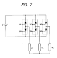
- a three-phase inverter serving as a kind of an electrical power converter incorporated in, for example, a large-capacity UPS, a battery energy storage system, or the like is adapted to perform the conversion of a dc voltage supplied from a dc power supply E, such as a solar battery and a fuel cell, into an ac voltage and to supply electric power to loads UL, VL, and WL, as shown in FIG. 7.
- a dc power supply E such as a solar battery and a fuel cell
- the three-phase inverter has a structure inwhich paired switching elements, which are arranged in an up/down direction, as viewed in this figure, and which correspond to each of a U-phase, a V-phase and a W-phase, for examples, GTO (Gate Turn-Off thyristor) elements UP, UN, VP, VN, WP, WN are connected in a bridge configuration.
- GTO Gate Turn-Off thyristor
- This inverter apparatus is adapted so that the paired GTO elements corresponding to each of the phases are alternately turned on and off, that is, a group of the GTO elements UP, VP, WP, which are shown at upper positions in the figure and correspond to a positive electrode, and a group of the GTO elements UN, VN, WN, which are shown at lower positions in the figure and correspond to a negative electrode, are alternately turned on and off. Consequently, a dc voltage supplied from the dc power supply E is converted into an ac voltage thereby to supply ac power to the loads UL, VL, and WL, as shown in FIG. 7.
- a sinusoidal waveform control signal is converted into a pulse gate signal by using a triangular waveform carrier signal. Then, each of the GTO elements UP, UN, VP, VN, WP, and WN is turned on by being applied with a forward bias voltage through the use of the gate driver. Alternatively, each of the GTO elements UP, UN, VP, VN, WP, and WN is turned off by being applied with a reverse bias voltage through the use of the gate signal.
- On/off control of these GTO elements UP, UN, VP, VN, WP, and WN is performed so that in a case where the GTO elements UP, VP, WP shown at the upper positions are in an on-state, among the paired GTO elements, and where the GTO elements UN, VN, WN shown at the lower positions are in an off-state, when the GTO elements UN, VN, WN shown at the lower positions are turned on, the GTO elements UP, VP, WP shown at the upper positions are turned off before the GTO elements UN, VN, WN turn on.
- a dead time in which the GTO elements UP, VP, WP, UN, VN, WN of both of the group shown at the upper positions and that shown at the lower positions are simultaneously brought into a turned-off state, is provided to turn on the GTO elements UN, VN, WN shown at the lower positions after a predetermined interval elapses after the GTO elements UP, VP, WP shown at the upper positions turn off. Consequently, both of the group of the GTO elements UP, VP, WP shown at the upper positions and that of the GTO elements UN, VN, WN shown at the lower positions are prevented from simultaneously being put into a turned-on state. Thus, an occurrence of a dc shortcircuit is prevented (see, for example, Patent Document 1).
- the apparatus similarly has slight stray capacitances C 7 to C 10 formed between a gate drive circuit A and each main circuit wire and between the gate drive circuit A and the earth.
- the aforementioned variation in the midpoint potential results in variation in the potential of the gate drive circuit. Consequently, a disturbance current is given to a gate current.
- the GTO element has a thyristor structure (pnpn-structure).
- pnpn-structure thyristor structure
- the turn-on gain thereof is large, while the turn-off gain thereof is extremely small. Consequently, the turn-on of the GTO element takes several tens of microseconds. Additionally, during that, a large drawing current is necessary for the turn-off. In a case where the gate drawing current in that time becomes unstable due to the disturbance current as described above, the GTO element fails to turn off, and comes to be unable to turn off. In the worst case, there is the possibility of damaging the GTO element.
- the aforementioned phenomenon occurs in a case where after the GTO element corresponding to one of the phases and to one of the electrodes turns off, a turn-on command signal for turning on the GTO element corresponding to one of the other phases and to the opposite electrode (in a case where the GTO element corresponding to the one of the phases and to the one of the electrodes is the GTO element UP, the GTO element corresponding to the one of the other phases and to the opposite electrode is the GTO element VN or WN). Occurrence of the simultaneous switching of this GTO element corresponding to the other phase causes a problem that the gate drawing current becomes unstable.
- An object of the invention is to provide an inverter apparatus enabled to eliminate variation in potential-to-the-ground of the GTO element that corresponds to one of the phases and is performing a turn-off operation, which variation is caused by the switching operation of this GTO element corresponding to the other phase, and also enabled to stabilize the gate drawing current by surely achieving the turn-off of the GTO element.
- an inverter apparatus having a three-phase inverter configured to include paired switching elements connected in a bridge configuration and to convert a power supply voltage, which is supplied from a dc power supply, by the switching elements into an ac voltage.
- This inverter apparatus features that an inverter control portion has a simultaneous switching prevention function of delaying a turn-on operation of each of the switching elements, which correspond to phases other than a phase corresponding to an optional one of the switching elements and also correspond to an electrode opposite to an electrode corresponding to the another one of the switching elements, by a predetermined time in a case where a turn-on command signal for turning on each of the switching elements, which correspond to the other phases, is generated within a predetermined time period after the turn-off of the optional one of the switching elements.
- the inverter apparatus may feature that an inverter control portion has a simultaneous switching prevention function of delaying a turn-off operation of each of the switching elements, which correspond to phases other than a phase corresponding to an optional one of the switching elements and also correspond to an electrode opposite to an electrode corresponding to the optional one of the switching elements, by a predetermined time in a case where a turn-off command signal for turning off each of the switching elements, which correspond to the other phases, is generated within a predetermined time period since turn-on of the optional one of the switching elements.
- the inverter apparatus may feature that an inverter control portion has a simultaneous switching prevention function of delaying a turn-on operation of each of the switching elements, which correspond to phases other than a phase corresponding to an optional one of the switching elements and also correspond to an electrode opposite to an electrode corresponding to the optional one of the switching elements, by a predetermined time in a case where a turn-on command signal for turning on each of the switching elements, which correspond to the other phases, is generated within a predetermined time period since turn-off of the optional one of the switching elements, and also delaying a turn-off operation of each of the switching elements, which correspond to phases other than a phase corresponding to an optional one of the switching elements and also correspond to an electrode opposite to an electrode corresponding to the optional one of the switching elements, by a predetermined time in a case where a turn-off command signal for turning off each of the switching elements, which correspond to the other phases, is generated within a predetermined time period since turn-on of the optional one of the switching elements.
- the apparatus has the simultaneous switching prevention function.
- a turn-on operation of each of the switching elements which correspond to phases other than a phase corresponding to an optional one of the switching elements and also correspond to an electrode opposite to an electrode corresponding to the optional one of the switching elements, is delayed by a predetermined time in a case where a turn-on command signal for turning on each of the switching elements, which correspond to the other phases, is generated within a predetermined time period since the turn-off of the optional one of the switching elements. Consequently, the simultaneous switching of the switching elements corresponding to the other phases can be prevented.
- the variation in potential-to-the-ground of the GTO element can be prevented from occurring during a turn-off operation thereof.
- the stabilization of the gate drawing current can be achieved by surely turning off the GTO elements.
- the Si-GTO element not only the Si-GTO element but the SiC-GTO element, which is able to operate at a higher temperature and a higher voltage than the Si-GTO element, can be used as the switching element.
- a wide-gap semiconductor such as diamond and GaN, can be used as the switching element.
- the apparatus has the simultaneous switching prevention function.
- a turn-on or turn-off operation of each of the switching elements which correspond to phases other than a phase corresponding to an optional one of the switching elements and also correspond to an electrode opposite to an electrode corresponding to the optional one of the switching elements, is delayed by a predetermined time in a case where a turn-on or turn-off command signal for turning off each of the switching elements, which correspond to the other phases, is generated within a predetermined time period since the turn-off or the turn-on of the optional one of the switching elements. Consequently, the simultaneous switching of the switching elements corresponding to the other phases can be prevented.
- the variation in potential-to-the-ground of the GTO element can be prevented from occurring during a turn-off operation thereof.
- the stabilization of the gate drawing current can be achieved by surely turning off the GTO elements.
- a high-quality inverter apparatus can be provided without causing a dc shortcircuit and a damage of the element.
- the simultaneous switching prevention function can be realized by either hardware, such as a simultaneous switching prevention circuit including a simultaneous switching prevention logic circuit, a predetermined-post-turning-off-time generating circuit, which is adapted to generate a predetermined post-turning-off time that elapses after turn-off of the optional one of the switching elements, and/or a predetermined-post-turning-on-time generating circuit which is adapted to generate a predetermined post-turning-on time that elapses after turn-on of the optional one of the switching elements, or software installed in the inverter control portion.
- a simultaneous switching prevention circuit including a simultaneous switching prevention logic circuit, a predetermined-post-turning-off-time generating circuit, which is adapted to generate a predetermined post-turning-off time that elapses after turn-off of the optional one of the switching elements, and/or a predetermined-post-turning-on-time generating circuit which is adapted to generate a predetermined post-turning-on time that e
- reference numeral 11 designates an inverter apparatus
- reference numeral 12 denotes a switching element (a Si-GTO element)
- reference numeral 13 designates a dc power supply
- reference numeral 14 denotes a three-phase inverter
- reference numeral 15 designates an inverter control circuit
- reference numeral 16 denotes a PWM pulse generating circuit
- reference numeral 17 designates a simultaneous switching prevention circuit
- reference numeral 21 denotes a inverter apparatus
- reference numeral 22 denotes a switching element (a SiC-GTO element)
- reference numeral 24 designates a three-phase inverter.
- FIG. 1 exemplifies an inverter apparatus 11 using Si-GTO elements 12 as the embodiment.
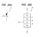
- FIG. 2 (a) shows the Si-GTO 12.
- FIG. 2(b) shows the internal structure of the Si-GTO 12.
- the Si-GTO element 12 has a pnpn structure obtained by bonding p-type semiconductor regions PE and PB and n-type semiconductor regions NB and NE and having junctions Jl, J2, and J3, each of which are provided between the associated bonded regions.
- An anode A is drawn from the p-type semiconductor region P E .
- a cathode K is drawn from the n-type semiconductor region N E .
- Agate G is drawn from the p-type semiconductor region P B .
- the Si-GTO element 12 in an on-state can be turned off by letting a gate current flow in a direction opposite to a direction of the current flowing at the turn-on thereof. That is, when a forward bias voltage is applied between the gate G and the anode A in a state, in which a positive voltage is applied to the anode A and in which a negative voltage is applied to the cathode K and this voltage is blocked by the junction J2, so that the voltage at the gate G is positive with respect to the voltage at the cathode K, holes, the number of which depends upon the magnitude of the gate current, are moved from the gate G to the semiconductor region P B .
- the Si-GTO element in an on-state cannot maintain the on-state and is put into an off-state in a case where a part of the holes transported from the semiconductor region P E to the semiconductor region P B is drawn from the gate G by applying a reverse bias voltage between the gate G and the anode A so that the voltage at the gate G is negative with respect to the voltage at the cathode K (the voltage at the cathode K is positive with respect to the voltage at the gate G), and that electros, the number of which depends upon the magnitude of the gate current, flow into the cathode K from the semiconductor region N E , and where a total of the current amplification factors of the PNP transistor portion and the NPN transistor portion is equal to or less than 1.
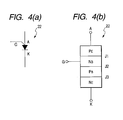
- FIG. 4(a) shows the SiC-GTO 22.
- FIG. 4 (b) shows the internal structure of the SiC-GTO 22.
- the SiC-GTO element 22 has a pnpn structure obtained by bonding p-type semiconductor regions PE and PB and n-type semiconductor regions NB and NE and having junctions J1, J2, and J3, each of which are provided between the associated bonded regions.
- An anode A is drawn from the p-type semiconductor region P E .
- a cathode K is drawn from the n-type semiconductor region N E .
- a gate G is drawn from the n-type semiconductor region N B .
- the SiC-GTO element 22 has a basic structure nearly similar to the aforementioned Si-GTO element 12, and differs from the Si-GTO element 12 in that the base part of the PNP transistor portion of the SiC-GTO element is the gate G . Therefore, a turn-on operation and a turn-off operation is performed in the SiC-GTO element 22 by applying a forwardbias voltage or a reverse bias voltage between the anode A and the gate G .
- holes the number of which depends upon the magnitude of each of the gate current and the current amplification factor of the PNP transistor portion, are transported from the semiconductor region P E to the semiconductor region P B .
- the holes transported to the semiconductor region P B serve like the base current of the NPN transistor portion.
- electrons the number of which depends upon the magnitude of each of the number of holes and the current amplification factor of the PNP transistor portion, are transported from the semiconductor region N E to the semiconductor region N B .
- the SiC-GTO element in an on-state cannot maintain the on-state and is put into an off-state in a case where a part of the electrons transported from the semiconductor region N E to the semiconductor region N B is drawn from the gate G by applying a reverse bias voltage between the gate G and the anode A so that the voltage at the gate G is positive with respect to the voltage at the anode A , and where a total of the current amplification factors of the PNP transistor portion and the NPN transistor portion is equal to or less than 1.
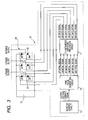
- the Si-GTO element 12 and the SiC-GTO element 22 are designated in common as the GTO elements UP, UN, VP, VN, WP, and WN, as illustrated in FIGS. 1 and 3.
- each of the embodiments which are the inverter apparatuses 11 and 21, is configured to include paired GTO elements UP, UN, VP, VN, WP, and WN, which are arranged in an up/down direction, as viewed in these figures, and which correspond to each of a U-phase, a V-phase and a W-phase and are connected in a full bridge configuration, a three-phase inverter 14 or 24 adapted to convert a power supply voltage supplied from the dc power supply 13 into an ac voltage by using the GTO elements UP, UN, VP, VN, WP, and WN, an inverter control circuit 15 adapted to generate and output the output voltage command signals Uref, Vref, and Wref (see FIG.
- an inverter control portion includes the inverter control circuit 15, the PWM pulse generating circuit 16, and the simultaneous switching prevention circuit 17.
- the inverter control circuit 15, the PWMpulse generating circuit 16, and the simultaneous switching prevention circuit 17, which generate gate signals for the GTO elements UP, UN, VP, VN, WP, and WN to drive the three-phase inverter 11 or 21, are described in detail.
- the inverter control circuit 15 is adapted to generate sinusoidal waveform output voltage command signals Uref, Vref, and Wref, which correspond to the phases, respectively, and differ from one another in phase by predetermined amounts, as illustrated in FIG. 5.
- the PWM pulse generating circuit 16 is adapted to generate the UP, UN, VP, VN, WP, and WN initial signals (see FIGS. 1 and 3), which are drive signals to cause the GTO elements UP, UN, VP, VN, WP, andWNtoperformon/offoperations, by performing PWMmodulation on the output voltage command signals Uref, Vref, and Wref outputted from the inverter control circuit 15, according to triangular waveform carrier signals K.
- the simultaneous switching prevention circuit 17 includes post-turning-off ⁇ t 1 generating circuits 18 UP , 18 UN , 18 VP , 18 VN , 18 WP , and 18 WN , post-turning-on ⁇ t 2 generating circuits 19 UP , 19 UN , 19 VP , 19 VN , 19 WP , and 19 WN , simultaneous switching preventing logic circuits 20 UP , 20 UN , 20 VP , 20 VN , 20 WP , and 20 WN' and dead time generating circuits 23 U , 23 V , and 23 W .
- the post-turning-off ⁇ t 1 generating circuits 18 UP , 18 UN , 18 VP , 18 VN , 18 WP , and 18 WN are adapted to generate a predetermined time ⁇ t 1 after the turn-off of the GTO elements UP, UN, VP, VN, WP, and WN.
- the post-turning-on ⁇ t 2 generating circuits 19 UP , 19 UN , 19 VP , 19 VN , 19 WP , and 19 WN are adapted to generate a predetermined time ⁇ t 2 after the turn-off of the GTO elements UP, UN, VP, VN, WP, and WN.
- the simultaneous switching preventing logic circuits 20 UP , 20 UN , 20 VP , 20 VN , 20 WP , and 20 WN are adapted to determine according to each of the UP, UN, VP, VN, WP, and WN initial signals, which are outputted from the PWM pulse generating circuit 16, and the signals outputted from the post-turning-off ⁇ t 1 generating circuits 18 UP , 18 UN , 18 VP , 18 VN , 18 WP , and 18 WN and the post-turning-on ⁇ t 2 generating circuits 19 UP , 19 UN , 19 VP , 19 VN , 19 WP , and 19 WN whether the turn-on operation or the turn-off operation of each of the GTO elements UP, UN, VP, VN, WP, and WN is delayed.
- the dead time generating circuits 23 U , 23 V , and 23 W are adapted to generate a dead time according to an output of each of the simultaneous switching preventing logic circuits 20 UP , 20 UN , 20 VP , 20 VN , 20 WP , and 20 WN .
- This simultaneous switching prevention circuit 17 is adapted to delay a turn-on operation of each of the GTO elements VN and WN, which correspond to phases other than a phase corresponding to, for example, the GTO element UP and also correspond to an electrode opposite to an electrode corresponding to the GTO element UP, by a predetermined time in a case where a turn-on command signal for turning on each of the GTO elements VN and WN, which correspond to the other phases, is generated within a predetermined time period ⁇ t 1 since the turn-off of the GTO element UP.
- the simultaneous switchingprevention circuit 17 is adapted to delay a turn-off operation of each of the GTO elements VN and WN, which correspond to phases other than a phase corresponding to an optional one of the GTO elements and also correspond to an electrode opposite to an electrode corresponding to the optional one of the GTO elements, by a predetermined time in a case where a turn-off command signal for turning off each of the GTO elements, which correspond to the other phases, is generated within a predetermined time period ⁇ t 2 since the turn-on of the optional one of the GTO elements.
- the inverter control circuit 15 is adapted to generate and output the sinusoidal waveform output voltage command signals Uref, Vref, and Wref, which correspond to the phases, respectively, and differ from one another in phase by predetermined amounts, as illustrated in FIG. 5, to cause the three-phase GTO elements UP, UN, VP, VN, WP, and WN to turn on or off with predetermined timing.
- the output voltage command signals Uref, Vref, andWref outputted from this inverter control circuit 15 are PWM-modulated at the PWM pulse generating circuit 16 using the triangular waveform carrier signals K.
- the UP, UN, VP, VN, WP, and WN initial signals which are used for causing the GTO elements UP, UN, VP, VN, WP, and WN to perform on/off operations, are generated and outputted.
- variation in potential occurs due to the stray capacitances C 7 to C 10 (see FIG. 8) in the dead time, in which the GTO elements of both the group shown at the upper positions and that shown at the lower positions are simultaneously in a turned-off state. Consequently, the gate drawing current becomes unstable.
- the simultaneous switching prevention circuit 17 is configured so that the dead time generating circuits 23 U , 23 V , and 23 W delay a turn-on operation of each of the GTO elements VN and WN, which correspond to phases other than a phase corresponding to one of the GTO elements and also correspond to an electrode opposite to an electrode corresponding to the one of the GTO elements, by a predetermined time according to an output of each of the post-turning-off ⁇ t 1 generating circuits 18 UP , 18 UN , 18 VP , 18 VN , 18 WP , and 18 WN , the post-turning-on ⁇ t 2 generating circuits 19 UP , 19 UN , 19 VP , 19 VN , 19 WP , and 19 WN , and the simultaneous switching preventing logic circuits 20 UP , 20 UN , 20 VP , 20 VN , 20 WP , and 20 WN in a case where a turn-on command signal for turning on each of the GTO elements VN and WN
- the GTO elements can be caused to perform on/off operations in a condition in which the aforementioned drawbacks due to the stray capacitances C 7 to C 10 are eliminated.
- All of the PWM pulse generating circuit 16 and the simultaneous switching prevention circuit 17 may be implemented by software as a PWMpulse generating circuit with a simultaneous switching prevention function.
Landscapes
- Engineering & Computer Science (AREA)
- Power Engineering (AREA)
- Inverter Devices (AREA)
Abstract
Description
- The present invention relates to an inverter apparatus enabled to prevent a simultaneous switching operation of switching elements, which are used and constitute a three-phase inverter incorporated in, for example, a large-capacity UPS, a battery energy storage system, or the like, from occurring during each of the switching elements performs an on/off operation.
- A three-phase inverter serving as a kind of an electrical power converter incorporated in, for example, a large-capacity UPS, a battery energy storage system, or the like is adapted to perform the conversion of a dc voltage supplied from a dc power supply E, such as a solar battery and a fuel cell, into an ac voltage and to supply electric power to loads UL, VL, and WL, as shown in FIG. 7. The three-phase inverter has a structure inwhich paired switching elements, which are arranged in an up/down direction, as viewed in this figure, and which correspond to each of a U-phase, a V-phase and a W-phase, for examples, GTO (Gate Turn-Off thyristor) elements UP, UN, VP, VN, WP, WN are connected in a bridge configuration.
- This inverter apparatus is adapted so that the paired GTO elements corresponding to each of the phases are alternately turned on and off, that is, a group of the GTO elements UP, VP, WP, which are shown at upper positions in the figure and correspond to a positive electrode, and a group of the GTO elements UN, VN, WN, which are shown at lower positions in the figure and correspond to a negative electrode, are alternately turned on and off. Consequently, a dc voltage supplied from the dc power supply E is converted into an ac voltage thereby to supply ac power to the loads UL, VL, and WL, as shown in FIG. 7.
- A sinusoidal waveform control signal is converted into a pulse gate signal by using a triangular waveform carrier signal. Then, each of the GTO elements UP, UN, VP, VN, WP, and WN is turned on by being applied with a forward bias voltage through the use of the gate driver. Alternatively, each of the GTO elements UP, UN, VP, VN, WP, and WN is turned off by being applied with a reverse bias voltage through the use of the gate signal.
- On/off control of these GTO elements UP, UN, VP, VN, WP, and WN is performed so that in a case where the GTO elements UP, VP, WP shown at the upper positions are in an on-state, among the paired GTO elements, and where the GTO elements UN, VN, WN shown at the lower positions are in an off-state, when the GTO elements UN, VN, WN shown at the lower positions are turned on, the GTO elements UP, VP, WP shown at the upper positions are turned off before the GTO elements UN, VN, WN turn on.
- A dead time, in which the GTO elements UP, VP, WP, UN, VN, WN of both of the group shown at the upper positions and that shown at the lower positions are simultaneously brought into a turned-off state, is provided to turn on the GTO elements UN, VN, WN shown at the lower positions after a predetermined interval elapses after the GTO elements UP, VP, WP shown at the upper positions turn off. Consequently, both of the group of the GTO elements UP, VP, WP shown at the upper positions and that of the GTO elements UN, VN, WN shown at the lower positions are prevented from simultaneously being put into a turned-on state. Thus, an occurrence of a dc shortcircuit is prevented (see, for example, Patent Document 1).
- Meanwhile, generally, as shown in FIG. 8, slight stray capacitances C1 to C6 are formed between output wires and between the output wire and the earth (or a casing) in the aforementioned inverter apparatus. Therefore, the presence of a dead time, in which the GTO elements of both the group shown at the upper positions and that shown at the lower positions are simultaneously in a turned-off state, as described above, results in discharge of electric charges stored in the stray capacitances to thereby vary the midpoint potential of the GTO elements corresponding to a phase with respect to that of the GTO elements corresponding to another phase. Incidentally, the apparatus similarly has slight stray capacitances C7 to C10 formed between a gate drive circuit A and each main circuit wire and between the gate drive circuit A and the earth. Thus, the aforementioned variation in the midpoint potential results in variation in the potential of the gate drive circuit. Consequently, a disturbance current is given to a gate current.
- Meanwhile, the GTO element has a thyristor structure (pnpn-structure). Thus, the turn-on gain thereof is large, while the turn-off gain thereof is extremely small. Consequently, the turn-on of the GTO element takes several tens of microseconds. Additionally, during that, a large drawing current is necessary for the turn-off. In a case where the gate drawing current in that time becomes unstable due to the disturbance current as described above, the GTO element fails to turn off, and comes to be unable to turn off. In the worst case, there is the possibility of damaging the GTO element.
- The aforementioned phenomenon occurs in a case where after the GTO element corresponding to one of the phases and to one of the electrodes turns off, a turn-on command signal for turning on the GTO element corresponding to one of the other phases and to the opposite electrode (in a case where the GTO element corresponding to the one of the phases and to the one of the electrodes is the GTO element UP, the GTO element corresponding to the one of the other phases and to the opposite electrode is the GTO element VN or WN). Occurrence of the simultaneous switching of this GTO element corresponding to the other phase causes a problem that the gate drawing current becomes unstable.
- Accordingly, the invention is proposed in view of the aforementioned problem. An object of the invention is to provide an inverter apparatus enabled to eliminate variation in potential-to-the-ground of the GTO element that corresponds to one of the phases and is performing a turn-off operation, which variation is caused by the switching operation of this GTO element corresponding to the other phase, and also enabled to stabilize the gate drawing current by surely achieving the turn-off of the GTO element.
- As technical means for attaining the foregoing object, according to the invention, there is provided an inverter apparatus having a three-phase inverter configured to include paired switching elements connected in a bridge configuration and to convert a power supply voltage, which is supplied from a dc power supply, by the switching elements into an ac voltage. This inverter apparatus features that an inverter control portion has a simultaneous switching prevention function of delaying a turn-on operation of each of the switching elements, which correspond to phases other than a phase corresponding to an optional one of the switching elements and also correspond to an electrode opposite to an electrode corresponding to the another one of the switching elements, by a predetermined time in a case where a turn-on command signal for turning on each of the switching elements, which correspond to the other phases, is generated within a predetermined time period after the turn-off of the optional one of the switching elements.
- Alternatively, the inverter apparatus according to the invention may feature that an inverter control portion has a simultaneous switching prevention function of delaying a turn-off operation of each of the switching elements, which correspond to phases other than a phase corresponding to an optional one of the switching elements and also correspond to an electrode opposite to an electrode corresponding to the optional one of the switching elements, by a predetermined time in a case where a turn-off command signal for turning off each of the switching elements, which correspond to the other phases, is generated within a predetermined time period since turn-on of the optional one of the switching elements.
- Alternatively, the inverter apparatus according to the invention may feature that an inverter control portion has a simultaneous switching prevention function of delaying a turn-on operation of each of the switching elements, which correspond to phases other than a phase corresponding to an optional one of the switching elements and also correspond to an electrode opposite to an electrode corresponding to the optional one of the switching elements, by a predetermined time in a case where a turn-on command signal for turning on each of the switching elements, which correspond to the other phases, is generated within a predetermined time period since turn-off of the optional one of the switching elements, and also delaying a turn-off operation of each of the switching elements, which correspond to phases other than a phase corresponding to an optional one of the switching elements and also correspond to an electrode opposite to an electrode corresponding to the optional one of the switching elements, by a predetermined time in a case where a turn-off command signal for turning off each of the switching elements, which correspond to the other phases, is generated within a predetermined time period since turn-on of the optional one of the switching elements.
- According to the invention, the apparatus has the simultaneous switching prevention function. Thus, for example, a turn-on operation of each of the switching elements, which correspond to phases other than a phase corresponding to an optional one of the switching elements and also correspond to an electrode opposite to an electrode corresponding to the optional one of the switching elements, is delayed by a predetermined time in a case where a turn-on command signal for turning on each of the switching elements, which correspond to the other phases, is generated within a predetermined time period since the turn-off of the optional one of the switching elements. Consequently, the simultaneous switching of the switching elements corresponding to the other phases can be prevented. Thus, the variation in potential-to-the-ground of the GTO element can be prevented from occurring during a turn-off operation thereof. Also, the stabilization of the gate drawing current can be achieved by surely turning off the GTO elements.
- Incidentally, according to the invention, not only the Si-GTO element but the SiC-GTO element, which is able to operate at a higher temperature and a higher voltage than the Si-GTO element, can be used as the switching element. Alternatively, a wide-gap semiconductor, such as diamond and GaN, can be used as the switching element.
- According to the invention, the apparatus has the simultaneous switching prevention function. Thus, a turn-on or turn-off operation of each of the switching elements, which correspond to phases other than a phase corresponding to an optional one of the switching elements and also correspond to an electrode opposite to an electrode corresponding to the optional one of the switching elements, is delayed by a predetermined time in a case where a turn-on or turn-off command signal for turning off each of the switching elements, which correspond to the other phases, is generated within a predetermined time period since the turn-off or the turn-on of the optional one of the switching elements. Consequently, the simultaneous switching of the switching elements corresponding to the other phases can be prevented. Thus, for instance, the variation in potential-to-the-ground of the GTO element can be prevented from occurring during a turn-off operation thereof. The stabilization of the gate drawing current can be achieved by surely turning off the GTO elements. A high-quality inverter apparatus can be provided without causing a dc shortcircuit and a damage of the element.
- Also, the simultaneous switching prevention function can be realized by either hardware, such as a simultaneous switching prevention circuit including a simultaneous switching prevention logic circuit, a predetermined-post-turning-off-time generating circuit, which is adapted to generate a predetermined post-turning-off time that elapses after turn-off of the optional one of the switching elements, and/or a predetermined-post-turning-on-time generating circuit which is adapted to generate a predetermined post-turning-on time that elapses after turn-on of the optional one of the switching elements, or software installed in the inverter control portion.
-
- FIG. 1 is a circuit diagram illustrating an embodiment of the invention, which is an inverter apparatus having a three-phase inverter that includes Si-GTO elements.
- FIG. 2 (a) is a diagram illustrating a Si-GTO element, and FIG. 2 (b) is a diagram illustrating the internal structure of the Si-GTO element.
- FIG. 3 is a circuit diagram illustrating another embodiment of the invention, which is an inverter apparatus having a three-phase inverter that includes SiC-GTO elements.
- FIG. 4(a) is a diagram illustrating a SiC-GTO element, and FIG. 4 (b) is a diagram illustrating the internal structure of this SiC-GTO element.
- FIG. 5 is a waveform chart illustrating an output voltage command signal, a carrier signal, and a gate initial signal.
- FIG. 6 is a block diagram illustrating the internal structure of a simultaneous switching prevention circuit shown in FIGS. 1 and 3.
- FIG. 7 is a circuit diagram illustrating an example of a three-phase inverter.
- FIG. 8 is an explanatory diagram illustrating the generation of stray capacitances in a three-phase inverter.
- Incidentally, in the drawings,
reference numeral 11 designates an inverter apparatus,reference numeral 12 denotes a switching element (a Si-GTO element),reference numeral 13 designates a dc power supply,reference numeral 14 denotes a three-phase inverter,reference numeral 15 designates an inverter control circuit,reference numeral 16 denotes a PWM pulse generating circuit,reference numeral 17 designates a simultaneous switching prevention circuit,reference numeral 21 denotes a inverter apparatus,reference numeral 22 denotes a switching element (a SiC-GTO element), andreference numeral 24 designates a three-phase inverter. - Hereinafter, an embodiment of an inverter apparatus according to the invention is described in detail. Incidentally, the following description of the embodiment describes a case where Si-
GTO elements 12 are used as the switching elements (see FIGS. 1 and 2), and a case where SiC-GTO elements 22, which can operate at a higher temperature and a higher voltage than the Si-GTO elements 12 (see FIGS. 3 and 4). - FIG. 1 exemplifies an
inverter apparatus 11 using Si-GTO elements 12 as the embodiment. FIG. 2 (a) shows the Si-GTO 12. FIG. 2(b) shows the internal structure of the Si-GTO 12. As shown in FIGS. 2 (a) and 2 (b), the Si-GTO element 12 has a pnpn structure obtained by bonding p-type semiconductor regions PE and PB and n-type semiconductor regions NB and NE and having junctions Jl, J2, and J3, each of which are provided between the associated bonded regions. An anode A is drawn from the p-type semiconductor region PE. A cathode K is drawn from the n-type semiconductor region NE. Agate G is drawn from the p-type semiconductor region PB. - Generally, the Si-
GTO element 12 in an on-state can be turned off by letting a gate current flow in a direction opposite to a direction of the current flowing at the turn-on thereof. That is, when a forward bias voltage is applied between the gate G and the anode A in a state, in which a positive voltage is applied to the anode A and in which a negative voltage is applied to the cathode K and this voltage is blocked by the junction J2, so that the voltage at the gate G is positive with respect to the voltage at the cathode K, holes, the number of which depends upon the magnitude of the gate current, are moved from the gate G to the semiconductor region PB. Similarly to a state in which a base current is supplied to an NPN transistor portion, electrons, the number of which depends upon the magnitude of each of the gate current and the current amplification factor of the NPN transistor portion, are transported from the semiconductor region NE to the semiconductor region NB. The electrons transported to the semiconductor region NB serve like the base current of a PNP transistor portion. Also, holes, the number of which depends upon the magnitude of each of the number of electrons and the current amplification factor of the PNP transistor portion, are transported from the semiconductor region PE to the semiconductor region PB. In this way, what are called carriers, such as holes and electrons, pass through the junction J2 by applying a forward bias voltage between the gate of the NPN transistor portion of the Si-GTO element, which that is in an off-state. Thus, the Si-GTO element cannot maintain the off-state, so that electric current starts flowing, and that the Si-GTO element turns on. - Meanwhile, the Si-GTO element in an on-state cannot maintain the on-state and is put into an off-state in a case where a part of the holes transported from the semiconductor region PE to the semiconductor region PB is drawn from the gate G by applying a reverse bias voltage between the gate G and the anode A so that the voltage at the gate G is negative with respect to the voltage at the cathode K (the voltage at the cathode K is positive with respect to the voltage at the gate G), and that electros, the number of which depends upon the magnitude of the gate current, flow into the cathode K from the semiconductor region NE, and where a total of the current amplification factors of the PNP transistor portion and the NPN transistor portion is equal to or less than 1.
- Referring next to FIG. 3, there is exemplified an
inverter apparatus 21 employing SiC-GTO elements 22, which can operate at a higher temperature and a higher voltage than the Si-GTO elements 12, as an embodiment. FIG. 4(a) shows the SiC-GTO 22. FIG. 4 (b) shows the internal structure of the SiC-GTO 22. As shown in FIGS. 4(a) and 4(b), the SiC-GTO element 22 has a pnpn structure obtained by bonding p-type semiconductor regions PE and PB and n-type semiconductor regions NB and NE and having junctions J1, J2, and J3, each of which are provided between the associated bonded regions. An anode A is drawn from the p-type semiconductor region PE. A cathode K is drawn from the n-type semiconductor region NE. A gate G is drawn from the n-type semiconductor region NB. - The SiC-
GTO element 22 has a basic structure nearly similar to the aforementioned Si-GTO element 12, and differs from the Si-GTO element 12 in that the base part of the PNP transistor portion of the SiC-GTO element is the gate G. Therefore, a turn-on operation and a turn-off operation is performed in the SiC-GTO element 22 by applying a forwardbias voltage or a reverse bias voltage between the anode A and the gate G. - Practically, when a forward bias voltage is applied between the gate G and the anode A in a state, in which a positive voltage is applied to the anode A and in which a negative voltage is applied to the cathode K and this voltage is blocked by the junction J2, so that the voltage at the gate G is negative with respect to the voltage at the anode A (the voltage at the anode A is positive with respect to the voltage at the gate G), electrons, the number of which depends upon the magnitude of the gate current, flow into the semiconductor region NB from the gate G . Similarly to a state in which abase current is supplied to the PNP transistor portion, holes, the number of which depends upon the magnitude of each of the gate current and the current amplification factor of the PNP transistor portion, are transported from the semiconductor region PE to the semiconductor region PB. The holes transported to the semiconductor region PB serve like the base current of the NPN transistor portion. Also, electrons, the number of which depends upon the magnitude of each of the number of holes and the current amplification factor of the PNP transistor portion, are transported from the semiconductor region NE to the semiconductor region NB. In this manner, what are called carriers, such as holes and electrons, pass through the junction J2 by applying a forward bias voltage between the gate of the NPN transistor portion of the SiC-
GTO element 22, which that is in an off-state. Thus, the SiC-GTO element 22 cannot maintain the off-state, so that electric current starts flowing, and that the SiC-GTO element 22 turns on. - Meanwhile, the SiC-GTO element in an on-state cannot maintain the on-state and is put into an off-state in a case where a part of the electrons transported from the semiconductor region NE to the semiconductor region NB is drawn from the gate G by applying a reverse bias voltage between the gate G and the anode A so that the voltage at the gate G is positive with respect to the voltage at the anode A, and where a total of the current amplification factors of the PNP transistor portion and the NPN transistor portion is equal to or less than 1.
- Hereinafter, in view of redundant descriptions of the Si-
GTO elements 12 and the SiC-GTO elements 22, the Si-GTO element 12 and the SiC-GTO element 22 are designated in common as the GTO elements UP, UN, VP, VN, WP, and WN, as illustrated in FIGS. 1 and 3. - As shown in FIGS. 1 and 3, each of the embodiments, which are the inverter apparatuses 11 and 21, is configured to include paired GTO elements UP, UN, VP, VN, WP, and WN, which are arranged in an up/down direction, as viewed in these figures, and which correspond to each of a U-phase, a V-phase and a W-phase and are connected in a full bridge configuration, a three-phase inverter 14 or 24 adapted to convert a power supply voltage supplied from the dc power supply 13 into an ac voltage by using the GTO elements UP, UN, VP, VN, WP, and WN, an inverter control circuit 15 adapted to generate and output the output voltage command signals Uref, Vref, and Wref (see FIG. 5) to change the value of an output voltage of the inverter 14 or 24 to a predetermined value, a PWM pulse generating circuit 16 adapted to generate and output drive signals, which cause the GTO elements UP, UN, VP, VN, WP, and WN to perform on/off operations, by performing PWM-modulation on the output voltage command signals Uref, Vref, and Wref, and a simultaneous switching prevention circuit 17 adapted to generate and output a gate signal by delaying the drive signal, which is outputted from the PWM pulse generating circuit 16, by a predetermined time according to conditions that will be described later. Incidentally, an inverter control portion includes the
inverter control circuit 15, the PWMpulse generating circuit 16, and the simultaneousswitching prevention circuit 17. - Hereinafter, the
inverter control circuit 15, thePWMpulse generating circuit 16, and the simultaneousswitching prevention circuit 17, which generate gate signals for the GTO elements UP, UN, VP, VN, WP, and WN to drive the three-phase inverter - The
inverter control circuit 15 is adapted to generate sinusoidal waveform output voltage command signals Uref, Vref, and Wref, which correspond to the phases, respectively, and differ from one another in phase by predetermined amounts, as illustrated in FIG. 5. - The PWM
pulse generating circuit 16 is adapted to generate the UP, UN, VP, VN, WP, and WN initial signals (see FIGS. 1 and 3), which are drive signals to cause the GTO elements UP, UN, VP, VN, WP, andWNtoperformon/offoperations, by performing PWMmodulation on the output voltage command signals Uref, Vref, and Wref outputted from theinverter control circuit 15, according to triangular waveform carrier signals K. - As shown in FIG. 6, the simultaneous
switching prevention circuit 17 includes post-turning-off Δt1 generating circuits 18UP, 18UN, 18VP, 18VN, 18WP, and 18WN, post-turning-on Δt2 generating circuits 19UP, 19UN, 19VP, 19VN, 19WP, and 19WN, simultaneous switching preventing logic circuits 20UP, 20UN, 20VP, 20VN, 20WP, and 20WN' and dead time generating circuits 23U, 23V, and 23W. - The post-turning-off Δt1 generating circuits 18UP, 18UN, 18VP, 18VN, 18WP, and 18WN are adapted to generate a predetermined time Δt1 after the turn-off of the GTO elements UP, UN, VP, VN, WP, and WN. The post-turning-on Δt2 generating circuits 19UP, 19UN, 19VP, 19VN, 19WP, and 19WN are adapted to generate a predetermined time Δt2 after the turn-off of the GTO elements UP, UN, VP, VN, WP, and WN.
- The simultaneous switching preventing logic circuits 20UP, 20UN, 20VP, 20VN, 20WP, and 20WN are adapted to determine according to each of the UP, UN, VP, VN, WP, and WN initial signals, which are outputted from the PWM
pulse generating circuit 16, and the signals outputted from the post-turning-off Δt1 generating circuits 18UP, 18UN, 18VP, 18VN, 18WP, and 18WN and the post-turning-on Δt2 generating circuits 19UP, 19UN, 19VP, 19VN, 19WP, and 19WN whether the turn-on operation or the turn-off operation of each of the GTO elements UP, UN, VP, VN, WP, and WN is delayed. - The dead time generating circuits 23U, 23V, and 23W are adapted to generate a dead time according to an output of each of the simultaneous switching preventing logic circuits 20UP, 20UN, 20VP, 20VN, 20WP, and 20WN.
- This simultaneous
switching prevention circuit 17 is adapted to delay a turn-on operation of each of the GTO elements VN and WN, which correspond to phases other than a phase corresponding to, for example, the GTO element UP and also correspond to an electrode opposite to an electrode corresponding to the GTO element UP, by a predetermined time in a case where a turn-on command signal for turning on each of the GTO elements VN and WN, which correspond to the other phases, is generated within a predetermined time period Δt1 since the turn-off of the GTO element UP. Incidentally, thesimultaneous switchingprevention circuit 17 is adapted to delay a turn-off operation of each of the GTO elements VN and WN, which correspond to phases other than a phase corresponding to an optional one of the GTO elements and also correspond to an electrode opposite to an electrode corresponding to the optional one of the GTO elements, by a predetermined time in a case where a turn-off command signal for turning off each of the GTO elements, which correspond to the other phases, is generated within a predetermined time period Δt2 since the turn-on of the optional one of the GTO elements. - In this embodiment, which is the
inverter apparatus inverter control circuit 15 is adapted to generate and output the sinusoidal waveform output voltage command signals Uref, Vref, and Wref, which correspond to the phases, respectively, and differ from one another in phase by predetermined amounts, as illustrated in FIG. 5, to cause the three-phase GTO elements UP, UN, VP, VN, WP, and WN to turn on or off with predetermined timing. The output voltage command signals Uref, Vref, andWref outputted from thisinverter control circuit 15 are PWM-modulated at the PWMpulse generating circuit 16 using the triangular waveform carrier signals K. Thus, the UP, UN, VP, VN, WP, and WN initial signals, which are used for causing the GTO elements UP, UN, VP, VN, WP, and WN to perform on/off operations, are generated and outputted. - Incidentally, as illustrated in FIG. 5, the simultaneous switching of one of the GTO elements corresponding to one of the phases (for example, the GTO element UP) and the GTO elements (for instance, the GTO elements VN and WN), which correspond to the phases other than the phase corresponding to the one of the phases and to an electrode opposite to an electrode corresponding to the one of the GTO elements, occurs at intersection points P1, P2, ..., at each of which the carrier signal K intersects with two of the three-phase output voltage command signals Uref, Vref, and Wref. Thus, variation in potential occurs due to the stray capacitances C7 to C10 (see FIG. 8) in the dead time, in which the GTO elements of both the group shown at the upper positions and that shown at the lower positions are simultaneously in a turned-off state. Consequently, the gate drawing current becomes unstable.
- Thus, the simultaneous
switching prevention circuit 17 is configured so that the dead time generating circuits 23U, 23V, and 23W delay a turn-on operation of each of the GTO elements VN and WN, which correspond to phases other than a phase corresponding to one of the GTO elements and also correspond to an electrode opposite to an electrode corresponding to the one of the GTO elements, by a predetermined time according to an output of each of the post-turning-off Δt1 generating circuits 18UP, 18UN, 18VP, 18VN, 18WP, and 18WN, the post-turning-on Δt2 generating circuits 19UP, 19UN, 19VP, 19VN, 19WP, and 19WN, and the simultaneous switching preventing logic circuits 20UP, 20UN, 20VP, 20VN, 20WP, and 20WN in a case where a turn-on command signal for turning on each of the GTO elements VN and WN, which correspond to the other phases, is generated within a predetermined time period Δt1 since the turn-off of the one of the GTO elements. Occurrence of the simultaneous switching is prevented by causing the GTO elements to perform on/off operations according to the gate signals outputted from the simultaneousswitching prevention circuit 17. Thus, the GTO elements can be caused to perform on/off operations in a condition in which the aforementioned drawbacks due to the stray capacitances C7 to C10 are eliminated. - All of the PWM
pulse generating circuit 16 and the simultaneousswitching prevention circuit 17 may be implemented by software as a PWMpulse generating circuit with a simultaneous switching prevention function. - Although the specific embodiments of the invention have been described in detail with reference to the accompanying drawings, it is apparent to those skilled in the art that various changes and modifications may be made without departing from the scope and the spirit of the invention.
- FIG. 1, FIG. 3
- a
- U-PHASE OUTPUT
- b
- V-PHASE OUTPUT
- c
- W-PHASE OUTPUT
- d
- INVERTER CONTROL CIRCUIT
- e
- OUTPUT VOLTAGE COMMAND SIGNAL
- f
- PWM PULSE GENERATING CIRCUIT
- g
- UP INITIAL SIGNAL
- h
- UN INITIAL SIGNAL
- i
- VP INITIAL SIGNAL
- j
- VN INITIAL SIGNAL
- k
- WP INITIAL SIGNAL
- l
- WN INITIAL SIGNAL
- m
- SIMULTANEOUS SWITCHING PREVENTION CIRCUIT
- n
- UP GATE SIGNAL
- o
- UN GATE SIGNAL
- p
- VP GATE SIGNAL
- q
- VN GATE SIGNAL
- r
- WP GATE SIGNAL
- s
- WN GATE SIGNAL
- FIG. 5
a,b,c,d,e··· HIGH-POSSIBILITY SIMULTANEOUS-SWITCHING POINTS - FIG. 6
- a
- UP INITIAL SIGNAL
- b
- POST-TURNING-OFF Δt1 GENERATING CIRCUIT
- C
- POST-TURNING-ON Δt2 GENERATING CIRCUIT
- d
- SIMULTANEOUS SWITCHING PREVENTION LOGIC CIRCUIT
- e
- DEAD TIME GENERATING CIRCUIT
- f
- UP GATE SIGNAL
- g
- UN GATE SIGNAL
- h
- UN INITIAL SIGNAL
- i
- VP INITIAL SIGNAL
- j
- VP GATE SIGNAL
- k
- VN GATE SIGNAL
- l
- VN INITIAL SIGNAL
- m
- WP INITIAL SIGNAL
- n···
- WP GATE SIGNAL
- o···
- WN GATE SIGNAL
- p···
- WN INITIAL SIGNAL
- FIG. 8
A··· GATE DRIVE CIRCUIT
Claims (8)
- An inverter apparatus having a three-phase inverter configured to include paired switching elements connected in a bridge configuration and to convert a power supply voltage, which is supplied from a dc power supply, by said switching elements into an ac voltage, characterized in that:an inverter control portion has a simultaneous switching prevention function of delaying a turn-on operation of each of said switching elements, which correspond to phases other than a phase corresponding to an optional one of said switching elements and also correspond to an electrode opposite to an electrode corresponding to said optional one of said switching elements, by a predetermined time in a case where a turn-on command signal for turning on each of said switching elements, which correspond to the other phases, is generated within a predetermined time period since turn-off of said optional one of said switching elements.
- An inverter apparatus having a three-phase inverter configured to include paired switching elements connected in a bridge configuration and to convert a power supply voltage, which is supplied from a dc power supply, by said switching elements into an ac voltage, characterized in that:an inverter control portion has a simultaneous switching prevention function of delaying a turn-off operation of each of said switching elements, which correspond to phases other than a phase corresponding to an optional one of said switching elements and also correspond to an electrode opposite to an electrode corresponding to said optional one of said switching elements, by a predetermined time in a case where a turn-off command signal for turning off each of said switching elements, which correspond to the other phases, is generated within a predetermined time period since turn-on of said optional one of said switching elements.
- An inverter apparatus having a three-phase inverter configured to include paired switching elements connected in a bridge configuration and to convert a power supply voltage, which is supplied from a dc power supply, by said switching elements into an ac voltage, characterized in that:an inverter control portion has a simultaneous switching prevention function of delaying a turn-on operation of each of said switching elements, which correspond to phases other than a phase corresponding to an optional one of said switching elements and also correspond to an electrode opposite to an electrode corresponding to said optional one of said switching elements, by a predetermined time in a case where a turn-on command signal for turning on each of said switching elements, which correspond to the other phases, is generated within a predetermined time period since turn-off of said optional one of said switching elements, and also delaying a turn-off operation of each of said switching elements, which correspond to phases other than a phase corresponding to an optional one of said switching elements and also correspond to an electrode opposite to an electrode corresponding to said optional one of said switching elements, by a predetermined time in a case where a turn-off command signal for turning off each of said switching elements, which correspond to the other phases, is generated within a predetermined time period since turn-on of said optional one of said switching elements.
- The inverter apparatus according to one of claims 1 to 3, wherein all of the simultaneous switching prevention function is realized by software in said inverter control portion.
- The inverter apparatus according to one of claims 1 to 3, characterized in that:the simultaneous switching prevention function is achieved by a simultaneous switching prevention circuit including a predetermined-post-turning-off-time generating circuit, which is adapted to generate a predetermined time that elapses after turn-off of the optional one of said switching elements and/or a predetermined-post-turning-on-time generating circuit which is adapted to generate a predetermined time that elapses after turn-on of the optional one of said switching elements, and a simultaneous switching prevention logic circuit.
- The inverter apparatus according to one of claims 1 to 5, wherein said switching elements are Si-GTO elements.
- The inverter apparatus according to one of claims 1 to 5, wherein said switching elements are SiC-GTO elements.
- The inverter apparatus according to one of claims 1 to 5, wherein said switching elements are wide-gap semiconductors including diamond and GaN.
Applications Claiming Priority (2)
| Application Number | Priority Date | Filing Date | Title |
|---|---|---|---|
| JP2003279312A JP4328884B2 (en) | 2003-07-24 | 2003-07-24 | Inverter device |
| PCT/JP2004/010897 WO2005011096A1 (en) | 2003-07-24 | 2004-07-23 | Inverter apparatus |
Publications (2)
| Publication Number | Publication Date |
|---|---|
| EP1653598A1 true EP1653598A1 (en) | 2006-05-03 |
| EP1653598A4 EP1653598A4 (en) | 2009-06-03 |
Family
ID=34100811
Family Applications (1)
| Application Number | Title | Priority Date | Filing Date |
|---|---|---|---|
| EP04748104A Withdrawn EP1653598A4 (en) | 2003-07-24 | 2004-07-23 | Inverter apparatus |
Country Status (4)
| Country | Link |
|---|---|
| US (1) | US7570502B2 (en) |
| EP (1) | EP1653598A4 (en) |
| JP (1) | JP4328884B2 (en) |
| WO (1) | WO2005011096A1 (en) |
Families Citing this family (4)
| Publication number | Priority date | Publication date | Assignee | Title |
|---|---|---|---|---|
| EP2001385B1 (en) * | 2006-01-17 | 2016-03-23 | Endymed Medical Ltd. | Electrosurgical methods and devices employing phase-controlled radiofrequency energy |
| JP4772542B2 (en) * | 2006-03-15 | 2011-09-14 | 株式会社東芝 | Power converter |
| WO2012039094A1 (en) * | 2010-09-24 | 2012-03-29 | 富士電機株式会社 | Power conversion apparatus and method of controlling thereof |
| WO2021050912A1 (en) | 2019-09-13 | 2021-03-18 | Milwaukee Electric Tool Corporation | Power converters with wide bandgap semiconductors |
Family Cites Families (17)
| Publication number | Priority date | Publication date | Assignee | Title |
|---|---|---|---|---|
| US4447867A (en) * | 1982-01-29 | 1984-05-08 | Varo, Inc. | Multiphase inverter drive circuit with synchronized switching delay feature |
| JPS59123478A (en) * | 1982-12-28 | 1984-07-17 | Toshiba Corp | Controller for voltage type inverter |
| GB8309226D0 (en) * | 1983-04-05 | 1983-05-11 | Fairford Electronics Ltd | Start-up control method |
| GB8706275D0 (en) * | 1987-03-17 | 1987-04-23 | Rca Corp | Gate circuit |
| JPS63287371A (en) * | 1987-05-15 | 1988-11-24 | Mitsubishi Electric Corp | Interphase reactor multiplex system pwm inverter |
| EP0328941A1 (en) | 1988-02-16 | 1989-08-23 | Siemens Aktiengesellschaft | Process and device for the commutation of current between turn-off switches of a current rectifier |
| JPH01303067A (en) | 1988-05-31 | 1989-12-06 | Fuji Electric Co Ltd | Control circuit for pwm inverter |
| JPH06113559A (en) | 1992-09-25 | 1994-04-22 | Mitsubishi Heavy Ind Ltd | GTO inverter circuit |
| US5671130A (en) * | 1996-08-23 | 1997-09-23 | Allen-Bradley Company, Inc. | Method and apparatus for controlling voltage reflections using a motor controller |
| JP3580048B2 (en) | 1996-10-03 | 2004-10-20 | 富士電機システムズ株式会社 | Inverter dead time compensation circuit |
| US5912813A (en) * | 1997-10-01 | 1999-06-15 | Allen-Bradley Company, Llc | Method and apparatus for controlling reflected voltage using a motor controller |
| JP4128645B2 (en) * | 1998-01-12 | 2008-07-30 | 株式会社日立製作所 | Inverter for rotating electrical machine |
| JP2000295863A (en) | 1999-04-06 | 2000-10-20 | Mitsubishi Electric Corp | Inverter device |
| JP2002111010A (en) | 2000-09-26 | 2002-04-12 | Hitachi Ltd | Semiconductor device and converter using the same |
| JP4021151B2 (en) * | 2001-03-06 | 2007-12-12 | 株式会社東芝 | Induction heating cooker |
| US6570780B2 (en) * | 2001-05-17 | 2003-05-27 | Honda Giken Kogyo Kabushiki Kaisha | Resonant inverter control system |
| WO2005020320A1 (en) * | 2003-08-22 | 2005-03-03 | The Kansai Electric Power Co., Inc. | Semiconductor device, method for manufacturing same, and power converter using such semiconductor device |
-
2003
- 2003-07-24 JP JP2003279312A patent/JP4328884B2/en not_active Expired - Fee Related
-
2004
- 2004-07-23 US US10/565,389 patent/US7570502B2/en not_active Expired - Fee Related
- 2004-07-23 WO PCT/JP2004/010897 patent/WO2005011096A1/en not_active Ceased
- 2004-07-23 EP EP04748104A patent/EP1653598A4/en not_active Withdrawn
Also Published As
| Publication number | Publication date |
|---|---|
| JP2005045964A (en) | 2005-02-17 |
| JP4328884B2 (en) | 2009-09-09 |
| EP1653598A4 (en) | 2009-06-03 |
| US7570502B2 (en) | 2009-08-04 |
| WO2005011096A1 (en) | 2005-02-03 |
| US20060245223A1 (en) | 2006-11-02 |
Similar Documents
| Publication | Publication Date | Title |
|---|---|---|
| US11721689B2 (en) | Semiconductor device having a semiconductor channel region and a semiconductor auxiliary region | |
| EP2712085B1 (en) | Switching circuit and semiconductor module | |
| US4870555A (en) | High-efficiency DC-to-DC power supply with synchronous rectification | |
| KR101076744B1 (en) | Semiconductor switch and power converter to which the semiconductor switch is applied | |
| US5661644A (en) | Converter circuit, circuitry having at least one switching device and circuit module | |
| US10547251B1 (en) | Method for shutdown of an active neutral point clamped converter | |
| US6657874B2 (en) | Semiconductor converter circuit and circuit module | |
| US20200366186A1 (en) | Modular multilevel converter sub-module having dc fault current blocking function and method of controlling the same | |
| CN102347702A (en) | Highly efficient half-bridge dcac converter | |
| US12575168B2 (en) | RC IGBT, method of producing an RC IGBT and method of controlling a half bridge circuit | |
| AU2014297873A1 (en) | Semiconductor device and power conversion device | |
| Ren et al. | Multi-commutation loop induced over-voltage issue on non-active switches in fast switching speed three-level active neutral point clamped phase leg | |
| US7248093B2 (en) | Bipolar bootstrap top switch gate drive for half-bridge semiconductor power topologies | |
| US7570502B2 (en) | Inverter apparatus comprising switching elements | |
| US11146168B2 (en) | Snubber circuit and power conversion apparatus | |
| JPH10164854A (en) | Power converter | |
| US12191790B2 (en) | Power module with protection circuit | |
| JP3367839B2 (en) | Semiconductor device | |
| KR101280424B1 (en) | 3-phase asymmetric inverter circuit for asymmetric PWM method | |
| KR20200118932A (en) | High speed switching inverter | |
| US20230261562A1 (en) | Power conversion device and control method thereof | |
| Majumdar et al. | Active surge voltage clamped 600 A IPM for high power application | |
| JP2000166248A (en) | Power converter | |
| KR100287532B1 (en) | Active IGBT element series drive circuit and its driving method | |
| JPS62256529A (en) | Thyristor circuit |
Legal Events
| Date | Code | Title | Description |
|---|---|---|---|
| PUAI | Public reference made under article 153(3) epc to a published international application that has entered the european phase |
Free format text: ORIGINAL CODE: 0009012 |
|
| 17P | Request for examination filed |
Effective date: 20060124 |
|
| AK | Designated contracting states |
Kind code of ref document: A1 Designated state(s): CH DE FR GB LI SE |
|
| DAX | Request for extension of the european patent (deleted) | ||
| RBV | Designated contracting states (corrected) |
Designated state(s): CH DE FR GB LI SE |
|
| A4 | Supplementary search report drawn up and despatched |
Effective date: 20090508 |
|
| RIC1 | Information provided on ipc code assigned before grant |
Ipc: H02M 7/521 20060101AFI20090429BHEP |
|
| RAP1 | Party data changed (applicant data changed or rights of an application transferred) |
Owner name: THE KANSAI ELECTRIC POWER CO., INC. |
|
| 17Q | First examination report despatched |
Effective date: 20100401 |
|
| STAA | Information on the status of an ep patent application or granted ep patent |
Free format text: STATUS: THE APPLICATION IS DEEMED TO BE WITHDRAWN |
|
| 18D | Application deemed to be withdrawn |
Effective date: 20150203 |