EP1650848A2 - Spannungsregler für vor falschen Anschlüssen geschütze Magnetogeneratoren - Google Patents
Spannungsregler für vor falschen Anschlüssen geschütze Magnetogeneratoren Download PDFInfo
- Publication number
- EP1650848A2 EP1650848A2 EP05022556A EP05022556A EP1650848A2 EP 1650848 A2 EP1650848 A2 EP 1650848A2 EP 05022556 A EP05022556 A EP 05022556A EP 05022556 A EP05022556 A EP 05022556A EP 1650848 A2 EP1650848 A2 EP 1650848A2
- Authority
- EP
- European Patent Office
- Prior art keywords
- voltage
- circuit
- battery
- voltage regulator
- transistor
- Prior art date
- Legal status (The legal status is an assumption and is not a legal conclusion. Google has not performed a legal analysis and makes no representation as to the accuracy of the status listed.)
- Granted
Links
Images
Classifications
-
- H—ELECTRICITY
- H02—GENERATION; CONVERSION OR DISTRIBUTION OF ELECTRIC POWER
- H02J—ELECTRIC POWER NETWORKS; CIRCUIT ARRANGEMENTS OR SYSTEMS FOR SUPPLYING OR DISTRIBUTING ELECTRIC POWER; SYSTEMS FOR STORING ELECTRIC ENERGY
- H02J7/00—Circuit arrangements for charging or discharging batteries or for supplying loads from batteries
- H02J7/14—Circuit arrangements for charging or discharging batteries or for supplying loads from batteries for charging batteries from dynamo-electric generators driven at varying speed, e.g. on vehicle
- H02J7/1469—Regulation of the charging current or voltage otherwise than by variation of field
- H02J7/1492—Regulation of the charging current or voltage otherwise than by variation of field by means of controlling devices between the generator output and the battery
-
- Y—GENERAL TAGGING OF NEW TECHNOLOGICAL DEVELOPMENTS; GENERAL TAGGING OF CROSS-SECTIONAL TECHNOLOGIES SPANNING OVER SEVERAL SECTIONS OF THE IPC; TECHNICAL SUBJECTS COVERED BY FORMER USPC CROSS-REFERENCE ART COLLECTIONS [XRACs] AND DIGESTS
- Y02—TECHNOLOGIES OR APPLICATIONS FOR MITIGATION OR ADAPTATION AGAINST CLIMATE CHANGE
- Y02T—CLIMATE CHANGE MITIGATION TECHNOLOGIES RELATED TO TRANSPORTATION
- Y02T10/00—Road transport of goods or passengers
- Y02T10/80—Technologies aiming to reduce greenhouse gasses emissions common to all road transportation technologies
- Y02T10/92—Energy efficient charging or discharging systems for batteries, ultracapacitors, supercapacitors or double-layer capacitors specially adapted for vehicles
Definitions
- This invention relates to a voltage regulator protected against erroneous connections, for voltage generators of permanent magnet type, also referred to as magnetogenerators, which are normally used with small combustion engines or for other stationary applications.
- the voltage regulators in addition to ensuring a high degree of reliability, must also offer protection against incorrect insertions and short circuits, such as for example a reverse connection of the battery.
- the aim of this invention is to provide a single-phase voltage regulator of series-type, with protections and indications of erroneous connections, capable of achieving the following scopes:
- a series-type voltage regulator for a voltage magnetogenerator, suitable for supplying an electric load and for charging a battery
- the voltage regulator comprising a semicontrolled rectifier bridge having a first and a second branch, each provided with a controlled rectifier device connected between a terminal of the voltage generator and a positive terminal for the battery; and an ON-OFF switching circuit for the rectifier devices, characterised in that said switching circuit comprises, for each rectifier device, a unidirectional electronic switch connected to a control electrode of a respective rectifier device, said electronic switch having a control electrode connected to a biasing circuit directly connected to the positive terminal of the battery, and by comprising a synchronising circuit for synchronising the ON-OFF switching of the rectifier devices, with the voltage at the terminals of the voltage generator.
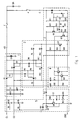
- the wiring diagram of fig. 1 shows the connections to the terminals G1 and G2 of a voltage generator of permanent magnet-type, also referred to as magnetogenerator, the connection to the positive terminal B of the battery BA, the negative terminal GND and to an auxiliary terminal C which in turn is connected to the positive terminal B of the battery BA by means of a contact K which can be actuated by means of an ignition key of a combustion engine, not shown.
- a voltage generator of permanent magnet-type also referred to as magnetogenerator
- a first power block 1 comprising a double-wave rectifier, consisting of two power diodes D2, D7 on the two branches of the bridge connected to the ground and two controlled rectifier devices, or power SCR Q1, Q4, provided in the two branches of the rectifier bridge connected between the two terminals G1 and G2 of the magnetogenerator, and the positive terminal B for the battery BA; references R1 and R7 have been used to indicate respective biasing resistances for the gates or control electrodes of Q1 and Q4.
- a bidirectional voltage suppressor D1 is branched off from the positive terminal B, while a capacitor C1, with relevant protective diode D7, is branched between the terminals G1 and G2 of the magnetogenerator.
- a reference number 2 has been used to indicate a second block for the ON-OFF switching of the power SCR Q1 and Q4;
- the circuit 2 comprises two unidirectional electronic switches consisting of low-powered SCR Q3, Q7 with their respective biasing resistances R5, R13 for polarising the gates, the current limiting resistances R3, R10, R2, R6, R8, R12, the diodes D3 and D10 for switching the power SCR Q1 and Q4, and the diodes D4, D5 whose function is to protect against reverse connections of the battery BA, and lastly the transistor Q12 for controlling the switching circuit of the low-powered SCR Q3, Q7, with the respective biasing resistances of the voltage divider R18, R22, R28, connected to a voltage measuring block.
- the voltage regulator of fig. 1 also comprises a third block 3 for measurement of the battery voltage, consisting of a programmable Zener diode Q14 as the voltage measuring element, a resistive measuring divider R11, R17, R29 with the filter capacitor C2, a protective diode D13 and a resistance R21 for the hysteresis on the battery voltage, a diode D12 for protection against a reverse connection of the battery, and the control transistors Q6, Q13 with the respective biasing resistances R15, R16 and R23, R30.
- a bidirectional voltage suppressor D6 has been inserted on the terminal C.
- the reference number 4 has been used to indicate a fourth block for synchronisation of the ON-OFF switching of the SCR Q1, Q4 with the voltage on terminals G1 and G2 of the voltage generator; the block 4 is composed of two Zener diodes D8, D9 for detecting the voltage of the magnetogenerator, the biasing resistances R20, R26, R14, R27, the transistors Q10 and Q11 for inhibiting the switching ON of the SCR Q3, Q7, whose emitter-collector circuit is connected to the voltage divider which polarises the base of Q12.
- this block 5 comprises two controlled switches connected in anti-parallel, consisting of power SCR Q2, Q5 having in series to their respective gates, two current limiting resistances R4, R9 connected to a first transistor Q8 for controlling said SCR Q2, Q5, the base of which is polarised through the resistor R24, in series with the collector-emitter circuit of a further transistor Q9 for inhibiting the first transistor Q8, in turn polarised by the resistors R19, R25 through the Zener diode D14 for detecting the presence of the battery voltage; a time delay circuit comprises a capacitor C3 which delay the operation of Q9 of the polarisation circuit; the diodes D11, D15 are for protection against a reversion of the battery, while the protective Zener diode D30 in parallel with the emitter-collector.
- the voltage regulator comprises a semicontrolled rectifier, composed of the two power diodes D2, D7 and four power SCR Q1, Q2, Q4, Q5 as shown in the diagram in fig. 1.
- the SCR Q1 and Q4 are switched by two low-powered SCR Q7 and Q3 which in turn are switched by a voltage directly from the battery BA, upon closure of the transistor Q12 when the programmable Zener diode Q14 and the transistors Q6, Q10, Q11, Q13 are inhibited.
- the capacitor C2 serves to obtain the average value of the battery voltage, while the diode D13 and the resistor R21 serve to create a hysteresis on the battery voltage in order to prevent oscillations between the inhibited and the conductive states of Q14.
- the diode D12 serves as a protection for the programmable Zener diode Q14 in the event of a reverse connection of the battery.
- the suppressors D1 and D6 which have a voltage value higher than the battery voltage value serve as a protection in the case of very high frequency voltage peaks, and before the intervention of the SCR Q2, Q5 in anti-parallel to the generator, as can occur at the disconnection of electric loads, or of the battery BA.
- the capacitor C1 serves to limit the over-voltages which may arise on the terminals G1 and G2 of the voltage generator when the SCR are switched ON or OFF.
- the Zener diodes D8, D9 with a voltage value of about 5-10 Volts higher than the battery charging voltage, bring Q10, Q11 into conduction exclusively when the phase voltage at the terminals G1 and G2 of the magnetogenerator exceeds the voltage of the Zener diodes D8, D9 thus having the possibility of switching ON the SCR Q3, Q7 which, in turn switch ON the SCR Q1, Q4 within the voltage interval only included between the battery charging voltage BA and the voltage of the aforesaid Zener diodes D8, D9, thereby avoiding the switching of the SCR Q1, Q4 with very high no-load voltages of the generator, in order to avoid over-voltages on the electric loads.
- Synchronisation is created between the no-load voltage of the magnetogenerator and the switching ON of the SCR Q1 and Q4 with considerable advantages in terms of reliability of the entire electrical voltage generating and regulating system.
- the capacitor C1 has been branched between the terminals G1 and G2 of the generator, as mentioned previously.
- a further characteristic of the voltage regulator of Fig. 1 is that, in the absence of the battery BA, the SCR Q3 and Q7 cannot be switched ON by the closure of the transistor Q12 without the source of voltage, and consequently not even the power SCR Q1 and Q4 can be activated; moreover, in the absence of the battery BA, the electric loads are isolated from the voltage generator.
- the voltage on the loads is limited by the suppressors D1 and D6.
- Said SCR Q2 and Q5 in anti-parallel to the generator, switch OFF when the current of the generator crosses zero value and remain switched OFF until the battery BA is re-connected correctly.
- the battery voltage is higher than the voltage of the Zener diode D14 which could have, for example, a voltage of 5.6 Volts; therefore the transistor Q9 conducts, while Q8 is inhibited, and the SCR Q2, Q5 in anti-parallel with respect to the terminals G1 and G2 of the generator cannot be activated by the battery voltage which is present on the emitter of Q8 from the terminal C, through the diode D11 which prevents the circulation of the current in the event of a reverse connection of the battery polarities.
- the SCR Q2, Q5 in anti-parallel to the terminals of the generator are switched ON by a command on the gate terminals by means of the resistors R4, R9, as soon as the voltage crossing the zero value, from negative to positive, polarises the base of the transistor Q8 through the resistor R24, thereby allowing the passage of the current from the emitter to the collector of Q8 until the output voltage on the terminals B and C exceeds the voltage of the Zener diode D14, putting the transistor Q9 in conduction; Q9 in turn will inhibit Q8 only after the SCR Q2 and Q5 have been switched ON.
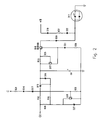
- Reference Q18 has been used to indicate a transistor for inhibiting the power supply polarised by means of the resistors R31, R39 and by the Zener diode D17 for detecting the presence of the battery voltage, and by the diode D16 for protection against a reverse connection of the battery.
- diodes D19, D20, D21 and a further Zener diode D22 for detecting the presence of the battery are the diodes D19, D20, D21 and a further Zener diode D22 for detecting the presence of the battery.
- Two transistors Q16, Q17 connected to the resistor R33 for measuring the current and to the biasing resistors R35, R38 constitute a current generator for supplying power to the LED diode D11.
- This type of indication takes place on the only two-colour LED, indicated as D11 in Fig. 2.
- This type of LED changes colour, for example red and green, in relation to the fact that the current passes through said LED in either direction.
- the voltage present on terminal C definitely exceeds the voltage of the Zener diode D17 typically 5.6 Volts, and bias or polarises the base of the transistor Q18 whose collector is closed to ground, preventing the switching ON of the SCR Q15 which together with the large-capacity capacitor C4, for example 1000 microfarads, constitutes the power supply of the indicator system.
- the transistor Q18 is inhibited and the SCR Q15 is switched ON by means of the resistors R34 R36, connecting one of the two terminals G1 and G2 of the generator to the capacitor C4 and charging it up to the voltage of the Zener diode D23, for example 5.6 Volts.
- the diodes D20 and D21 serve to prevent the circulation of current when the battery is reversely connected.
- the transistors Q16 and Q17 together with the resistors R33, R35 and R38 constitute a generator of a current whose value is given by the base-emitter threshold voltage of Q17, divided by the value of R33.
Landscapes
- Engineering & Computer Science (AREA)
- Power Engineering (AREA)
- Control Of Eletrric Generators (AREA)
- Control Of Charge By Means Of Generators (AREA)
Applications Claiming Priority (1)
| Application Number | Priority Date | Filing Date | Title |
|---|---|---|---|
| IT001979A ITMI20041979A1 (it) | 2004-10-19 | 2004-10-19 | Regolatore di tensione per generatori a magneti permanenti per applicazioni nei motori stazionari, protetto da errate connessioni |
Publications (3)
| Publication Number | Publication Date |
|---|---|
| EP1650848A2 true EP1650848A2 (de) | 2006-04-26 |
| EP1650848A3 EP1650848A3 (de) | 2010-07-14 |
| EP1650848B1 EP1650848B1 (de) | 2011-09-28 |
Family
ID=35759272
Family Applications (1)
| Application Number | Title | Priority Date | Filing Date |
|---|---|---|---|
| EP05022556A Expired - Lifetime EP1650848B1 (de) | 2004-10-19 | 2005-10-17 | Spannungsregler für vor falschen Anschlüssen geschütze Magnetogeneratoren |
Country Status (3)
| Country | Link |
|---|---|
| EP (1) | EP1650848B1 (de) |
| AT (1) | ATE526716T1 (de) |
| IT (1) | ITMI20041979A1 (de) |
Family Cites Families (4)
| Publication number | Priority date | Publication date | Assignee | Title |
|---|---|---|---|---|
| US3930197A (en) * | 1974-04-25 | 1975-12-30 | Frederick A Saylor | Voltage regulator system |
| US4701692A (en) * | 1985-02-15 | 1987-10-20 | Nippondenso Co., Ltd. | Rectifying system for magnet-type AC generator |
| US6181111B1 (en) * | 1999-07-21 | 2001-01-30 | Lowell T. Hoffman | Permanent magnet alternator system for battery charging |
| WO2002049184A1 (en) * | 2000-12-13 | 2002-06-20 | Satcon Technology Corporation | Motor vehicle alternator having a single voltage sensor and a half-wave controlled rectifier bridge for increasing output |
-
2004
- 2004-10-19 IT IT001979A patent/ITMI20041979A1/it unknown
-
2005
- 2005-10-17 AT AT05022556T patent/ATE526716T1/de not_active IP Right Cessation
- 2005-10-17 EP EP05022556A patent/EP1650848B1/de not_active Expired - Lifetime
Also Published As
| Publication number | Publication date |
|---|---|
| ITMI20041979A1 (it) | 2005-01-19 |
| ATE526716T1 (de) | 2011-10-15 |
| EP1650848A3 (de) | 2010-07-14 |
| EP1650848B1 (de) | 2011-09-28 |
Similar Documents
| Publication | Publication Date | Title |
|---|---|---|
| US6154081A (en) | Load circuit having extended reverse voltage protection | |
| US10566785B2 (en) | Surge protective device with abnormal overvoltage protection | |
| CN110100363B (zh) | 电路保护装置以及电压检测装置 | |
| CN107431348B (zh) | 被保护免受过压的电子控制设备 | |
| HU222801B1 (hu) | Kapcsolási elrendezés háromfázisú generátor kimeneti feszültségének szabályozására | |
| GB2368206A (en) | Protection of intrinsically safe circuits | |
| CN102545145B (zh) | 用于保护功耗电路的系统和方法 | |
| US8649145B2 (en) | Circuit arrangement for limiting a voltage | |
| KR100421094B1 (ko) | 차량용 발전기의 외장형 레귤레이터 | |
| EP1650848B1 (de) | Spannungsregler für vor falschen Anschlüssen geschütze Magnetogeneratoren | |
| CN210577795U (zh) | 一种带超温保护功能的双通道直流浪涌抑制电路 | |
| US3943408A (en) | Over-voltage protection circuit for wye connected electric machine | |
| US3406318A (en) | Potential regulator with an electrical polarity reversal protection feature | |
| GB2056808A (en) | Power transistor protection | |
| JPH1032940A (ja) | 車両用交流発電機の制御装置 | |
| US4167170A (en) | Turn-off protected ignition system for internal combustion engines | |
| EP2701256B1 (de) | Vorrichtungen und Verfahren zum Überspannungsschutz | |
| US7369383B2 (en) | Protective circuit | |
| CN210927073U (zh) | 一种过压保护装置及一种车辆 | |
| CN213637510U (zh) | 一种具有高响应的开关控制的电量补偿保护电路 | |
| CN215990270U (zh) | 一种用于保护卫星终端铅酸电池的控制电路 | |
| RU2254656C1 (ru) | Устройство для защиты трехфазного электродвигателя от аварийных режимов работы | |
| CN211790740U (zh) | 一种保护电路 | |
| CN214069559U (zh) | 一种具有多种保护功能的直流电源滤波器电路 | |
| JPH0232858B2 (de) |
Legal Events
| Date | Code | Title | Description |
|---|---|---|---|
| PUAI | Public reference made under article 153(3) epc to a published international application that has entered the european phase |
Free format text: ORIGINAL CODE: 0009012 |
|
| AK | Designated contracting states |
Kind code of ref document: A2 Designated state(s): AT BE BG CH CY CZ DE DK EE ES FI FR GB GR HU IE IS IT LI LT LU LV MC NL PL PT RO SE SI SK TR |
|
| AX | Request for extension of the european patent |
Extension state: AL BA HR MK YU |
|
| PUAL | Search report despatched |
Free format text: ORIGINAL CODE: 0009013 |
|
| AK | Designated contracting states |
Kind code of ref document: A3 Designated state(s): AT BE BG CH CY CZ DE DK EE ES FI FR GB GR HU IE IS IT LI LT LU LV MC NL PL PT RO SE SI SK TR |
|
| AX | Request for extension of the european patent |
Extension state: AL BA HR MK YU |
|
| 17P | Request for examination filed |
Effective date: 20110113 |
|
| AKX | Designation fees paid |
Designated state(s): AT BE BG CH CY CZ DE DK EE ES FI FR GB GR HU IE IS IT LI LT LU LV MC NL PL PT RO SE SI SK TR |
|
| GRAP | Despatch of communication of intention to grant a patent |
Free format text: ORIGINAL CODE: EPIDOSNIGR1 |
|
| RIC1 | Information provided on ipc code assigned before grant |
Ipc: H02J 7/14 20060101AFI20110311BHEP |
|
| GRAS | Grant fee paid |
Free format text: ORIGINAL CODE: EPIDOSNIGR3 |
|
| GRAA | (expected) grant |
Free format text: ORIGINAL CODE: 0009210 |
|
| AK | Designated contracting states |
Kind code of ref document: B1 Designated state(s): AT BE BG CH CY CZ DE DK EE ES FI FR GB GR HU IE IS IT LI LT LU LV MC NL PL PT RO SE SI SK TR |
|
| REG | Reference to a national code |
Ref country code: GB Ref legal event code: FG4D |
|
| REG | Reference to a national code |
Ref country code: CH Ref legal event code: EP |
|
| REG | Reference to a national code |
Ref country code: IE Ref legal event code: FG4D |
|
| REG | Reference to a national code |
Ref country code: DE Ref legal event code: R096 Ref document number: 602005030197 Country of ref document: DE Effective date: 20111124 |
|
| REG | Reference to a national code |
Ref country code: NL Ref legal event code: VDEP Effective date: 20110928 |
|
| PG25 | Lapsed in a contracting state [announced via postgrant information from national office to epo] |
Ref country code: LT Free format text: LAPSE BECAUSE OF FAILURE TO SUBMIT A TRANSLATION OF THE DESCRIPTION OR TO PAY THE FEE WITHIN THE PRESCRIBED TIME-LIMIT Effective date: 20110928 Ref country code: SE Free format text: LAPSE BECAUSE OF FAILURE TO SUBMIT A TRANSLATION OF THE DESCRIPTION OR TO PAY THE FEE WITHIN THE PRESCRIBED TIME-LIMIT Effective date: 20110928 Ref country code: FI Free format text: LAPSE BECAUSE OF FAILURE TO SUBMIT A TRANSLATION OF THE DESCRIPTION OR TO PAY THE FEE WITHIN THE PRESCRIBED TIME-LIMIT Effective date: 20110928 |
|
| LTIE | Lt: invalidation of european patent or patent extension |
Effective date: 20110928 |
|
| PG25 | Lapsed in a contracting state [announced via postgrant information from national office to epo] |
Ref country code: LV Free format text: LAPSE BECAUSE OF FAILURE TO SUBMIT A TRANSLATION OF THE DESCRIPTION OR TO PAY THE FEE WITHIN THE PRESCRIBED TIME-LIMIT Effective date: 20110928 Ref country code: CY Free format text: LAPSE BECAUSE OF FAILURE TO SUBMIT A TRANSLATION OF THE DESCRIPTION OR TO PAY THE FEE WITHIN THE PRESCRIBED TIME-LIMIT Effective date: 20110928 Ref country code: AT Free format text: LAPSE BECAUSE OF FAILURE TO SUBMIT A TRANSLATION OF THE DESCRIPTION OR TO PAY THE FEE WITHIN THE PRESCRIBED TIME-LIMIT Effective date: 20110928 Ref country code: SI Free format text: LAPSE BECAUSE OF FAILURE TO SUBMIT A TRANSLATION OF THE DESCRIPTION OR TO PAY THE FEE WITHIN THE PRESCRIBED TIME-LIMIT Effective date: 20110928 Ref country code: GR Free format text: LAPSE BECAUSE OF FAILURE TO SUBMIT A TRANSLATION OF THE DESCRIPTION OR TO PAY THE FEE WITHIN THE PRESCRIBED TIME-LIMIT Effective date: 20111229 |
|
| REG | Reference to a national code |
Ref country code: AT Ref legal event code: MK05 Ref document number: 526716 Country of ref document: AT Kind code of ref document: T Effective date: 20110928 |
|
| PG25 | Lapsed in a contracting state [announced via postgrant information from national office to epo] |
Ref country code: BE Free format text: LAPSE BECAUSE OF FAILURE TO SUBMIT A TRANSLATION OF THE DESCRIPTION OR TO PAY THE FEE WITHIN THE PRESCRIBED TIME-LIMIT Effective date: 20110928 |
|
| PG25 | Lapsed in a contracting state [announced via postgrant information from national office to epo] |
Ref country code: CZ Free format text: LAPSE BECAUSE OF FAILURE TO SUBMIT A TRANSLATION OF THE DESCRIPTION OR TO PAY THE FEE WITHIN THE PRESCRIBED TIME-LIMIT Effective date: 20110928 Ref country code: SK Free format text: LAPSE BECAUSE OF FAILURE TO SUBMIT A TRANSLATION OF THE DESCRIPTION OR TO PAY THE FEE WITHIN THE PRESCRIBED TIME-LIMIT Effective date: 20110928 Ref country code: IS Free format text: LAPSE BECAUSE OF FAILURE TO SUBMIT A TRANSLATION OF THE DESCRIPTION OR TO PAY THE FEE WITHIN THE PRESCRIBED TIME-LIMIT Effective date: 20120128 |
|
| PG25 | Lapsed in a contracting state [announced via postgrant information from national office to epo] |
Ref country code: MC Free format text: LAPSE BECAUSE OF NON-PAYMENT OF DUE FEES Effective date: 20111031 Ref country code: EE Free format text: LAPSE BECAUSE OF FAILURE TO SUBMIT A TRANSLATION OF THE DESCRIPTION OR TO PAY THE FEE WITHIN THE PRESCRIBED TIME-LIMIT Effective date: 20110928 Ref country code: NL Free format text: LAPSE BECAUSE OF FAILURE TO SUBMIT A TRANSLATION OF THE DESCRIPTION OR TO PAY THE FEE WITHIN THE PRESCRIBED TIME-LIMIT Effective date: 20110928 Ref country code: RO Free format text: LAPSE BECAUSE OF FAILURE TO SUBMIT A TRANSLATION OF THE DESCRIPTION OR TO PAY THE FEE WITHIN THE PRESCRIBED TIME-LIMIT Effective date: 20110928 Ref country code: PT Free format text: LAPSE BECAUSE OF FAILURE TO SUBMIT A TRANSLATION OF THE DESCRIPTION OR TO PAY THE FEE WITHIN THE PRESCRIBED TIME-LIMIT Effective date: 20120130 |
|
| REG | Reference to a national code |
Ref country code: CH Ref legal event code: PL |
|
| PG25 | Lapsed in a contracting state [announced via postgrant information from national office to epo] |
Ref country code: DK Free format text: LAPSE BECAUSE OF FAILURE TO SUBMIT A TRANSLATION OF THE DESCRIPTION OR TO PAY THE FEE WITHIN THE PRESCRIBED TIME-LIMIT Effective date: 20110928 Ref country code: LI Free format text: LAPSE BECAUSE OF NON-PAYMENT OF DUE FEES Effective date: 20111031 Ref country code: CH Free format text: LAPSE BECAUSE OF NON-PAYMENT OF DUE FEES Effective date: 20111031 |
|
| REG | Reference to a national code |
Ref country code: IE Ref legal event code: MM4A |
|
| PLBE | No opposition filed within time limit |
Free format text: ORIGINAL CODE: 0009261 |
|
| STAA | Information on the status of an ep patent application or granted ep patent |
Free format text: STATUS: NO OPPOSITION FILED WITHIN TIME LIMIT |
|
| PG25 | Lapsed in a contracting state [announced via postgrant information from national office to epo] |
Ref country code: PL Free format text: LAPSE BECAUSE OF FAILURE TO SUBMIT A TRANSLATION OF THE DESCRIPTION OR TO PAY THE FEE WITHIN THE PRESCRIBED TIME-LIMIT Effective date: 20110928 |
|
| 26N | No opposition filed |
Effective date: 20120629 |
|
| REG | Reference to a national code |
Ref country code: DE Ref legal event code: R097 Ref document number: 602005030197 Country of ref document: DE Effective date: 20120629 |
|
| PG25 | Lapsed in a contracting state [announced via postgrant information from national office to epo] |
Ref country code: IE Free format text: LAPSE BECAUSE OF NON-PAYMENT OF DUE FEES Effective date: 20111017 |
|
| PG25 | Lapsed in a contracting state [announced via postgrant information from national office to epo] |
Ref country code: ES Free format text: LAPSE BECAUSE OF FAILURE TO SUBMIT A TRANSLATION OF THE DESCRIPTION OR TO PAY THE FEE WITHIN THE PRESCRIBED TIME-LIMIT Effective date: 20120108 |
|
| PG25 | Lapsed in a contracting state [announced via postgrant information from national office to epo] |
Ref country code: LU Free format text: LAPSE BECAUSE OF NON-PAYMENT OF DUE FEES Effective date: 20111017 |
|
| PG25 | Lapsed in a contracting state [announced via postgrant information from national office to epo] |
Ref country code: BG Free format text: LAPSE BECAUSE OF FAILURE TO SUBMIT A TRANSLATION OF THE DESCRIPTION OR TO PAY THE FEE WITHIN THE PRESCRIBED TIME-LIMIT Effective date: 20111228 |
|
| PG25 | Lapsed in a contracting state [announced via postgrant information from national office to epo] |
Ref country code: TR Free format text: LAPSE BECAUSE OF FAILURE TO SUBMIT A TRANSLATION OF THE DESCRIPTION OR TO PAY THE FEE WITHIN THE PRESCRIBED TIME-LIMIT Effective date: 20110928 |
|
| PG25 | Lapsed in a contracting state [announced via postgrant information from national office to epo] |
Ref country code: HU Free format text: LAPSE BECAUSE OF FAILURE TO SUBMIT A TRANSLATION OF THE DESCRIPTION OR TO PAY THE FEE WITHIN THE PRESCRIBED TIME-LIMIT Effective date: 20110928 |
|
| REG | Reference to a national code |
Ref country code: FR Ref legal event code: PLFP Year of fee payment: 11 |
|
| REG | Reference to a national code |
Ref country code: FR Ref legal event code: PLFP Year of fee payment: 12 |
|
| REG | Reference to a national code |
Ref country code: FR Ref legal event code: PLFP Year of fee payment: 13 |
|
| REG | Reference to a national code |
Ref country code: FR Ref legal event code: PLFP Year of fee payment: 14 |
|
| P01 | Opt-out of the competence of the unified patent court (upc) registered |
Effective date: 20230527 |
|
| PGFP | Annual fee paid to national office [announced via postgrant information from national office to epo] |
Ref country code: DE Payment date: 20241029 Year of fee payment: 20 |
|
| PGFP | Annual fee paid to national office [announced via postgrant information from national office to epo] |
Ref country code: GB Payment date: 20241028 Year of fee payment: 20 |
|
| PGFP | Annual fee paid to national office [announced via postgrant information from national office to epo] |
Ref country code: FR Payment date: 20241025 Year of fee payment: 20 |
|
| PGFP | Annual fee paid to national office [announced via postgrant information from national office to epo] |
Ref country code: IT Payment date: 20241018 Year of fee payment: 20 |
|
| REG | Reference to a national code |
Ref country code: DE Ref legal event code: R071 Ref document number: 602005030197 Country of ref document: DE |
|
| REG | Reference to a national code |
Ref country code: GB Ref legal event code: PE20 Expiry date: 20251016 |