EP1650734A1 - Display device and driving method thereof - Google Patents
Display device and driving method thereof Download PDFInfo
- Publication number
- EP1650734A1 EP1650734A1 EP05106560A EP05106560A EP1650734A1 EP 1650734 A1 EP1650734 A1 EP 1650734A1 EP 05106560 A EP05106560 A EP 05106560A EP 05106560 A EP05106560 A EP 05106560A EP 1650734 A1 EP1650734 A1 EP 1650734A1
- Authority
- EP
- European Patent Office
- Prior art keywords
- subfields
- group
- light
- row
- subfield
- Prior art date
- Legal status (The legal status is an assumption and is not a legal conclusion. Google has not performed a legal analysis and makes no representation as to the accuracy of the status listed.)
- Withdrawn
Links
Images



Classifications
-
- G—PHYSICS
- G09—EDUCATION; CRYPTOGRAPHY; DISPLAY; ADVERTISING; SEALS
- G09G—ARRANGEMENTS OR CIRCUITS FOR CONTROL OF INDICATING DEVICES USING STATIC MEANS TO PRESENT VARIABLE INFORMATION
- G09G3/00—Control arrangements or circuits, of interest only in connection with visual indicators other than cathode-ray tubes
- G09G3/20—Control arrangements or circuits, of interest only in connection with visual indicators other than cathode-ray tubes for presentation of an assembly of a number of characters, e.g. a page, by composing the assembly by combination of individual elements arranged in a matrix no fixed position being assigned to or needed to be assigned to the individual characters or partial characters
- G09G3/22—Control arrangements or circuits, of interest only in connection with visual indicators other than cathode-ray tubes for presentation of an assembly of a number of characters, e.g. a page, by composing the assembly by combination of individual elements arranged in a matrix no fixed position being assigned to or needed to be assigned to the individual characters or partial characters using controlled light sources
- G09G3/28—Control arrangements or circuits, of interest only in connection with visual indicators other than cathode-ray tubes for presentation of an assembly of a number of characters, e.g. a page, by composing the assembly by combination of individual elements arranged in a matrix no fixed position being assigned to or needed to be assigned to the individual characters or partial characters using controlled light sources using luminous gas-discharge panels, e.g. plasma panels
- G09G3/288—Control arrangements or circuits, of interest only in connection with visual indicators other than cathode-ray tubes for presentation of an assembly of a number of characters, e.g. a page, by composing the assembly by combination of individual elements arranged in a matrix no fixed position being assigned to or needed to be assigned to the individual characters or partial characters using controlled light sources using luminous gas-discharge panels, e.g. plasma panels using AC panels
- G09G3/291—Control arrangements or circuits, of interest only in connection with visual indicators other than cathode-ray tubes for presentation of an assembly of a number of characters, e.g. a page, by composing the assembly by combination of individual elements arranged in a matrix no fixed position being assigned to or needed to be assigned to the individual characters or partial characters using controlled light sources using luminous gas-discharge panels, e.g. plasma panels using AC panels controlling the gas discharge to control a cell condition, e.g. by means of specific pulse shapes
- G09G3/294—Control arrangements or circuits, of interest only in connection with visual indicators other than cathode-ray tubes for presentation of an assembly of a number of characters, e.g. a page, by composing the assembly by combination of individual elements arranged in a matrix no fixed position being assigned to or needed to be assigned to the individual characters or partial characters using controlled light sources using luminous gas-discharge panels, e.g. plasma panels using AC panels controlling the gas discharge to control a cell condition, e.g. by means of specific pulse shapes for lighting or sustain discharge
-
- G—PHYSICS
- G09—EDUCATION; CRYPTOGRAPHY; DISPLAY; ADVERTISING; SEALS
- G09G—ARRANGEMENTS OR CIRCUITS FOR CONTROL OF INDICATING DEVICES USING STATIC MEANS TO PRESENT VARIABLE INFORMATION
- G09G3/00—Control arrangements or circuits, of interest only in connection with visual indicators other than cathode-ray tubes
- G09G3/20—Control arrangements or circuits, of interest only in connection with visual indicators other than cathode-ray tubes for presentation of an assembly of a number of characters, e.g. a page, by composing the assembly by combination of individual elements arranged in a matrix no fixed position being assigned to or needed to be assigned to the individual characters or partial characters
- G09G3/22—Control arrangements or circuits, of interest only in connection with visual indicators other than cathode-ray tubes for presentation of an assembly of a number of characters, e.g. a page, by composing the assembly by combination of individual elements arranged in a matrix no fixed position being assigned to or needed to be assigned to the individual characters or partial characters using controlled light sources
- G09G3/28—Control arrangements or circuits, of interest only in connection with visual indicators other than cathode-ray tubes for presentation of an assembly of a number of characters, e.g. a page, by composing the assembly by combination of individual elements arranged in a matrix no fixed position being assigned to or needed to be assigned to the individual characters or partial characters using controlled light sources using luminous gas-discharge panels, e.g. plasma panels
- G09G3/288—Control arrangements or circuits, of interest only in connection with visual indicators other than cathode-ray tubes for presentation of an assembly of a number of characters, e.g. a page, by composing the assembly by combination of individual elements arranged in a matrix no fixed position being assigned to or needed to be assigned to the individual characters or partial characters using controlled light sources using luminous gas-discharge panels, e.g. plasma panels using AC panels
- G09G3/291—Control arrangements or circuits, of interest only in connection with visual indicators other than cathode-ray tubes for presentation of an assembly of a number of characters, e.g. a page, by composing the assembly by combination of individual elements arranged in a matrix no fixed position being assigned to or needed to be assigned to the individual characters or partial characters using controlled light sources using luminous gas-discharge panels, e.g. plasma panels using AC panels controlling the gas discharge to control a cell condition, e.g. by means of specific pulse shapes
- G09G3/293—Control arrangements or circuits, of interest only in connection with visual indicators other than cathode-ray tubes for presentation of an assembly of a number of characters, e.g. a page, by composing the assembly by combination of individual elements arranged in a matrix no fixed position being assigned to or needed to be assigned to the individual characters or partial characters using controlled light sources using luminous gas-discharge panels, e.g. plasma panels using AC panels controlling the gas discharge to control a cell condition, e.g. by means of specific pulse shapes for address discharge
- G09G3/2937—Control arrangements or circuits, of interest only in connection with visual indicators other than cathode-ray tubes for presentation of an assembly of a number of characters, e.g. a page, by composing the assembly by combination of individual elements arranged in a matrix no fixed position being assigned to or needed to be assigned to the individual characters or partial characters using controlled light sources using luminous gas-discharge panels, e.g. plasma panels using AC panels controlling the gas discharge to control a cell condition, e.g. by means of specific pulse shapes for address discharge being addressed only once per frame
-
- G—PHYSICS
- G09—EDUCATION; CRYPTOGRAPHY; DISPLAY; ADVERTISING; SEALS
- G09G—ARRANGEMENTS OR CIRCUITS FOR CONTROL OF INDICATING DEVICES USING STATIC MEANS TO PRESENT VARIABLE INFORMATION
- G09G3/00—Control arrangements or circuits, of interest only in connection with visual indicators other than cathode-ray tubes
- G09G3/20—Control arrangements or circuits, of interest only in connection with visual indicators other than cathode-ray tubes for presentation of an assembly of a number of characters, e.g. a page, by composing the assembly by combination of individual elements arranged in a matrix no fixed position being assigned to or needed to be assigned to the individual characters or partial characters
- G09G3/22—Control arrangements or circuits, of interest only in connection with visual indicators other than cathode-ray tubes for presentation of an assembly of a number of characters, e.g. a page, by composing the assembly by combination of individual elements arranged in a matrix no fixed position being assigned to or needed to be assigned to the individual characters or partial characters using controlled light sources
- G09G3/28—Control arrangements or circuits, of interest only in connection with visual indicators other than cathode-ray tubes for presentation of an assembly of a number of characters, e.g. a page, by composing the assembly by combination of individual elements arranged in a matrix no fixed position being assigned to or needed to be assigned to the individual characters or partial characters using controlled light sources using luminous gas-discharge panels, e.g. plasma panels
- G09G3/288—Control arrangements or circuits, of interest only in connection with visual indicators other than cathode-ray tubes for presentation of an assembly of a number of characters, e.g. a page, by composing the assembly by combination of individual elements arranged in a matrix no fixed position being assigned to or needed to be assigned to the individual characters or partial characters using controlled light sources using luminous gas-discharge panels, e.g. plasma panels using AC panels
- G09G3/291—Control arrangements or circuits, of interest only in connection with visual indicators other than cathode-ray tubes for presentation of an assembly of a number of characters, e.g. a page, by composing the assembly by combination of individual elements arranged in a matrix no fixed position being assigned to or needed to be assigned to the individual characters or partial characters using controlled light sources using luminous gas-discharge panels, e.g. plasma panels using AC panels controlling the gas discharge to control a cell condition, e.g. by means of specific pulse shapes
- G09G3/293—Control arrangements or circuits, of interest only in connection with visual indicators other than cathode-ray tubes for presentation of an assembly of a number of characters, e.g. a page, by composing the assembly by combination of individual elements arranged in a matrix no fixed position being assigned to or needed to be assigned to the individual characters or partial characters using controlled light sources using luminous gas-discharge panels, e.g. plasma panels using AC panels controlling the gas discharge to control a cell condition, e.g. by means of specific pulse shapes for address discharge
- G09G3/2932—Addressed by writing selected cells that are in an OFF state
-
- G—PHYSICS
- G09—EDUCATION; CRYPTOGRAPHY; DISPLAY; ADVERTISING; SEALS
- G09G—ARRANGEMENTS OR CIRCUITS FOR CONTROL OF INDICATING DEVICES USING STATIC MEANS TO PRESENT VARIABLE INFORMATION
- G09G3/00—Control arrangements or circuits, of interest only in connection with visual indicators other than cathode-ray tubes
- G09G3/20—Control arrangements or circuits, of interest only in connection with visual indicators other than cathode-ray tubes for presentation of an assembly of a number of characters, e.g. a page, by composing the assembly by combination of individual elements arranged in a matrix no fixed position being assigned to or needed to be assigned to the individual characters or partial characters
- G09G3/22—Control arrangements or circuits, of interest only in connection with visual indicators other than cathode-ray tubes for presentation of an assembly of a number of characters, e.g. a page, by composing the assembly by combination of individual elements arranged in a matrix no fixed position being assigned to or needed to be assigned to the individual characters or partial characters using controlled light sources
- G09G3/28—Control arrangements or circuits, of interest only in connection with visual indicators other than cathode-ray tubes for presentation of an assembly of a number of characters, e.g. a page, by composing the assembly by combination of individual elements arranged in a matrix no fixed position being assigned to or needed to be assigned to the individual characters or partial characters using controlled light sources using luminous gas-discharge panels, e.g. plasma panels
- G09G3/288—Control arrangements or circuits, of interest only in connection with visual indicators other than cathode-ray tubes for presentation of an assembly of a number of characters, e.g. a page, by composing the assembly by combination of individual elements arranged in a matrix no fixed position being assigned to or needed to be assigned to the individual characters or partial characters using controlled light sources using luminous gas-discharge panels, e.g. plasma panels using AC panels
- G09G3/291—Control arrangements or circuits, of interest only in connection with visual indicators other than cathode-ray tubes for presentation of an assembly of a number of characters, e.g. a page, by composing the assembly by combination of individual elements arranged in a matrix no fixed position being assigned to or needed to be assigned to the individual characters or partial characters using controlled light sources using luminous gas-discharge panels, e.g. plasma panels using AC panels controlling the gas discharge to control a cell condition, e.g. by means of specific pulse shapes
- G09G3/293—Control arrangements or circuits, of interest only in connection with visual indicators other than cathode-ray tubes for presentation of an assembly of a number of characters, e.g. a page, by composing the assembly by combination of individual elements arranged in a matrix no fixed position being assigned to or needed to be assigned to the individual characters or partial characters using controlled light sources using luminous gas-discharge panels, e.g. plasma panels using AC panels controlling the gas discharge to control a cell condition, e.g. by means of specific pulse shapes for address discharge
- G09G3/2935—Addressed by erasing selected cells that are in an ON state
-
- G—PHYSICS
- G09—EDUCATION; CRYPTOGRAPHY; DISPLAY; ADVERTISING; SEALS
- G09G—ARRANGEMENTS OR CIRCUITS FOR CONTROL OF INDICATING DEVICES USING STATIC MEANS TO PRESENT VARIABLE INFORMATION
- G09G3/00—Control arrangements or circuits, of interest only in connection with visual indicators other than cathode-ray tubes
- G09G3/20—Control arrangements or circuits, of interest only in connection with visual indicators other than cathode-ray tubes for presentation of an assembly of a number of characters, e.g. a page, by composing the assembly by combination of individual elements arranged in a matrix no fixed position being assigned to or needed to be assigned to the individual characters or partial characters
- G09G3/22—Control arrangements or circuits, of interest only in connection with visual indicators other than cathode-ray tubes for presentation of an assembly of a number of characters, e.g. a page, by composing the assembly by combination of individual elements arranged in a matrix no fixed position being assigned to or needed to be assigned to the individual characters or partial characters using controlled light sources
- G09G3/28—Control arrangements or circuits, of interest only in connection with visual indicators other than cathode-ray tubes for presentation of an assembly of a number of characters, e.g. a page, by composing the assembly by combination of individual elements arranged in a matrix no fixed position being assigned to or needed to be assigned to the individual characters or partial characters using controlled light sources using luminous gas-discharge panels, e.g. plasma panels
- G09G3/288—Control arrangements or circuits, of interest only in connection with visual indicators other than cathode-ray tubes for presentation of an assembly of a number of characters, e.g. a page, by composing the assembly by combination of individual elements arranged in a matrix no fixed position being assigned to or needed to be assigned to the individual characters or partial characters using controlled light sources using luminous gas-discharge panels, e.g. plasma panels using AC panels
- G09G3/296—Driving circuits for producing the waveforms applied to the driving electrodes
-
- G—PHYSICS
- G09—EDUCATION; CRYPTOGRAPHY; DISPLAY; ADVERTISING; SEALS
- G09G—ARRANGEMENTS OR CIRCUITS FOR CONTROL OF INDICATING DEVICES USING STATIC MEANS TO PRESENT VARIABLE INFORMATION
- G09G2310/00—Command of the display device
- G09G2310/02—Addressing, scanning or driving the display screen or processing steps related thereto
- G09G2310/0202—Addressing of scan or signal lines
- G09G2310/0216—Interleaved control phases for different scan lines in the same sub-field, e.g. initialization, addressing and sustaining in plasma displays that are not simultaneous for all scan lines
-
- G—PHYSICS
- G09—EDUCATION; CRYPTOGRAPHY; DISPLAY; ADVERTISING; SEALS
- G09G—ARRANGEMENTS OR CIRCUITS FOR CONTROL OF INDICATING DEVICES USING STATIC MEANS TO PRESENT VARIABLE INFORMATION
- G09G2310/00—Command of the display device
- G09G2310/02—Addressing, scanning or driving the display screen or processing steps related thereto
- G09G2310/0202—Addressing of scan or signal lines
- G09G2310/0218—Addressing of scan or signal lines with collection of electrodes in groups for n-dimensional addressing
Definitions
- the present invention relates to a display device and a driving method thereof, and more particularly, to a driving method for representing gray scales using subfields.
- one field (1TV field) is divided into a plurality of subfields, and each subfield has an assigned weight.
- Gray scales are represented by combining weights of active (i.e., displayed) subfields of the plurality of subfields.
- Each subfield typically includes an address period, during which discharge cells to be lit are selected, and a sustain period, during which the selected discharge cells are sustain discharged during a period corresponding to the subfield's weight.
- An address display separation (ADS) driving method includes performing a sustain discharge operation for all discharge cells after addressing all discharge cells in each subfield.
- the address period is separate from the sustain period.
- the ADS method can be easily implemented, but since the addressing operation is sequentially performed for all discharge cells, some discharge cells to be addressed in the latter stages of the address period may not actually get addressed due to lack of priming particles within the discharge cells. Therefore, to secure a stable addressing operation, the width of scan pulses sequentially applied to row electrodes may be increased, but this lengthens the address period. Consequently, the subfields also become longer, which limits the number of subfields available in one field.
- an address while display (AWD) driving method includes inserting an address pulse for each line between two successive sustain discharge pulses and performing the addressing operation for one line while performing the sustain discharge operation for another line.
- the address period is not separate from the sustain period.
- a relatively lengthy reset pulse is inserted between an address pulse and a sustain discharge pulse.
- a strong reset discharge may cause a black screen to be seen brightly, thereby deteriorating contrast ratio.
- both the ADS method and the AWD method may use different weighted subfields to represent gray scales. For example, with subfields having weights of a type of the second power of 2, a so-called false contour may be produced when one discharge cell represents a 127 th gray scale level in one frame and a 128 th gray scale level in a following frame.
- the present invention provides a driving method of a display device, which is capable of performing a high speed scan operation.
- the present invention also provides a driving method of a display device, which is capable of reducing false contour.
- the present invention also provides a driving method of a display device, which is capable of improving contrast ratio.
- the present invention also provides a driving method of grouping a plurality of subfields into groups of subfields for setting light-emitting cells through write discharge and groups of subfields for setting non-light-emitting cells through erase discharge after setting the light-emitting cells through the write discharge.
- the present invention discloses a driving method of dividing one field into a plurality of subfields and representing a gray scale using the plurality of subfields in a display device including a plurality of row electrodes, a plurality of column electrodes intersecting the plurality of row electrodes, and a plurality of discharge cells defined by the plurality of row electrodes and the plurality of column electrodes.
- the plurality of row electrodes is grouped into a plurality of row groups, each subfield is divided into a plurality of select periods respectively corresponding to the plurality of row groups, and the plurality of subfields is grouped into a plurality of subfield groups.
- a select period for a first row group of a first group of subfields light-emitting cells are selected from discharge cells of the first row group, and the light-emitting cells of the first row group are set to non-light-emitting cells after the light-emitting cells are sustain-discharged during a sustain period.
- a select period for the first row group of a first subfield which is positioned at the head in time, of a second group of subfields
- light-emitting cells are selected from discharge cells of the first row group and the light-emitting cells are sustain-discharged during a sustain period.
- non-light-emitting cells are selected from the light-emitting cells of the first row group and remaining light-emitting cells are sustain-discharged during a sustain period.
- the present invention also discloses a driving method of dividing one field into a plurality of subfields and representing a gray scale using the plurality of subfields in a display device including a plurality of row electrodes, a plurality of column electrodes intersecting the plurality of row electrodes, and a plurality of discharge cells defined by the plurality of row electrodes and the plurality of column electrodes.
- the plurality of subfields is grouped into a first group of subfields including a minimal weight subfield, a second group of subfields, and a third group of subfields including at least two consecutive subfields.
- the plurality of row electrodes is grouped into a plurality of row groups in the third group of subfields, and the plurality of row electrodes is grouped into a number of row groups corresponding to a weight of a subfield for each subfield in the second group of subfields.
- each subfield is divided into a plurality of select periods respectively corresponding to the plurality of row groups.
- light-emitting cells are selected in the plurality of row electrodes, and the light-emitting cells are discharged during a period corresponding to a weight of a corresponding subfield.
- a select period for a first row group of the second group of subfields light-emitting cells are selected from discharge cells of the first row group, and the light-emitting cells are discharged during a sustain period.
- a select period for a second row group of a first subfield which is positioned at the head in time, of the third group of subfields
- light-emitting cells are selected from discharge cells of the second row group, and the light-emitting cells are discharged during a sustain period.
- non-light-emitting cells are selected from the light-emitting cells of the second row group, and remaining light-emitting cells are discharged during a sustain period.
- the method further comprises: in a select period for a third row group of the second group of subfields, light-emitting cells from discharge cells of the third row group are selected and the light-emitting cells of the third row group during a sustain period are discharged; in a select period for a fourth row group of the first subfield, light-emitting cells from discharge cells of the fourth row group are selected and the light-emitting cells of the fourth row group during a sustain period are discharged; and in a select period for the fourth row group of the second subfield, non-light-emitting cells from the light-emitting cells of the fourth row group are selected and remaining light-emitting cells of the fourth row group during a sustain period are discharged.
- light-emitting cells of the second row group are discharged during a sustain period of a select period for the fourth row group.
- a length of a sustain period of a select period for the second row group is equal to a length of the sustain period of the select period for the fourth row group.
- the light-emitting cells of the first row group are set to non-light-emitting cells after a specific period elapses.
- the specific period is a period during which sustain discharge for a period corresponding to a weight of a corresponding subfield of the first row group is completed.
- a sustain period is performed for the light-emitting cells of the third row group.
- sustain discharge is performed after selecting light-emitting cells for all row electrodes.
- the plurality of row electrodes is grouped into at least two row groups, and the wherein discharging the light-emitting cells during the period corresponding to the weight of the corresponding subfield includes: selecting light-emitting cells for a fifth row group of the at least two row groups and setting the light-emitting cells of the fifth row group to non-light-emitting cells after sustain-discharging the light-emitting cells of the fifth row group during a sustain period; and selecting light-emitting cells for a sixth row group of the at least two row groups and setting the light-emitting cells of the sixth row group to non-light-emitting cells after sustain-discharging the light-emitting cells of the sixth row group during a sustain period.
- a gray scale level represented in the first group of subfields and the second group of subfields is determined by a sum of the weights of subfields in which a discharge cell is selected to be a light-emitting cell.
- a gray scale level represented in the third group of subfields is determined by a sum of weights of (n-1) subfields of the third group of subfields.
- all subfields of the third group of subfields have the same weight.
- a total sum of weights of all subfields of the first group of subfields and the second group of subfields is one less than a weight of one subfield of the third group of subfields.
- the first group of subfields, the second group of subfields, and the first subfield respectively include a reset period during which the plurality of discharge cells are initialized to be non-light-emitting cells.
- a third subfield which is a last subfield in time of the third group of subfields, light-emitting cells of the second row group are set to non-light-emitting cells after a specific period elapses.
- the specific period is a period during which sustain discharge for a period corresponding to a weight of a corresponding subfield of the second row group is completed.
- a sustain period is performed for the light-emitting cells of the fourth row group.
- the present invention also discloses a driving method of dividing one field into a plurality of subfields and representing a gray scale using the plurality of subfields in a display device including a plurality of row electrodes, a plurality of column electrodes intersecting the plurality of row electrodes, and a plurality of discharge cells defined by the plurality of row electrodes and the plurality of column electrodes.
- the plurality of row electrodes is grouped into a plurality of row groups
- the plurality of subfields is grouped into a plurality of subfield groups.
- light-emitting cells for each row group are sequentially set.
- the light-emitting cells of the each row group are set to non-light-emitting cells after the light-emitting cells are sustain-discharged during a first period between a period for setting the light-emitting cells of a row group and a period for setting light-emitting cells of a next row group.
- light-emitting cells for each row group are sequentially set.
- the light-emitting cells are sustain-discharged during a second period between a period for setting the light-emitting cells of a row group and a period for setting light-emitting cells of a next row group.
- the first group of subfields performs a first type address discharge
- the second group of subfields includes a subfield for performing the first type address discharge and a subfield for performing a second type address discharge
- a non-light-emitting cell is selected to be a light-emitting cell by the first type address discharge and the light-emitting cell is selected to be the non-light-emitting cell by the second type address discharge.
- the subfield for performing the first type address discharge in the second group of subfields is positioned at the head in time in the second group of subfields.
- the first group of subfields includes a plurality of subfields having respective weights, and a length of the first period for each subfield of the first group of subfields corresponds to a weight of each subfield of the first group of subfields.
- the second period is repeated for each row group by a number of row groups in the second group of subfields.
- the present invention also discloses a driving method of dividing one field into a plurality of subfields and representing a gray scale using the plurality of subfields in a display device including a plurality of row electrodes, a plurality of column electrodes intersecting the plurality of row electrodes, and a plurality of discharge cells defined by the plurality of row electrodes and the plurality of column electrodes.
- a display device including a plurality of row electrodes, a plurality of column electrodes intersecting the plurality of row electrodes, and a plurality of discharge cells defined by the plurality of row electrodes and the plurality of column electrodes.
- light-emitting cells are set in the plurality of row electrodes, and the light-emitting cells are sustain-discharged during a period corresponding to a weight of the corresponding subfield.
- the plurality of row electrodes is grouped into a number of row groups corresponding to a weight of the corresponding subfield, and light-emitting cells for each of the row groups are sequentially set.
- the light-emitting cells are sustain-discharged during a first period between a period for setting the light-emitting cells of a row group and a period for setting light-emitting cells of a next row group.
- the plurality of row electrodes is grouped into a plurality of row groups, and light-emitting cells for each of the row groups are sequentially set.
- the light-emitting cells are sustain-discharged during a second period between a period for setting the light-emitting cells of a row group and a period for setting light-emitting cells of a next row group.
- the first group of subfields and the second group of subfields perform a first type address discharge
- the third group of subfields includes a subfield for performing the first type address discharge and a subfield for performing a second type address discharge
- a non-light-emitting cell is selected to be a light-emitting cell by the first type address discharge and the light-emitting cell is selected to be the non-light-emitting cell by the second type address discharge.
- the subfield for performing the first type address discharge in the third group of subfields is positioned at the head in time in the third group of subfields.
- the first period is repeated for each row group by weights of the subfields in the second group of subfields
- the second period is repeated for each row group by a number of the plurality of row groups in the third group of subfields.
- the present invention also discloses a display device including a display panel including a plurality of row electrodes, a plurality of column electrodes intersecting the plurality of row electrodes, and a plurality of discharge cells defined by the plurality of row electrodes and the plurality of column electrodes, a driver for driving the display panel, and a controller for controlling the driver such that one field is divided into a plurality of subfields to represent a gray scale.
- the controller groups the plurality of subfields into a plurality of subfield groups including a first group of subfields including a minimal weight subfield and a second group of subfields including at least two consecutive subfields.
- the controller controls the driver to set a non-light-emitting cell to a light-emitting cell through discharge in subfields, which are positioned at the head in time, of the first and second groups of subfields. Furthermore, the controller controls the driver to set a light-emitting cell to a non-light-emitting cell through discharge in remaining subfields of the second group of subfields.
- the present invention also discloses a driving method of dividing one field into a plurality of subfields and representing a gray scale using the plurality of subfields in a display device including a plurality of row electrodes, a plurality of column electrodes intersecting the plurality of row electrodes, and a plurality of discharge cells defined by the plurality of row electrodes and the plurality of column electrodes, the driving method comprising: grouping the plurality of subfields into a first group of subfields and a second group of subfields; in the first group of subfields, turning on a discharge cell to be lit in a subfield irregardless of the discharge cell's previous on/off state in a previous subfield; and in the second group of subfields, turning on a discharge cell to be lit only in a first subfield in time of the second group of subfields and turning off the discharge cell only in a subsequent subfield.
- FIG. 1 is a schematic conceptual diagram showing a plasma display device according to an exemplary embodiment of the present invention.
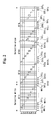
- FIG. 2 is a schematic diagram showing a plasma display panel (PDP) driving method according to a first exemplary embodiment of the present invention.
- PDP plasma display panel
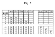
- FIG. 3 is a diagram showing a gray scale representation in the driving method of FIG. 2.
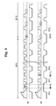
- FIG. 4 is a driving waveform diagram of the plasma display device according to exemplary embodiments of the present invention.
- FIG. 5 is a schematic diagram showing a PDP driving method according to a second exemplary embodiment of the present invention.
- FIG. 6 is a diagram showing a gray scale representation in the driving method of FIG. 5.
- FIG. 7 and FIG. 8 are schematic diagrams showing PDP driving methods according to third and fourth exemplary embodiments of the present invention, respectively.
- FIG. 1 is a schematic conceptual diagram showing a plasma display device according to an exemplary embodiment of the present invention.
- a plasma display device includes a plasma display panel (PDP) 100, a controller 200, an address electrode driver 300, a scan electrode (Y electrode) driver 400, and a sustain electrode (X electrode) driver 500.
- PDP plasma display panel
- controller 200 an address electrode driver 300, a scan electrode (Y electrode) driver 400, and a sustain electrode (X electrode) driver 500.
- the PDP 100 includes a plurality of address electrodes (A electrodes) A1 to Am extending in a column direction, and a plurality of X electrodes X1 to Xn and a plurality of Y electrodes Y1 to Yn, which extend in a row direction and are paired.
- the X electrodes X1 to Xn are formed corresponding to the Y electrodes Y1 to Yn.
- the A electrodes A1 to Am are arranged substantially perpendicular to the Y electrodes Y1 to Yn and the X electrodes X1 to Xn.
- a discharge space at an intersection of an A electrode and an X and Y electrode pair forms a discharge cell.
- Embodiments of the present invention may be applied to PDPs having other structures.
- one discharge cell is defined by a pair of X and Y electrodes and one A electrode. Additionally, a pair of X and Y electrodes, which extend in the row direction, is referred to as the row electrode, and the A electrode, which extends in the column direction, is referred to as the column electrode.
- the controller 200 receives a video signal, outputs driving control signals, divides one field into a plurality of subfields and drives the plurality of subfields.
- the A, Y and X electrode drivers 300, 400 and 500 apply driving voltages to the A electrodes A1 to Am, the Y electrodes Y1 to Yn, and the X electrodes X1 to Xn, respectively.
- FIG. 2 is a schematic diagram showing a PDP driving method according to a first exemplary embodiment of the present invention
- FIG. 3 is a diagram showing a gray scale representation in the driving method of FIG. 2.
- FIG. 2 shows, it is assumed that one TV field is divided into a plurality of equally weighted subfields SF11 to SF1L. Additionally, a plurality of row electrodes X1 to Xn and Y1 to Yn are divided into a plurality of row groups.
- a subfield includes an address period during which discharge cells to be lit and discharge cells not to be lit are selected from a plurality of discharge cells formed in the PDP 100 and a sustain period during which a sustain discharge operation, i.e., a display operation, is performed in a selected discharge cell during a period corresponding to a weight of a subfield.
- sustain discharge occurs when the sum of a wall voltage set between the X electrode and the Y electrode in the address period and a voltage applied between the X electrode and the Y electrode in the sustain period exceeds a discharge start voltage. The voltage applied between the X and Y electrodes in the sustain period is less than the discharge start voltage.
- Processes of selecting the light-emitting discharge cells and the non-light-emitting discharge cells in the address period include a selective write process and a selective erase process.
- the selective write process selects light-emitting discharge cells and forms a wall voltage on the selected light-emitting discharge cells.
- the selective erase process selects the non-light-emitting discharge cells by erasing a wall voltage, which was formed on the non-light-emitting discharge cell.
- a state where a light-emitting discharge cell is selected in the address period by the selective write process or not selected by the selective erase process is referred to as "a light-emitting cell state”
- a state where a non-light-emitting discharge cell is not selected in the address period by the selective write process or is selected in the selective erase process is referred to as "a non-light-emitting cell state.”
- erase, erased, and erasing do not necessarily require removal of all traces of the thing being erased.
- a discharge cell in the non-light-emitting state is set to the light-emitting cell state by write-discharging the discharge cell to form wall charges on the discharge cell.
- the selective write process is performed to select the discharge cell to be turned on.
- a discharge cell in the non-light-emitting state is set to the non-light-emitting cell state by erase-discharging the discharge cell to erase wall charges from the discharge cell.
- the selective erase process is performed to select a cell to be turned off.
- the address periods are sequentially performed for the plurality of row groups G 1 to G 8 in the plurality of subfields SF11 to SF1L, and sustain periods having the same length are performed between the address periods.
- the sum of an address period and a sustain period for one row group in each subfield is referred to as "a select period" of the row group
- the sum of sustain periods of all row groups in each subfield is referred to as "a display period" of the subfield. If the plurality of row electrodes consists of 8 row groups G 1 to G 8 as shown in FIG. 2, the display period is 8 times the sustain period in the select period of one row group.
- the first subfield SF11 has a reset period R11 during which the discharge cells of all row groups G 1 to G 8 are initialized to be non-light-emitting cells and are set to a state where the selective write operation may be successfully performed in the address period.
- Select periods for the first to eighth row groups G 1 to G 8 are then sequentially performed in the first subfield SF11.
- Light-emitting cells of the discharge cells of an i th row group G i are selected by write-discharging the cells in an address period WA11 i of the select period for the i th row group.
- a sustain discharge occurs in discharge cells of the light-emitting cell state of the i th row group G i , in a sustain period S11 i of the select period for the i th row group G i .
- the sustain discharge also occurs in discharge cells set to the light emitting cell state in each address period WA11 i for the first to (i-1) th row groups G 1 to G i-1 .
- the discharge cells of the i th row group G i set to the light-emitting cell state in the first subfield SF11 are sustain-discharged during sustain periods S11 i to S11 8 and S12 1 to S12 i-1 of each row group until the following select period for the i th row group G i of the second subfield SF12, i.e., during the display period.
- the select periods of the first to eighth row group G 1 to G 8 are sequentially performed in the second subfield SF12.
- Non-light-emitting cells of the discharge cells that were previously set to the light emitting cell state in the first subfield SF11 through the write discharge are selected in an address period EA12 i of the select period for the i th row group G i through the erase discharge.
- sustain discharge occurs for discharge cells of the light-emitting cell state (i.e., discharge cells not selected by the erase discharge that were previously selected as the light-emitting cells in the first subfield SF11).
- the sustain discharge also occurs in discharge cells, which are set to the light-emitting cell state in the second subfield SF12, of the discharge cells of the first to (i-1) th row groups G 1 to G i-1 and discharge cells, which are set to the light-emitting cell state in the first subfield SF11, of the discharge cells of the (i+1) th to eighth row groups G i+1 to G 8 .
- the discharge cells set to the light-emitting cell state in the i th row group G i are sustain-discharged until the following select period of the i th row group G i of the third subfield SF13, i.e., during the display period (S12 i to S12 8 and S13 1 to S13 i-1 ).
- the address period of the selective erase process and the sustain period are also sequentially performed for the first to eighth row groups G 1 to G 8 in the third to last subfields SF13 to SF1L.
- the discharge cells which are set to the light-emitting cell state through the write-discharge in the first subfield SF11, of the discharge cells of the i th row group G i , are sustain-discharged during the display period of each subfield until they are set to the non-light-emitting cell state through the erase discharge in an address period EA12 i to EA1L i of the subsequent subfields SF12 to SF1L. Then, when a discharge cell is set to the non-light-emitting cell state, the discharge cell is no longer sustain discharged from the corresponding subfield in which it was set to the non-light-emitting cell state until at least the next TV field.
- erase periods ER1 1 to ER1 8 are sequentially performed for the row groups G 1 to G 8 in the last subfield SF1 L. Since the first to eighth row group G 1 to G 8 perform the sustain discharge during the display period, the last subfield SF1L includes seven additional sustain periods SA1 2 to SA1 8 for the second to eighth row groups G 2 to G 8 , respectively. Without the erase periods ER1 1 to ER1 7 , the sustain discharge may be performed for row groups G 1 to G 7 for more than the display period. Accordingly, in the last subfield SF1L, erase processes are sequentially performed for the row groups G 1 to G 8 after the display period ends. These erase processes may be performed for all discharge cells of a corresponding row group, unlike the selective erase process of an address period as described above. Since the reset period R11 is performed in the first subfield SF11, the last erase period ER1 8 may be omitted.
- all discharge cells are set to the non-light-emitting cell state in the reset period R11.
- the non-light-emitting cell state is maintained in the address period WA11 i of the first subfield SF11, a gray scale level of 0 is represented since the sustain discharge does not occur in the sustain period. Further, the sustain discharge does not occur in the subsequent subfields SF12 to SF1 L.
- a gray scale level of 1 can be represented since the sustain discharge occurs in the display period of the subfield SF11.
- a final gray scale level of 1 is represented since the sustain discharge does not occur from the second subfield SF12 on.
- a gray scale level of 2 is represented because the sustain discharge also occurs in the sustain period of the second subfield SF12.
- a gray scale level of (k-1) is finally represented when the discharge cells are set to the light-emitting cell state through the write discharge occurring in the first subfield SF11 and then are set to the non-light-emitting cell state through the erase discharge in the k th subfield SF1k.
- these discharge cells are sustain-discharged in the first to (k-1) th subfields SF11 to SF1(k-1).
- FIG. 4 is a driving waveform diagram of the plasma display device according to exemplary embodiments of the present invention.
- FIG. 4 for convenience of explanation, only the first and second row groups G1 and G2 and the first and second subfields SF11 and SF12 are partially shown, and the A electrode is omitted. Additionally, since the driving waveform shown in FIG. 4 is a typical PDP driving waveform, detailed explanation thereof will be omitted.
- FIG. 4 shows, in the reset period R11 of the first subfield SF11, wall charges are formed in the discharge cells by reset discharge caused by gradually increasing a voltage of the Y electrodes of both row groups G 1 and G 2 while biasing the X electrodes at a ground voltage.
- the discharge cells are initialized by erasing the wall charges formed by the reset discharge by gradually decreasing the voltage of the Y electrodes of the row groups G 1 and G 2 while biasing the X electrodes at a positive voltage.
- a scan pulse (the ground voltage in FIG. 4) is sequentially applied to the Y electrodes of the first row group G 1 , and, although not shown, a positive address voltage is applied to the A electrode of discharge cells to be lit of the discharge cells corresponding to the Y electrode to which the scan pulse is applied. Then, the write discharge occurs in the discharge cells to which a voltage of the scan pulse and the address voltage are applied, thereby forming wall charges on the X electrode and the Y electrode. At this time, the scan pulse is not applied to Y electrodes of the second to eighth row groups G 2 to G 8 .
- a sustain discharge pulse is applied to the Y electrodes in order to discharge the discharge cells of the light-emitting cell state, and then, the sustain discharge pulse is applied to the X electrodes in order to discharge the discharge cells. Then, the scan pulse is sequentially applied to the Y electrodes of the second row group G 2 while applying the sustain discharge pulse to the X electrodes, thereby performing the address period of the second group G 2 . Next, the sustain discharge pulse is applied to the Y and X electrodes. In this manner, the select period for the first to eighth row groups G 1 to G 8 is performed in the first subfield SF11.
- a scan pulse having a negative voltage is sequentially applied to the Y electrodes of the first row group G 1 , and then, a positive voltage (not shown) is applied to the A electrode of the discharge cells to be set to the non-light-emitting cell state.
- a positive voltage (not shown) is applied to the A electrode of the discharge cells to be set to the non-light-emitting cell state.
- the narrow width of the scan pulse causes an address discharge that erases, rather than forms, wall charges.
- the address periods are formed between the sustain periods of the row groups, priming particles formed in the sustain periods may be sufficiently utilized in the address periods.
- high speed scanning with a narrow scan pulse may be achieved.
- the width of the scan pulse may be further narrowed to erase wall charges.
- gradually increasing and decreasing voltages are used in the reset period, a strong discharge does not occur, and since the reset period is performed once for all row groups during one field, the contrast ratio may be increased.
- the width of the scan pulse in the selective write process is 1.5 ⁇ s
- the width of the scan pulse in the selective erase process is 0.5 ⁇ s
- the length of the reset period is 350 ⁇ s
- 20 sustain discharge pulses having a width of 5 ⁇ s occur in one subfield.
- a total of 46 subfields may be accommodated in one subfield (16.6 ms), and 47 gray scale levels (i.e.
- FIG. 5 is a schematic diagram showing a PDP driving method according to the second exemplary embodiment of the present invention
- FIG. 6 is a diagram showing a gray scale representation in the driving method of FIG. 5.
- the plurality of subfields SF21 to SF2L is grouped into two groups of subfields.
- the first group of subfields includes at least the first subfield of the subfields
- the second group of subfields includes the remaining subfields.
- FIG. 5 shows the first group of subfields including the first to third subfields SF21, SF22 and SF23 and the second group of subfields including the remaining subfields SF24 to SF2L.
- the plurality of row electrodes is divided into the plurality of row groups G 1 to G 8 .
- the first group of subfields SF21 to SF23 have respective weights, and gray scales are represented by a combination of the weights of the subfields SF21 to SF23.
- the second group of subfields SF24 to SF2L represent gray scales in the same manner as the subfields SF11 to SF1L described in the first exemplary embodiment.
- the address periods of the selective write process are sequentially performed in the first group of subfields SF21 to SF23 and the sustain periods are performed after the address periods. Additionally, the subfields SF21, SF22 and SF23 begin with reset periods R21, R22 and R23, respectively. In the reset periods R21, R22, and R23, all discharge cells are initialized to be non-light-emitting cells and are set to a state where the selective write operation may be performed in the following address periods.
- a reset period R2k is performed in a k th subfield SF2k of the first group subfields (where, according to the embodiment of FIG. 5, k is 1, 2 or 3).
- select periods are sequentially performed for the first to eighth row groups G 1 to G 8 .
- Light-emitting cells are selected from the discharge cells of the i th row group G i through the write discharge in an address period WA2k i of the select period for the i th row group G i .
- Sustain discharge occurs in the discharge cells of the light-emitting cell state of the i th row group G i , in a sustain period S2k i of the select period for the i th row group G i .
- an erase operation is performed to erase the wall charges of the discharge cells of the i th row group G i at the end of the sustain period S2k i . Accordingly, the discharge cells set to the light-emitting cell state in the i th row group G i emit light in the sustain period S2k i of the select period for the i th row group G i , but they do not emit light in a select period for the next row group G i+1 . Therefore, since the discharge cells set to the light-emitting cell state in each row group G i emit light in only their own select periods, the weight of the k th subfield SF2k of the first group corresponds to the length of the sustain period S2k i of one row group.
- the sustain discharge may be selectively performed in each subfield for the discharge cells.
- the relative length (i.e., weight) of sustain periods S21 i to S23 i of the first to third subfields SF21 to SF23 is 1, 2 and 4, respectively, 8 gray scale levels (0 to 7) may be represented by the first group of subfields SF21 to SF23.
- the last pulse of the sustain discharge pulses of the sustain period S2k i may be narrower than the previous pulses so that wall charges are not formed.
- the wall charges formed by the sustain discharge may be erased by using a waveform that gradually changes voltages of the row electrodes after the last sustain discharge pulse.
- the subfields in the second group of subfields SF24 to SF2L has the same structure as the subfields SF11 to SF1L described in the first exemplary embodiment. That is, the address period and the sustain period are sequentially performed for the plurality of row groups G 1 to G 8 .
- a first subfield SF24 of the second group of subfields has the reset period R24 like the subfield SF11 of the first exemplary embodiment
- the select period of each row group Gi includes the address period WA24 i of the selective write process and the sustain period S24 i .
- the select period of each row group Gi in the remaining subfields SF25 to SF2L of the second group of subfields has the address periods EA25 i to EA2L i of the selective erase process and the sustain period S25 i to S2L i , like the select period for each row group Gi in the subfields SF12 to SF1L in the first exemplary embodiment.
- the last subfield SF2L has erase periods ER2 1 to ER2 8 and additional sustain periods SA 2 to SA 8 like the last subfield SF1 L in the first exemplary embodiment. However, since the reset period R21 is performed in the first subfield SF21, the last erase period ER2 8 may be omitted.
- display periods each of which is the sum of sustain periods of subfields in the second group of subfields, have the same length. Furthermore, the display periods are equal to the length of the sustain period S21 i of the first subfield SF21 plus the sum of the lengths of the sustain periods S21 i to S23 i of the first group of subfields SF21 to SF23. That is, each subfield of the second group of subfields has a display period that may represent a gray scale level that is one more than the maximum gray scale level that may be represented by the first group of subfields SF21 to SF23.
- the display periods of the second group of subfields may represent a gray scale level of 8. Since the display period of the second group of subfields is eight times the sustain period S25i to S2L i of each row group, the length of the sustain period S25i to S2L i may be equal to the length of the sustain period of the first subfield S21 i .
- gray scales may be represented by the sum of display periods of successive subfields starting from the fourth subfield SF24. Further, gray scales within one field may be represented by the sum of gray scales represented in the first group of subfields SF21 to SF23 and gray scales represented in the second group of subfields SF24 to SF2L. Now, a method of such a gray scale representation will be described in detail with reference to FIG. 6.
- SW represents that a discharge cell is set to the light-emitting cell state through the write discharge occurring in a corresponding subfield
- SE represents that a discharge cell is set to the non-light-emitting cell state through the erase discharge occurring in a corresponding subfield
- ⁇ represents a discharge cell that maintains the light-emitting cell state in a corresponding subfield.
- gray scale levels of 0 to 7 are represented by a combination of subfields lighted in the first group of subfields SF21 to SF23. Additionally, gray scale levels that are multiples of 8 are represented by subfields successively lighted in the second group of subfields SF24 to SF2L, and gray scale levels that are greater than 8, but are not multiples of 8, are represented by a combination of the first group of subfields SF21 to SF23 and the second group of subfields SF24 to SF2L.
- a gray scale level of 8N (where N is an integer) is represented by the second group of subfields. That is, the gray scale level of 8N is represented when the non-light-emitting cell state is set through the erase discharge in an (N+1) th subfield SF2(N+4) of the second group of subfields after the light-emitting cell state is set at the subfield SF24 through the write discharge.
- the gray scale level of 5 is represented in the first group of subfields. Accordingly, a total gray scale level of (8N + 5) is represented in the first and second groups of subfields.
- gray scale levels of 0 to 255 can be represented by a combination of the 34 total subfields. Accordingly, the number of subfields may be reduced as compared to the first exemplary embodiment.
- FIG. 7 is a schematic diagram showing a driving method of a plasma display according to the third exemplary embodiment of the present invention.
- the plurality of subfields has the same structure as the second exemplary embodiment except the first group of subfields SF31 to SF33.
- display periods are controlled by the number of row groups.
- a structure and driving method of the second group of subfields SF34 to SF3L is the same as that of the second group of subfields SF24 to SF2L in the second exemplary embodiment. More specifically, a first subfield SF34 of the second group of subfields, which is the fourth subfield of all the subfields in FIG. 7, has a reset period R34, address periods WA34 1 to WA34 8 of the selective write process, and sustain periods S34 1 to S34 8 for each row group G 1 to G 8 .
- a k th subfield SF3k in the second group of subfields has address periods EA3k 1 to EA3k 8 of the selective erase process and sustain periods S3k 1 to S3k 8 for each row group G 1 to G 8 (where, k is an integer from 5 to L). Additionally, the last subfield SF3L has erase periods ER3 1 to ER3 8 for each row group G 1 to G 8 and additional sustain periods SA3 2 to SA3 8 for each of the second to eighth row group G 2 to G 8 .
- the number of row groups (4) in the third subfield SF33 of the first group of subfields SF31 to SF33 is 1/2 the number of row groups (8) in the second group of subfields SF34 to SF3L.
- the number of row groups (2) in the second subfield SF32 is 1/4 the number of row groups (8) in the second group of subfields SF34 to SF3L.
- the number of row groups (1) in the first subfield SF31 is 1/8 the number of row groups (8) in the second group of subfields SF34 to SF3L.
- the first group of subfields SF31, SF32 and SF33 begin with reset periods R31, R32 and R33, respectively.
- the reset periods R31, R32, and R33 all discharge cells are initialized to be non-light-emitting cells and are set to a state where the selective write operation may be performed in the following address periods.
- the address periods of the selective write process are sequentially performed for the row groups in the first group of subfields SF31 to SF33.
- the reset period R31 is performed in the first subfield SF31 of the first group of subfields SF31 to SF33.
- the address period WA31 is performed for the plurality of row electrodes to thereby select light-emitting cells of the plurality of row electrodes.
- the sustain period S31 is performed so that the sustain discharge occurs in discharge cells of the light-emitting cell state.
- the length of the sustain period S31 equals the length of the sustain period of the select period for one row group in the second group of subfields. That is, the brightness in the first subfield SF31 is 1/8 the brightness in a subfield of the second group of subfields.
- the reset periods R32 and R33 are performed to initialize the state of the discharge cells, and then the select periods are sequentially performed for each row group. After the select periods of each row group ends, an erase period and additional sustain periods are sequentially performed.
- the second subfield SF32 comprises a first row group G 1 to G 4 and a second row group G 5 to G 8
- the address period WA32 1 and the sustain period S32 1 are performed for the first row group G 1 to G 4
- the address period WA32 2 and the sustain period S32 2 are performed for the second row group G 5 to G 8
- the erase period ER32 1 is performed for the first row group G 1 to G 4 , thereby setting the discharge cells of the first row group G 1 to G 4 to the non-light-emitting state
- an additional sustain period SA32 2 is performed to thereby generate the sustain discharge in the second row group G 5 to G 8 .
- the erase period ER32 2 is performed to set the discharge cells of the second row group G 5 to G 8 to the non-light-emitting state.
- the reset period R33 starts the third subfield SF33, the erase period ER32 2 may be omitted.
- each sustain period S32 1 , S32 2 and SA32 2 equals the length of the sustain period of the select period for one row group in the second group of subfields.
- two sustain periods are performed for each row group in the second subfield SF32.
- the brightness in the second subfield SF32 is 1/4 the brightness in a subfield of the second group of subfields.
- the third subfield SF33 comprises four row groups (G 1 and G 2 ), (G 3 and G 4 ), (G 5 and G 6 ), and (G 7 and G 8 ), the select periods of the first to fourth groups of subfields are sequentially performed. That is, the address period WA33 i and the sustain period S33 i are performed for the i th row group G 2i-1 to G 2i .
- erase periods ER33 1 , ER33 2 , ER33 3 , ER33 4 are sequentially performed for each row group (G 1 and G 2 ), (G 3 and G 4 ), (G 5 and G 6 ), and (G 7 and G 8 ), and additional sustain periods SA33 2 , SA33 3 , SA33 4 are inserted between the erase periods. Accordingly, four sustain periods are performed for each row group. However, since the reset period R34 is performed in the fourth subfield SF34, the last erase period ER32 4 may be omitted.
- each sustain period S33 1 to S33 4 and SA33 2 to SA33 4 equals the length of the sustain period of the select period for one row group in the second group of subfields.
- four sustain periods are performed for each row group in the third subfield SF33.
- the brightness in the third subfield SF33 is 1/2 of the brightness in a subfield in the second group of subfields.
- discharge cells may be set to the light-emitting cell state irrespective of the their state in a previous subfield.
- the weight of each subfield in the second group of subfields is 8
- the weights of the first to third subfields SF31 to SF33 are 1, 2 and 4, respectively, 8 gray scale levels (0 to 7) may be represented by a combination of the first group of subfields SF31 to SF33, like the second exemplary embodiment.
- the third exemplary embodiment like the second exemplary embodiment, when the second group of subfields SF34 to SF3L includes 31 total subfields and the first group of subfields SF31 to SF33 includes 3 total subfields, 256 gray scale levels (0 to 255) may be represented. Accordingly, the number of subfields may be reduced as compared to the first exemplary embodiment.
- the number of row groups determines the weights of the subfields.
- the sustain discharge occurs after sequentially performing the selective write discharge for all row electrodes.
- the sustain discharge may not smoothly occur due to loss of wall charges formed by the selective write discharge or loss of priming particles of the discharge cells.
- FIG. 8 is a schematic diagram showing a driving method of a plasma display according to a fourth exemplary embodiment of the present invention.
- the plurality of subfields has the same structure as the third exemplary embodiment except for the first subfield SF41. That is, a structure and driving method of second and third subfields SF42 and SF43 of a first group of subfields and a second group of subfields SF44 and SF4L is the same as that of the second and third subfields SF32 and SF33 and the second group of subfields SF34 to SF3L of FIG. 7.
- the first subfield SF41 includes a reset period R41 to initialize the discharge cells.
- Light-emitting cells are set for a first row group G 1 to G 4 in an address period WA41 1 of the selective write process, and then sustain discharge occurs in the light-emitting cells of the first row group G 1 to G 4 in a sustain period S41 1 .
- An erase operation for erasing wall charges of the discharge cells is performed at the end of the sustain period S41 1 .
- light-emitting cells are set for a second row group G 5 to G 8 in an address period WA41 2 of the selective write process, and then the sustain discharge occurs in the light-emitting cells of the second row group G 5 to G 8 in a sustain period S41 2 .
- the erase operation for erasing wall charges of the discharge cells may be performed at the end of the sustain period S41 2 .
- the erase operation may be omitted since a reset period R42 is performed in the next subfield SF42.
- reset periods R42 and R43, address periods WA42 1 , WA42 2 , WA43 1 to WA43 4 , sustain periods S42 1 , S42 2 , SA42 2 , S43 1 to S42 4 , and SA43 2 to SA43 4 , and erase periods ER42 1 , ER42 2 , ER43 1 to ER43 4 in the remaining subfields SF42 and SF43 of the first group of subfields are the same as reset periods R32 and R33, address periods WA32 1 , WA32 2 , WA33 1 to WA33 4 , sustain periods S32 1 , S32 2 , SA32 2 , S33 1 to S32 4 , and SA33 2 to SA33 4 , and erase periods ER32 1 , ER32 2 , ER33 1 to ER33 4 in the remaining subfields SF32 and SF33 of the first group of subfields in the third exemplary embodiment, respectively.
- a reset period R44, address periods WA44 i and EA4k i , sustain periods S4k i and SA4k j , and an erase period ER4L i in the second group of subfields SF44 to SF4L are the same as the reset period R34, the address periods WA33 i and EA3k i , the sustain periods S3k i and SA3k j , and the erase period ER3L i in the second group of subfields SF34 to SF3L in the third exemplary embodiment, respectively (where, k is an integer from 4 to L, i is an integer from 1 to 8, and j is an integer from 2 to 8).
- the third and fourth exemplary embodiments differ in the grouping method of the row electrodes from the second exemplary embodiment. That is, in the third and fourth exemplary embodiments, the first group of subfields is divided into a group of subfields having minimal weights (the third group of subfields) and a group of the remaining subfields (the fourth group of subfields), and the row electrodes are grouped with the number of row electrodes corresponding to weights of relevant subfields in the fourth group of subfields. Similarly, in the third group of subfields, the row electrodes are grouped with the number of row electrodes corresponding to weights of relevant subfields (the third exemplary embodiment), or with the more number row electrodes (the fourth exemplary embodiment).
- gray scales may be represented by the number of subfields successively lighted without using subfields having large weights, the problem of false contour may be overcome.
- the addressing operation is performed for each row group after the sustain period, priming particles produced during the sustain period may be used for the address discharge, thus reducing the width of the scan pulse.
- the width of the scan pulse may be further reduced by using the address period of the selective erase process, it is possible to achieve high speed scanning.
Landscapes
- Engineering & Computer Science (AREA)
- Physics & Mathematics (AREA)
- Power Engineering (AREA)
- Plasma & Fusion (AREA)
- Computer Hardware Design (AREA)
- General Physics & Mathematics (AREA)
- Theoretical Computer Science (AREA)
- Control Of Indicators Other Than Cathode Ray Tubes (AREA)
- Control Of Gas Discharge Display Tubes (AREA)
- Transforming Electric Information Into Light Information (AREA)
Abstract
Description
- The present invention relates to a display device and a driving method thereof, and more particularly, to a driving method for representing gray scales using subfields.
- Generally, in a display device such as a plasma display, one field (1TV field) is divided into a plurality of subfields, and each subfield has an assigned weight. Gray scales are represented by combining weights of active (i.e., displayed) subfields of the plurality of subfields. Each subfield typically includes an address period, during which discharge cells to be lit are selected, and a sustain period, during which the selected discharge cells are sustain discharged during a period corresponding to the subfield's weight.
- An address display separation (ADS) driving method includes performing a sustain discharge operation for all discharge cells after addressing all discharge cells in each subfield. In other words, the address period is separate from the sustain period. The ADS method can be easily implemented, but since the addressing operation is sequentially performed for all discharge cells, some discharge cells to be addressed in the latter stages of the address period may not actually get addressed due to lack of priming particles within the discharge cells. Therefore, to secure a stable addressing operation, the width of scan pulses sequentially applied to row electrodes may be increased, but this lengthens the address period. Consequently, the subfields also become longer, which limits the number of subfields available in one field.
- Unlike the ADS method, an address while display (AWD) driving method includes inserting an address pulse for each line between two successive sustain discharge pulses and performing the addressing operation for one line while performing the sustain discharge operation for another line. Hence, with this method, the address period is not separate from the sustain period.
- In the AWD method, a relatively lengthy reset pulse is inserted between an address pulse and a sustain discharge pulse. In other words, a strong reset discharge may cause a black screen to be seen brightly, thereby deteriorating contrast ratio.
- Additionally, both the ADS method and the AWD method may use different weighted subfields to represent gray scales. For example, with subfields having weights of a type of the second power of 2, a so-called false contour may be produced when one discharge cell represents a 127th gray scale level in one frame and a 128th gray scale level in a following frame.
- The present invention provides a driving method of a display device, which is capable of performing a high speed scan operation.
- The present invention also provides a driving method of a display device, which is capable of reducing false contour.
- The present invention also provides a driving method of a display device, which is capable of improving contrast ratio.
- The present invention also provides a driving method of grouping a plurality of subfields into groups of subfields for setting light-emitting cells through write discharge and groups of subfields for setting non-light-emitting cells through erase discharge after setting the light-emitting cells through the write discharge.
- Additional features of the invention will be set forth in the description which follows, and in part will be apparent from the description, or may be learned by practice of the invention.
- The present invention discloses a driving method of dividing one field into a plurality of subfields and representing a gray scale using the plurality of subfields in a display device including a plurality of row electrodes, a plurality of column electrodes intersecting the plurality of row electrodes, and a plurality of discharge cells defined by the plurality of row electrodes and the plurality of column electrodes. The plurality of row electrodes is grouped into a plurality of row groups, each subfield is divided into a plurality of select periods respectively corresponding to the plurality of row groups, and the plurality of subfields is grouped into a plurality of subfield groups. In a select period for a first row group of a first group of subfields, light-emitting cells are selected from discharge cells of the first row group, and the light-emitting cells of the first row group are set to non-light-emitting cells after the light-emitting cells are sustain-discharged during a sustain period. In a select period for the first row group of a first subfield, which is positioned at the head in time, of a second group of subfields, light-emitting cells are selected from discharge cells of the first row group and the light-emitting cells are sustain-discharged during a sustain period. In a select period for the first row group of a second subfield of the second group of subfields, non-light-emitting cells are selected from the light-emitting cells of the first row group and remaining light-emitting cells are sustain-discharged during a sustain period.
- The present invention also discloses a driving method of dividing one field into a plurality of subfields and representing a gray scale using the plurality of subfields in a display device including a plurality of row electrodes, a plurality of column electrodes intersecting the plurality of row electrodes, and a plurality of discharge cells defined by the plurality of row electrodes and the plurality of column electrodes. The plurality of subfields is grouped into a first group of subfields including a minimal weight subfield, a second group of subfields, and a third group of subfields including at least two consecutive subfields. Additionally, the plurality of row electrodes is grouped into a plurality of row groups in the third group of subfields, and the plurality of row electrodes is grouped into a number of row groups corresponding to a weight of a subfield for each subfield in the second group of subfields. In the second and third groups of subfields, each subfield is divided into a plurality of select periods respectively corresponding to the plurality of row groups. In the first group of subfield, light-emitting cells are selected in the plurality of row electrodes, and the light-emitting cells are discharged during a period corresponding to a weight of a corresponding subfield. In a select period for a first row group of the second group of subfields, light-emitting cells are selected from discharge cells of the first row group, and the light-emitting cells are discharged during a sustain period. In a select period for a second row group of a first subfield, which is positioned at the head in time, of the third group of subfields, light-emitting cells are selected from discharge cells of the second row group, and the light-emitting cells are discharged during a sustain period. In a select period for the second row group of a second subfield of the third group of subfields, non-light-emitting cells are selected from the light-emitting cells of the second row group, and remaining light-emitting cells are discharged during a sustain period.
Preferably the method further comprises: in a select period for a third row group of the second group of subfields, light-emitting cells from discharge cells of the third row group are selected and the light-emitting cells of the third row group during a sustain period are discharged; in a select period for a fourth row group of the first subfield, light-emitting cells from discharge cells of the fourth row group are selected and the light-emitting cells of the fourth row group during a sustain period are discharged; and in a select period for the fourth row group of the second subfield, non-light-emitting cells from the light-emitting cells of the fourth row group are selected and remaining light-emitting cells of the fourth row group during a sustain period are discharged. Preferably in the third group of subfields, light-emitting cells of the second row group are discharged during a sustain period of a select period for the fourth row group. Preferably in the third group of subfields, a length of a sustain period of a select period for the second row group is equal to a length of the sustain period of the select period for the fourth row group. Preferably in the second group of subfields, the light-emitting cells of the first row group are set to non-light-emitting cells after a specific period elapses. Preferably the specific period is a period during which sustain discharge for a period corresponding to a weight of a corresponding subfield of the first row group is completed. After the light-emitting cells of the first row group are set to the non-light-emitting cells, preferably a sustain period is performed for the light-emitting cells of the third row group.
Preferably in the minimal weight subfield, sustain discharge is performed after selecting light-emitting cells for all row electrodes. Preferably in the minimal weight subfield, the plurality of row electrodes is grouped into at least two row groups, and the wherein discharging the light-emitting cells during the period corresponding to the weight of the corresponding subfield includes: selecting light-emitting cells for a fifth row group of the at least two row groups and setting the light-emitting cells of the fifth row group to non-light-emitting cells after sustain-discharging the light-emitting cells of the fifth row group during a sustain period; and selecting light-emitting cells for a sixth row group of the at least two row groups and setting the light-emitting cells of the sixth row group to non-light-emitting cells after sustain-discharging the light-emitting cells of the sixth row group during a sustain period.
Preferably a gray scale level represented in the first group of subfields and the second group of subfields is determined by a sum of the weights of subfields in which a discharge cell is selected to be a light-emitting cell. Preferably, when the discharge cell is selected to be a light-emitting cell in the first subfield and then is selected to be a non-light-emitting cell in an nth subfield of the third group of subfields, a gray scale level represented in the third group of subfields is determined by a sum of weights of (n-1) subfields of the third group of subfields. Preferably all subfields of the third group of subfields have the same weight. Preferably a total sum of weights of all subfields of the first group of subfields and the second group of subfields is one less than a weight of one subfield of the third group of subfields. Preferably the first group of subfields, the second group of subfields, and the first subfield respectively include a reset period during which the plurality of discharge cells are initialized to be non-light-emitting cells. Preferably in a third subfield, which is a last subfield in time of the third group of subfields, light-emitting cells of the second row group are set to non-light-emitting cells after a specific period elapses. Preferably the specific period is a period during which sustain discharge for a period corresponding to a weight of a corresponding subfield of the second row group is completed. Preferably, after the light-emitting cells of the second row group are set to the non-light-emitting cells, a sustain period is performed for the light-emitting cells of the fourth row group. - The present invention also discloses a driving method of dividing one field into a plurality of subfields and representing a gray scale using the plurality of subfields in a display device including a plurality of row electrodes, a plurality of column electrodes intersecting the plurality of row electrodes, and a plurality of discharge cells defined by the plurality of row electrodes and the plurality of column electrodes. The plurality of row electrodes is grouped into a plurality of row groups, and the plurality of subfields is grouped into a plurality of subfield groups. In each subfield of a first group of subfields, light-emitting cells for each row group are sequentially set. In each subfield of the first group of subfields, the light-emitting cells of the each row group are set to non-light-emitting cells after the light-emitting cells are sustain-discharged during a first period between a period for setting the light-emitting cells of a row group and a period for setting light-emitting cells of a next row group. In each subfield of a second group of subfields, light-emitting cells for each row group are sequentially set. In each subfield of the second group of subfields, the light-emitting cells are sustain-discharged during a second period between a period for setting the light-emitting cells of a row group and a period for setting light-emitting cells of a next row group.
Preferably the first group of subfields performs a first type address discharge, the second group of subfields includes a subfield for performing the first type address discharge and a subfield for performing a second type address discharge, and a non-light-emitting cell is selected to be a light-emitting cell by the first type address discharge and the light-emitting cell is selected to be the non-light-emitting cell by the second type address discharge. Preferably the subfield for performing the first type address discharge in the second group of subfields is positioned at the head in time in the second group of subfields. Preferably the first group of subfields includes a plurality of subfields having respective weights, and a length of the first period for each subfield of the first group of subfields corresponds to a weight of each subfield of the first group of subfields. Preferably the second period is repeated for each row group by a number of row groups in the second group of subfields. - The present invention also discloses a driving method of dividing one field into a plurality of subfields and representing a gray scale using the plurality of subfields in a display device including a plurality of row electrodes, a plurality of column electrodes intersecting the plurality of row electrodes, and a plurality of discharge cells defined by the plurality of row electrodes and the plurality of column electrodes. In each subfield of a first group of subfields including a minimal weight subfield of the plurality of subfields, light-emitting cells are set in the plurality of row electrodes, and the light-emitting cells are sustain-discharged during a period corresponding to a weight of the corresponding subfield. In each subfield of a second group of subfields of the plurality of subfields, the plurality of row electrodes is grouped into a number of row groups corresponding to a weight of the corresponding subfield, and light-emitting cells for each of the row groups are sequentially set. In each subfield of the second group of subfields, the light-emitting cells are sustain-discharged during a first period between a period for setting the light-emitting cells of a row group and a period for setting light-emitting cells of a next row group. In each subfield of a third group of subfields of the plurality of subfields, the plurality of row electrodes is grouped into a plurality of row groups, and light-emitting cells for each of the row groups are sequentially set. In each subfield of the third group of subfields, the light-emitting cells are sustain-discharged during a second period between a period for setting the light-emitting cells of a row group and a period for setting light-emitting cells of a next row group.
Preferably the first group of subfields and the second group of subfields perform a first type address discharge, the third group of subfields includes a subfield for performing the first type address discharge and a subfield for performing a second type address discharge, and a non-light-emitting cell is selected to be a light-emitting cell by the first type address discharge and the light-emitting cell is selected to be the non-light-emitting cell by the second type address discharge. Preferably the subfield for performing the first type address discharge in the third group of subfields is positioned at the head in time in the third group of subfields. Preferably the first period is repeated for each row group by weights of the subfields in the second group of subfields, and the second period is repeated for each row group by a number of the plurality of row groups in the third group of subfields. - The present invention also discloses a display device including a display panel including a plurality of row electrodes, a plurality of column electrodes intersecting the plurality of row electrodes, and a plurality of discharge cells defined by the plurality of row electrodes and the plurality of column electrodes, a driver for driving the display panel, and a controller for controlling the driver such that one field is divided into a plurality of subfields to represent a gray scale. The controller groups the plurality of subfields into a plurality of subfield groups including a first group of subfields including a minimal weight subfield and a second group of subfields including at least two consecutive subfields. In addition, the controller controls the driver to set a non-light-emitting cell to a light-emitting cell through discharge in subfields, which are positioned at the head in time, of the first and second groups of subfields. Furthermore, the controller controls the driver to set a light-emitting cell to a non-light-emitting cell through discharge in remaining subfields of the second group of subfields.
The present invention also discloses a driving method of dividing one field into a plurality of subfields and representing a gray scale using the plurality of subfields in a display device including a plurality of row electrodes, a plurality of column electrodes intersecting the plurality of row electrodes, and a plurality of discharge cells defined by the plurality of row electrodes and the plurality of column electrodes, the driving method comprising: grouping the plurality of subfields into a first group of subfields and a second group of subfields; in the first group of subfields, turning on a discharge cell to be lit in a subfield irregardless of the discharge cell's previous on/off state in a previous subfield; and in the second group of subfields, turning on a discharge cell to be lit only in a first subfield in time of the second group of subfields and turning off the discharge cell only in a subsequent subfield. - It is to be understood that both the foregoing general description and the following detailed description are exemplary and explanatory and are intended to provide further explanation of the invention as claimed.
- The accompanying drawings, which are included to provide a further understanding of the invention and are incorporated in and constitute a part of this specification, illustrate embodiments of the invention and together with the description serve to explain the principles of the invention.
- FIG. 1 is a schematic conceptual diagram showing a plasma display device according to an exemplary embodiment of the present invention.
- FIG. 2 is a schematic diagram showing a plasma display panel (PDP) driving method according to a first exemplary embodiment of the present invention.
- FIG. 3 is a diagram showing a gray scale representation in the driving method of FIG. 2.
- FIG. 4 is a driving waveform diagram of the plasma display device according to exemplary embodiments of the present invention.
- FIG. 5 is a schematic diagram showing a PDP driving method according to a second exemplary embodiment of the present invention.
- FIG. 6 is a diagram showing a gray scale representation in the driving method of FIG. 5.
- FIG. 7 and FIG. 8 are schematic diagrams showing PDP driving methods according to third and fourth exemplary embodiments of the present invention, respectively.
- In the following detailed description, exemplary embodiments of the present invention are shown and described, by way of illustration. As those skilled in the art would recognize, the described exemplary embodiments may be modified in various ways, all without departing from the spirit or scope of the present invention. Accordingly, the drawings and description are to be regarded as illustrative in nature, rather than restrictive. In the drawings, illustrations of elements having no relation with the present invention are omitted in order to prevent the subject matter of the present invention from being unclear. In the specification, the same or similar elements are denoted by the same reference numerals even though they are depicted in different drawings.
- Hereinafter, a display device and a driving method thereof according to exemplary embodiments of the present invention will be described in detail with reference to the accompanying drawings. A plasma display will be exemplified and described in the exemplary embodiments.
- FIG. 1 is a schematic conceptual diagram showing a plasma display device according to an exemplary embodiment of the present invention.
- As FIG. 1 shows, a plasma display device according to an exemplary embodiment of the present invention includes a plasma display panel (PDP) 100, a
controller 200, anaddress electrode driver 300, a scan electrode (Y electrode)driver 400, and a sustain electrode (X electrode)driver 500. - The
PDP 100 includes a plurality of address electrodes (A electrodes) A1 to Am extending in a column direction, and a plurality of X electrodes X1 to Xn and a plurality of Y electrodes Y1 to Yn, which extend in a row direction and are paired. Generally, the X electrodes X1 to Xn are formed corresponding to the Y electrodes Y1 to Yn. The A electrodes A1 to Am are arranged substantially perpendicular to the Y electrodes Y1 to Yn and the X electrodes X1 to Xn. Here, a discharge space at an intersection of an A electrode and an X and Y electrode pair forms a discharge cell. Embodiments of the present invention may be applied to PDPs having other structures. - In the following description, one discharge cell is defined by a pair of X and Y electrodes and one A electrode. Additionally, a pair of X and Y electrodes, which extend in the row direction, is referred to as the row electrode, and the A electrode, which extends in the column direction, is referred to as the column electrode.
- The
controller 200 receives a video signal, outputs driving control signals, divides one field into a plurality of subfields and drives the plurality of subfields. The A, Y andX electrode drivers - Next, a PDP driving method according to a first exemplary embodiment of the present invention will be described with reference to FIG. 2, FIG. 3 and FIG. 4. In the first exemplary embodiment of the present invention, it is assumed that the length of sustain periods following address periods of each row group are equal and that these sustain periods have the same length in all subfields.
- FIG. 2 is a schematic diagram showing a PDP driving method according to a first exemplary embodiment of the present invention, and FIG. 3 is a diagram showing a gray scale representation in the driving method of FIG. 2.
- As FIG. 2 shows, it is assumed that one TV field is divided into a plurality of equally weighted subfields SF11 to SF1L. Additionally, a plurality of row electrodes X1 to Xn and Y1 to Yn are divided into a plurality of row groups. For example, FIG. 2
shows 8 row groups G1 to G8 for convenience of explanation. That is, first to jth row electrodes are set as a first row group G1, (j+1)th to (2j)th row electrodes are set as a second row group G2, and, in this way, (7j+1)th to nth row electrodes are set as an eighth row group G8 (where j = n/8). - Generally, a subfield includes an address period during which discharge cells to be lit and discharge cells not to be lit are selected from a plurality of discharge cells formed in the
PDP 100 and a sustain period during which a sustain discharge operation, i.e., a display operation, is performed in a selected discharge cell during a period corresponding to a weight of a subfield.. Here, sustain discharge occurs when the sum of a wall voltage set between the X electrode and the Y electrode in the address period and a voltage applied between the X electrode and the Y electrode in the sustain period exceeds a discharge start voltage. The voltage applied between the X and Y electrodes in the sustain period is less than the discharge start voltage. - Processes of selecting the light-emitting discharge cells and the non-light-emitting discharge cells in the address period include a selective write process and a selective erase process. The selective write process selects light-emitting discharge cells and forms a wall voltage on the selected light-emitting discharge cells. The selective erase process selects the non-light-emitting discharge cells by erasing a wall voltage, which was formed on the non-light-emitting discharge cell. In the following description, a state where a light-emitting discharge cell is selected in the address period by the selective write process or not selected by the selective erase process is referred to as "a light-emitting cell state", and a state where a non-light-emitting discharge cell is not selected in the address period by the selective write process or is selected in the selective erase process is referred to as "a non-light-emitting cell state." Here, erase, erased, and erasing do not necessarily require removal of all traces of the thing being erased.
- In the first exemplary embodiment of the present invention, in an address period of a first subfield SF11, a discharge cell in the non-light-emitting state is set to the light-emitting cell state by write-discharging the discharge cell to form wall charges on the discharge cell. In other words, the selective write process is performed to select the discharge cell to be turned on. In address periods of the subfields SF12 to SF1L, a discharge cell in the non-light-emitting state is set to the non-light-emitting cell state by erase-discharging the discharge cell to erase wall charges from the discharge cell. In other words, the selective erase process is performed to select a cell to be turned off. Additionally, the address periods are sequentially performed for the plurality of row groups G1 to G8 in the plurality of subfields SF11 to SF1L, and sustain periods having the same length are performed between the address periods. In the following description, the sum of an address period and a sustain period for one row group in each subfield is referred to as "a select period" of the row group, and the sum of sustain periods of all row groups in each subfield is referred to as "a display period" of the subfield. If the plurality of row electrodes consists of 8 row groups G1 to G8 as shown in FIG. 2, the display period is 8 times the sustain period in the select period of one row group.
- Next, the driving method according to the first exemplary embodiment of the present invention will be described in detail with reference to FIG. 2.
- To start, all discharge cells are initialized to prevent discharge cells not selected in the first subfield SF11 from being erroneously discharged in the sustain period and to accurately perform the selective write process in the address period so that discharge cells to be lit are selected. Accordingly, the first subfield SF11 has a reset period R11 during which the discharge cells of all row groups G1 to G8 are initialized to be non-light-emitting cells and are set to a state where the selective write operation may be successfully performed in the address period.
- Select periods for the first to eighth row groups G1 to G8 are then sequentially performed in the first subfield SF11. Light-emitting cells of the discharge cells of an ith row group Gi are selected by write-discharging the cells in an address period WA11i of the select period for the ith row group. A sustain discharge occurs in discharge cells of the light-emitting cell state of the ith row group Gi, in a sustain period S11i of the select period for the ith row group Gi. At this time, the sustain discharge also occurs in discharge cells set to the light emitting cell state in each address period WA11i for the first to (i-1)th row groups G1 to Gi-1. Additionally, the discharge cells of the ith row group Gi set to the light-emitting cell state in the first subfield SF11 are sustain-discharged during sustain periods S11i to S118 and S121 to S12i-1 of each row group until the following select period for the ith row group Gi of the second subfield SF12, i.e., during the display period.
- Next, the select periods of the first to eighth row group G1 to G8 are sequentially performed in the second subfield SF12. Non-light-emitting cells of the discharge cells that were previously set to the light emitting cell state in the first subfield SF11 through the write discharge are selected in an address period EA12i of the select period for the ith row group Gi through the erase discharge. In the sustain period S12i of the select period for the ith row group Gi, sustain discharge occurs for discharge cells of the light-emitting cell state (i.e., discharge cells not selected by the erase discharge that were previously selected as the light-emitting cells in the first subfield SF11). At this time, the sustain discharge also occurs in discharge cells, which are set to the light-emitting cell state in the second subfield SF12, of the discharge cells of the first to (i-1)th row groups G1 to Gi-1 and discharge cells, which are set to the light-emitting cell state in the first subfield SF11, of the discharge cells of the (i+1)th to eighth row groups Gi+1 to G8. Additionally, the discharge cells set to the light-emitting cell state in the ith row group Gi are sustain-discharged until the following select period of the ith row group Gi of the third subfield SF13, i.e., during the display period (S12i to S128 and S131 to S13i-1).
- In this way, the address period of the selective erase process and the sustain period are also sequentially performed for the first to eighth row groups G1 to G8 in the third to last subfields SF13 to SF1L. Additionally, the discharge cells, which are set to the light-emitting cell state through the write-discharge in the first subfield SF11, of the discharge cells of the ith row group Gi, are sustain-discharged during the display period of each subfield until they are set to the non-light-emitting cell state through the erase discharge in an address period EA12i to EA1Li of the subsequent subfields SF12 to SF1L. Then, when a discharge cell is set to the non-light-emitting cell state, the discharge cell is no longer sustain discharged from the corresponding subfield in which it was set to the non-light-emitting cell state until at least the next TV field.
- Referring to FIG. 2 again, erase periods ER11 to ER18 are sequentially performed for the row groups G1 to G8 in the last subfield SF1 L. Since the first to eighth row group G1 to G8 perform the sustain discharge during the display period, the last subfield SF1L includes seven additional sustain periods SA12 to SA18 for the second to eighth row groups G2 to G8, respectively. Without the erase periods ER11 to ER17, the sustain discharge may be performed for row groups G1 to G7 for more than the display period. Accordingly, in the last subfield SF1L, erase processes are sequentially performed for the row groups G1 to G8 after the display period ends. These erase processes may be performed for all discharge cells of a corresponding row group, unlike the selective erase process of an address period as described above. Since the reset period R11 is performed in the first subfield SF11, the last erase period ER18 may be omitted.
- Next, a method of representing gray scales using the driving method of FIG. 2 will be described with reference to FIG. 3. In FIG. 3, "SW" represents that a discharge cell is set to the light-emitting cell state through the write discharge occurring in a corresponding subfield, and "SE" represents that a discharge cell is set to the non-light-emitting cell state through the erase discharge occurring in a corresponding subfield. Also, "○" represents a discharge cell that maintains the light-emitting cell state in a corresponding subfield. Additionally, as described above, since the length of the display periods of all subfields is the same, a gray scale level of 1 is represented when the sustain discharge occurs in only one subfield.
- First, all discharge cells are set to the non-light-emitting cell state in the reset period R11. When the non-light-emitting cell state is maintained in the address period WA11i of the first subfield SF11, a gray scale level of 0 is represented since the sustain discharge does not occur in the sustain period. Further, the sustain discharge does not occur in the subsequent subfields SF12 to SF1 L.
- Additionally, when the light-emitting cell state is set through the write discharge occurring in the address period WA11i of the first subfield SF11, a gray scale level of 1 can be represented since the sustain discharge occurs in the display period of the subfield SF11. Next, when the non-light-emitting cell state is set through the erase discharge occurring in the second subfield SF12, a final gray scale level of 1 is represented since the sustain discharge does not occur from the second subfield SF12 on. Further, since the light-emitting cell state remains if the erase discharge does not occur in the second subfield SF12, a gray scale level of 2 is represented because the sustain discharge also occurs in the sustain period of the second subfield SF12.
- In this way, a gray scale level of (k-1) is finally represented when the discharge cells are set to the light-emitting cell state through the write discharge occurring in the first subfield SF11 and then are set to the non-light-emitting cell state through the erase discharge in the kth subfield SF1k. In other words, these discharge cells are sustain-discharged in the first to (k-1)th subfields SF11 to SF1(k-1).
- Next, driving waveforms for use with the driving method of the plasma display according to the first exemplary embodiment of the present invention will be described in detail with reference to FIG. 4.
- FIG. 4 is a driving waveform diagram of the plasma display device according to exemplary embodiments of the present invention. In FIG. 4, for convenience of explanation, only the first and second row groups G1 and G2 and the first and second subfields SF11 and SF12 are partially shown, and the A electrode is omitted. Additionally, since the driving waveform shown in FIG. 4 is a typical PDP driving waveform, detailed explanation thereof will be omitted.
- As FIG. 4 shows, in the reset period R11 of the first subfield SF11, wall charges are formed in the discharge cells by reset discharge caused by gradually increasing a voltage of the Y electrodes of both row groups G1 and G2 while biasing the X electrodes at a ground voltage. Next, the discharge cells are initialized by erasing the wall charges formed by the reset discharge by gradually decreasing the voltage of the Y electrodes of the row groups G1 and G2 while biasing the X electrodes at a positive voltage.
- Subsequently, while biasing the X electrodes at the positive voltage, a scan pulse (the ground voltage in FIG. 4) is sequentially applied to the Y electrodes of the first row group G1, and, although not shown, a positive address voltage is applied to the A electrode of discharge cells to be lit of the discharge cells corresponding to the Y electrode to which the scan pulse is applied. Then, the write discharge occurs in the discharge cells to which a voltage of the scan pulse and the address voltage are applied, thereby forming wall charges on the X electrode and the Y electrode. At this time, the scan pulse is not applied to Y electrodes of the second to eighth row groups G2 to G8.
- Next, a sustain discharge pulse is applied to the Y electrodes in order to discharge the discharge cells of the light-emitting cell state, and then, the sustain discharge pulse is applied to the X electrodes in order to discharge the discharge cells. Then, the scan pulse is sequentially applied to the Y electrodes of the second row group G2 while applying the sustain discharge pulse to the X electrodes, thereby performing the address period of the second group G2. Next, the sustain discharge pulse is applied to the Y and X electrodes. In this manner, the select period for the first to eighth row groups G1 to G8 is performed in the first subfield SF11.
- In the address period EA121 of the second subfield SF12, a scan pulse having a negative voltage is sequentially applied to the Y electrodes of the first row group G1, and then, a positive voltage (not shown) is applied to the A electrode of the discharge cells to be set to the non-light-emitting cell state. At this time, the narrow width of the scan pulse causes an address discharge that erases, rather than forms, wall charges. Specifically, applying a negative voltage and a positive voltage to the Y electrode and A electrode, respectively, of the discharge cells of the light-emitting cell state, which have a wall voltage formed by the sustain discharge pulse applied to the Y electrode, erases the wall charges through discharge occurring due to the wall voltage and the applied voltages, thereby resulting in a discharge cell having the non-light-emitting cell state. The sustain discharge pulse is then alternately applied to the X electrode and the Y electrode. This process is sequentially performed for the second to eighth row groups G2 to G8.
- In this manner, in the first exemplary embodiment of the present invention, since the address periods are formed between the sustain periods of the row groups, priming particles formed in the sustain periods may be sufficiently utilized in the address periods. Hence, high speed scanning with a narrow scan pulse may be achieved. Additionally, in the address period in the selective erase process, the width of the scan pulse may be further narrowed to erase wall charges. Further, since gradually increasing and decreasing voltages are used in the reset period, a strong discharge does not occur, and since the reset period is performed once for all row groups during one field, the contrast ratio may be increased.
- For example, assume that the width of the scan pulse in the selective write process is 1.5 µs, the width of the scan pulse in the selective erase process is 0.5 µs, the length of the reset period is 350 µs, and 20 sustain discharge pulses having a width of 5 µs occur in one subfield. Under these circumstances, when driving 480 row electrodes, the first subfield SF11 requires 1,170 µs (= 350 + 1.5 x 480 + 20 x 5) and each of the remaining subfields SF12 to SF1L requires 340 µs (= 0.5 x 480 + 20 x 5). Accordingly, a total of 46 subfields may be accommodated in one subfield (16.6 ms), and 47 gray scale levels (i.e. 0 to 46) may be represented. In this case, by applying a 2x2 dithering technique, 188 (= 47 x 4) gray scale levels may be represented. Moreover, by applying a 4-bit error diffusion technique, 3,008 (= 188 x 16) gray scale levels may be represented.
- Additionally, in the first exemplary embodiment of the present invention, false contour does not occur since all subfields have the same weight and gray scales are represented by the sum of display periods of the successive subfields starting from the first subfield.
- In the first exemplary embodiment of the present invention as described above, since all subfields have the same weight and gray scales are represented by the subfields successively lighted starting from the first subfield, there is a limited number of gray scales that the subfields can represent. Hereinafter, a method of increasing the number of gray scales that can be represented by the subfields will be described in detail with reference to FIG. 5, FIG. 6, FIG. 7 and FIG. 8.
- First, a driving method of a plasma display according to a second exemplary embodiment of the present invention will be described with reference to FIG. 5 and FIG. 6.
- FIG. 5 is a schematic diagram showing a PDP driving method according to the second exemplary embodiment of the present invention, and FIG. 6 is a diagram showing a gray scale representation in the driving method of FIG. 5.
- As FIG. 5 shows, in the second exemplary embodiment of the present invention, the plurality of subfields SF21 to SF2L is grouped into two groups of subfields. The first group of subfields includes at least the first subfield of the subfields, and the second group of subfields includes the remaining subfields. FIG. 5 shows the first group of subfields including the first to third subfields SF21, SF22 and SF23 and the second group of subfields including the remaining subfields SF24 to SF2L. In the second exemplary embodiment, like the first exemplary embodiment, the plurality of row electrodes is divided into the plurality of row groups G1 to G8. Here, the first group of subfields SF21 to SF23 have respective weights, and gray scales are represented by a combination of the weights of the subfields SF21 to SF23. The second group of subfields SF24 to SF2L represent gray scales in the same manner as the subfields SF11 to SF1L described in the first exemplary embodiment.
- For the plurality of row groups G1 to G8, the address periods of the selective write process are sequentially performed in the first group of subfields SF21 to SF23 and the sustain periods are performed after the address periods. Additionally, the subfields SF21, SF22 and SF23 begin with reset periods R21, R22 and R23, respectively. In the reset periods R21, R22, and R23, all discharge cells are initialized to be non-light-emitting cells and are set to a state where the selective write operation may be performed in the following address periods.
- More specifically, a reset period R2k is performed in a kth subfield SF2k of the first group subfields (where, according to the embodiment of FIG. 5, k is 1, 2 or 3). Next, select periods are sequentially performed for the first to eighth row groups G1 to G8. Light-emitting cells are selected from the discharge cells of the ith row group Gi through the write discharge in an address period WA2ki of the select period for the ith row group Gi. Sustain discharge occurs in the discharge cells of the light-emitting cell state of the ith row group Gi, in a sustain period S2ki of the select period for the ith row group Gi. Additionally, an erase operation is performed to erase the wall charges of the discharge cells of the ith row group Gi at the end of the sustain period S2ki. Accordingly, the discharge cells set to the light-emitting cell state in the ith row group Gi emit light in the sustain period S2ki of the select period for the ith row group Gi, but they do not emit light in a select period for the next row group Gi+1. Therefore, since the discharge cells set to the light-emitting cell state in each row group Gi emit light in only their own select periods, the weight of the kth subfield SF2k of the first group corresponds to the length of the sustain period S2ki of one row group.
- Further, since the first group of subfields SF21 to SF23 has respective reset periods R21 to R23, discharge cells may be set to the light-emitting cell state irrespective of their state in previous subfields. Accordingly, in the first group of subfields SF21 to SF23, the sustain discharge may be selectively performed in each subfield for the discharge cells. Here, if the relative length (i.e., weight) of sustain periods S21i to S23i of the first to third subfields SF21 to SF23 is 1, 2 and 4, respectively, 8 gray scale levels (0 to 7) may be represented by the first group of subfields SF21 to SF23.
- In order to perform the erase operation in the sustain period S2ki of the first group of subfields SF21 to SF23, the last pulse of the sustain discharge pulses of the sustain period S2ki may be narrower than the previous pulses so that wall charges are not formed. Alternatively, the wall charges formed by the sustain discharge may be erased by using a waveform that gradually changes voltages of the row electrodes after the last sustain discharge pulse.
- Next, the subfields in the second group of subfields SF24 to SF2L has the same structure as the subfields SF11 to SF1L described in the first exemplary embodiment. That is, the address period and the sustain period are sequentially performed for the plurality of row groups G1 to G8.
- Specifically, a first subfield SF24 of the second group of subfields has the reset period R24 like the subfield SF11 of the first exemplary embodiment, and the select period of each row group Gi includes the address period WA24i of the selective write process and the sustain period S24i. Additionally, the select period of each row group Gi in the remaining subfields SF25 to SF2L of the second group of subfields has the address periods EA25i to EA2Li of the selective erase process and the sustain period S25i to S2Li, like the select period for each row group Gi in the subfields SF12 to SF1L in the first exemplary embodiment. The last subfield SF2L has erase periods ER21 to ER28 and additional sustain periods SA2 to SA8 like the last subfield SF1 L in the first exemplary embodiment. However, since the reset period R21 is performed in the first subfield SF21, the last erase period ER28 may be omitted.
- Further, display periods, each of which is the sum of sustain periods of subfields in the second group of subfields, have the same length. Furthermore, the display periods are equal to the length of the sustain period S21i of the first subfield SF21 plus the sum of the lengths of the sustain periods S21i to S23i of the first group of subfields SF21 to SF23. That is, each subfield of the second group of subfields has a display period that may represent a gray scale level that is one more than the maximum gray scale level that may be represented by the first group of subfields SF21 to SF23. In this case, since the maximum gray scale level that may be represented by the sustain periods S21i to S23i of the first to third subfields SF21 to SF23 is 7 (= 1 + 2 + 4), the display periods of the second group of subfields may represent a gray scale level of 8. Since the display period of the second group of subfields is eight times the sustain period S25i to S2Li of each row group, the length of the sustain period S25i to S2Li may be equal to the length of the sustain period of the first subfield S21i.
- Thus, in the second group of subfields SF24 to SF2L, gray scales may be represented by the sum of display periods of successive subfields starting from the fourth subfield SF24. Further, gray scales within one field may be represented by the sum of gray scales represented in the first group of subfields SF21 to SF23 and gray scales represented in the second group of subfields SF24 to SF2L. Now, a method of such a gray scale representation will be described in detail with reference to FIG. 6.
- In FIG. 6, "SW" represents that a discharge cell is set to the light-emitting cell state through the write discharge occurring in a corresponding subfield, and "SE" represents that a discharge cell is set to the non-light-emitting cell state through the erase discharge occurring in a corresponding subfield. Also, "○" represents a discharge cell that maintains the light-emitting cell state in a corresponding subfield.
- Referring to FIG. 6, gray scale levels of 0 to 7 are represented by a combination of subfields lighted in the first group of subfields SF21 to SF23. Additionally, gray scale levels that are multiples of 8 are represented by subfields successively lighted in the second group of subfields SF24 to SF2L, and gray scale levels that are greater than 8, but are not multiples of 8, are represented by a combination of the first group of subfields SF21 to SF23 and the second group of subfields SF24 to SF2L.
- For example, a gray scale level of 8N (where N is an integer) is represented by the second group of subfields. That is, the gray scale level of 8N is represented when the non-light-emitting cell state is set through the erase discharge in an (N+1)th subfield SF2(N+4) of the second group of subfields after the light-emitting cell state is set at the subfield SF24 through the write discharge. In this case, when the light-emitting cell state is also set at the first and third subfields SF21 and SF23, the gray scale level of 5 is represented in the first group of subfields. Accordingly, a total gray scale level of (8N + 5) is represented in the first and second groups of subfields.
- That is, in the second exemplary embodiment, when the second group of subfields SF24 to SF2L includes 31 total subfields and the first group of subfields SF21 to SF23 includes 3 total subfields, gray scale levels of 0 to 255 can be represented by a combination of the 34 total subfields. Accordingly, the number of subfields may be reduced as compared to the first exemplary embodiment.
- Next, a driving method of a plasma display according to a third exemplary embodiment of the present invention will be described with reference to FIG. 7, which is a schematic diagram showing a driving method of a plasma display according to the third exemplary embodiment of the present invention.
- In the driving method of the plasma display according to the third exemplary embodiment of the present invention, the plurality of subfields has the same structure as the second exemplary embodiment except the first group of subfields SF31 to SF33. In addition, in the first group of subfields SF31 to SF33, display periods are controlled by the number of row groups.
- A structure and driving method of the second group of subfields SF34 to SF3L is the same as that of the second group of subfields SF24 to SF2L in the second exemplary embodiment. More specifically, a first subfield SF34 of the second group of subfields, which is the fourth subfield of all the subfields in FIG. 7, has a reset period R34, address periods WA341 to WA348 of the selective write process, and sustain periods S341 to S348 for each row group G1 to G8. Additionally, a kth subfield SF3k in the second group of subfields has address periods EA3k1 to EA3k8 of the selective erase process and sustain periods S3k1 to S3k8 for each row group G1 to G8 (where, k is an integer from 5 to L). Additionally, the last subfield SF3L has erase periods ER31 to ER38 for each row group G1 to G8 and additional sustain periods SA32 to SA38 for each of the second to eighth row group G2 to G8.
- As FIG. 7 shows, the number of row groups (4) in the third subfield SF33 of the first group of subfields SF31 to SF33 is 1/2 the number of row groups (8) in the second group of subfields SF34 to SF3L. Also, the number of row groups (2) in the second subfield SF32 is 1/4 the number of row groups (8) in the second group of subfields SF34 to SF3L. Finally, the number of row groups (1) in the first subfield SF31 is 1/8 the number of row groups (8) in the second group of subfields SF34 to SF3L.
- The first group of subfields SF31, SF32 and SF33 begin with reset periods R31, R32 and R33, respectively. In the reset periods R31, R32, and R33, all discharge cells are initialized to be non-light-emitting cells and are set to a state where the selective write operation may be performed in the following address periods. The address periods of the selective write process are sequentially performed for the row groups in the first group of subfields SF31 to SF33.
- The reset period R31 is performed in the first subfield SF31 of the first group of subfields SF31 to SF33. Next, since the first subfield SF31 comprises one row group, the address period WA31 is performed for the plurality of row electrodes to thereby select light-emitting cells of the plurality of row electrodes. Next, the sustain period S31 is performed so that the sustain discharge occurs in discharge cells of the light-emitting cell state. In this case, the length of the sustain period S31 equals the length of the sustain period of the select period for one row group in the second group of subfields. That is, the brightness in the first subfield SF31 is 1/8 the brightness in a subfield of the second group of subfields.
- Next, in the second and third subfields SF32 and SF33, the reset periods R32 and R33, respectively, are performed to initialize the state of the discharge cells, and then the select periods are sequentially performed for each row group. After the select periods of each row group ends, an erase period and additional sustain periods are sequentially performed.
- Specifically, since the second subfield SF32 comprises a first row group G1 to G4 and a second row group G5 to G8, the address period WA321 and the sustain period S321 are performed for the first row group G1 to G4, and then the address period WA322 and the sustain period S322 are performed for the second row group G5 to G8. Next, the erase period ER321 is performed for the first row group G1 to G4, thereby setting the discharge cells of the first row group G1 to G4 to the non-light-emitting state, and then an additional sustain period SA322 is performed to thereby generate the sustain discharge in the second row group G5 to G8. Next, the erase period ER322 is performed to set the discharge cells of the second row group G5 to G8 to the non-light-emitting state. However, since the reset period R33 starts the third subfield SF33, the erase period ER322 may be omitted.
- In this case, the length of each sustain period S321, S322 and SA322 equals the length of the sustain period of the select period for one row group in the second group of subfields. Hence, two sustain periods are performed for each row group in the second subfield SF32. Accordingly, the brightness in the second subfield SF32 is 1/4 the brightness in a subfield of the second group of subfields.
- Since the third subfield SF33 comprises four row groups (G1 and G2), (G3 and G4), (G5 and G6), and (G7 and G8), the select periods of the first to fourth groups of subfields are sequentially performed. That is, the address period WA33i and the sustain period S33i are performed for the ith row group G2i-1 to G2i. Further, erase periods ER331, ER332, ER333, ER334 are sequentially performed for each row group (G1 and G2), (G3 and G4), (G5 and G6), and (G7 and G8), and additional sustain periods SA332, SA333, SA334 are inserted between the erase periods. Accordingly, four sustain periods are performed for each row group. However, since the reset period R34 is performed in the fourth subfield SF34, the last erase period ER324 may be omitted.
- In this case, the length of each sustain period S331 to S334 and SA332 to SA334 equals the length of the sustain period of the select period for one row group in the second group of subfields. Hence, four sustain periods are performed for each row group in the third subfield SF33. Accordingly, the brightness in the third subfield SF33 is 1/2 of the brightness in a subfield in the second group of subfields.
- Additionally, since the first group of subfields SF31, SF32 and SF33 has the reset periods R31, R32 and R33, respectively, like the second exemplary embodiment, discharge cells may be set to the light-emitting cell state irrespective of the their state in a previous subfield. In this case, assuming the weight of each subfield in the second group of subfields is 8, since the weights of the first to third subfields SF31 to SF33 are 1, 2 and 4, respectively, 8 gray scale levels (0 to 7) may be represented by a combination of the first group of subfields SF31 to SF33, like the second exemplary embodiment. Accordingly, in the third exemplary embodiment, like the second exemplary embodiment, when the second group of subfields SF34 to SF3L includes 31 total subfields and the first group of subfields SF31 to SF33 includes 3 total subfields, 256 gray scale levels (0 to 255) may be represented. Accordingly, the number of subfields may be reduced as compared to the first exemplary embodiment.
- As described above, in the third exemplary embodiment of the present invention, the number of row groups determines the weights of the subfields. However, since there is one row group in the first subfield, the sustain discharge occurs after sequentially performing the selective write discharge for all row electrodes. In this case, for discharge cells of a row electrode for which the selective write discharge is performed early in the address period, since the sustain discharge does not occur until after performing the selective write discharge in other row electrodes, the sustain discharge may not smoothly occur due to loss of wall charges formed by the selective write discharge or loss of priming particles of the discharge cells.
- Hereinafter, an exemplary embodiment where the sustain discharge may smoothly occur for row electrodes for which the selective write discharge is performed early in the address period will be described with reference to FIG. 8.
- FIG. 8 is a schematic diagram showing a driving method of a plasma display according to a fourth exemplary embodiment of the present invention.
- As shown in FIG. 8, in the driving method of the plasma display according to the fourth exemplary embodiment of the present invention, the plurality of subfields has the same structure as the third exemplary embodiment except for the first subfield SF41. That is, a structure and driving method of second and third subfields SF42 and SF43 of a first group of subfields and a second group of subfields SF44 and SF4L is the same as that of the second and third subfields SF32 and SF33 and the second group of subfields SF34 to SF3L of FIG. 7.
- More specifically, for the first and second subfields SF41 and SF42, the plurality of row electrodes is divided into two row groups. The first subfield SF41 includes a reset period R41 to initialize the discharge cells. Light-emitting cells are set for a first row group G1 to G4 in an address period WA411 of the selective write process, and then sustain discharge occurs in the light-emitting cells of the first row group G1 to G4 in a sustain period S411. An erase operation for erasing wall charges of the discharge cells is performed at the end of the sustain period S411. Next, light-emitting cells are set for a second row group G5 to G8 in an address period WA412 of the selective write process, and then the sustain discharge occurs in the light-emitting cells of the second row group G5 to G8 in a sustain period S412. The erase operation for erasing wall charges of the discharge cells may be performed at the end of the sustain period S412. Alternatively, the erase operation may be omitted since a reset period R42 is performed in the next subfield SF42.
- Additionally, reset periods R42 and R43, address periods WA421, WA422, WA431 to WA434, sustain periods S421, S422, SA422, S431 to S424, and SA432 to SA434, and erase periods ER421, ER422, ER431 to ER434 in the remaining subfields SF42 and SF43 of the first group of subfields are the same as reset periods R32 and R33, address periods WA321, WA322, WA331 to WA334, sustain periods S321, S322, SA322, S331 to S324, and SA332 to SA334, and erase periods ER321, ER322, ER331 to ER334 in the remaining subfields SF32 and SF33 of the first group of subfields in the third exemplary embodiment, respectively.
- Further, a reset period R44, address periods WA44i and EA4ki, sustain periods S4ki and SA4kj, and an erase period ER4Li in the second group of subfields SF44 to SF4L are the same as the reset period R34, the address periods WA33i and EA3ki, the sustain periods S3ki and SA3kj, and the erase period ER3Li in the second group of subfields SF34 to SF3L in the third exemplary embodiment, respectively (where, k is an integer from 4 to L, i is an integer from 1 to 8, and j is an integer from 2 to 8).
- In this manner, in the fourth exemplary embodiment, since half of the plurality of row electrodes are first addressed and sustain-discharged in the first subfield SF41, an interval between the address period and the sustain period decreases, thus stably generating the sustain discharge using priming particles, as compared to the third exemplary embodiment.
- In this way, the third and fourth exemplary embodiments differ in the grouping method of the row electrodes from the second exemplary embodiment. That is, in the third and fourth exemplary embodiments, the first group of subfields is divided into a group of subfields having minimal weights (the third group of subfields) and a group of the remaining subfields (the fourth group of subfields), and the row electrodes are grouped with the number of row electrodes corresponding to weights of relevant subfields in the fourth group of subfields. Similarly, in the third group of subfields, the row electrodes are grouped with the number of row electrodes corresponding to weights of relevant subfields (the third exemplary embodiment), or with the more number row electrodes (the fourth exemplary embodiment).
- Since detailed driving waveforms in the driving methods according to the second to fourth exemplary embodiments as described above may be easily known from the driving waveform of the first exemplary embodiment, detailed explanation thereof will be omitted. Additionally, the number of row groups and the number of subfields shown in the above exemplary embodiments may be modified in various ways.
- As described above, according to exemplary embodiments of the present invention, since gray scales may be represented by the number of subfields successively lighted without using subfields having large weights, the problem of false contour may be overcome. Further, since the addressing operation is performed for each row group after the sustain period, priming particles produced during the sustain period may be used for the address discharge, thus reducing the width of the scan pulse. Moreover, since the width of the scan pulse may be further reduced by using the address period of the selective erase process, it is possible to achieve high speed scanning.
- It will be apparent to those skilled in the art that various modifications and variation can be made in the present invention without departing from the spirit or scope of the invention. Thus, it is intended that the present invention cover the modifications and variations of this invention provided they come within the scope of the appended claims and their equivalents.
Claims (15)
- A driving method of dividing one field into a plurality of subfields and representing a gray scale using the plurality of subfields in a display device including a plurality of row electrodes, a plurality of column electrodes, and a plurality of discharge cells defined by the plurality of row electrodes and the plurality of column electrodes, the driving method comprising:grouping the plurality of row electrodes into a plurality of row groups, dividing each subfield into a plurality of select periods respectively corresponding to the plurality of row groups, and grouping the plurality of subfields into a plurality of subfield groups;in a select period for a first row group of a first group of subfields, selecting light-emitting cells from discharge cells of the first row group and setting the light-emitting cells of the first row group to non-light-emitting cells after sustain-discharging the light-emitting cells of the first row group during a sustain period;in a select period for the first row group of a first subfield, which is positioned at the head in time, of a second group of subfields, selecting light-emitting cells from discharge cells of the first row group and sustain-discharging the light-emitting cells of the first row group during a sustain period; andin a select period for the first row group of a second subfield of the second group of subfields, selecting non-light-emitting cells from the light-emitting cells of the first row group and sustain-discharging remaining light-emitting cells of the first row group during a sustain period.
- The driving method of claim 1, further comprising:in a select period for a second row group of the first group of subfields, selecting light-emitting cells from discharge cells of the second row group and setting the light-emitting cells of the second row group to non-light-emitting cells after sustain-discharging the light-emitting cells of the second row group during a sustain period;in a select period for the second row group of the first subfield, selecting light-emitting cells from discharge cells of the second row group and sustain-discharging the light-emitting cells of the second row group during a sustain period; andin a select period for the second row group of the second subfield, selecting non-light-emitting cells from the light emitting cells of the second row group and sustain-discharging remaining light-emitting cells of the second row group during a sustain period.
- The driving method of claim 2, wherein, in the second group of subfields, light-emitting cells of the first row group are sustain-discharged during a sustain period of a select period for the second row group.
- The driving method of claim 3, wherein, in the second group of subfields, a length of a sustain period of a select period for the first row group is equal to a length of the sustain period of the select period for the second row group.
- The driving method of claim 1, wherein the first group of subfields includes a plurality of subfields having respective weights, and
wherein a gray scale level represented in the first group of subfields is determined by a sum of the respective weights of subfields in which a discharge cell is selected to be a light-emitting cell. - The driving method of claim 5, wherein, when the discharge cell is selected to be a light-emitting cell in the first subfield and then is selected to be a non-light-emitting cell in an nth subfield of the second group of subfields, a gray scale level represented in the second group of subfields is determined by a sum of weights of (n-1) subfields of the second group of subfields.
- The driving method of claim 6, wherein all subfields of the second group of subfields have the same weight.
- The driving method of claim 7, wherein a total sum of weights of all subfields of the first group of subfields is one less than a weight of one subfield of the second group of subfields.
- The driving method of claim 5, further comprising:in a third subfield, which is a last subfield in time of the second group of subfields, setting light-emitting cells of the first row group to non-light-emitting cells after a specific period elapses.
- The driving method of claim 9, wherein the specific period is a period during which sustain discharge for a period corresponding to a weight of a corresponding subfield of the first row group is completed.
- The driving method of claim 9, wherein, after the light-emitting cells of the first row group are set to the non-light-emitting cells, a sustain period is performed for light-emitting cells of the second row group.
- The driving method of claim 5, wherein the first group of subfields and the first subfield respectively include a reset period during which the plurality of discharge cells are initialized to be non-light-emitting cells.
- The method of claim 1, wherein light-emitting cells and non-light emitting cells are selected through discharge.
- A display device, comprising:a display panel including a plurality of row electrodes, a plurality of column electrodes intersecting the plurality of row electrodes, and a plurality of discharge cells defined by the plurality of row electrodes and the plurality of column electrodes;a driver for driving the display panel; anda controller for controlling the driver such that one field is divided into a plurality of subfields to represent a gray scale, for grouping the plurality of subfields into a plurality of subfield groups including a first group of subfields including a minimal weight subfield and a second group of subfields including at least two consecutive subfields, for controlling the driver to set a non-light-emitting cell to a light-emitting cell through discharge in a first subfield in time of the first group of subfields and in a first subfield in time of the second group of subfields and for controlling the driver to set a light-emitting cell to a non-light-emitting cell through discharge in remaining subfields of the second group of subfields.
- The display device of claim 14, wherein the controller represents a gray scale level of a discharge cell as a sum of weights of subfields in which the discharge cell is set to a light-emitting cell state in the first group of subfields and a sum of weights of subfields from when the discharge cell is set to the light-emitting cell state to when the discharge cell is set to a non-light-emitting cell state in the second group of subfields.
Applications Claiming Priority (1)
| Application Number | Priority Date | Filing Date | Title |
|---|---|---|---|
| KR1020040083569A KR100612311B1 (en) | 2004-10-19 | 2004-10-19 | Display device and driving method thereof |
Publications (1)
| Publication Number | Publication Date |
|---|---|
| EP1650734A1 true EP1650734A1 (en) | 2006-04-26 |
Family
ID=35355636
Family Applications (1)
| Application Number | Title | Priority Date | Filing Date |
|---|---|---|---|
| EP05106560A Withdrawn EP1650734A1 (en) | 2004-10-19 | 2005-07-18 | Display device and driving method thereof |
Country Status (5)
| Country | Link |
|---|---|
| US (1) | US20060082521A1 (en) |
| EP (1) | EP1650734A1 (en) |
| JP (1) | JP2006119596A (en) |
| KR (1) | KR100612311B1 (en) |
| CN (1) | CN100463024C (en) |
Families Citing this family (13)
| Publication number | Priority date | Publication date | Assignee | Title |
|---|---|---|---|---|
| KR100536531B1 (en) * | 2004-05-31 | 2005-12-14 | 삼성에스디아이 주식회사 | Driving method of plasma display panel |
| WO2008093425A1 (en) * | 2007-02-01 | 2008-08-07 | Shinoda Plasma Co., Ltd. | Method for driving display, and display |
| KR100830995B1 (en) * | 2007-05-23 | 2008-05-20 | 삼성에스디아이 주식회사 | Plasma display device and driving method thereof |
| WO2009072190A1 (en) * | 2007-12-04 | 2009-06-11 | Hitachi, Ltd. | Plasma display panel driving circuit device and plasma display device |
| JP2009259668A (en) * | 2008-04-18 | 2009-11-05 | Panasonic Corp | Plasma display device |
| JP2009258465A (en) * | 2008-04-18 | 2009-11-05 | Panasonic Corp | Plasma display device |
| JP2009259669A (en) * | 2008-04-18 | 2009-11-05 | Panasonic Corp | Plasma display device |
| JP2009259671A (en) * | 2008-04-18 | 2009-11-05 | Panasonic Corp | Plasma display device |
| JP2009258466A (en) * | 2008-04-18 | 2009-11-05 | Panasonic Corp | Plasma display device |
| JP2009259670A (en) * | 2008-04-18 | 2009-11-05 | Panasonic Corp | Plasma display device |
| US7923435B2 (en) | 2008-04-21 | 2011-04-12 | Phytopharm Plc | Hoodia plant extract with improved flavor |
| US10929890B2 (en) | 2013-08-15 | 2021-02-23 | Overstock.Com, Inc. | System and method of personalizing online marketing campaigns |
| EP3934274B1 (en) | 2017-11-21 | 2023-11-01 | Dolby Laboratories Licensing Corporation | Methods and apparatus for asymmetric speaker processing |
Citations (6)
| Publication number | Priority date | Publication date | Assignee | Title |
|---|---|---|---|---|
| EP1172790A1 (en) | 2000-07-13 | 2002-01-16 | Deutsche Thomson-Brandt Gmbh | Gradation control of a matrix display |
| EP1172787A1 (en) | 2000-07-13 | 2002-01-16 | Deutsche Thomson-Brandt Gmbh | Gradation control of a matrix display |
| US6353423B1 (en) * | 1999-02-27 | 2002-03-05 | Samsung Sdi Co., Ltd. | Method for driving plasma display panel |
| US20030189533A1 (en) | 2002-04-04 | 2003-10-09 | Lg Electronics Inc. | Method for driving plasma display panel |
| EP1426917A2 (en) * | 2002-12-03 | 2004-06-09 | Samsung SDI Co., Ltd. | Panel driving method and apparatus for representing gradation by mixing address period and sustain period |
| US20040130509A1 (en) | 2002-12-23 | 2004-07-08 | Lg Electronics Inc. | Method and apparatus for driving plasma display panel using selective writing and erasing |
Family Cites Families (12)
| Publication number | Priority date | Publication date | Assignee | Title |
|---|---|---|---|---|
| JP3013475B2 (en) * | 1991-03-19 | 2000-02-28 | 富士通株式会社 | Driving method of plasma display panel |
| JP2666729B2 (en) * | 1994-07-28 | 1997-10-22 | 日本電気株式会社 | Driving method of plasma display panel |
| US5684499A (en) * | 1993-11-29 | 1997-11-04 | Nec Corporation | Method of driving plasma display panel having improved operational margin |
| JPH10307561A (en) * | 1997-05-08 | 1998-11-17 | Mitsubishi Electric Corp | Driving method of plasma display panel |
| JP4240160B2 (en) * | 1997-10-09 | 2009-03-18 | 株式会社日立プラズマパテントライセンシング | AC type PDP driving method and plasma display device |
| US6614413B2 (en) * | 1998-04-22 | 2003-09-02 | Pioneer Electronic Corporation | Method of driving plasma display panel |
| JP2000347619A (en) * | 1999-06-02 | 2000-12-15 | Pioneer Electronic Corp | Driving method of plasma display panel |
| JP3730826B2 (en) * | 1999-10-12 | 2006-01-05 | パイオニア株式会社 | Driving method of plasma display panel |
| KR100359015B1 (en) * | 2000-03-14 | 2002-10-31 | 엘지전자주식회사 | Method Of Driving Plasma Display Panel In High Speed |
| KR100490542B1 (en) * | 2002-11-26 | 2005-05-17 | 삼성에스디아이 주식회사 | Panel driving method and apparatus with address-sustain mixed interval |
| KR100490550B1 (en) * | 2003-02-18 | 2005-05-17 | 삼성에스디아이 주식회사 | Panel driving method and apparatus for representing gradation |
| KR100536531B1 (en) * | 2004-05-31 | 2005-12-14 | 삼성에스디아이 주식회사 | Driving method of plasma display panel |
-
2004
- 2004-10-19 KR KR1020040083569A patent/KR100612311B1/en not_active Expired - Fee Related
-
2005
- 2005-07-11 JP JP2005202321A patent/JP2006119596A/en active Pending
- 2005-07-18 EP EP05106560A patent/EP1650734A1/en not_active Withdrawn
- 2005-07-19 US US11/183,743 patent/US20060082521A1/en not_active Abandoned
- 2005-08-04 CN CNB2005100899070A patent/CN100463024C/en not_active Expired - Fee Related
Patent Citations (6)
| Publication number | Priority date | Publication date | Assignee | Title |
|---|---|---|---|---|
| US6353423B1 (en) * | 1999-02-27 | 2002-03-05 | Samsung Sdi Co., Ltd. | Method for driving plasma display panel |
| EP1172790A1 (en) | 2000-07-13 | 2002-01-16 | Deutsche Thomson-Brandt Gmbh | Gradation control of a matrix display |
| EP1172787A1 (en) | 2000-07-13 | 2002-01-16 | Deutsche Thomson-Brandt Gmbh | Gradation control of a matrix display |
| US20030189533A1 (en) | 2002-04-04 | 2003-10-09 | Lg Electronics Inc. | Method for driving plasma display panel |
| EP1426917A2 (en) * | 2002-12-03 | 2004-06-09 | Samsung SDI Co., Ltd. | Panel driving method and apparatus for representing gradation by mixing address period and sustain period |
| US20040130509A1 (en) | 2002-12-23 | 2004-07-08 | Lg Electronics Inc. | Method and apparatus for driving plasma display panel using selective writing and erasing |
Also Published As
| Publication number | Publication date |
|---|---|
| US20060082521A1 (en) | 2006-04-20 |
| KR20060034444A (en) | 2006-04-24 |
| JP2006119596A (en) | 2006-05-11 |
| CN100463024C (en) | 2009-02-18 |
| KR100612311B1 (en) | 2006-08-11 |
| CN1763817A (en) | 2006-04-26 |
Similar Documents
| Publication | Publication Date | Title |
|---|---|---|
| US7375702B2 (en) | Method for driving plasma display panel | |
| EP1605429B1 (en) | Plasma display panel driving method | |
| US20060082521A1 (en) | Display device and driving method thereof | |
| US8111211B2 (en) | Plasma display comprising at least first and second groups of electrodes and driving method thereof | |
| KR100648683B1 (en) | Plasma display device and driving method thereof | |
| KR100627416B1 (en) | Driving Method of Plasma Display | |
| KR100740123B1 (en) | Plasma display device and driving method thereof | |
| US8237630B2 (en) | Plasma display, controller and driving method thereof with simultaneous driving when maximum grayscale is higher than reference level | |
| US20050280608A1 (en) | Driving method of plasma display panel | |
| KR100740104B1 (en) | Plasma display device and driving method thereof | |
| KR100740105B1 (en) | Plasma display device and driving method thereof | |
| KR100649525B1 (en) | Plasma display device and driving method thereof | |
| KR100740103B1 (en) | Plasma display device and driving method thereof | |
| US20080012799A1 (en) | Plasma display and driving method thereof | |
| KR100759462B1 (en) | Plasma display device and driving method thereof | |
| KR100759379B1 (en) | Plasma display device and driving method thereof | |
| KR100796685B1 (en) | Plasma display device and driving method thereof | |
| US20070285415A1 (en) | Plasma display and driving method thereof | |
| KR20080038649A (en) | Plasma display device and driving method thereof | |
| KR20080047870A (en) | Plasma display device and driving method thereof | |
| KR20080083861A (en) | Plasma display device and driving method thereof | |
| KR20080042281A (en) | Plasma display device and driving method thereof | |
| KR20070089376A (en) | Plasma display device and driving method thereof |
Legal Events
| Date | Code | Title | Description |
|---|---|---|---|
| PUAI | Public reference made under article 153(3) epc to a published international application that has entered the european phase |
Free format text: ORIGINAL CODE: 0009012 |
|
| AK | Designated contracting states |
Kind code of ref document: A1 Designated state(s): AT BE BG CH CY CZ DE DK EE ES FI FR GB GR HU IE IS IT LI LT LU LV MC NL PL PT RO SE SI SK TR |
|
| AX | Request for extension of the european patent |
Extension state: AL BA HR MK YU |
|
| 17P | Request for examination filed |
Effective date: 20061023 |
|
| 17Q | First examination report despatched |
Effective date: 20061124 |
|
| AKX | Designation fees paid |
Designated state(s): DE FR GB NL |
|
| GRAP | Despatch of communication of intention to grant a patent |
Free format text: ORIGINAL CODE: EPIDOSNIGR1 |
|
| STAA | Information on the status of an ep patent application or granted ep patent |
Free format text: STATUS: THE APPLICATION IS DEEMED TO BE WITHDRAWN |
|
| 18D | Application deemed to be withdrawn |
Effective date: 20090804 |