EP1647830A1 - Three-dimensional magnetic direction sensor, and magneto-impedance sensor element - Google Patents
Three-dimensional magnetic direction sensor, and magneto-impedance sensor element Download PDFInfo
- Publication number
- EP1647830A1 EP1647830A1 EP04747438A EP04747438A EP1647830A1 EP 1647830 A1 EP1647830 A1 EP 1647830A1 EP 04747438 A EP04747438 A EP 04747438A EP 04747438 A EP04747438 A EP 04747438A EP 1647830 A1 EP1647830 A1 EP 1647830A1
- Authority
- EP
- European Patent Office
- Prior art keywords
- sensor
- disposed
- electrodes
- insulator
- magnetic bearing
- Prior art date
- Legal status (The legal status is an assumption and is not a legal conclusion. Google has not performed a legal analysis and makes no representation as to the accuracy of the status listed.)
- Withdrawn
Links
Images








Classifications
-
- G—PHYSICS
- G01—MEASURING; TESTING
- G01C—MEASURING DISTANCES, LEVELS OR BEARINGS; SURVEYING; NAVIGATION; GYROSCOPIC INSTRUMENTS; PHOTOGRAMMETRY OR VIDEOGRAMMETRY
- G01C17/00—Compasses; Devices for ascertaining true or magnetic north for navigation or surveying purposes
- G01C17/02—Magnetic compasses
- G01C17/28—Electromagnetic compasses
- G01C17/30—Earth-inductor compasses
-
- G—PHYSICS
- G01—MEASURING; TESTING
- G01R—MEASURING ELECTRIC VARIABLES; MEASURING MAGNETIC VARIABLES
- G01R33/00—Arrangements or instruments for measuring magnetic variables
- G01R33/02—Measuring direction or magnitude of magnetic fields or magnetic flux
- G01R33/0206—Three-component magnetometers
-
- G—PHYSICS
- G01—MEASURING; TESTING
- G01R—MEASURING ELECTRIC VARIABLES; MEASURING MAGNETIC VARIABLES
- G01R33/00—Arrangements or instruments for measuring magnetic variables
- G01R33/02—Measuring direction or magnitude of magnetic fields or magnetic flux
-
- G—PHYSICS
- G01—MEASURING; TESTING
- G01R—MEASURING ELECTRIC VARIABLES; MEASURING MAGNETIC VARIABLES
- G01R33/00—Arrangements or instruments for measuring magnetic variables
- G01R33/02—Measuring direction or magnitude of magnetic fields or magnetic flux
- G01R33/06—Measuring direction or magnitude of magnetic fields or magnetic flux using galvano-magnetic devices
- G01R33/063—Magneto-impedance sensors; Nanocristallin sensors
-
- G—PHYSICS
- G01—MEASURING; TESTING
- G01R—MEASURING ELECTRIC VARIABLES; MEASURING MAGNETIC VARIABLES
- G01R33/00—Arrangements or instruments for measuring magnetic variables
- G01R33/02—Measuring direction or magnitude of magnetic fields or magnetic flux
- G01R33/06—Measuring direction or magnitude of magnetic fields or magnetic flux using galvano-magnetic devices
- G01R33/07—Hall effect devices
- G01R33/072—Constructional adaptation of the sensor to specific applications
- G01R33/075—Hall devices configured for spinning current measurements
-
- G—PHYSICS
- G01—MEASURING; TESTING
- G01R—MEASURING ELECTRIC VARIABLES; MEASURING MAGNETIC VARIABLES
- G01R33/00—Arrangements or instruments for measuring magnetic variables
- G01R33/02—Measuring direction or magnitude of magnetic fields or magnetic flux
- G01R33/06—Measuring direction or magnitude of magnetic fields or magnetic flux using galvano-magnetic devices
- G01R33/09—Magnetoresistive devices
-
- G—PHYSICS
- G01—MEASURING; TESTING
- G01R—MEASURING ELECTRIC VARIABLES; MEASURING MAGNETIC VARIABLES
- G01R33/00—Arrangements or instruments for measuring magnetic variables
- G01R33/02—Measuring direction or magnitude of magnetic fields or magnetic flux
- G01R33/06—Measuring direction or magnitude of magnetic fields or magnetic flux using galvano-magnetic devices
- G01R33/09—Magnetoresistive devices
- G01R33/093—Magnetoresistive devices using multilayer structures, e.g. giant magnetoresistance sensors
-
- G—PHYSICS
- G01—MEASURING; TESTING
- G01R—MEASURING ELECTRIC VARIABLES; MEASURING MAGNETIC VARIABLES
- G01R33/00—Arrangements or instruments for measuring magnetic variables
- G01R33/12—Measuring magnetic properties of articles or specimens of solids or fluids
- G01R33/18—Measuring magnetostrictive properties
Definitions
- the present invention relates to a three-dimensional magnetic bearing sensor and a magneto-impedance sensor element, which can be applied to an electronic compass.
- a magnetic sensor wherein a one-piece element holding an amorphous wire as a magnetic sensitive member therein is inserted in a tubular bobbin around which a detection coil and a negative feedback coil are wound (see, e.g., Patent Document 1).
- the one-piece element is manufactured, for example, by arranging the amorphous wire between electrodes disposed at opposite ends of a substrate in its lengthwise direction, and by covering the entire substrate with a gel-like material.
- a magnetic bearing sensor comprising two or three sets of thus-constructed magnetic sensors is also known. In that magnetic bearing sensor, individual magnetic sensors are arranged such that the axial directions of respective amorphous wires are substantially orthogonal to each other (see, e.g., Patent Document 2).
- the known magnetic sensor has the following problems.
- the magnetic sensor has the structure that the one-piece element having the amorphous wire arranged on the substrate is employed and it is inserted in the tubular bobbin for placement therein. Accordingly, the number of parts and the number of manufacturing steps are increased, and the manufacturing and assembly steps are complicated. Thus, the known magnetic sensor is not adapted for a reduction in size and cost of the sensor.
- the known magnetic bearing sensor comprising three sets of magnetic sensors each constructed as described above has the following problems.
- the magnetic bearing sensor comprising three sets of magnetic sensors necessarily accompanies a risk of further enlarging the bulk and increasing the cost.
- a first aspect of the present invention resides in a three-dimensional magnetic bearing sensor including a first sensor, a second sensor, and a third sensor each constituted by a magneto-impedance sensor element comprising a magnetic sensitive member having a characteristic changed responsive to an external magnetic field, an insulator formed to allow penetration of the magnetic sensitive member therethrough, and an electromagnetic coil made up of foil-like conductive patterns arranged in adjacent relation on an outer surface of the insulator, wherein the first sensor, the second sensor, and the third sensor are disposed such that directions in which the magnetic sensitive members in respective sensors have maximum magnetic field detection sensitivities are substantially orthogonal to each other.
- the three-dimensional magnetic bearing sensor according to the first aspect of the present invention is constituted by employing the first sensor, the second sensor, and the third sensor each constituted by the magneto-impedance sensor element comprising the magnetic sensitive member having a characteristic changed responsive to an external magnetic field, the insulator formed to allow penetration of the magnetic sensitive member therethrough, and the electromagnetic coil made up of the foil-like conductive patterns arranged in adjacent relation on the outer surface of the insulator. Further, in this three-dimensional magnetic bearing sensor, those sensors are disposed such that the directions in which the magnetic sensitive members in respective sensors have maximum magnetic sensitivities are substantially orthogonal to each other.
- the electromagnetic coil in each sensor is made up of the foil-like conductive patterns.
- the electromagnetic coil made up of the foil-like conductive patterns can be formed in small size with very high efficiency, for example, by a method using vapor deposition of a metal, a method of etching a metallic thin film and selectively removing the metallic thin film, or a method of coating conductive ink. Therefore, each sensor can be formed in small size and at a low cost. Further, with the electromagnetic coil formed of the conductive patterns, the accuracy in forming the electromagnetic coil is increased, whereby variations in characteristics can be reduced and a highly accurate sensor can be realized.
- the first to third sensors are disposed such that the directions in which the magnetic sensitive members in respective sensors have maximum magnetic sensitivities are substantially orthogonal to each other. Accordingly, the three-dimensional magnetic bearing sensor employing those sensors each having high quality can be obtained as a superior product having a small size, a low cost and high accuracy.
- the three-dimensional magnetic bearing sensor according to the first aspect of the present invention has succeeded in realizing not only easier manufacturing and assembly, but also a smaller size. Also, the three-dimensional magnetic bearing sensor enables highly accurate bearing detection to be performed regardless of its posture.
- a second aspect of the present invention resides in a magneto-impedance sensor element made by winding an electromagnetic coil around a magnetic sensitive member having a characteristic changed responsive to an external magnetic field
- the magneto-impedance sensor element comprises a sensor substrate for holding the magnetic sensitive member, an insulator formed to allow penetration of the magnetic sensitive member therethrough, and an electromagnetic coil made up of foil-like conductive patterns arranged in adjacent relation on an outer surface of the insulator, and wherein the sensor substrate has electrodes extended from the electromagnetic coil and the magnetic sensitive member, the electrodes being formed on one of outer surfaces of the sensor substrate which is substantially orthogonal to the axial direction of the magnetic sensitive member.
- the substrate in the magneto-impedance sensor element according to the second aspect of the present invention has the electrodes extended from the electromagnetic coil and the magnetic sensitive member, and the electrodes are formed on one of outer surfaces of the substrate which is substantially orthogonal to the axial direction of the magnetic sensitive member. Therefore, the magneto-impedance sensor element is suitable for the case in which, when mounting the magneto-impedance sensor element to an electronic circuit board or the like, the axial direction of the magnetic sensitive member is to be set in the direction of thickness of the electronic circuit board or the like.
- the surface of the magneto-impedance sensor element on which the electrodes are disposed can be positioned to face in the same direction as that of a mount surface of the electronic circuit board or the like, it is possible to easily perform connection work using leads, etc. Further, the magneto-impedance sensor element can be fabricated with a two-dimensional process. Therefore, a three-dimensional process requiring a high cost is no longer required, and a cost reduction can be realized.
- the magneto-impedance sensor element includes the electromagnetic coil made up of the foil-like conductive patterns arranged in adjacent relation on the outer surface of the insulator which is formed to allow penetration of the magnetic sensitive member therethrough.
- the conductive patterns forming the electromagnetic coil can be formed in small size with very high efficiency, for example, by a method using vapor deposition of a metal, a method of etching a metallic thin film and selectively removing the metallic thin film, or a method of coating conductive ink. Therefore, the magneto-impedance sensor element can be formed in small size and at a low cost with high accuracy.
- the magneto-impedance sensor element according to the second aspect of the present invention can be obtained as a small-sized, highly-accurate, and low-cost element. Further, the magneto-impedance sensor element is suitable for magnetic sensing in the direction of thickness of the electronic circuit board or the like on which the magneto-impedance sensor element is mounted.
- the magnetic sensitive member in each of the three-dimensional magnetic bearing sensor and the magneto-impedance sensor element according to the first and second aspects of the present invention can be made of, for example, an amorphous wire with a diameter of not larger than 50 ⁇ m.
- the electromagnetic coil can be formed in a smaller cross-sectional area and the size of the magneto-impedance sensor element can be reduced. More preferably, an amorphous wire with a diameter of not larger than 30 ⁇ m is employed.
- FeCoSiB, NiFe, etc. can be used as materials of the magnetic sensitive member.
- the magneto-impedance sensor element performs magnetic sensing based on the so-called MI phenomenon that an induced voltage generates in the electromagnetic coil responsive to changes of a current supplied to the magnetic sensitive member.
- the MI phenomenon occurs in the magnetic sensitive member made of a magnetic material having an electron spin direction in the circumferential direction with respect to the direction of the supplied current.
- a magnetic field in the circumferential direction is also abruptly changed, and under the action of the changing magnetic field, the directions of electron spin direction are changed depending on the ambient magnetic field.
- the magneto-impedance sensor element is a element employing the magnetic sensitive member made of a magnetic material having an electron spin direction in the circumferential direction with respect to the direction of the supplied current.
- a magnetic field in the circumferential direction is also abruptly changed, and under the action of the changing magnetic field, the directions of electron spin direction are changed depending on the ambient magnetic field.
- changes occurred in, e.g., internal magnetization and impedance of the magnetic sensitive member at that time are converted to, for example, a voltage or current generated in the magnetic sensitive member or a voltage or current generated at opposite ends of the electromagnetic coil disposed around the magnetic sensitive member.
- the magneto-impedance sensor element is preferably constructed such that the intensity of an acting magnetic field is determined by measuring the magnitude of an induced voltage generating at the opposite ends of the electromagnetic coil when the current supplied to the magnetic sensitive member is caused to rise or fall in 10 nano seconds or below.
- the intensity of an acting magnetic field is determined by measuring the magnitude of an induced voltage generating at the opposite ends of the electromagnetic coil when the current supplied to the magnetic sensitive member is caused to rise or fall in 10 nano seconds or below.
- a current change including a high-frequency component of about 0.1 GHz can be caused to act upon the magnetic sensitive member. Then, by measuring the induced voltage generating at the opposite ends of the electromagnetic coil, a resulting change of the internal magnetic field generated in the magnetic sensitive member depending on the ambient magnetic field can be measured as the magnitude of the induced voltage, and the intensity of the ambient magnetic field can be measured with higher accuracy.
- the term "rise or fall of the supplied current” means that a value of the current supplied to the magnetic sensitive member is changed from 10% or below (or 90% or above) of the steady current value to 90% or above (or 10% or below) thereof.
- the magneto-impedance sensor element is constructed so as to measure the induced voltage generating at the opposite ends of the electromagnetic coil when the current supplied to the magnetic sensitive member is caused to fall.
- the case of abruptly falling the supplied current can provide higher linearity of a signal measured by the magneto-impedance sensor element with respect to the intensity of the magnetic field than the case of raising the supplied current.
- each of the first sensor, the second sensor, and the third sensor may comprise an electrode-wiring substrate having an elongate groove formed therein as a recessed groove, first conductive patterns which are disposed on an inner peripheral surface of the elongate groove to extend across the groove-running direction of the elongate groove and each of which has opposite ends extended to position on the surface of the electrode-wiring substrate, the insulator filled in the elongate groove in a state that an amorphous wire serving as the magnetic sensitive member penetrates the insulator, and second conductive patterns disposed on an outer surface of the insulator in bridging relation to the elongate groove, and the electromagnetic coil may be a combination of one coil portion constituted by each of the first conductive patterns and the other coil portion constituted by each of the second conductive patterns and electrically connecting respective corresponding ends of the first conductive patterns adjacent to each other.
- each of the first to third sensors has a small size and the three-dimensional magnetic bearing sensor using those sensors can be obtained as a small-sized one with superior mountability.
- the conductive patterns on the inner peripheral surface of the elongate groove and the outer surface of the insulator can be formed by metal vapor deposition or etching, for example, with very high efficiency and good accuracy.
- the three-dimensional magnetic bearing sensor can be manufactured with excellent production efficiency, high accuracy, and good quality.
- the three-dimensional magnetic bearing sensor may include an IC having a substantially rectangular shape with four side wall surfaces and incorporating an electronic circuit formed therein, the first sensor, the second sensor, and the third sensor being all disposed on the IC, and the third sensor may be disposed on one of the side wall surfaces such that the groove-running direction of the elongate groove is substantially matched with the direction of thickness of the IC.
- the third sensor When the third sensor is disposed on one of the side wall surfaces such that the groove-running direction of the elongate groove is substantially matched with the direction of thickness of the IC, it is possible to efficiently arrange the third sensor for measuring a magnetic field component in the direction of thickness of the IC.
- the first and second sensors can be mounted onto the surface of the IC, one or more of the side wall surfaces, etc. Because the first and second sensors have their elongate grooves which are required to extend along the surface of the IC, a degree of flexibility in arranging the first and second sensors on the IC is' increased in comparison with that in arranging the third sensor.
- the first sensor and the second sensor are disposed on two of the side wall surfaces of the IC which are orthogonal to each other, and the groove-running direction of the elongate groove of each of the first sensor and the second sensor is substantially orthogonal to the side wall surface on which the other sensor is disposed.
- the first sensor and the second sensor are disposed on the two orthogonal side wall surfaces such that the groove-running direction of the elongate groove of each of the first sensor and the second sensor is substantially orthogonal to the side wall surface on which the other sensor is disposed, magnetic field components in the two orthogonal directions in a plane substantially parallel to the IC can be detected.
- a sensor having the same specifications as, e.g., each of the first and second sensors the number of types of parts can be reduced.
- the third sensor has electrodes formed on a surface thereof which is positioned to face the same side as that of the surface of the IC, and the electrodes are electrically connected to electrodes disposed on the surface of the IC via leads.
- the surface of the third sensor on which the electrodes are disposed is oriented substantially in the same direction as the surface of the IC on which the electrodes are disposed, work for connecting the leads can be facilitated.
- the third sensor has electrodes formed on a surface thereof which is positioned to face the same side as that of the surface of the IC, and the electrodes are electrically connected to electrodes disposed on the surface of the IC via leads, and each of the first sensor and the second sensor has electrodes formed on a surface thereof which is positioned to face the same side as that of the surface of the IC, and the electrodes are electrically connected to electrodes disposed on the surface of the IC via leads.
- each of the first to third sensors on which the electrodes are disposed is oriented substantially in the same direction as the surface of the IC on which the electrodes are disposed, work for connecting the leads can be facilitated.
- the three-dimensional magnetic bearing sensor may have dimensions within 3 mm in length, 3 mm in width and 1.5 mm in height. When the three-dimensional magnetic bearing sensor is constructed in such a small size, the three-dimensional magnetic bearing sensor is more easily adaptable for portable terminal equipment, e.g., a cellular phone and a PDA. Further, when the three-dimensional magnetic bearing sensor has dimensions within 2.5 mm in length, 2.5 mm in width and 1 mm in height, it can be more easily mounted to the portable terminal equipment.
- the three-dimensional magnetic bearing sensor includes an IC incorporating an electronic circuit formed therein and a common substrate on which the IC is mounted, the first sensor, the second sensor, and the third sensor being all disposed on the common substrate, and the third sensor is disposed such that the groove-running direction of the elongate groove is substantially matched with the direction of thickness of the common substrate.
- the first to third sensors can be efficiently arranged together with the IC by employing the common substrate.
- the insulator is formed on an outer periphery of an amorphous wire or a magnetic anisotropic thin film serving as the magnetic sensitive member, and the electromagnetic coil is constituted by the conductive patterns arranged on the outer peripheral surface of the insulator.
- the electromagnetic coil can be formed with very high efficiency and high accuracy.
- each sensor can be formed in very small size. Further, by constituting the three-dimensional magnetic bearing sensor with the use of the first to third sensors each constructed as mentioned above, a small-sized and highly-accurate excellent product can be realized at a low cost with good production efficiency.
- the three-dimensional magnetic bearing sensor includes an IC having a substantially rectangular shape with four side wall surfaces and incorporating an electronic circuit formed therein, the first sensor, the second sensor, and the third sensor being all disposed on the IC, and the third sensor is surface-mounted to a daughter substrate which is disposed on one of the side wall surfaces in substantially orthogonal relation to the surface of the IC, and a direction in which the magnetic sensitive member in the third sensor has a maximum magnetic field detection sensitivity is substantially matched with the direction of thickness of the IC.
- the third sensor is disposed such that the direction of magnetic field detection sensitivity is substantially matched with the direction of thickness of the IC, a magnetic field component in the direction of thickness of the IC can be measured by the third sensor.
- the magnetic field detection sensitivity is maximized in the lengthwise direction of the magnetic sensitive member.
- the daughter substrate may be vertically disposed on the surface of the IC.
- the first sensor and the second sensor may be disposed on the surface of the IC. By disposing the first sensor and the second sensor on the surface of the IC, a further size reduction can be realized in overall bulk of the three-dimensional magnetic bearing sensor.
- the third sensor may have electrodes positioned to face a mount surface of the daughter substrate and may be surface-mounted to the daughter substrate in a state that the electrodes are abutted with corresponding electrodes on the daughter substrate. In that case, electrical connection between the daughter substrate and the third sensor can be realized with higher reliability.
- the third sensor may have electrodes positioned to face a mount surface of the daughter substrate and is surface-mounted to the daughter substrate in a state that the electrodes are abutted with corresponding electrodes on the daughter substrate, and each of the first sensor and the second sensor may have electrodes positioned to face the surface of the IC and be disposed in a state that the electrodes are abutted with corresponding electrodes on the IC.
- the first to third sensors can be efficiently arranged with respect to the IC, and a small-sized three-dimensional magnetic bearing sensor can be realized.
- the three-dimensional magnetic bearing sensor may have dimensions within 3 mm in length, 3 mm in width and 1.5 mm in height. When the three-dimensional magnetic bearing sensor is constructed in such a small size, the three-dimensional magnetic bearing sensor is more easily adaptable for portable terminal equipment, e.g., a cellular phone and a PDA. Further, when the three-dimensional magnetic bearing sensor has dimensions within 2.5 mm in length, 2.5 mm in width and 1 mm in height, it can be more easily mounted to the portable terminal equipment.
- the three-dimensional magnetic bearing sensor includes an IC incorporating an electronic circuit formed therein and a common substrate on which the IC is mounted, the first sensor, the second sensor, and the third sensor being all disposed on the common substrate, and the third sensor is disposed such that a direction in which the magnetic sensitive member in the third sensor has a maximum magnetic field detection sensitivity is substantially matched with the direction of thickness of the common substrate.
- the first to third sensors can be efficiently arranged together with the IC by employing the common substrate.
- the magneto-impedance sensor element may comprise an electrode-wiring substrate serving as the sensor substrate and having an elongate groove formed therein as a recessed groove, first conductive patterns which are disposed on an inner peripheral surface of the elongate groove to extend substantially perpendicularly to the groove-running direction of the elongate groove and each of which has opposite ends extended to position on the surface of the electrode-wiring substrate, the insulator filled in the elongate groove in a state that an amorphous wire serving as the magnetic sensitive member penetrates the insulator, and second conductive patterns disposed on an outer surface of the insulator in bridging relation to the elongate groove, and the electromagnetic coil may be a combination of one coil portion constituted by each of the first conductive patterns and the other coil portion constituted by each of the second conductive patterns and electrically connecting respective corresponding ends of the first conductive patterns adjacent to each other.
- the electromagnetic coil can be formed in very small size. Therefore, the magneto-impedance sensor element can be obtained as a small-sized element with superior mountability.
- the conductive patterns on the inner peripheral surface of the elongate groove and the outer surface of the insulator can be formed by metal vapor deposition or etching, for example, with very high efficiency and good accuracy. Hence, the magneto-impedance sensor element can be manufactured with excellent production efficiency, high accuracy, and good quality.
- the magneto-impedance sensor element may comprise an insulator covering an outer periphery of an amorphous wire or a magnetic anisotropic thin film serving as the magnetic sensitive member, the electromagnetic coil constituted by the conductive patterns arranged on the outer peripheral surface of the insulator, and a daughter substrate serving as the sensor substrate on which the insulator receiving the magnetic sensitive member therein is disposed.
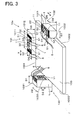
- the electromagnetic coil can be formed with very high efficiency and high accuracy. Also, by forming the electromagnetic coil with the conductive patterns disposed on the outer peripheral surface of the insulator, a very small magneto-impedance sensor element can be realized. Additionally, the conductive patterns constituting the electromagnetic coil can be formed on the outer peripheral surface of the insulator by, e.g., a method using vapor deposition of a metal, a method of etching a vapor-deposited metallic thin film and selectively removing the metallic thin film, or a method of coating conductive ink. At least one of epoxy resin, silicone, etc. can be employed as the insulator.
- This example is related to a three-dimensional magnetic bearing sensor 10a employing a magneto-impedance sensor element 10 with an electromagnetic coil. Details of the three-dimensional magnetic bearing sensor 10a will be described below with reference to Figs. 1 to 14. As shown in Figs. 1 to 3, the three-dimensional magnetic bearing sensor 10a of this example includes a first sensor 101, a second sensor 102, and a third sensor 103 each constituted by the magneto-impedance sensor element 10.
- the magneto-impedance sensor element 10 comprises a magnetic sensitive member 2 having a characteristic changed responsive to an external magnetic field, an insulator 4 formed to allow penetration of the magnetic sensitive member 2 through it, and an electromagnetic coil 3 made up of foil-like conductive patterns 31, 32 arranged in adjacent relation on an outer surface of the insulator 4.
- the first sensor 101, the second sensor 102, and the third sensor 103 are disposed such that directions in which the respective magnetic sensitive members 2 have maximum magnetic field detection sensitivities are substantially orthogonal to each other. Details of those sensors will be described below.
- the magneto-impedance sensor element 10 constituting each of the first sensor 101, the second sensor 102, and the third sensor 103 comprises, as shown in Figs. 1 and 2, an electrode-wiring substrate 1 having an elongate groove 11 formed therein as a recessed groove, first conductive patterns 31 which are disposed on an inner peripheral surface of the elongate groove 11 to extend substantially perpendicularly to the groove-running direction of the elongate groove 11 and each of which has opposite ends extended to position on the surface of the electrode-wiring substrate 1, the insulator 4 filled in the elongate groove 11 in a state that an amorphous wire serving as the magnetic sensitive member 2 (hereinafter referred to also as an "amorphous wire 2") penetrates the insulator 4, and second conductive patterns 32 disposed on an outer surface of the insulator 4 in bridging relation to the elongate groove 11.
- the electromagnetic coil 3 in this example is a combination of one coil portion constituted by each of the first conductive patterns 31 and the other coil portion
- the first sensor 101 is disposed with its amorphous wire 2 extending in the X-direction of an IC 100
- the second sensor 102 is disposed with its amorphous wire 2 extending in the Y-direction of the IC 100
- the third sensor 103 is disposed with its amorphous wire 2 extending in the Z-direction of the IC 100.
- the MI element 10 comprises, as shown in Figs. 1 and 2, the electrode-wiring substrate 1 having the elongate groove 11 formed therein, the amorphous wire 2 having a characteristic changed responsive to a magnetic field acting upon it, the electromagnetic coil 3 wound around the amorphous wire 2 with the insulator 4 interposed between them, and electrodes 52, 51 formed as terminals extended respectively from the amorphous wire 2 and the electromagnetic coil 3.
- the amorphous wire 2 is a magnetic wire having a diameter of 20 ⁇ m and exhibiting electrical conductivity.
- the elongate groove 11 formed in the electrode-wiring substrate 1 has a depth of 50 ⁇ m and a width of 70 ⁇ m, and the amorphous wire 2 is placed in the elongate groove 11 to extend in the groove-running direction.
- the insulator 4 made of epoxy resin is filled in the elongate groove 11 in which the amorphous wire 2 is placed.
- the electromagnetic coil 3 forms a spiral electric path as a whole by, as described above, combining one coil portion constituted by the first conductive pattern 31 disposed on an inner peripheral surface 111 of the elongate groove 11 and the other coil portion constituted by the second conductive pattern 32 which is disposed on the outer surface of the insulator 4 and is extended on the surface of the electrode-wiring substrate 1 in bridging relation to the elongate groove 11.
- the conductive pattern 31 is formed substantially perpendicularly to the groove-running direction of the elongate groove 11.
- the conductive pattern 32 is formed obliquely relative to the width direction of the elongate groove 11 for electrical connection between the respective corresponding ends of the conductive patterns 31 adjacent to each other.
- the conductive pattern 32 may be disposed to extend in the width direction of the elongate groove 11, and the conductive pattern 31 may be formed obliquely relative to the width direction of the elongate groove 11.
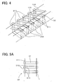
- a method of forming the conductive patterns 31 disposed on the inner peripheral surface 111 of the elongate groove 11 will now be described with reference to Figs. 4 to 6.
- a conductive metallic thin film was first vapor-deposited over the entire inner peripheral surface 111 of the elongate groove 11 formed to extend in the lengthwise direction of the electrode-wiring substrate 1 and on vicinity area of the elongate groove 11 on the surface of the electrode-wiring substrate 1. Then, parts of the metallic thin film were selectively removed by selective etching to form the conductive patterns 31 comprising vertical patterns 311 and horizontal patterns 312.
- the vertical patterns 311 were formed to vertically extend on both groove side surfaces 113 of the elongate groove 11, and the horizontal patterns 312 were formed on a groove bottom surface 110 of the elongate groove 11 to interconnect the corresponding vertical patterns 311 positioned to face each other.
- a conductive metallic thin film was first vapor-deposited on the surface of the electrode-wiring substrate 1, in which the elongate groove 11 was filled with the insulator 4, so as to cover an area of the upper surface 112 of the elongate groove 11 and the vicinity thereof. Then, as shown in Figs. 4 to 6, the metallic thin film was partly removed by selective etching to form the conductive patterns 32 for interconnecting the respective corresponding ends of the conductive patterns 31 adjacent to each other. Additionally, as shown in Fig.
- each vertical pattern 311 and each horizontal pattern 312 in the groove-running direction can be set to, e.g., 50 ⁇ m or 10 ⁇ m, and the width of each gap between the adjacent patterns can be set to, e.g., 25 ⁇ m or 5 ⁇ m, namely half of the pattern width.
- the width of each pattern 311, 312 in the groove-running direction may be set to 25 ⁇ m, and the width of each gap between the adjacent patterns may be set to the same value, i.e., 25 ⁇ m.
- the insulator 4 is interposed between the amorphous wire 2 and the electromagnetic coil 3 to maintain electrical insulation between the amorphous wire 2 and the electromagnetic coil 3.
- the electromagnetic coil 3 is directly formed on an outer periphery of the insulator 4 through which the amorphous wire 2 penetrates.
- the inner diameter of the electromagnetic coil 3 can be reduced to a very small value of not larger than 200 ⁇ m, and therefore a reduction in overall size of the MI element 10 is realized.
- the amorphous wire 2 with a diameter of 1 to 150 ⁇ m, the diameter of the electromagnetic coil 3 can be further reduced.
- the circle-equivalent inner diameter (diameter of a circle having the same cross-sectional area as that of a groove defined by a height and a width) of the electromagnetic coil 3 is set to a very small value, i.e., 66 ⁇ m.
- the elongate groove 11 is formed in an upper surface 1011, an upper surface 1021, or a side wall surface 1032 thereof, respectively, and the electromagnetic coil 3 is formed to extend in the groove-running direction of the elongate groove 11.
- the insulator 4 is filled in a space having a substantially rectangular shape in cross-section and being positioned on the inner peripheral side of the electromagnetic coil 3.
- the amorphous wire serving as the magnetic sensitive member 2 penetrates the insulator 4 in the groove-running direction substantially at the center of its cross-section.
- the electrode-wiring substrate 1 has dimensions of 0.5 mm ⁇ 0.4 mm ⁇ 1.0 mm.
- the amorphous wire 2 is made of a CoFeSiB-based alloy and has a diameter of 20 ⁇ m and a length of 1 mm.
- the elongate groove 11 is formed to extend in the lengthwise direction of the electrode-wiring substrate 1.
- each sensor 101, 102 and 103 has electrodes 5 formed on each upper surface 1011, 1021 and 1031 of the electrode-wiring substrate 1.
- the electrodes 5 are in total four, i.e., a pair of electrodes 51 extended from the electromagnetic coil 3 and a pair of electrodes 52 extended from the amorphous wire 2.
- the electrodes 51 extended from opposite ends of the electromagnetic coil 3 and the electrodes 52 extended from opposite ends of the amorphous wire 2 are disposed on each of the upper surfaces 1011, 1021 of the first sensor 101 and the second sensor 102.
- the electrodes 52 were arranged near opposite ends of each sensor 101, 102, and the electrode 51 were arranged between the pair of electrodes 52.
- the electrodes 51, 52 are constituted to be electrically connectable to electrode pads (not shown) formed on the IC 100 through respective leads 6 (see Fig. 3).
- the electrodes 52 extended from opposite ends of the amorphous wire 2 and the electrodes 51 extended from opposite ends of the electromagnetic coil 3 are all arranged on the upper surface 1031 adjacent to the side wall surface 1032 through a sensor's ridgeline located at one end in the lengthwise direction thereof.
- Those electrodes 51, 52 are extended from the amorphous wire 2 or the electromagnetic coil 3 for electrical connection via respective conductive patterns disposed on the side wall surface 1032.
- the electrodes 51, 52 of the third sensor 103 are constituted to be electrically connectable to electrode pads (not shown) formed on the IC 100 through respective leads 6 (see Fig. 3).
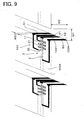
- a method of forming the electrodes 51, 52 on the upper surface 1031 of the third sensor 103 will now be described with reference to Fig. 9.
- a groove 1034 having a predetermined width is formed outside each of opposite lengthwise ends of the electrode-wiring substrate 1 constituting the third sensor 103 (Fig. 9 shows only one end as a typical example).
- the electrodes 51, 52 are formed respectively to extend from the electromagnetic coil 3 or the amorphous wire 2 so as to cover an inner wall surface of the groove 1034, i.e., an end surface of the third sensor 103.
- the third sensor 103 is obtained by cutting out the electrode-wiring substrate 1 at the groove 1034.
- the elongate groove 11 and joint pads are formed on the side surface 1032 by etching or the like.
- the third sensor 103 was fabricated by employing a photolithographic process (semiconductor technique).
- the pads formed on the side surface 1032 of the third sensor 103 are positioned in abutment with a side wall surface 1003 of the IC 100.
- the three-dimensional magnetic bearing sensor 10a of this example is constructed by mounting, to the IC 100, the sensors 101 to 103 each being made of the MI element 10 and substantially in the form of a parallelepiped, as shown in Fig. 3.
- the first sensor 101 is to measure a magnetic field component in the X-direction
- the second sensor 102 is to measure a magnetic field component in the Y-direction
- the third sensor 103 is to measure a magnetic field component in the Z-direction (i.e., the direction of thickness of the IC 100).
- the IC 100 is, as shown in Fig. 3, in the form of a rectangular plate having four side wall surfaces in orthogonal relation to each other.
- the first sensor 101 and the second sensor 102 are mounted respectively to adjacent side wall surfaces 1001, 1002 of the rectangular plate.
- the third sensor 103 is mounted to another one of the side wall surfaces of the IC 100, namely a side wall surface 1003 substantially parallel to the side wall surface 1002 (or a side wall surface substantially parallel to the side wall surface 1001).
- the first sensor 101 has the elongate groove 11 formed in its upper surface 1011 to extend in the lengthwise direction thereof. Then, the first sensor 101 is mounted in a state that the side wall surface 1012 adjacent to the upper surface 1011 with intermediation of the sensor's ridgeline located at one end in the lengthwise direction is abutted with the side wall surface 1001 of the IC 100.
- the second sensor has the elongate groove 11 formed in its lengthwise upper surface 1021 to extend in the lengthwise direction thereof. Then, the second sensor 102 is mounted in a state that the side wall surface 1022 adjacent to the upper surface 1021 with intermediation of the sensor's ridgeline located at one end in the lengthwise direction is abutted with the side wall surface 1002 of the IC 100.
- the third sensor has the elongate groove 11 formed in its lengthwise side wall surface 1032 to extend substantially perpendicularly to the lengthwise direction thereof. Then, the third sensor 103 is mounted in a state that the side wall surface 1032 in which the elongate groove 11 is formed is abutted with the side wall surface 1003 of the IC 100.
- the side wall surface 1001 defines the X-direction
- the side wall surface 1002 defines the Y-direction
- the Z-direction is defined in orthogonal relation to both the X-and Y-directions.
- the first sensor 101 is disposed such that the groove-running direction of its elongate groove 11 is substantially matched with the X-direction.
- the second sensor 102 is disposed such that the groove-running direction of its elongate groove 11 is substantially matched with the Y-direction.
- the third sensor 103 is disposed such that the groove-running direction of its elongate groove 11 is substantially matched with the Z-direction.
- each of the first sensor 101 to the third sensor 103 has dimensions of 0.5 mm x 0.4 mm x 1.0 mm. Therefore, the three-dimensional magnetic bearing sensor 10a of this example, which comprises those small sensors 101 to 103 each constituted by the MI element 10, has very small dimensions of 2.0 mm ⁇ 1.8 mm ⁇ 1.0 mm, and hence has a size capable of realizing superior mountability.
- the first sensor 101 and the second sensor 102 are electrically connected to the IC 100 via the respective leads 6 which are connected to the electrodes 51, 52 formed on their upper surfaces 1011, 1021.
- the third sensor 103 is electrically connected to the IC 100 via the respective leads 6 which are connected to the electrodes 51, 52 formed on its upper surface 1031.
- an external magnetic field acting upon the magnetic sensitive member 2 is detected by measuring a voltage generated in the electromagnetic coil when a high-frequency wave or a pulse current is applied to the amorphous wire 2.
- the three-dimensional magnetic bearing sensor 10a of this example has an integrated electronic circuit shown in Fig. 10. The electronic circuit is designed to make a current change in a high-frequency range act upon the amorphous wire 2 and to measure an induced voltage that is generated in the electromagnetic coil 3 at that time, thereby measuring the intensity of the acting magnetic field.
- the electronic circuit comprises a signal generator 6, the sensors 101 to 103, and a signal processing circuit 7.
- the signal generator 6 generates, at signal intervals of 1 ⁇ sec, a pulse signal including mainly 200 MHz and having the intensity of 170 mA.
- the electronic circuit applies the pulse signal to the amorphous wire 2.
- Each of the sensors 101 to 103 utilizes the phenomenon that a voltage is induced in the electromagnetic coil 3 depending on an external magnetic field acting upon the amorphous wire 2.
- the induced voltage in the electromagnetic coil 3 generates at the time of rise or fall of the pulse signal.
- the signal processing circuit 7 is a circuit designed so as to process the induced voltage of the electromagnetic coil 3.
- the induced voltage of the electromagnetic coil 3 is taken out through synchronous detection 71 that is turned on/off in sync with the pulse signal, and the taken-out induced voltage is amplified by an amplifier 72 at a predetermined amplification factor. Then, the signal amplified by the signal processing circuit 7 is output as an output signal of the electronic circuit.
- a cutoff time required for the pulse signal to fall from 90% to 10% of a steady-state value was set to 4 nano seconds.
- respective magnetic field components in the X-, Y- and -Z directions are detected by using three MI elements 10 (i.e., the first sensor 101, the second sensor 102, and the third sensor 103) disposed in the predetermined positions of the IC 10.
- the sensors 101 to 103 output X-, Y- and Z-axis outputs having respective phases different from each other, as shown in Figs. 11 to 13, to the signal processing circuit 7 (Fig. 10) formed in the IC 100.
- Fig. 11 shows changes in output signals of a horizontal component of terrestrial magnetism, which were detected by the first sensor 101 and the second sensor 102 when rotating the three-dimensional magnetic bearing sensor 10a through 360 degrees about the Z-axis in which the elongate groove 11 of the Z-axis direction sensor, i.e., the third sensor 103, was oriented in the vertical direction.
- Fig. 12 shows changes in output signals detected by the first sensor 101 and the third sensor 103 when rotating the three-dimensional magnetic bearing sensor 10a about the Y-axis in which the elongate groove 11 of the Y-axis direction sensor, i.e., the second sensor 102, was oriented in the vertical direction.
- Fig. 12 shows changes in output signals detected by the first sensor 101 and the third sensor 103 when rotating the three-dimensional magnetic bearing sensor 10a about the Y-axis in which the elongate groove 11 of the Y-axis direction sensor, i.e., the second sensor 102, was oriented in the vertical direction.
- FIG. 13 shows changes in output signals detected by the second sensor 102 and the third sensor 103 when rotating the three-dimensional magnetic bearing sensor 10a about the X-axis in which the elongate groove 11 of the X-axis direction sensor, i.e., the first sensor 101, was oriented in the vertical direction.
- the horizontal axis represents a rotational angle about each axis
- the vertical axis represents a magnitude of the output signal of each sensor 101, 102 and 103.
- the three-dimensional magnetic bearing sensor 10a With the three-dimensional magnetic bearing sensor 10a, simultaneous magnetic sensing in the X-, Y- and Z-directions, which has faced a difficulty in the related art, can be performed by employing three MI elements 10 with high accuracy while realizing a reduction in size. Accordingly, the three-dimensional magnetic bearing sensor 10a can detect an external magnetic field acting upon it with high accuracy regardless of the sensor posture.
- the third sensor 103 is fabricated with a two-dimensional process and is joined to one side surface of the IC 100 by bonding while the third sensor 103 is held upright. Therefore, a three-dimensional process requiring a high cost is no longer required, and a cost reduction can be realized.
- the MI element 10 has a structure utilizing the elongate groove 11 formed in the electrode-wiring substrate 1. Accordingly, the sensor size can be reduced as compared with the case of arranging, for example, a bobbin including an electromagnetic coil wound around it on the electrode-wiring substrate 1. It is also possible to prevent the electromagnetic coil 3 from being externally touched, and to improve mechanical stability.
- the amorphous wire 2 is used as the magnetic sensitive member.
- the output voltage per winding of the electromagnetic coil 3 can be further increased, and hence the number of windings can be further reduced. This means that the axial length of the MI element 10 can be further shortened.
- the winding pitch of the electromagnetic coil 3 is realized at 50 ⁇ m, i.e., a value not larger than 100 ⁇ m.
- the output voltage can be increased.
- that effect of increasing the output voltage can be obtained by setting the winding pitch per unit length of the electromagnetic coil 3 to be not larger than 100 ⁇ m as in this example. Then, the length of the MI element 10 can be relatively reduced with respect to the output voltage.
- the first sensor 101 and the second sensor 102 are disposed respectively on the adjacent side wall surfaces 1001, 1002 of the IC 100 that is substantially in the rectangular form and has four side wall surfaces.
- the third sensor 103 is disposed on one 1003 of the remaining two side wall surfaces.
- the sensors 101 to 103 are arranged in an efficient way.
- sensors having the same specifications are employed as the first sensor 101 and the second sensor 102, the number of types of parts constituting the three-dimensional magnetic bearing sensor 10a can be restrained and hence a cost reduction is realized.
- this example employs the third sensor 103 differing in shape and dimensions from the first and second sensors 101, 102, the first to third sensors 101 to 103 may be all designed to have the same shape and dimensions instead.
- the third sensor 103 may be disposed on the side wall surface 1001 instead, on which the first sensor 101 is disposed, as shown in Fig. 14 ((A) of Fig. 14). Also, the third sensor 103 may be disposed on the side wall surface 1002 on which the second sensor 102 is disposed (Fig. 14(B)). Alternatively, the first to third sensors 101 to 103 may be disposed on the same side wall surface (Fig. 14(C)), or the first to third sensors 101 to 103 may be disposed on an upper (or lower) surface of the IC 100 (Fig. 14(D)).
- a known sensor shown in Fig. 16 i.e., a bobbin element 9 constituted by a known bobbin-type MI element, was employed as a comparative example.
- the bobbin element 9 comprises an amorphous wire 92 and an electromagnetic coil 93 with an insulating winding frame (bobbin) 94 interposed between them, to thereby maintain electrical insulation.
- the amorphous wire 92 used here as the magnetic sensitive member is made of a CoFeSiB-based alloy and has a diameter of 30 ⁇ m.
- the electromagnetic coil 93 has an inner diameter of 1.5 mm.
- the winding frame 94 is provided with two electrodes 95 extended from electromagnetic coil 93 and other two electrodes 95 extended from the amorphous wire 92.
- the bobbin element 9 has dimensions of 3 mm ⁇ 2 mm ⁇ 4 mm.
- the known bobbin element 9 has a large bulk.
- Fig. 15 shows results of comparing a magnetic detection characteristic between the known sensor constituted by the known bobbin element 9 (wire length; 2.5 mm, coil diameter; 1.5 mm, and 40 turns) and the novel structure sensor (wire diameter; 20 ⁇ m, wire length; 1.0 mm, coil diameter (circle-equivalent diameter); 66 ⁇ m, and 18 turns).
- the horizontal axis represents an external magnetic field
- the vertical axis represents an output voltage from the signal processing circuit.
- the known sensor and the novel structure sensor of this example have linear ranges substantially equal to each other, i.e., about ⁇ 3 G, and the output voltage of the novel structure sensor of this example is 80% or more of that of the known sensor.
- a lowering of the output voltage is restrained for a reduction in size and thickness.
- the MI element constituting the novel structure sensor of this example is superior in voltage per turn to the bobbin element 9. Comparing with 28 mV/turn of the bobbin element 9, the MI element constituting the novel structure sensor of this example produces about twice voltage per turn, i.e., 53 mV/turn.
- the novel structure sensor of this example has a superior characteristic, as shown in Fig. 15, that a good linearity is obtained in the magnetic field range of ⁇ 3G.
- the other construction and operating advantages are the same as those in Example 1.
- each of the sensors 101 to 103 constituting the three-dimensional magnetic bearing sensor of Example 1 was evaluated for a characteristic in detection of terrestrial magnetism. Details of the evaluation will be described below with reference to Figs. 3, 7 to 9, and Tables 1 to 4.
- D5 in Figs. 3 and 7 denotes the width of the first sensor 101
- D4 denotes the length of the first sensor 101 in the lengthwise direction
- D6 denotes the height of the first sensor 101.
- D7 in Figs. 3 and 7 denotes the width of the second sensor 102
- D8 denotes the length of the second sensor 102 in the lengthwise direction
- D9 denotes the height of the second sensor 102.
- D1 in Figs. 3 and 8 denotes the width of the third sensor 103
- D2 denotes the length of the third sensor 103 in the lengthwise direction
- D3 denotes the height of the third sensor 103.
- Table 1 lists, for the various dimensions D1 to D9 shown in Fig. 3, design values, values actually measured in the sensors, and allowable values (dimension allowable ranges) in units of mm.
- Table 1 design values values actually measured allowable values unit D1 0.6 0.4 ⁇ 0.9 0.2 ⁇ 1.2 mm D2 1.2 0.5 ⁇ 1.5 0.3 ⁇ 2.0 mm D3 1.0 0.8 ⁇ 1.2 0.3 ⁇ 2.5 mm D4 1.0 0.6 ⁇ 1.6 0.2 ⁇ 2.5 mm D5 0.5 0.2 ⁇ 1.0 0.2 ⁇ 2.0 mm D6 0.4 0.2 ⁇ 0.6 0.2 ⁇ 2.5 mm D7 0.5 0.3 ⁇ 1.1 0.2 ⁇ 2.0 mm D8 1.0 0.8 ⁇ 1.5 0.2 ⁇ 2.5 mm D9 0.4 0.2 ⁇ 0.8 0.2 ⁇ 2.5 mm
- W34 in Fig. 8 denotes the width of each of the conductive patterns 31 formed on the inner peripheral surface 111 of the elongate groove 11 which is formed in the third sensor 103
- W35 denotes the pitch of the conductive patterns 31 adjacent to each other.
- Table 2 lists, for the various dimensions D1 to D3, W34 and W35 shown in Fig. 8, design values, values actually measured in the sensors, and allowable values (dimension allowable ranges) in units of mm.
- Table 2 design values values actually measured allowable values unit D1 0.6 0.2 ⁇ 0.8 0.2 ⁇ 1.2 mm D2 1.2 0.6 ⁇ 1.6 0.3 ⁇ 2.0 mm D3 1.0 0.5 ⁇ 1.4 0.3 ⁇ 2.5 mm W34 0.025 0.010 ⁇ 0.050 0.005 ⁇ 0.100 mm W35 0.025 0.015 ⁇ 0.040 0.005 ⁇ 0.100 mm
- D6 (D9) in Fig. 7 denotes the height of the first sensor 101 (second sensor 102)
- D5 (D7) denotes the width of the first sensor 101 (second sensor 102)
- D4 (D8) denotes the length of the first sensor 101 (second sensor 102) in the lengthwise direction.
- W14 (W24) in Fig. 7 denotes the width of each of the conductive patterns 31 formed on the inner peripheral surface 111 of the elongate groove 11 which is formed in the first sensor 101 (second sensor 102) to extend in the lengthwise direction of the electrode-wiring substrate 1, and W15 (W25) denotes the array pitch of the conductive patterns 31 adjacent to each other.
- Table 3 lists, for the various dimensions D4 to D6, W14 and W15 (D7 to D9, W24 and W25) shown in Fig. 7, design values, values actually measured in the sensors, and allowable values (dimension allowable ranges) in units of mm.
- M1 in Fig. 9 denotes the width of the groove 1034 formed in the process of manufacturing the third sensor 103
- M2 denotes the depth of the groove 1034
- W53 denotes the width of each of the electrodes 51, 52 formed to extend on the wall surface of the groove 1034.
- the third sensor 103 is obtained by dividing the substrate at the groove 1034 in a later step.
- Table 4 lists, for the various dimensions M1, M2 and W53 shown in Fig. 9, design values, values actually measured in the sensors, and allowable values (dimension allowable ranges) in units of mm.
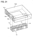
- This example represents a modification in which the construction of the MI element 10 is modified on the basis of Example 1. Details of this modification will be described below with reference to Figs. 17 to 21.
- the electromagnetic coil 3 is formed on an outer peripheral surface of the insulator 4 disposed around the amorphous wire 2.
- the electromagnetic coil 3 is formed by conductive patterns 33 disposed on the outer peripheral surface of the insulator 4.
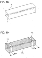
- the insulator 4 made of resin was formed by molding around the amorphous wire 2.
- the insulator 4 is in the form of a rod having a rectangular cross-section, and opposite ends of the amorphous wire 2 are exposed at opposite end surfaces of the insulator 4.
- the electromagnetic coil 3 was formed through the following steps. First, a metal material containing copper was vapor-deposited all over the outer peripheral surface of the rod-shaped insulator 4, thereby forming a metallic thin film. Then, the metallic thin film was partly removed by selective etching to form the electromagnetic coil 3. At the same time as forming the electromagnetic coil 3, in this example, electrodes 52 extended from the opposite ends of the amorphous wire 2 and electrodes 51 extended from opposite ends of the electromagnetic coil 3 were also formed.
- the metallic thin film was removed in ring-shaped areas at positions away from opposite ends of the insulator 4 by a predetermined distance WD1, thus dividing the metallic thin film into three parts. Thereafter, selective-etching was performed on an intermediate metallic thin film 30a to form the conductive patterns 33 constituting the electromagnetic coil 3 and the electrodes 51 extended from the opposite ends of the electromagnetic coil 3.
- Metallic thin films 30b at the opposite ends of the electromagnetic coil 3 are electrically connected to the corresponding ends of the amorphous wire 2 penetrating the insulator 4 and function as the electrodes 52 for the amorphous wire 2.
- a three-dimensional magnetic bearing sensor 10a of this example is constructed, as shown in Fig. 20, by employing three MI elements 10 directly or indirectly disposed on the IC 100.
- Two MI elements 10 are disposed on the surface of the IC 100 to serve respectively as a first sensor 101 and a second sensor 102 for measuring the intensities of a magnetic field in the X- and Y-directions, i.e., two orthogonal directions in the surface of the IC 100.
- a third sensor 103 for measuring the intensity of a magnetic field in the Z-direction, i.e., the direction of thickness of the IC 100 is constituted by surface-mounting the MI element 10 to a daughter substrate 100d.
- the third sensor 103 is joined to one side wall surface of the IC 100 by employing pads formed on a rear surface of the daughter substrate 100d.
- the daughter substrate 100d has electrodes formed corresponding to the electrodes 51, 52 of the MI element. Further, electrodes 51d, 52d extended respectively from those electrodes on the daughter substrate 100d are disposed on one side wall surface thereof.
- the electrodes 51d, 52d are constituted to be electrically connectable to corresponding electrodes (not shown) of the IC 100 via similar leads to those used in Example 1.
- Example 1 a member in the form of a thin film, i.e., a magnetic anisotropic thin film, can also be used.
- the magnetic anisotropic thin film is covered with the insulator 4 to have a substantially rectangular cross-section. Then, the electromagnetic coil 33 and the electrodes 51, 52 are formed through the same steps as those described above.
- a three-dimensional magnetic bearing sensor 10a of this example has a common substrate 109 on which the IC 100 and the sensors 101 to 103 are all disposed.
- the three-dimensional magnetic bearing sensor 10a shown in Fig. 22 is constructed on the basis of Example 1 by mounting the IC 100 on a mount surface of the common substrate 109, and by arranging the first sensor 101, the second sensor 102, and the third sensor 103 onto side wall surfaces of the common substrate 109.
- the three-dimensional magnetic bearing sensor 10a shown in Fig. 23 is constructed on the basis of the three-dimensional magnetic bearing sensor of Example 4 by mounting the IC 100 on the mount surface of the common substrate 109, and by arranging the first sensor 101, the second sensor 102, and the third sensor 103 onto the side wall surfaces of the common substrate 109.
- the other construction and operating advantages are the same as those in Example 1 or 4.
Landscapes
- Physics & Mathematics (AREA)
- General Physics & Mathematics (AREA)
- Condensed Matter Physics & Semiconductors (AREA)
- Engineering & Computer Science (AREA)
- Remote Sensing (AREA)
- Radar, Positioning & Navigation (AREA)
- Life Sciences & Earth Sciences (AREA)
- Environmental & Geological Engineering (AREA)
- General Life Sciences & Earth Sciences (AREA)
- Geology (AREA)
- Electromagnetism (AREA)
- Nanotechnology (AREA)
- Chemical & Material Sciences (AREA)
- Measuring Magnetic Variables (AREA)
- Hall/Mr Elements (AREA)
Abstract
A three-dimensional magnetic bearing sensor 10a includes a first sensor 101, a second sensor 102, and a third sensor 103 each constituted by a magneto-impedance sensor element 10 comprising a magnetic sensitive member 2 having a characteristic changed responsive to an external magnetic field, an insulator 4 formed to allow penetration of the magnetic sensitive member 2 therethrough, and an electromagnetic coil 3 made up of foil-like conductive patterns 31, 32 arranged in adjacent relation on an outer surface of the insulator 4. The first sensor 101, the second sensor 102, and the third sensor 103 are disposed such that directions in which the magnetic sensitive members 2 in respective sensors have maximum magnetic field detection sensitivities are substantially orthogonal to each other.
Description
- The present invention relates to a three-dimensional magnetic bearing sensor and a magneto-impedance sensor element, which can be applied to an electronic compass.
- Hitherto, there is known a magnetic sensor wherein a one-piece element holding an amorphous wire as a magnetic sensitive member therein is inserted in a tubular bobbin around which a detection coil and a negative feedback coil are wound (see, e.g., Patent Document 1). The one-piece element is manufactured, for example, by arranging the amorphous wire between electrodes disposed at opposite ends of a substrate in its lengthwise direction, and by covering the entire substrate with a gel-like material.
Further, a magnetic bearing sensor comprising two or three sets of thus-constructed magnetic sensors is also known. In that magnetic bearing sensor, individual magnetic sensors are arranged such that the axial directions of respective amorphous wires are substantially orthogonal to each other (see, e.g., Patent Document 2). -
- Patent Document 1: Japanese Unexamined Patent Application Publication No. 2001-296127
- Patent Document 2: Japanese Unexamined Patent Application Publication No. 11-64473
- However, the known magnetic sensor has the following problems. The magnetic sensor has the structure that the one-piece element having the amorphous wire arranged on the substrate is employed and it is inserted in the tubular bobbin for placement therein. Accordingly, the number of parts and the number of manufacturing steps are increased, and the manufacturing and assembly steps are complicated. Thus, the known magnetic sensor is not adapted for a reduction in size and cost of the sensor.
- Also, the known magnetic bearing sensor comprising three sets of magnetic sensors each constructed as described above has the following problems. In addition to an insufficient reduction in size and cost as in the known magnetic sensor, the magnetic bearing sensor comprising three sets of magnetic sensors necessarily accompanies a risk of further enlarging the bulk and increasing the cost. Means for Solving the Problems
- A first aspect of the present invention resides in a three-dimensional magnetic bearing sensor including a first sensor, a second sensor, and a third sensor each constituted by a magneto-impedance sensor element comprising a magnetic sensitive member having a characteristic changed responsive to an external magnetic field, an insulator formed to allow penetration of the magnetic sensitive member therethrough, and an electromagnetic coil made up of foil-like conductive patterns arranged in adjacent relation on an outer surface of the insulator,
wherein the first sensor, the second sensor, and the third sensor are disposed such that directions in which the magnetic sensitive members in respective sensors have maximum magnetic field detection sensitivities are substantially orthogonal to each other. - The three-dimensional magnetic bearing sensor according to the first aspect of the present invention is constituted by employing the first sensor, the second sensor, and the third sensor each constituted by the magneto-impedance sensor element comprising the magnetic sensitive member having a characteristic changed responsive to an external magnetic field, the insulator formed to allow penetration of the magnetic sensitive member therethrough, and the electromagnetic coil made up of the foil-like conductive patterns arranged in adjacent relation on the outer surface of the insulator. Further, in this three-dimensional magnetic bearing sensor, those sensors are disposed such that the directions in which the magnetic sensitive members in respective sensors have maximum magnetic sensitivities are substantially orthogonal to each other.
- Here, the electromagnetic coil in each sensor is made up of the foil-like conductive patterns. The electromagnetic coil made up of the foil-like conductive patterns can be formed in small size with very high efficiency, for example, by a method using vapor deposition of a metal, a method of etching a metallic thin film and selectively removing the metallic thin film, or a method of coating conductive ink. Therefore, each sensor can be formed in small size and at a low cost. Further, with the electromagnetic coil formed of the conductive patterns, the accuracy in forming the electromagnetic coil is increased, whereby variations in characteristics can be reduced and a highly accurate sensor can be realized.
- Moreover, in the three-dimensional magnetic bearing sensor, the first to third sensors are disposed such that the directions in which the magnetic sensitive members in respective sensors have maximum magnetic sensitivities are substantially orthogonal to each other. Accordingly, the three-dimensional magnetic bearing sensor employing those sensors each having high quality can be obtained as a superior product having a small size, a low cost and high accuracy.
- Thus, the three-dimensional magnetic bearing sensor according to the first aspect of the present invention has succeeded in realizing not only easier manufacturing and assembly, but also a smaller size. Also, the three-dimensional magnetic bearing sensor enables highly accurate bearing detection to be performed regardless of its posture.
- A second aspect of the present invention resides in a magneto-impedance sensor element made by winding an electromagnetic coil around a magnetic sensitive member having a characteristic changed responsive to an external magnetic field,
wherein the magneto-impedance sensor element comprises a sensor substrate for holding the magnetic sensitive member, an insulator formed to allow penetration of the magnetic sensitive member therethrough, and an electromagnetic coil made up of foil-like conductive patterns arranged in adjacent relation on an outer surface of the insulator, and
wherein the sensor substrate has electrodes extended from the electromagnetic coil and the magnetic sensitive member, the electrodes being formed on one of outer surfaces of the sensor substrate which is substantially orthogonal to the axial direction of the magnetic sensitive member. - The substrate in the magneto-impedance sensor element according to the second aspect of the present invention has the electrodes extended from the electromagnetic coil and the magnetic sensitive member, and the electrodes are formed on one of outer surfaces of the substrate which is substantially orthogonal to the axial direction of the magnetic sensitive member. Therefore, the magneto-impedance sensor element is suitable for the case in which, when mounting the magneto-impedance sensor element to an electronic circuit board or the like, the axial direction of the magnetic sensitive member is to be set in the direction of thickness of the electronic circuit board or the like. In other words, because the surface of the magneto-impedance sensor element on which the electrodes are disposed can be positioned to face in the same direction as that of a mount surface of the electronic circuit board or the like, it is possible to easily perform connection work using leads, etc.
Further, the magneto-impedance sensor element can be fabricated with a two-dimensional process. Therefore, a three-dimensional process requiring a high cost is no longer required, and a cost reduction can be realized. - The magneto-impedance sensor element includes the electromagnetic coil made up of the foil-like conductive patterns arranged in adjacent relation on the outer surface of the insulator which is formed to allow penetration of the magnetic sensitive member therethrough. The conductive patterns forming the electromagnetic coil can be formed in small size with very high efficiency, for example, by a method using vapor deposition of a metal, a method of etching a metallic thin film and selectively removing the metallic thin film, or a method of coating conductive ink. Therefore, the magneto-impedance sensor element can be formed in small size and at a low cost with high accuracy.
- Thus, the magneto-impedance sensor element according to the second aspect of the present invention can be obtained as a small-sized, highly-accurate, and low-cost element. Further, the magneto-impedance sensor element is suitable for magnetic sensing in the direction of thickness of the electronic circuit board or the like on which the magneto-impedance sensor element is mounted.
-
- [Fig. 1] is a conceptual view showing a front surface of an MI element in Example 1.
- [Fig. 2] is a conceptual view showing a section taken along line A-A in Fig. 1 in which the MI element in Example 1 is shown.
- [Fig. 3] is a perspective view showing an overall construction of a three-dimensional magnetic bearing sensor in Example 1.
- [Fig. 4] is a partial perspective view showing an arrangement of an electromagnetic coil in an elongate groove in Example 1.
- [Fig. 5A] is a partial plan view showing an arrangement of first conductive patterns in an elongate groove in Example 1.
- [Fig. 5B] is a partial plan view showing an arrangement of second conductive patterns in an elongate groove in Example 1.
- [Fig. 6] is a partial plan view showing the arrangement of the electromagnetic coil in the elongate groove in Example 1.
- [Fig. 7] is a perspective view showing first and second sensors in Example 1.
- [Fig. 8] is a perspective view showing a third sensor in Example 1.
- [Fig. 9] is a partial perspective view for explaining an electrode formation of the third sensor in Example 1.
- [Fig. 10] is a block circuit diagram showing an electronic circuit for a three-dimensional magnetic bearing sensor in Example 1.
- [Fig. 11] is a graph showing X- and Y-axis outputs detected by the three-dimensional magnetic bearing sensor in Example 1.
- [Fig. 12] is a graph showing X- and Z-axis outputs detected by the three-dimensional magnetic bearing sensor in Example 1.
- [Fig. 13] is a graph showing Y- and Z-axis outputs detected by the three-dimensional magnetic bearing sensor in Example 1.
- [Fig. 14A] is a plan view showing a construction of another three-dimensional magnetic bearing sensor in Example 1.
- [Fig. 14B] is a plan view showing a construction of still another three-dimensional magnetic bearing sensor in Example 1.
- [Fig. 14C] is a plan view showing a construction of still another three-dimensional magnetic bearing sensor in Example 1.
- [Fig. 14D] is a plan view showing a construction of still another three-dimensional magnetic bearing sensor in Example 1.
- [Fig. 15] is a graph showing the relationship between an external magnetic field acting upon a magnetic sensor employing an MI element and an output voltage in Example 2.
- [Fig. 16] is a front view showing a bobbin-type MI element used for comparison in Example 2.
- [Fig. 17] is a perspective view showing the insulator in Example 4 in which a metallic thin film is removed in a ring-shaped area near each of opposite ends of the insulator.
- [Fig. 18] is a perspective view showing an MI element in Example 4.
- [Fig. 19] is a perspective view showing an insulator molding around the amorphous wire in Example 4.[Fig. 20] is a perspective view showing a three-dimensional magnetic bearing sensor in Example 4.
- [Fig. 21] is a combination view for explaining an MI element and a daughter substrate in Example 4.
- [Fig. 22] is a perspective view showing an overall construction of a three-dimensional magnetic bearing sensor No. 1 in Example 5.
- [Fig. 23] is a perspective view showing an overall construction of a three-dimensional magnetic bearing sensor No. 2 in Example 5.
-
- 1 electrode-wiring substrate
- 11 elongate groove
- 100 IC
- 101 first sensor
- 102 second sensor
- 103 third sensor
- 2 magnetic sensitive member (amorphous wire)
- 3 electromagnetic coil
- 31 first conductive pattern
- 32 second conductive pattern
- 4 insulator
- The magnetic sensitive member in each of the three-dimensional magnetic bearing sensor and the magneto-impedance sensor element according to the first and second aspects of the present invention can be made of, for example, an amorphous wire with a diameter of not larger than 50 µm. In this case, the electromagnetic coil can be formed in a smaller cross-sectional area and the size of the magneto-impedance sensor element can be reduced. More preferably, an amorphous wire with a diameter of not larger than 30 µm is employed. Further, FeCoSiB, NiFe, etc. can be used as materials of the magnetic sensitive member.
- The magneto-impedance sensor element performs magnetic sensing based on the so-called MI phenomenon that an induced voltage generates in the electromagnetic coil responsive to changes of a current supplied to the magnetic sensitive member. The MI phenomenon occurs in the magnetic sensitive member made of a magnetic material having an electron spin direction in the circumferential direction with respect to the direction of the supplied current. When the current supplied to the magnetic sensitive member is abruptly changed, a magnetic field in the circumferential direction is also abruptly changed, and under the action of the changing magnetic field, the directions of electron spin direction are changed depending on the ambient magnetic field. At the same time, there occur changes in, e.g., internal magnetization and impedance of the magnetic sensitive member.- This is the above-mentioned MI phenomenon.
- The magneto-impedance sensor element is a element employing the magnetic sensitive member made of a magnetic material having an electron spin direction in the circumferential direction with respect to the direction of the supplied current. When the current supplied to the magnetic sensitive member is abruptly changed, a magnetic field in the circumferential direction is also abruptly changed, and under the action of the changing magnetic field, the directions of electron spin direction are changed depending on the ambient magnetic field. Then, changes occurred in, e.g., internal magnetization and impedance of the magnetic sensitive member at that time are converted to, for example, a voltage or current generated in the magnetic sensitive member or a voltage or current generated at opposite ends of the electromagnetic coil disposed around the magnetic sensitive member.
- Also, the magneto-impedance sensor element is preferably constructed such that the intensity of an acting magnetic field is determined by measuring the magnitude of an induced voltage generating at the opposite ends of the electromagnetic coil when the current supplied to the magnetic sensitive member is caused to rise or fall in 10 nano seconds or below.
In such a case, with an abrupt change of the supplied current, it is possible to change the magnetic field in the circumferential direction at a speed comparable to the propagation speed of change in electron spin direction in the magnetic sensitive member, and hence to more reliably develop the MI phenomenon. - With a rise or fall of the supplied current in 10 nano seconds or below, a current change including a high-frequency component of about 0.1 GHz can be caused to act upon the magnetic sensitive member. Then, by measuring the induced voltage generating at the opposite ends of the electromagnetic coil, a resulting change of the internal magnetic field generated in the magnetic sensitive member depending on the ambient magnetic field can be measured as the magnitude of the induced voltage, and the intensity of the ambient magnetic field can be measured with higher accuracy. Here, the term "rise or fall of the supplied current" means that a value of the current supplied to the magnetic sensitive member is changed from 10% or below (or 90% or above) of the steady current value to 90% or above (or 10% or below) thereof.
- Preferably, the magneto-impedance sensor element is constructed so as to measure the induced voltage generating at the opposite ends of the electromagnetic coil when the current supplied to the magnetic sensitive member is caused to fall.
The case of abruptly falling the supplied current can provide higher linearity of a signal measured by the magneto-impedance sensor element with respect to the intensity of the magnetic field than the case of raising the supplied current. - In the three-dimensional magnetic bearing sensor according to the first aspect of the present invention, each of the first sensor, the second sensor, and the third sensor may comprise an electrode-wiring substrate having an elongate groove formed therein as a recessed groove, first conductive patterns which are disposed on an inner peripheral surface of the elongate groove to extend across the groove-running direction of the elongate groove and each of which has opposite ends extended to position on the surface of the electrode-wiring substrate, the insulator filled in the elongate groove in a state that an amorphous wire serving as the magnetic sensitive member penetrates the insulator, and second conductive patterns disposed on an outer surface of the insulator in bridging relation to the elongate groove, and
the electromagnetic coil may be a combination of one coil portion constituted by each of the first conductive patterns and the other coil portion constituted by each of the second conductive patterns and electrically connecting respective corresponding ends of the first conductive patterns adjacent to each other. - In that case, with a combination of one coil portion constituted by each of the first conductive patterns disposed on the inner peripheral surface of the elongate groove and the other coil portion constituted by each of the second conductive patterns disposed on the outer surface of the insulator, the electromagnetic coil can be formed in very small size. Therefore, each of the first to third sensors has a small size and the three-dimensional magnetic bearing sensor using those sensors can be obtained as a small-sized one with superior mountability.
- The conductive patterns on the inner peripheral surface of the elongate groove and the outer surface of the insulator can be formed by metal vapor deposition or etching, for example, with very high efficiency and good accuracy. Hence, the three-dimensional magnetic bearing sensor can be manufactured with excellent production efficiency, high accuracy, and good quality.
- The three-dimensional magnetic bearing sensor may include an IC having a substantially rectangular shape with four side wall surfaces and incorporating an electronic circuit formed therein, the first sensor, the second sensor, and the third sensor being all disposed on the IC, and
the third sensor may be disposed on one of the side wall surfaces such that the groove-running direction of the elongate groove is substantially matched with the direction of thickness of the IC. - When the third sensor is disposed on one of the side wall surfaces such that the groove-running direction of the elongate groove is substantially matched with the direction of thickness of the IC, it is possible to efficiently arrange the third sensor for measuring a magnetic field component in the direction of thickness of the IC. On the other hand, the first and second sensors can be mounted onto the surface of the IC, one or more of the side wall surfaces, etc. Because the first and second sensors have their elongate grooves which are required to extend along the surface of the IC, a degree of flexibility in arranging the first and second sensors on the IC is' increased in comparison with that in arranging the third sensor.
- Preferably, the first sensor and the second sensor are disposed on two of the side wall surfaces of the IC which are orthogonal to each other, and the groove-running direction of the elongate groove of each of the first sensor and the second sensor is substantially orthogonal to the side wall surface on which the other sensor is disposed.
When the first sensor and the second sensor are disposed on the two orthogonal side wall surfaces such that the groove-running direction of the elongate groove of each of the first sensor and the second sensor is substantially orthogonal to the side wall surface on which the other sensor is disposed, magnetic field components in the two orthogonal directions in a plane substantially parallel to the IC can be detected. Further, by using a sensor having the same specifications as, e.g., each of the first and second sensors, the number of types of parts can be reduced. - Preferably, the third sensor has electrodes formed on a surface thereof which is positioned to face the same side as that of the surface of the IC, and the electrodes are electrically connected to electrodes disposed on the surface of the IC via leads.
In that case, since the surface of the third sensor on which the electrodes are disposed is oriented substantially in the same direction as the surface of the IC on which the electrodes are disposed, work for connecting the leads can be facilitated. - Preferably, the third sensor has electrodes formed on a surface thereof which is positioned to face the same side as that of the surface of the IC, and the electrodes are electrically connected to electrodes disposed on the surface of the IC via leads, and
each of the first sensor and the second sensor has electrodes formed on a surface thereof which is positioned to face the same side as that of the surface of the IC, and the electrodes are electrically connected to electrodes disposed on the surface of the IC via leads. - In that case, since the surface of each of the first to third sensors on which the electrodes are disposed is oriented substantially in the same direction as the surface of the IC on which the electrodes are disposed, work for connecting the leads can be facilitated.
- The three-dimensional magnetic bearing sensor may have dimensions within 3 mm in length, 3 mm in width and 1.5 mm in height.
When the three-dimensional magnetic bearing sensor is constructed in such a small size, the three-dimensional magnetic bearing sensor is more easily adaptable for portable terminal equipment, e.g., a cellular phone and a PDA. Further, when the three-dimensional magnetic bearing sensor has dimensions within 2.5 mm in length, 2.5 mm in width and 1 mm in height, it can be more easily mounted to the portable terminal equipment. - Preferably, the three-dimensional magnetic bearing sensor includes an IC incorporating an electronic circuit formed therein and a common substrate on which the IC is mounted, the first sensor, the second sensor, and the third sensor being all disposed on the common substrate, and
the third sensor is disposed such that the groove-running direction of the elongate groove is substantially matched with the direction of thickness of the common substrate.
In that case, the first to third sensors can be efficiently arranged together with the IC by employing the common substrate. - Preferably, in each of the first sensor, the second sensor, and the third sensor, the insulator is formed on an outer periphery of an amorphous wire or a magnetic anisotropic thin film serving as the magnetic sensitive member, and the electromagnetic coil is constituted by the conductive patterns arranged on the outer peripheral surface of the insulator.
In that case, since the conductive patterns are formed on the outer peripheral surface of the insulator which receives the magnetic sensitive member penetrating it, the electromagnetic coil can be formed with very high efficiency and high accuracy. Also, by using the electromagnetic coil made up of the conductive patterns formed on the outer peripheral surface of the insulator, each sensor can be formed in very small size. Further, by constituting the three-dimensional magnetic bearing sensor with the use of the first to third sensors each constructed as mentioned above, a small-sized and highly-accurate excellent product can be realized at a low cost with good production efficiency. - Preferably, the three-dimensional magnetic bearing sensor includes an IC having a substantially rectangular shape with four side wall surfaces and incorporating an electronic circuit formed therein, the first sensor, the second sensor, and the third sensor being all disposed on the IC, and
the third sensor is surface-mounted to a daughter substrate which is disposed on one of the side wall surfaces in substantially orthogonal relation to the surface of the IC, and a direction in which the magnetic sensitive member in the third sensor has a maximum magnetic field detection sensitivity is substantially matched with the direction of thickness of the IC.
When the third sensor is disposed such that the direction of magnetic field detection sensitivity is substantially matched with the direction of thickness of the IC, a magnetic field component in the direction of thickness of the IC can be measured by the third sensor. Generally, in each of the first to third sensors, the magnetic field detection sensitivity is maximized in the lengthwise direction of the magnetic sensitive member. Further, the daughter substrate may be vertically disposed on the surface of the IC. - The first sensor and the second sensor may be disposed on the surface of the IC.
By disposing the first sensor and the second sensor on the surface of the IC, a further size reduction can be realized in overall bulk of the three-dimensional magnetic bearing sensor. - The third sensor may have electrodes positioned to face a mount surface of the daughter substrate and may be surface-mounted to the daughter substrate in a state that the electrodes are abutted with corresponding electrodes on the daughter substrate.
In that case, electrical connection between the daughter substrate and the third sensor can be realized with higher reliability. - The third sensor may have electrodes positioned to face a mount surface of the daughter substrate and is surface-mounted to the daughter substrate in a state that the electrodes are abutted with corresponding electrodes on the daughter substrate, and
each of the first sensor and the second sensor may have electrodes positioned to face the surface of the IC and be disposed in a state that the electrodes are abutted with corresponding electrodes on the IC.
In that case, the first to third sensors can be efficiently arranged with respect to the IC, and a small-sized three-dimensional magnetic bearing sensor can be realized. - The three-dimensional magnetic bearing sensor may have dimensions within 3 mm in length, 3 mm in width and 1.5 mm in height.
When the three-dimensional magnetic bearing sensor is constructed in such a small size, the three-dimensional magnetic bearing sensor is more easily adaptable for portable terminal equipment, e.g., a cellular phone and a PDA. Further, when the three-dimensional magnetic bearing sensor has dimensions within 2.5 mm in length, 2.5 mm in width and 1 mm in height, it can be more easily mounted to the portable terminal equipment. - Preferably, the three-dimensional magnetic bearing sensor includes an IC incorporating an electronic circuit formed therein and a common substrate on which the IC is mounted, the first sensor, the second sensor, and the third sensor being all disposed on the common substrate, and
the third sensor is disposed such that a direction in which the magnetic sensitive member in the third sensor has a maximum magnetic field detection sensitivity is substantially matched with the direction of thickness of the common substrate.
In that case, the first to third sensors can be efficiently arranged together with the IC by employing the common substrate. - According to the second aspect of the present invention, the magneto-impedance sensor element may comprise an electrode-wiring substrate serving as the sensor substrate and having an elongate groove formed therein as a recessed groove, first conductive patterns which are disposed on an inner peripheral surface of the elongate groove to extend substantially perpendicularly to the groove-running direction of the elongate groove and each of which has opposite ends extended to position on the surface of the electrode-wiring substrate, the insulator filled in the elongate groove in a state that an amorphous wire serving as the magnetic sensitive member penetrates the insulator, and second conductive patterns disposed on an outer surface of the insulator in bridging relation to the elongate groove, and
the electromagnetic coil may be a combination of one coil portion constituted by each of the first conductive patterns and the other coil portion constituted by each of the second conductive patterns and electrically connecting respective corresponding ends of the first conductive patterns adjacent to each other. - In that case, with a combination of one coil portion constituted by each of the first conductive patterns disposed on the inner peripheral surface of the elongate groove and the other coil portion constituted by each of the second conductive patterns disposed on the outer surface of the insulator, the electromagnetic coil can be formed in very small size. Therefore, the magneto-impedance sensor element can be obtained as a small-sized element with superior mountability. Further, the conductive patterns on the inner peripheral surface of the elongate groove and the outer surface of the insulator can be formed by metal vapor deposition or etching, for example, with very high efficiency and good accuracy. Hence, the magneto-impedance sensor element can be manufactured with excellent production efficiency, high accuracy, and good quality.
- The magneto-impedance sensor element may comprise an insulator covering an outer periphery of an amorphous wire or a magnetic anisotropic thin film serving as the magnetic sensitive member, the electromagnetic coil constituted by the conductive patterns arranged on the outer peripheral surface of the insulator, and a daughter substrate serving as the sensor substrate on which the insulator receiving the magnetic sensitive member therein is disposed.
- In that case, by forming the conductive patterns on the outer peripheral surface of the insulator formed around the magnetic sensitive member, the electromagnetic coil can be formed with very high efficiency and high accuracy. Also, by forming the electromagnetic coil with the conductive patterns disposed on the outer peripheral surface of the insulator, a very small magneto-impedance sensor element can be realized.
Additionally, the conductive patterns constituting the electromagnetic coil can be formed on the outer peripheral surface of the insulator by, e.g., a method using vapor deposition of a metal, a method of etching a vapor-deposited metallic thin film and selectively removing the metallic thin film, or a method of coating conductive ink. At least one of epoxy resin, silicone, etc. can be employed as the insulator. - This example is related to a three-dimensional
magnetic bearing sensor 10a employing a magneto-impedance sensor element 10 with an electromagnetic coil. Details of the three-dimensionalmagnetic bearing sensor 10a will be described below with reference to Figs. 1 to 14.
As shown in Figs. 1 to 3, the three-dimensionalmagnetic bearing sensor 10a of this example includes afirst sensor 101, asecond sensor 102, and athird sensor 103 each constituted by the magneto-impedance sensor element 10. The magneto-impedance sensor element 10 comprises a magneticsensitive member 2 having a characteristic changed responsive to an external magnetic field, aninsulator 4 formed to allow penetration of the magneticsensitive member 2 through it, and anelectromagnetic coil 3 made up of foil-likeconductive patterns insulator 4.
Thefirst sensor 101, thesecond sensor 102, and thethird sensor 103 are disposed such that directions in which the respective magneticsensitive members 2 have maximum magnetic field detection sensitivities are substantially orthogonal to each other.
Details of those sensors will be described below. - The magneto-
impedance sensor element 10 constituting each of thefirst sensor 101, thesecond sensor 102, and thethird sensor 103 comprises, as shown in Figs. 1 and 2, an electrode-wiring substrate 1 having anelongate groove 11 formed therein as a recessed groove, firstconductive patterns 31 which are disposed on an inner peripheral surface of theelongate groove 11 to extend substantially perpendicularly to the groove-running direction of theelongate groove 11 and each of which has opposite ends extended to position on the surface of the electrode-wiring substrate 1, theinsulator 4 filled in theelongate groove 11 in a state that an amorphous wire serving as the magnetic sensitive member 2 (hereinafter referred to also as an "amorphous wire 2") penetrates theinsulator 4, and secondconductive patterns 32 disposed on an outer surface of theinsulator 4 in bridging relation to theelongate groove 11.
Theelectromagnetic coil 3 in this example is a combination of one coil portion constituted by each of the firstconductive patterns 31 and the other coil portion constituted by each of the secondconductive patterns 32 and electrically connecting respective corresponding ends of the firstconductive patterns 31 adjacent to each other. - In the three-dimensional
magnetic bearing sensor 10a of this example, as shown in Fig. 3, thefirst sensor 101 is disposed with itsamorphous wire 2 extending in the X-direction of anIC 100, thesecond sensor 102 is disposed with itsamorphous wire 2 extending in the Y-direction of theIC 100, and thethird sensor 103 is disposed with itsamorphous wire 2 extending in the Z-direction of theIC 100. - First, the magneto-
impedance sensor element 10 with the electromagnetic coil (hereinafter referred to as the "MI element 10"), which constitutes each of thesensors 101 to 103, will be described below.
TheMI element 10 comprises, as shown in Figs. 1 and 2, the electrode-wiring substrate 1 having theelongate groove 11 formed therein, theamorphous wire 2 having a characteristic changed responsive to a magnetic field acting upon it, theelectromagnetic coil 3 wound around theamorphous wire 2 with theinsulator 4 interposed between them, andelectrodes amorphous wire 2 and theelectromagnetic coil 3. - The
amorphous wire 2 is a magnetic wire having a diameter of 20 µm and exhibiting electrical conductivity.
In theMI element 10, as shown in Figs. 1 and 2, theelongate groove 11 formed in the electrode-wiring substrate 1 has a depth of 50 µm and a width of 70 µm, and theamorphous wire 2 is placed in theelongate groove 11 to extend in the groove-running direction. Further, theinsulator 4 made of epoxy resin is filled in theelongate groove 11 in which theamorphous wire 2 is placed. - The
electromagnetic coil 3 forms a spiral electric path as a whole by, as described above, combining one coil portion constituted by the firstconductive pattern 31 disposed on an innerperipheral surface 111 of theelongate groove 11 and the other coil portion constituted by the secondconductive pattern 32 which is disposed on the outer surface of theinsulator 4 and is extended on the surface of the electrode-wiring substrate 1 in bridging relation to theelongate groove 11. In this example, as shown in Figs. 4 to 6, theconductive pattern 31 is formed substantially perpendicularly to the groove-running direction of theelongate groove 11. Theconductive pattern 32 is formed obliquely relative to the width direction of theelongate groove 11 for electrical connection between the respective corresponding ends of theconductive patterns 31 adjacent to each other. Instead of such an arrangement, theconductive pattern 32 may be disposed to extend in the width direction of theelongate groove 11, and theconductive pattern 31 may be formed obliquely relative to the width direction of theelongate groove 11. - A method of forming the
conductive patterns 31 disposed on the innerperipheral surface 111 of theelongate groove 11 will now be described with reference to Figs. 4 to 6. In this example, a conductive metallic thin film was first vapor-deposited over the entire innerperipheral surface 111 of theelongate groove 11 formed to extend in the lengthwise direction of the electrode-wiring substrate 1 and on vicinity area of theelongate groove 11 on the surface of the electrode-wiring substrate 1. Then, parts of the metallic thin film were selectively removed by selective etching to form theconductive patterns 31 comprisingvertical patterns 311 andhorizontal patterns 312. More specifically, thevertical patterns 311 were formed to vertically extend on both groove side surfaces 113 of theelongate groove 11, and thehorizontal patterns 312 were formed on agroove bottom surface 110 of theelongate groove 11 to interconnect the correspondingvertical patterns 311 positioned to face each other. - When forming the
conductive patterns 32 on anupper surface 112 of theelongate groove 11, i.e., an upper surface 41 (see Fig. 2) of theinsulator 4, a conductive metallic thin film was first vapor-deposited on the surface of the electrode-wiring substrate 1, in which theelongate groove 11 was filled with theinsulator 4, so as to cover an area of theupper surface 112 of theelongate groove 11 and the vicinity thereof. Then, as shown in Figs. 4 to 6, the metallic thin film was partly removed by selective etching to form theconductive patterns 32 for interconnecting the respective corresponding ends of theconductive patterns 31 adjacent to each other.
Additionally, as shown in Fig. 6, the width of eachvertical pattern 311 and eachhorizontal pattern 312 in the groove-running direction can be set to, e.g., 50 µm or 10 µm, and the width of each gap between the adjacent patterns can be set to, e.g., 25 µm or 5 µm, namely half of the pattern width. As an alternative, the width of eachpattern - In the
MI element 10 of this example, theinsulator 4 is interposed between theamorphous wire 2 and theelectromagnetic coil 3 to maintain electrical insulation between theamorphous wire 2 and theelectromagnetic coil 3. Particularly, in this example, theelectromagnetic coil 3 is directly formed on an outer periphery of theinsulator 4 through which theamorphous wire 2 penetrates. - According to the
MI element 10 of this example having the above-described construction, the inner diameter of theelectromagnetic coil 3 can be reduced to a very small value of not larger than 200 µm, and therefore a reduction in overall size of theMI element 10 is realized. By employing theamorphous wire 2 with a diameter of 1 to 150 µm, the diameter of theelectromagnetic coil 3 can be further reduced.
Then, in this example, the circle-equivalent inner diameter (diameter of a circle having the same cross-sectional area as that of a groove defined by a height and a width) of theelectromagnetic coil 3 is set to a very small value, i.e., 66 µm. - As shown in Figs. 7 and 8, in each of the
first sensor 101, thesecond sensor 102, and thethird sensor 103, theelongate groove 11 is formed in anupper surface 1011, anupper surface 1021, or aside wall surface 1032 thereof, respectively, and theelectromagnetic coil 3 is formed to extend in the groove-running direction of theelongate groove 11. Further; theinsulator 4 is filled in a space having a substantially rectangular shape in cross-section and being positioned on the inner peripheral side of theelectromagnetic coil 3. Moreover, the amorphous wire serving as the magneticsensitive member 2 penetrates theinsulator 4 in the groove-running direction substantially at the center of its cross-section. - In the
MI element 10 of this example constituting each of thesensors 101 to 103, the electrode-wiring substrate 1 has dimensions of 0.5 mm × 0.4 mm × 1.0 mm. Theamorphous wire 2 is made of a CoFeSiB-based alloy and has a diameter of 20 µm and a length of 1 mm. Theelongate groove 11 is formed to extend in the lengthwise direction of the electrode-wiring substrate 1.
With the construction described above, the first tothird sensors 101 to 103 are each realized in dimensions of 0.5 mm × 0.4 mm × 1.0 mm in this example. - Furthermore, as shown in Figs. 7 and 8, each
sensor electrodes 5 formed on eachupper surface wiring substrate 1. Theelectrodes 5 are in total four, i.e., a pair ofelectrodes 51 extended from theelectromagnetic coil 3 and a pair ofelectrodes 52 extended from theamorphous wire 2.
As shown in Fig. 7, theelectrodes 51 extended from opposite ends of theelectromagnetic coil 3 and theelectrodes 52 extended from opposite ends of theamorphous wire 2 are disposed on each of theupper surfaces first sensor 101 and thesecond sensor 102. In this example, theelectrodes 52 were arranged near opposite ends of eachsensor electrode 51 were arranged between the pair ofelectrodes 52. In addition, theelectrodes IC 100 through respective leads 6 (see Fig. 3). - In the
third sensor 103, as shown in Fig. 8, theelectrodes 52 extended from opposite ends of theamorphous wire 2 and theelectrodes 51 extended from opposite ends of theelectromagnetic coil 3 are all arranged on theupper surface 1031 adjacent to theside wall surface 1032 through a sensor's ridgeline located at one end in the lengthwise direction thereof. Thoseelectrodes amorphous wire 2 or theelectromagnetic coil 3 for electrical connection via respective conductive patterns disposed on theside wall surface 1032. In addition, theelectrodes third sensor 103 are constituted to be electrically connectable to electrode pads (not shown) formed on theIC 100 through respective leads 6 (see Fig. 3). - A method of forming the
electrodes upper surface 1031 of thethird sensor 103 will now be described with reference to Fig. 9. Agroove 1034 having a predetermined width is formed outside each of opposite lengthwise ends of the electrode-wiring substrate 1 constituting the third sensor 103 (Fig. 9 shows only one end as a typical example). In thethird sensor 103, theelectrodes electromagnetic coil 3 or theamorphous wire 2 so as to cover an inner wall surface of thegroove 1034, i.e., an end surface of thethird sensor 103. Thethird sensor 103 is obtained by cutting out the electrode-wiring substrate 1 at thegroove 1034. - Further, in the
third sensor 103, theelongate groove 11 and joint pads are formed on theside surface 1032 by etching or the like. In this example, thethird sensor 103 was fabricated by employing a photolithographic process (semiconductor technique).
In a step of joining thethird sensor 103 to theIC 100, the pads formed on theside surface 1032 of thethird sensor 103 are positioned in abutment with aside wall surface 1003 of theIC 100. - Next, the three-dimensional
magnetic bearing sensor 10a of this example is constructed by mounting, to theIC 100, thesensors 101 to 103 each being made of theMI element 10 and substantially in the form of a parallelepiped, as shown in Fig. 3. Thefirst sensor 101 is to measure a magnetic field component in the X-direction, thesecond sensor 102 is to measure a magnetic field component in the Y-direction, and thethird sensor 103 is to measure a magnetic field component in the Z-direction (i.e., the direction of thickness of the IC 100). - The
IC 100 is, as shown in Fig. 3, in the form of a rectangular plate having four side wall surfaces in orthogonal relation to each other. In this example, thefirst sensor 101 and thesecond sensor 102 are mounted respectively to adjacent side wall surfaces 1001, 1002 of the rectangular plate. Further, thethird sensor 103 is mounted to another one of the side wall surfaces of theIC 100, namely aside wall surface 1003 substantially parallel to the side wall surface 1002 (or a side wall surface substantially parallel to the side wall surface 1001). - The
first sensor 101 has theelongate groove 11 formed in itsupper surface 1011 to extend in the lengthwise direction thereof. Then, thefirst sensor 101 is mounted in a state that theside wall surface 1012 adjacent to theupper surface 1011 with intermediation of the sensor's ridgeline located at one end in the lengthwise direction is abutted with theside wall surface 1001 of theIC 100.
The second sensor has theelongate groove 11 formed in its lengthwiseupper surface 1021 to extend in the lengthwise direction thereof. Then, thesecond sensor 102 is mounted in a state that theside wall surface 1022 adjacent to theupper surface 1021 with intermediation of the sensor's ridgeline located at one end in the lengthwise direction is abutted with theside wall surface 1002 of theIC 100.
Further, the third sensor has theelongate groove 11 formed in its lengthwiseside wall surface 1032 to extend substantially perpendicularly to the lengthwise direction thereof. Then, thethird sensor 103 is mounted in a state that theside wall surface 1032 in which theelongate groove 11 is formed is abutted with theside wall surface 1003 of theIC 100.
In this example, of the side wall surfaces of theIC 100, theside wall surface 1001 defines the X-direction, theside wall surface 1002 defines the Y-direction, and the Z-direction is defined in orthogonal relation to both the X-and Y-directions. - Stated another way, as shown in Fig. 3, the
first sensor 101 is disposed such that the groove-running direction of itselongate groove 11 is substantially matched with the X-direction. Thesecond sensor 102 is disposed such that the groove-running direction of itselongate groove 11 is substantially matched with the Y-direction.
Thethird sensor 103 is disposed such that the groove-running direction of itselongate groove 11 is substantially matched with the Z-direction. - As mentioned above, each of the
first sensor 101 to thethird sensor 103 has dimensions of 0.5 mm x 0.4 mm x 1.0 mm. Therefore, the three-dimensionalmagnetic bearing sensor 10a of this example, which comprises thosesmall sensors 101 to 103 each constituted by theMI element 10, has very small dimensions of 2.0 mm × 1.8 mm × 1.0 mm, and hence has a size capable of realizing superior mountability. - Also, in the three-dimensional magnetic bearing sensor of this example, the
first sensor 101 and thesecond sensor 102 are electrically connected to theIC 100 via the respective leads 6 which are connected to theelectrodes upper surfaces third sensor 103 is electrically connected to theIC 100 via the respective leads 6 which are connected to theelectrodes upper surface 1031. Thus, in the three-dimensional magnetic bearing sensor, efficient electrical connection to theIC 100 side is realized by utilizing theelectrodes upper surfaces sensors - In each of the
sensors 101 to 103, an external magnetic field acting upon the magneticsensitive member 2 is detected by measuring a voltage generated in the electromagnetic coil when a high-frequency wave or a pulse current is applied to theamorphous wire 2.
The three-dimensionalmagnetic bearing sensor 10a of this example has an integrated electronic circuit shown in Fig. 10. The electronic circuit is designed to make a current change in a high-frequency range act upon theamorphous wire 2 and to measure an induced voltage that is generated in theelectromagnetic coil 3 at that time, thereby measuring the intensity of the acting magnetic field. - The electronic circuit comprises a
signal generator 6, thesensors 101 to 103, and asignal processing circuit 7.
Thesignal generator 6 generates, at signal intervals of 1 µsec, a pulse signal including mainly 200 MHz and having the intensity of 170 mA. The electronic circuit applies the pulse signal to theamorphous wire 2. Each of thesensors 101 to 103 utilizes the phenomenon that a voltage is induced in theelectromagnetic coil 3 depending on an external magnetic field acting upon theamorphous wire 2. The induced voltage in theelectromagnetic coil 3 generates at the time of rise or fall of the pulse signal. - The
signal processing circuit 7 is a circuit designed so as to process the induced voltage of theelectromagnetic coil 3. In thesignal processing circuit 7, the induced voltage of theelectromagnetic coil 3 is taken out throughsynchronous detection 71 that is turned on/off in sync with the pulse signal, and the taken-out induced voltage is amplified by anamplifier 72 at a predetermined amplification factor. Then, the signal amplified by thesignal processing circuit 7 is output as an output signal of the electronic circuit. In this example, a cutoff time required for the pulse signal to fall from 90% to 10% of a steady-state value was set to 4 nano seconds. - Thus, in the three-dimensional
magnetic bearing sensor 10a of this example, respective magnetic field components in the X-, Y- and -Z directions are detected by using three MI elements 10 (i.e., thefirst sensor 101, thesecond sensor 102, and the third sensor 103) disposed in the predetermined positions of theIC 10. Further, in the three-dimensionalmagnetic bearing sensor 10a of this example, thesensors 101 to 103 output X-, Y- and Z-axis outputs having respective phases different from each other, as shown in Figs. 11 to 13, to the signal processing circuit 7 (Fig. 10) formed in theIC 100. - Fig. 11 shows changes in output signals of a horizontal component of terrestrial magnetism, which were detected by the
first sensor 101 and thesecond sensor 102 when rotating the three-dimensionalmagnetic bearing sensor 10a through 360 degrees about the Z-axis in which theelongate groove 11 of the Z-axis direction sensor, i.e., thethird sensor 103, was oriented in the vertical direction. Also, Fig. 12 shows changes in output signals detected by thefirst sensor 101 and thethird sensor 103 when rotating the three-dimensionalmagnetic bearing sensor 10a about the Y-axis in which theelongate groove 11 of the Y-axis direction sensor, i.e., thesecond sensor 102, was oriented in the vertical direction. Further, Fig. 13 shows changes in output signals detected by thesecond sensor 102 and thethird sensor 103 when rotating the three-dimensionalmagnetic bearing sensor 10a about the X-axis in which theelongate groove 11 of the X-axis direction sensor, i.e., thefirst sensor 101, was oriented in the vertical direction. In the graphs of Figs. 11 to 13, the horizontal axis represents a rotational angle about each axis, and the vertical axis represents a magnitude of the output signal of eachsensor - With the three-dimensional
magnetic bearing sensor 10a, simultaneous magnetic sensing in the X-, Y- and Z-directions, which has faced a difficulty in the related art, can be performed by employing threeMI elements 10 with high accuracy while realizing a reduction in size. Accordingly, the three-dimensionalmagnetic bearing sensor 10a can detect an external magnetic field acting upon it with high accuracy regardless of the sensor posture. - Particularly, in the three-dimensional
magnetic bearing sensor 10a of this example, thethird sensor 103 is fabricated with a two-dimensional process and is joined to one side surface of theIC 100 by bonding while thethird sensor 103 is held upright. Therefore, a three-dimensional process requiring a high cost is no longer required, and a cost reduction can be realized. - Further, the
MI element 10 has a structure utilizing theelongate groove 11 formed in the electrode-wiring substrate 1. Accordingly, the sensor size can be reduced as compared with the case of arranging, for example, a bobbin including an electromagnetic coil wound around it on the electrode-wiring substrate 1. It is also possible to prevent theelectromagnetic coil 3 from being externally touched, and to improve mechanical stability. - Moreover, in this example, the
amorphous wire 2 is used as the magnetic sensitive member. By utilizing theamorphous wire 2 with superior magnetic sensitivity, the output voltage per winding of theelectromagnetic coil 3 can be further increased, and hence the number of windings can be further reduced. This means that the axial length of theMI element 10 can be further shortened. In theMI element 10 of this example, the winding pitch of theelectromagnetic coil 3 is realized at 50 µm, i.e., a value not larger than 100 µm. - By thus reducing the winding pitch of the
electromagnetic coil 3 and increasing the number of windings per coil length, the output voltage can be increased. In other words, that effect of increasing the output voltage can be obtained by setting the winding pitch per unit length of theelectromagnetic coil 3 to be not larger than 100 µm as in this example. Then, the length of theMI element 10 can be relatively reduced with respect to the output voltage. - Still further, in the three-dimensional
magnetic bearing sensor 10a, thefirst sensor 101 and thesecond sensor 102 are disposed respectively on the adjacent side wall surfaces 1001, 1002 of theIC 100 that is substantially in the rectangular form and has four side wall surfaces. Thethird sensor 103 is disposed on one 1003 of the remaining two side wall surfaces. - As described above, in the three-dimensional magnetic bearing sensor of this example, the
sensors 101 to 103 are arranged in an efficient way. In addition, since sensors having the same specifications are employed as thefirst sensor 101 and thesecond sensor 102, the number of types of parts constituting the three-dimensionalmagnetic bearing sensor 10a can be restrained and hence a cost reduction is realized.
While this example employs thethird sensor 103 differing in shape and dimensions from the first andsecond sensors third sensors 101 to 103 may be all designed to have the same shape and dimensions instead. - While, in this example, the
first sensor 101 and thesecond sensor 102 are disposed on the adjacent side wall surfaces 1001, 1002 of theIC 100 and thethird sensor 103 is disposed on one of the remaining two side wall surfaces of theIC 100, thethird sensor 103 may be disposed on theside wall surface 1001 instead, on which thefirst sensor 101 is disposed, as shown in Fig. 14 ((A) of Fig. 14). Also, thethird sensor 103 may be disposed on theside wall surface 1002 on which thesecond sensor 102 is disposed (Fig. 14(B)). Alternatively, the first tothird sensors 101 to 103 may be disposed on the same side wall surface (Fig. 14(C)), or the first tothird sensors 101 to 103 may be disposed on an upper (or lower) surface of the IC 100 (Fig. 14(D)). - In this example, characteristics of each of the
sensors 101 to 103 (see Fig. 3; hereinafter referred to as a "novel structure sensor") constituting the three-dimensionalmagnetic bearing sensor 10a of Example 1 were evaluated. Details of the evaluation will be described below with reference to Figs. 15 and 16.
In this example, the novel structure sensor was evaluated by using a similar electronic circuit to that in Example 1. - For comparison with the novel structure sensor in this example, a known sensor shown in Fig. 16, i.e., a bobbin element 9 constituted by a known bobbin-type MI element, was employed as a comparative example. The bobbin element 9 comprises an
amorphous wire 92 and anelectromagnetic coil 93 with an insulating winding frame (bobbin) 94 interposed between them, to thereby maintain electrical insulation. Theamorphous wire 92 used here as the magnetic sensitive member is made of a CoFeSiB-based alloy and has a diameter of 30 µm. - The
electromagnetic coil 93 has an inner diameter of 1.5 mm. The windingframe 94 is provided with twoelectrodes 95 extended fromelectromagnetic coil 93 and other twoelectrodes 95 extended from theamorphous wire 92. The bobbin element 9 has dimensions of 3 mm × 2 mm × 4 mm. Thus, the known bobbin element 9 has a large bulk. The known sensor of the comparative example using the known bobbin element 9, therefore, has a difficulty in application to portable equipment or the like having a limited space for installation. - Fig. 15 shows results of comparing a magnetic detection characteristic between the known sensor constituted by the known bobbin element 9 (wire length; 2.5 mm, coil diameter; 1.5 mm, and 40 turns) and the novel structure sensor (wire diameter; 20 µm, wire length; 1.0 mm, coil diameter (circle-equivalent diameter); 66 µm, and 18 turns). In Fig. 15, the horizontal axis represents an external magnetic field, and the vertical axis represents an output voltage from the signal processing circuit.
- As seen from Fig. 15, the known sensor and the novel structure sensor of this example have linear ranges substantially equal to each other, i.e., about ± 3 G, and the output voltage of the novel structure sensor of this example is 80% or more of that of the known sensor. Thus, in the novel structure sensor of this example, a lowering of the output voltage is restrained for a reduction in size and thickness. The MI element constituting the novel structure sensor of this example is superior in voltage per turn to the bobbin element 9. Comparing with 28 mV/turn of the bobbin element 9, the MI element constituting the novel structure sensor of this example produces about twice voltage per turn, i.e., 53 mV/turn.
In other words, in spite of having a size much smaller than, i.e., about 1/50 of, the known sensor constituted by the bobbin element 9, the novel structure sensor of this example has a superior characteristic, as shown in Fig. 15, that a good linearity is obtained in the magnetic field range of ± 3G.
The other construction and operating advantages are the same as those in Example 1. - In this example, each of the
sensors 101 to 103 constituting the three-dimensional magnetic bearing sensor of Example 1 was evaluated for a characteristic in detection of terrestrial magnetism. Details of the evaluation will be described below with reference to Figs. 3, 7 to 9, and Tables 1 to 4.
D5 in Figs. 3 and 7 denotes the width of thefirst sensor 101, D4 denotes the length of thefirst sensor 101 in the lengthwise direction, and D6 denotes the height of thefirst sensor 101.
Also, D7 in Figs. 3 and 7 denotes the width of thesecond sensor 102, D8 denotes the length of thesecond sensor 102 in the lengthwise direction, and D9 denotes the height of thesecond sensor 102.
Further, D1 in Figs. 3 and 8 denotes the width of thethird sensor 103, D2 denotes the length of thethird sensor 103 in the lengthwise direction, and D3 denotes the height of thethird sensor 103. - Table 1 lists, for the various dimensions D1 to D9 shown in Fig. 3, design values, values actually measured in the sensors, and allowable values (dimension allowable ranges) in units of mm.
- [Table 1]
(Table 1) design values values actually measured allowable values unit D1 0.6 0.4~0.9 0.2~1.2 mm D2 1.2 0.5~1.5 0.3~2.0 mm D3 1.0 0.8~1.2 0.3~2.5 mm D4 1.0 0.6~1.6 0.2~2.5 mm D5 0.5 0.2~1.0 0.2~2.0 mm D6 0.4 0.2~0.6 0.2~2.5 mm D7 0.5 0.3~1.1 0.2~2.0 mm D8 1.0 0.8~1.5 0.2~2.5 mm D9 0.4 0.2~0.8 0.2~2.5 mm - Further, W34 in Fig. 8 denotes the width of each of the
conductive patterns 31 formed on the innerperipheral surface 111 of theelongate groove 11 which is formed in thethird sensor 103, and W35 denotes the pitch of theconductive patterns 31 adjacent to each other.
Table 2 lists, for the various dimensions D1 to D3, W34 and W35 shown in Fig. 8, design values, values actually measured in the sensors, and allowable values (dimension allowable ranges) in units of mm. - [Table 2]
(Table 2) design values values actually measured allowable values unit D1 0.6 0.2~0.8 0.2~1.2 mm D2 1.2 0.6~1.6 0.3~2.0 mm D3 1.0 0.5~1.4 0.3~2.5 mm W34 0.025 0.010~0.050 0.005~0.100 mm W35 0.025 0.015~0.040 0.005~0.100 mm - D6 (D9) in Fig. 7 denotes the height of the first sensor 101 (second sensor 102), D5 (D7) denotes the width of the first sensor 101 (second sensor 102), and D4 (D8) denotes the length of the first sensor 101 (second sensor 102) in the lengthwise direction.
- W14 (W24) in Fig. 7 denotes the width of each of the
conductive patterns 31 formed on the innerperipheral surface 111 of theelongate groove 11 which is formed in the first sensor 101 (second sensor 102) to extend in the lengthwise direction of the electrode-wiring substrate 1, and W15 (W25) denotes the array pitch of theconductive patterns 31 adjacent to each other.
Table 3 lists, for the various dimensions D4 to D6, W14 and W15 (D7 to D9, W24 and W25) shown in Fig. 7, design values, values actually measured in the sensors, and allowable values (dimension allowable ranges) in units of mm. - [Table 3]
(Table 3) design values values actually measured allowable values unit D4(D7) 0.5 0.2~0.8 0.2~1.0 mm D5(D8) 0.5 0.3~1.0 0.2~2.0 mm D6(D9) 1.5 0.9~2.1 0.3~2.5 mm W14(W24) 0.025 0.015~0.055 0.005~0.100 mm W15(W25) 0.025 0.015~0.060 0.005~0.100 mm - M1 in Fig. 9 denotes the width of the
groove 1034 formed in the process of manufacturing thethird sensor 103, M2 denotes the depth of thegroove 1034, and W53 denotes the width of each of theelectrodes groove 1034. As mentioned above, thethird sensor 103 is obtained by dividing the substrate at thegroove 1034 in a later step.
Table 4 lists, for the various dimensions M1, M2 and W53 shown in Fig. 9, design values, values actually measured in the sensors, and allowable values (dimension allowable ranges) in units of mm. - [Table 4]
(Table 4) design values values actually measured allowable values unit M1 0.15 0.08~0.6 0.05~1.2 mm M2 0.15 0.10~0.3 0.03~2.0 mm W53 0.1 0.07~0.3 0.03~2.5 mm - The other construction and operating advantages are the same as those in Example 1.
- This example represents a modification in which the construction of the
MI element 10 is modified on the basis of Example 1. Details of this modification will be described below with reference to Figs. 17 to 21.
In anMI element 10 of this example, as shown in Fig. 17, theelectromagnetic coil 3 is formed on an outer peripheral surface of theinsulator 4 disposed around theamorphous wire 2. Theelectromagnetic coil 3 is formed byconductive patterns 33 disposed on the outer peripheral surface of theinsulator 4. - In this example, as shown in Fig. 18, the
insulator 4 made of resin was formed by molding around theamorphous wire 2. Theinsulator 4 is in the form of a rod having a rectangular cross-section, and opposite ends of theamorphous wire 2 are exposed at opposite end surfaces of theinsulator 4. - Subsequently, in this example, the
electromagnetic coil 3 was formed through the following steps. First, a metal material containing copper was vapor-deposited all over the outer peripheral surface of the rod-shapedinsulator 4, thereby forming a metallic thin film. Then, the metallic thin film was partly removed by selective etching to form theelectromagnetic coil 3. At the same time as forming theelectromagnetic coil 3, in this example,electrodes 52 extended from the opposite ends of theamorphous wire 2 andelectrodes 51 extended from opposite ends of theelectromagnetic coil 3 were also formed. - More specifically, as shown in Fig. 19, the metallic thin film was removed in ring-shaped areas at positions away from opposite ends of the
insulator 4 by a predetermined distance WD1, thus dividing the metallic thin film into three parts.
Thereafter, selective-etching was performed on an intermediate metallicthin film 30a to form theconductive patterns 33 constituting theelectromagnetic coil 3 and theelectrodes 51 extended from the opposite ends of theelectromagnetic coil 3.
Metallicthin films 30b at the opposite ends of theelectromagnetic coil 3 are electrically connected to the corresponding ends of theamorphous wire 2 penetrating theinsulator 4 and function as theelectrodes 52 for theamorphous wire 2. - A three-dimensional
magnetic bearing sensor 10a of this example is constructed, as shown in Fig. 20, by employing threeMI elements 10 directly or indirectly disposed on theIC 100. TwoMI elements 10 are disposed on the surface of theIC 100 to serve respectively as afirst sensor 101 and asecond sensor 102 for measuring the intensities of a magnetic field in the X- and Y-directions, i.e., two orthogonal directions in the surface of theIC 100. Also, athird sensor 103 for measuring the intensity of a magnetic field in the Z-direction, i.e., the direction of thickness of theIC 100, is constituted by surface-mounting theMI element 10 to adaughter substrate 100d. Thethird sensor 103 is joined to one side wall surface of theIC 100 by employing pads formed on a rear surface of thedaughter substrate 100d. - A method of forming the
third sensor 103 constituted by theMI element 10 surface-mounted to thedaughter substrate 100d will now be described with reference to Fig. 21. Thedaughter substrate 100d has electrodes formed corresponding to theelectrodes electrodes daughter substrate 100d are disposed on one side wall surface thereof. Theelectrodes IC 100 via similar leads to those used in Example 1. - The other construction and operating advantages are the same as those in Example 1.
Instead of theamorphous wire 2 of this example, a member in the form of a thin film, i.e., a magnetic anisotropic thin film, can also be used. In this case, the magnetic anisotropic thin film is covered with theinsulator 4 to have a substantially rectangular cross-section. Then, theelectromagnetic coil 33 and theelectrodes - This example represents a modification in which a method of arranging the
sensors 101 to 103 is modified on the basis of the three-dimensionalmagnetic bearing sensor 10a of Example 1 or 4. Details of this modification will be described below with reference to Figs. 22 to 23.
A three-dimensionalmagnetic bearing sensor 10a of this example has acommon substrate 109 on which theIC 100 and thesensors 101 to 103 are all disposed. - The three-dimensional
magnetic bearing sensor 10a shown in Fig. 22 is constructed on the basis of Example 1 by mounting theIC 100 on a mount surface of thecommon substrate 109, and by arranging thefirst sensor 101, thesecond sensor 102, and thethird sensor 103 onto side wall surfaces of thecommon substrate 109.
The three-dimensionalmagnetic bearing sensor 10a shown in Fig. 23 is constructed on the basis of the three-dimensional magnetic bearing sensor of Example 4 by mounting theIC 100 on the mount surface of thecommon substrate 109, and by arranging thefirst sensor 101, thesecond sensor 102, and thethird sensor 103 onto the side wall surfaces of thecommon substrate 109.
The other construction and operating advantages are the same as those in Example 1 or 4.
Claims (18)
- A three-dimensional magnetic bearing sensor including a first sensor, a second sensor, and a third sensor each constituted by a magneto-impedance sensor element comprising a magnetic sensitive member having a characteristic changed responsive to an external magnetic field, an insulator formed to allow penetration of said magnetic sensitive member therethrough, and an electromagnetic coil made up of foil-like conductive patterns arranged in adjacent relation on an outer surface of said insulator,
wherein said first sensor, said second sensor, and said third sensor are disposed such that directions in which said magnetic sensitive members in respective sensors have maximum magnetic field detection sensitivities are substantially orthogonal to each other. - A three-dimensional magnetic bearing sensor according to Claim 1, wherein each of said first sensor, said second sensor, and said third sensor comprises an electrode-wiring substrate having an elongate groove formed therein as a recessed groove, first conductive patterns which are disposed on an inner peripheral surface of said elongate groove to extend across the groove-running direction of said elongate groove and each of which has opposite ends extended to position on the surface of said electrode-wiring substrate, said insulator filled in said elongate groove in a state that an amorphous wire serving as said magnetic sensitive member penetrates said insulator, and second conductive patterns disposed on an outer surface of said insulator in bridging relation to said elongate groove, and
wherein said electromagnetic coil is a combination of one coil portion constituted by each of said first conductive patterns and the other coil portion constituted by each of said second conductive patterns and electrically connecting respective corresponding ends of said first conductive patterns adjacent to each other. - A three-dimensional magnetic bearing sensor according to Claim 2, wherein said three-dimensional magnetic bearing sensor includes an IC having a substantially rectangular shape with four side wall surfaces and incorporating an electronic circuit formed therein, said first sensor, said second sensor, and said third sensor being all disposed on said IC, and
wherein said third sensor is disposed on one of said side wall surfaces such that the groove-running direction of said elongate groove is substantially matched with the direction of thickness of said IC. - A three-dimensional magnetic bearing sensor according to Claim 3, wherein said first sensor and said second sensor are disposed on two of the side wall surfaces of said IC which are orthogonal to each other, and the groove-running direction of said elongate groove of each of said first sensor and said second sensor is substantially orthogonal to the side wall surface on which the other sensor is disposed.
- A three-dimensional magnetic bearing sensor according to Claim 3, wherein said third sensor has electrodes formed on a surface thereof which is positioned to face the same side as that of the surface of said IC, and said electrodes are electrically connected to electrodes disposed on the surface of said IC via leads.
- A three-dimensional magnetic bearing sensor according to Claim 4, wherein said third sensor has electrodes formed on a surface thereof which is positioned to face the same side as that of the surface of said IC, and said electrodes are electrically connected to electrodes disposed on the surface of said IC via leads, and
wherein each of said first sensor and said second sensor has electrodes formed on a surface thereof which is positioned to face the same side as that of the surface of said IC, and said electrodes are electrically connected to electrodes disposed on the surface of said IC via leads. - A three-dimensional magnetic bearing sensor according to Claim 6, wherein said three-dimensional magnetic bearing sensor has dimensions within 3 mm in length, 3 mm in width and 1.5 mm in height.
- A three-dimensional magnetic bearing sensor according to Claim 2, wherein said three-dimensional magnetic bearing sensor includes an IC incorporating an electronic circuit formed therein and a common substrate on which said IC is mounted, said first sensor, said second sensor, and said third sensor being all disposed on said common substrate, and
wherein said third sensor is disposed such that the groove-running direction of said elongate groove is substantially matched with the direction of thickness of said common substrate. - A three-dimensional magnetic bearing sensor according to Claim 1, wherein in each of said first sensor, said second sensor, and said third sensor, said insulator is formed on an outer periphery of an amorphous wire or a magnetic anisotropic thin film serving as said magnetic sensitive member, and said electromagnetic coil is constituted by said conductive patterns arranged on the outer peripheral surface of said insulator.
- A three-dimensional magnetic bearing sensor according to Claim 9, wherein said three-dimensional magnetic bearing sensor includes an IC having a substantially rectangular shape with four side wall surfaces and incorporating an electronic circuit formed therein, said first sensor, said second sensor, and said third sensor being all disposed on said IC, and
wherein said third sensor is surface-mounted to a daughter substrate which is disposed on one of said side wall surfaces in substantially orthogonal relation to the surface of said IC, and a direction in which said magnetic sensitive member in said third sensor has a maximum magnetic field detection sensitivity is substantially matched with the direction of thickness of said IC. - A three-dimensional magnetic bearing sensor according to Claim 10, wherein said first sensor and said second sensor are disposed on the surface of said IC.
- A three-dimensional magnetic bearing sensor according to Claim 10, wherein said third sensor has electrodes positioned to face amount surface of said daughter substrate and is surface-mounted to said daughter substrate in a state that said electrodes are abutted with corresponding electrodes on said daughter substrate.
- A three-dimensional magnetic bearing sensor according to Claim 11, wherein said third sensor has electrodes positioned to face a mount surface of said daughter substrate and is surface-mounted to said daughter substrate in a state that said electrodes are abutted with corresponding electrodes on said daughter substrate, and
wherein each of said first sensor and said second sensor has electrodes positioned to face the surface of said IC and is disposed in a state that said electrodes are abutted with corresponding electrodes on said IC. - A three-dimensional magnetic bearing sensor according to Claim 13, wherein said three-dimensional magnetic bearing sensor has dimensions within 3 mm in length, 3 mm in width and 1.5 mm in height.
- A three-dimensional magnetic bearing sensor according to Claim 9, wherein said three-dimensional magnetic bearing sensor includes an IC incorporating an electronic circuit formed therein and a common substrate on which said IC is mounted, said first sensor, said second sensor, and said third sensor being all disposed on said common substrate, and
wherein said third sensor is disposed such that a direction in which said magnetic sensitive member in said third sensor has a maximum magnetic field detection sensitivity is substantially matched with the direction of thickness of said common substrate. - A magneto-impedance sensor element made by winding an electromagnetic coil around a magnetic sensitive member having a characteristic changed responsive to an external magnetic field,
wherein said magneto-impedance sensor element comprises a sensor substrate for holding said magnetic sensitive member, an insulator formed to allow penetration of said magnetic sensitive member therethrough, and an electromagnetic coil made up of foil-like conductive patterns arranged in adjacent relation on an outer surface of said insulator, and
wherein said sensor substrate has electrodes extended from said electromagnetic coil and said magnetic sensitive member, said electrodes being formed on one of outer surfaces of said sensor substrate which is substantially orthogonal to the axial direction of said magnetic sensitive member. - A magneto-impedance sensor element according to Claim 16, wherein said magneto-impedance sensor element comprises an electrode-wiring substrate serving as said sensor substrate and having an elongate groove formed therein as a recessed groove, first conductive patterns which are disposed on an inner peripheral surface of said elongate groove to extend substantially perpendicularly to the groove-running direction of said elongate groove and each of which has opposite ends extended to position on the surface of said electrode-wiring substrate, said insulator filled in said elongate groove in state that an amorphous wire serving as said magnetic sensitive member penetrates said insulator, and second conductive patterns disposed on an outer surface of said insulator in bridging relation to said elongate groove, and
wherein said electromagnetic coil is a combination of one coil portion constituted by each of said first conductive patterns and the other coil portion constituted by each of said second conductive patterns and electrically connecting respective corresponding ends of said first conductive patterns adjacent to each other. - A magneto-impedance sensor element according to Claim 16, wherein said magneto-impedance sensor element comprises an insulator covering an outer periphery of an amorphous wire or a magnetic anisotropic thin film serving as said magnetic sensitive member, said electromagnetic coil constituted by said conductive patterns arranged on the outer peripheral surface of said insulator, and a daughter substrate serving as said sensor substrate on which said insulator receiving said magnetic sensitive member therein is disposed.
Applications Claiming Priority (2)
| Application Number | Priority Date | Filing Date | Title |
|---|---|---|---|
| JP2003199533 | 2003-07-18 | ||
| PCT/JP2004/009972 WO2005008268A1 (en) | 2003-07-18 | 2004-07-13 | Three-dimensional magnetic direction sensor, and magneto-impedance sensor element |
Publications (2)
| Publication Number | Publication Date |
|---|---|
| EP1647830A1 true EP1647830A1 (en) | 2006-04-19 |
| EP1647830A4 EP1647830A4 (en) | 2007-02-28 |
Family
ID=34074420
Family Applications (1)
| Application Number | Title | Priority Date | Filing Date |
|---|---|---|---|
| EP04747438A Withdrawn EP1647830A4 (en) | 2003-07-18 | 2004-07-13 | Three-dimensional magnetic direction sensor, and magneto-impedance sensor element |
Country Status (7)
| Country | Link |
|---|---|
| US (1) | US7298140B2 (en) |
| EP (1) | EP1647830A4 (en) |
| JP (1) | JP3781056B2 (en) |
| KR (1) | KR100743384B1 (en) |
| CN (1) | CN100502077C (en) |
| TW (1) | TWI284211B (en) |
| WO (1) | WO2005008268A1 (en) |
Cited By (1)
| Publication number | Priority date | Publication date | Assignee | Title |
|---|---|---|---|---|
| US10048329B2 (en) | 2014-05-09 | 2018-08-14 | Aichi Steel Corporation | Magnetic detection device and method of manufacturing same |
Families Citing this family (49)
| Publication number | Priority date | Publication date | Assignee | Title |
|---|---|---|---|---|
| JP2006234581A (en) * | 2005-02-24 | 2006-09-07 | Aichi Micro Intelligent Corp | Electronic compass and azimuth measuring method |
| JP2007093448A (en) * | 2005-09-29 | 2007-04-12 | Aichi Steel Works Ltd | Motion sensor and mobile phone using the same |
| US7301332B2 (en) * | 2005-10-06 | 2007-11-27 | Biosense Webster, Inc. | Magnetic sensor assembly |
| JP2007128952A (en) * | 2005-11-01 | 2007-05-24 | Hst Kk | Coil body of three-dimensional structure and method of manufacturing same, magnetic sensor and method of manufacturing same |
| JP5276774B2 (en) * | 2005-11-29 | 2013-08-28 | 株式会社日本マイクロニクス | Inspection method and apparatus |
| JP4554508B2 (en) * | 2005-12-26 | 2010-09-29 | アルプス電気株式会社 | Tape cutter device |
| JP4904052B2 (en) * | 2005-12-27 | 2012-03-28 | アルプス電気株式会社 | Magnetic orientation detector |
| KR101306158B1 (en) * | 2006-01-24 | 2013-09-10 | 삼성전자주식회사 | Tri-axis Geo-magnetic Sensor Device Package and the Method for Fabricating the Same |
| US7451549B1 (en) | 2006-08-09 | 2008-11-18 | Pni Corporation | Automatic calibration of a three-axis magnetic compass |
| US7509748B2 (en) * | 2006-09-01 | 2009-03-31 | Seagate Technology Llc | Magnetic MEMS sensors |
| US7870678B2 (en) * | 2006-09-06 | 2011-01-18 | Samsung Electro-Mechanics Co., Ltd. | Hybrid sensor module and sensing method using the same |
| EP2116858B1 (en) * | 2007-02-14 | 2013-01-02 | Alps Electric Co., Ltd. | Sensor chip, detecting device, and method for manufacturing detecting device |
| JP5201885B2 (en) * | 2007-06-19 | 2013-06-05 | キヤノン株式会社 | Magnetic substance detection apparatus and detection method |
| US20090072823A1 (en) * | 2007-09-17 | 2009-03-19 | Honeywell International Inc. | 3d integrated compass package |
| JP4725600B2 (en) | 2008-06-10 | 2011-07-13 | 愛知製鋼株式会社 | Magneto impedance sensor element |
| US8461834B2 (en) * | 2009-02-27 | 2013-06-11 | Aichi Steel Corporation | Magneto-impedance sensor element and method for manufacturing the same |
| CN102356328B (en) * | 2009-03-26 | 2014-04-02 | 爱知制钢株式会社 | Magnetic detection device |
| JP4655247B2 (en) * | 2009-04-23 | 2011-03-23 | 愛知製鋼株式会社 | Ultra-sensitive magneto-impedance sensor |
| JP2010281837A (en) * | 2010-09-10 | 2010-12-16 | Aichi Micro Intelligent Corp | Magnetic gyroscope |
| JP5110142B2 (en) * | 2010-10-01 | 2012-12-26 | 愛知製鋼株式会社 | Magnetoimpedance sensor element and manufacturing method thereof |
| JP5560413B2 (en) * | 2010-10-26 | 2014-07-30 | アイチ・マイクロ・インテリジェント株式会社 | Magnetic gyro |
| TWI412776B (en) * | 2011-07-20 | 2013-10-21 | Voltafield Technology Corp | Magnetic sensor and fabricating method thereof |
| TWI420128B (en) * | 2011-10-28 | 2013-12-21 | Isentek Inc | Magnetic sensor apparatus |
| US9664747B2 (en) * | 2012-08-28 | 2017-05-30 | Apple Inc. | Electronic devices with magnetic sensors |
| US9585600B2 (en) | 2012-10-02 | 2017-03-07 | Covidien Lp | Magnetic field viewing film for tracking in-situ surgical applications |
| EP2908150B1 (en) * | 2012-10-04 | 2017-12-27 | Aichi Steel Corporation | Magneto-impedance element and method for producing the same |
| TWI467204B (en) * | 2012-10-19 | 2015-01-01 | Voltafield Technology Corp | Magnatoresistive sensing device |
| CN103807606A (en) * | 2012-11-07 | 2014-05-21 | 中国石油化工股份有限公司 | Three-dimensional sensor of buried pipeline current mapping system |
| US20160116551A1 (en) * | 2013-08-20 | 2016-04-28 | Magnedesign Corporation | Magneto-impedance sensor element with electromagnetic coil and magneto-impedance sensor with electromagnetic coil |
| JP5811210B2 (en) | 2014-02-20 | 2015-11-11 | 愛知製鋼株式会社 | Magnetic detector |
| JP6571411B2 (en) | 2014-07-04 | 2019-09-04 | ローム株式会社 | Semiconductor device and manufacturing method of semiconductor device |
| US20210311140A1 (en) * | 2014-11-03 | 2021-10-07 | Melexis Technologies Nv | Magnetic field sensor and method for making same |
| JP5839527B1 (en) * | 2015-02-16 | 2016-01-06 | マグネデザイン株式会社 | Ultra-sensitive micro magnetic sensor |
| JP6210084B2 (en) | 2015-04-21 | 2017-10-11 | 愛知製鋼株式会社 | Manufacturing method of magnetosensitive wire for magnetic impedance sensor capable of high precision measurement |
| JP6036938B1 (en) | 2015-08-05 | 2016-11-30 | 愛知製鋼株式会社 | Magnetic detector |
| TWI578547B (en) * | 2015-09-10 | 2017-04-11 | 旺玖科技股份有限公司 | Magneto-impedance sensor device and method for fafbicating the same |
| TWI545332B (en) * | 2015-09-10 | 2016-08-11 | 旺玖科技股份有限公司 | Magneto-impedance sensor device and method for fafbicating the same |
| JP6766333B2 (en) * | 2015-10-06 | 2020-10-14 | 愛知製鋼株式会社 | Micromagnetic material detection sensor and foreign matter detection device |
| TWI595249B (en) * | 2015-10-16 | 2017-08-11 | 愛盛科技股份有限公司 | Magnetic field sensing apparatus |
| CN106597326B (en) | 2015-10-16 | 2020-01-07 | 爱盛科技股份有限公司 | Magnetic field sensing device |
| JP6240994B1 (en) | 2016-12-15 | 2017-12-06 | 朝日インテック株式会社 | 3D magnetic field detection element and 3D magnetic field detection device |
| US11058321B2 (en) | 2016-12-20 | 2021-07-13 | Boston Scientific Scimed Inc. | Current driven sensor for magnetic navigation |
| CN107290696A (en) * | 2017-06-21 | 2017-10-24 | 中国人民解放军国防科学技术大学 | A kind of GMI sensor probes based on PCB and preparation method thereof |
| CN108931745A (en) * | 2018-05-18 | 2018-12-04 | 上海华虹宏力半导体制造有限公司 | Anisotropic magnetoresistance sensor and its set/reset circuit and manufacturing method |
| WO2020003815A1 (en) * | 2018-06-27 | 2020-01-02 | 日本電産リード株式会社 | Mi sensor and method for manufacturing mi sensor |
| JP7206803B2 (en) * | 2018-10-26 | 2023-01-18 | スミダコーポレーション株式会社 | Coil wire, current sensor material and current sensor |
| CN111865429B (en) * | 2019-04-30 | 2022-05-27 | 深圳市聚飞光电股份有限公司 | Photoelectric receiver and manufacturing method thereof |
| JP2022032282A (en) * | 2020-08-11 | 2022-02-25 | トヨタ自動車株式会社 | Magnetic field detector for vehicle and magnetic field measurement system for vehicle |
| US11719768B2 (en) * | 2021-03-24 | 2023-08-08 | Showa Denko K.K. | Magnetic sensor and magnetic sensor device |
Family Cites Families (29)
| Publication number | Priority date | Publication date | Assignee | Title |
|---|---|---|---|---|
| GB2159278B (en) * | 1984-05-23 | 1988-04-13 | Stc Plc | Heading sensor |
| US4939459A (en) | 1987-12-21 | 1990-07-03 | Tdk Corporation | High sensitivity magnetic sensor |
| JPH02111085A (en) | 1988-10-20 | 1990-04-24 | Aichi Tokei Denki Co Ltd | Ferromagnetic magnetoresistive element |
| JP3272423B2 (en) | 1992-12-01 | 2002-04-08 | 科学技術振興事業団 | Method of manufacturing magnetic inductance element, magnetic inductance element, magnetic field sensor, and magnetic switch hybrid IC device |
| JP3197414B2 (en) | 1993-12-22 | 2001-08-13 | 科学技術振興事業団 | Magnetic impedance effect element |
| JP3542130B2 (en) * | 1994-02-28 | 2004-07-14 | コーニンクレッカ フィリップス エレクトロニクス エヌ ヴィ | Magnetic flux measuring device |
| WO1996002847A1 (en) | 1994-07-20 | 1996-02-01 | Honeywell Inc. | Miniature magnetometer |
| JPH0829509A (en) * | 1994-07-20 | 1996-02-02 | Shimadzu Corp | Magnetic sensor and method of manufacturing magnetic sensor |
| JP3096413B2 (en) | 1995-11-02 | 2000-10-10 | キヤノン電子株式会社 | Magnetic sensing element, magnetic sensor, geomagnetic detection type azimuth sensor, and attitude control sensor |
| JP3091398B2 (en) | 1995-09-14 | 2000-09-25 | 科学技術振興事業団 | Magnetic-impedance element and method of manufacturing the same |
| US5850624A (en) * | 1995-10-18 | 1998-12-15 | The Charles Machine Works, Inc. | Electronic compass |
| JP3126642B2 (en) | 1995-11-09 | 2001-01-22 | 科学技術振興事業団 | Magnetic field sensor |
| JP3701080B2 (en) | 1996-06-25 | 2005-09-28 | ユニチカ株式会社 | Magneto-impedance effect element |
| US6069475A (en) | 1996-09-17 | 2000-05-30 | Tokin Corporation | Magnetic sensor utilizing impedance variation of a soft magnetic element in dependence upon a magnetic field strength and a method of manufacturing the same |
| US5924212A (en) * | 1996-10-09 | 1999-07-20 | Donnelly Corporation | Electronic compass |
| JPH1164473A (en) | 1997-08-22 | 1999-03-05 | Sumitomo Metal Mining Co Ltd | Magnetic sensor and magnetic direction sensor |
| US6232775B1 (en) | 1997-12-26 | 2001-05-15 | Alps Electric Co., Ltd | Magneto-impedance element, and azimuth sensor, autocanceler and magnetic head using the same |
| JP2000081471A (en) * | 1998-06-30 | 2000-03-21 | Aichi Steel Works Ltd | Magnetic impedance element and magnetic impedance sensor excellent in thermal shock and mechanical vibration |
| US6472868B1 (en) * | 1998-08-05 | 2002-10-29 | Minebea Co., Ltd. | Magnetic impedance element having at least two thin film-magnetic cores |
| US6229307B1 (en) | 1998-08-12 | 2001-05-08 | Minebea Co., Ltd. | Magnetic sensor |
| JP2001133530A (en) | 1999-11-05 | 2001-05-18 | Aichi Steel Works Ltd | Magnetic impedance sensor |
| JP2001296127A (en) | 2000-04-13 | 2001-10-26 | Aichi Steel Works Ltd | Magnetic field detector |
| JP3360171B2 (en) * | 2000-05-10 | 2002-12-24 | ミネベア株式会社 | Magnetic impedance head module |
| JP2002318250A (en) * | 2001-02-16 | 2002-10-31 | Fuji Electric Co Ltd | Current detection device and overload current protection device using the same |
| JP4695325B2 (en) * | 2001-09-17 | 2011-06-08 | キヤノン電子株式会社 | Magnetic detection element, method of manufacturing the same, and portable device using the element |
| JP2003167037A (en) * | 2001-11-30 | 2003-06-13 | Tama Electric Co Ltd | Magnetic sensor |
| EP1336858A3 (en) * | 2002-02-19 | 2005-03-23 | Aichi Micro Intelligent Corporation | Two-dimensional magnetic sensor |
| US6968273B2 (en) * | 2002-03-01 | 2005-11-22 | Gentex Corporation | Electronic compass system |
| JP2004119517A (en) * | 2002-09-24 | 2004-04-15 | Ricoh Co Ltd | MI sensor, IC chip for MI sensor, and electronic device equipped with the MI sensor |
-
2004
- 2004-07-13 JP JP2005511824A patent/JP3781056B2/en not_active Expired - Fee Related
- 2004-07-13 KR KR1020047020304A patent/KR100743384B1/en not_active Expired - Lifetime
- 2004-07-13 CN CNB2004800003818A patent/CN100502077C/en not_active Expired - Lifetime
- 2004-07-13 WO PCT/JP2004/009972 patent/WO2005008268A1/en not_active Ceased
- 2004-07-13 US US10/523,807 patent/US7298140B2/en not_active Expired - Lifetime
- 2004-07-13 EP EP04747438A patent/EP1647830A4/en not_active Withdrawn
- 2004-07-16 TW TW093121372A patent/TWI284211B/en not_active IP Right Cessation
Cited By (1)
| Publication number | Priority date | Publication date | Assignee | Title |
|---|---|---|---|---|
| US10048329B2 (en) | 2014-05-09 | 2018-08-14 | Aichi Steel Corporation | Magnetic detection device and method of manufacturing same |
Also Published As
| Publication number | Publication date |
|---|---|
| JPWO2005008268A1 (en) | 2006-08-31 |
| CN1697962A (en) | 2005-11-16 |
| TWI284211B (en) | 2007-07-21 |
| WO2005008268A1 (en) | 2005-01-27 |
| KR100743384B1 (en) | 2007-07-30 |
| KR20060024307A (en) | 2006-03-16 |
| US20050242805A1 (en) | 2005-11-03 |
| JP3781056B2 (en) | 2006-05-31 |
| EP1647830A4 (en) | 2007-02-28 |
| CN100502077C (en) | 2009-06-17 |
| US7298140B2 (en) | 2007-11-20 |
| TW200508639A (en) | 2005-03-01 |
Similar Documents
| Publication | Publication Date | Title |
|---|---|---|
| US7298140B2 (en) | Three-dimensional magnetic direction sensor, and magneto-impedance sensor element | |
| KR101235524B1 (en) | Magnetic detection device | |
| US10069063B2 (en) | Integrated circuit having first and second magnetic field sensing elements | |
| US6545456B1 (en) | Hall effect current sensor package for sensing electrical current in an electrical conductor | |
| CA3045788C (en) | Three-dimensional magnetic field detection element and three-dimensional magnetic field detection device | |
| US20110234218A1 (en) | Integrated multi-axis hybrid magnetic field sensor | |
| US6831457B2 (en) | Two-dimensional magnetic sensor including magneto-impedance sensor elements | |
| US6861838B2 (en) | Magnetic detection element utilizing magneto-impedance effect, production method of the element, and portable equipment using the element | |
| WO2009151047A1 (en) | Magnetoimpedance sensor element | |
| WO1995023342A1 (en) | Device for measuring magnetic fields | |
| JP2012078198A (en) | Magneto impedance sensor element and manufacturing method of the same | |
| US20150377929A1 (en) | Current sensing system | |
| JP2006047267A (en) | Three-dimensional magnetic direction sensor, and magneto-impedance sensor element | |
| KR100562874B1 (en) | Assembly method of vertical axis thin film fluxgate element for electronic compass | |
| CN2658712Y (en) | Magnetic direction sensor |
Legal Events
| Date | Code | Title | Description |
|---|---|---|---|
| PUAI | Public reference made under article 153(3) epc to a published international application that has entered the european phase |
Free format text: ORIGINAL CODE: 0009012 |
|
| 17P | Request for examination filed |
Effective date: 20050211 |
|
| AK | Designated contracting states |
Kind code of ref document: A1 Designated state(s): DE FI FR SE |
|
| DAX | Request for extension of the european patent (deleted) | ||
| RBV | Designated contracting states (corrected) |
Designated state(s): DE FI FR SE |
|
| A4 | Supplementary search report drawn up and despatched |
Effective date: 20070129 |
|
| STAA | Information on the status of an ep patent application or granted ep patent |
Free format text: STATUS: THE APPLICATION IS DEEMED TO BE WITHDRAWN |
|
| 18D | Application deemed to be withdrawn |
Effective date: 20061020 |