EP1645023B1 - Printed circuit board for a three-phase power device having embedded directional impedance control channels - Google Patents
Printed circuit board for a three-phase power device having embedded directional impedance control channels Download PDFInfo
- Publication number
- EP1645023B1 EP1645023B1 EP04776671A EP04776671A EP1645023B1 EP 1645023 B1 EP1645023 B1 EP 1645023B1 EP 04776671 A EP04776671 A EP 04776671A EP 04776671 A EP04776671 A EP 04776671A EP 1645023 B1 EP1645023 B1 EP 1645023B1
- Authority
- EP
- European Patent Office
- Prior art keywords
- switching device
- side switching
- circuit board
- printed circuit
- low side
- Prior art date
- Legal status (The legal status is an assumption and is not a legal conclusion. Google has not performed a legal analysis and makes no representation as to the accuracy of the status listed.)
- Expired - Lifetime
Links
Images






Classifications
-
- H—ELECTRICITY
- H02—GENERATION; CONVERSION OR DISTRIBUTION OF ELECTRIC POWER
- H02M—APPARATUS FOR CONVERSION BETWEEN AC AND AC, BETWEEN AC AND DC, OR BETWEEN DC AND DC, AND FOR USE WITH MAINS OR SIMILAR POWER SUPPLY SYSTEMS; CONVERSION OF DC OR AC INPUT POWER INTO SURGE OUTPUT POWER; CONTROL OR REGULATION THEREOF
- H02M7/00—Conversion of AC power input into DC power output; Conversion of DC power input into AC power output
- H02M7/003—Constructional details, e.g. physical layout, assembly, wiring or busbar connections
-
- H—ELECTRICITY
- H05—ELECTRIC TECHNIQUES NOT OTHERWISE PROVIDED FOR
- H05K—PRINTED CIRCUITS; CASINGS OR CONSTRUCTIONAL DETAILS OF ELECTRIC APPARATUS; MANUFACTURE OF ASSEMBLAGES OF ELECTRICAL COMPONENTS
- H05K1/00—Printed circuits
- H05K1/18—Printed circuits structurally associated with non-printed electric components
- H05K1/181—Printed circuits structurally associated with non-printed electric components associated with surface mounted components
-
- H—ELECTRICITY
- H05—ELECTRIC TECHNIQUES NOT OTHERWISE PROVIDED FOR
- H05K—PRINTED CIRCUITS; CASINGS OR CONSTRUCTIONAL DETAILS OF ELECTRIC APPARATUS; MANUFACTURE OF ASSEMBLAGES OF ELECTRICAL COMPONENTS
- H05K1/00—Printed circuits
- H05K1/02—Details
- H05K1/0213—Electrical arrangements not otherwise provided for
- H05K1/0237—High frequency adaptations
-
- H—ELECTRICITY
- H05—ELECTRIC TECHNIQUES NOT OTHERWISE PROVIDED FOR
- H05K—PRINTED CIRCUITS; CASINGS OR CONSTRUCTIONAL DETAILS OF ELECTRIC APPARATUS; MANUFACTURE OF ASSEMBLAGES OF ELECTRICAL COMPONENTS
- H05K1/00—Printed circuits
- H05K1/02—Details
- H05K1/0213—Electrical arrangements not otherwise provided for
- H05K1/0263—High current adaptations, e.g. printed high current conductors or using auxiliary non-printed means; Fine and coarse circuit patterns on one circuit board
-
- H—ELECTRICITY
- H05—ELECTRIC TECHNIQUES NOT OTHERWISE PROVIDED FOR
- H05K—PRINTED CIRCUITS; CASINGS OR CONSTRUCTIONAL DETAILS OF ELECTRIC APPARATUS; MANUFACTURE OF ASSEMBLAGES OF ELECTRICAL COMPONENTS
- H05K1/00—Printed circuits
- H05K1/02—Details
- H05K1/11—Printed elements for providing electric connections to or between printed circuits
- H05K1/115—Via connections; Lands around holes or via connections
-
- H—ELECTRICITY
- H05—ELECTRIC TECHNIQUES NOT OTHERWISE PROVIDED FOR
- H05K—PRINTED CIRCUITS; CASINGS OR CONSTRUCTIONAL DETAILS OF ELECTRIC APPARATUS; MANUFACTURE OF ASSEMBLAGES OF ELECTRICAL COMPONENTS
- H05K2201/00—Indexing scheme relating to printed circuits covered by H05K1/00
- H05K2201/09—Shape and layout
- H05K2201/09209—Shape and layout details of conductors
- H05K2201/095—Conductive through-holes or vias
- H05K2201/09627—Special connections between adjacent vias, not for grounding vias
-
- H—ELECTRICITY
- H05—ELECTRIC TECHNIQUES NOT OTHERWISE PROVIDED FOR
- H05K—PRINTED CIRCUITS; CASINGS OR CONSTRUCTIONAL DETAILS OF ELECTRIC APPARATUS; MANUFACTURE OF ASSEMBLAGES OF ELECTRICAL COMPONENTS
- H05K2201/00—Indexing scheme relating to printed circuits covered by H05K1/00
- H05K2201/09—Shape and layout
- H05K2201/09209—Shape and layout details of conductors
- H05K2201/09654—Shape and layout details of conductors covering at least two types of conductors provided for in H05K2201/09218 - H05K2201/095
- H05K2201/0979—Redundant conductors or connections, i.e. more than one current path between two points
-
- H—ELECTRICITY
- H05—ELECTRIC TECHNIQUES NOT OTHERWISE PROVIDED FOR
- H05K—PRINTED CIRCUITS; CASINGS OR CONSTRUCTIONAL DETAILS OF ELECTRIC APPARATUS; MANUFACTURE OF ASSEMBLAGES OF ELECTRICAL COMPONENTS
- H05K2201/00—Indexing scheme relating to printed circuits covered by H05K1/00
- H05K2201/10—Details of components or other objects attached to or integrated in a printed circuit board
- H05K2201/10007—Types of components
- H05K2201/10151—Sensor
-
- H—ELECTRICITY
- H05—ELECTRIC TECHNIQUES NOT OTHERWISE PROVIDED FOR
- H05K—PRINTED CIRCUITS; CASINGS OR CONSTRUCTIONAL DETAILS OF ELECTRIC APPARATUS; MANUFACTURE OF ASSEMBLAGES OF ELECTRICAL COMPONENTS
- H05K2201/00—Indexing scheme relating to printed circuits covered by H05K1/00
- H05K2201/10—Details of components or other objects attached to or integrated in a printed circuit board
- H05K2201/10007—Types of components
- H05K2201/10166—Transistor
-
- Y—GENERAL TAGGING OF NEW TECHNOLOGICAL DEVELOPMENTS; GENERAL TAGGING OF CROSS-SECTIONAL TECHNOLOGIES SPANNING OVER SEVERAL SECTIONS OF THE IPC; TECHNICAL SUBJECTS COVERED BY FORMER USPC CROSS-REFERENCE ART COLLECTIONS [XRACs] AND DIGESTS
- Y02—TECHNOLOGIES OR APPLICATIONS FOR MITIGATION OR ADAPTATION AGAINST CLIMATE CHANGE
- Y02P—CLIMATE CHANGE MITIGATION TECHNOLOGIES IN THE PRODUCTION OR PROCESSING OF GOODS
- Y02P70/00—Climate change mitigation technologies in the production process for final industrial or consumer products
- Y02P70/50—Manufacturing or production processes characterised by the final manufactured product
Definitions
- This invention in general relates to three-phase power devices (such as three-phase motors) and, more particularly, to a switching circuit mounted on a printed circuit board having embedded directional impedance control channels.
- a three-phase motor (such as a permanent magnet synchronous motor and induction motor) is used in automotive applications such as power steering systems. It is known to control the phase windings in a three-phase motor using pulse width modulated signals.
- the pulse width modulated signals are applied to an inverter or a series of switching devices that connect the phase windings of the motor to either a positive or negative (ground) terminal of the vehicle battery.
- a series of switching devices are usually part of a switching circuit that drive the three-phase motor.
- a current sensor is used to help determine and track the voltages being applied to each phase winding of the motor.
- the switching circuit and current sensor have been mounted on a ceramic substrate.
- a series of wire bonds are used to interconnect the switching devices and components. The use of wire bonds and a ceramic substrate, however, is expensive and there is a need for less expensive materials and designs.
- FR4 a printed circuit board to mount and interconnect the switching devices, such as a printed circuit board made of an epoxy glass known as FR4. This would allow a manufacturer to use a Field Effect Transistor (FET) in the form of a surface mounted power device. It would also be beneficial to eliminate the need of wire bonds. This would reduce the cost of implementing the system by eliminating cycle time, factory automation equipment, and maintenance cost associated with traditional wire bond methods.
- FET Field Effect Transistor
- Torque ripple can be characterized as harmonics (distortion) in the sinusoidal motor drive voltages that are created when the voltage loss from phase to phase is not balanced.
- torque ripple harmonics generate undesirable problems. For instance, consider a three-phase motor used in a power steering application in an automobile. A driver of the automobile will feel any torque ripple harmonics in the form of small but repetitive oscillations while turning the steering wheel. This is an undesirable condition to automobile drivers and a need exists for eliminating, or at least substantially reducing, the effect of torque ripple harmonics.
- the present invention addresses ways to solve this need.
- the present invention solves the problem of torque ripple harmonics when applying the three-phase motor control circuitry in a printed circuit board layout. This is accomplished by providing a mechanism to optimize, or otherwise balance, the resistive and reactive impedances that occur when applying the three-phase motor control circuitry in a printed circuit board layout.
- the present invention uses embedded directional impedance control channels to balance the resistive and reactive impedance that occur when applying the switching circuit in a printed circuit board application.
- an example of an application for a three-phase motor for automotive uses will be used.
- Three-phase motors, such as permanent magnet synchronous motors, may be used as part of a power steering system in an automobile.
- the present invention is not limited to three-phase motors for automobiles and may be applicable to other three-phase devices.
- the printed circuit board for a three-phase power device.
- the printed circuit board has a first switching device, a second switching device, a third switching device, and a common source node that are each mounted to a surface of the printed circuit board.
- the printed circuit board further includes at least a first set of conductive paths in a first layer, a second set of conductive paths in a second layer, and a plurality of vias that connects the first layer to the second layer.
- the first set of conductive paths provides electrical conductivity between the common source node, the first switching device, the second switching device, and third switching device.
- the second set of conductive paths in the second layer provide electrical conductivity between the common source node, the first switching device, and the third switching device.
- the physical distance between the first low side switching device and the common source node and the distance between the third low side switching device and the common source node is greater than a distance between the second low side switching device and the common source node.
- the present invention may be applied to a set of low side switching device and/or to a set of high side switching devices.
- the switching devices are low side switching devices and the common source node may include a current sensor.
- the switching devices are high side switching devices and the common source node may include a power source node.
- a printed circuit board for a three-phase power device that has at least a first low side switching device, a second low side switching device, a third low side switching device, and a current sensor that are each mounted to a surface of the printed circuit board.
- the printed circuit in one embodiment, has a first set of conductive paths in a first layer, a second set of conductive paths in a second layer, and a plurality of vias.
- the first set of conductive paths in the first layer of the printed circuit board provides electrical conductivity between the low side switching devices and the current sensor.
- the second set of conductive paths in the second layer of the printed circuit board provides electrical conductivity between the first low side switching device and the third low side switching device and the current sensor.
- the plurality of vias connect the first layer to the second layer of the printed circuit board.
- the physical distance between the first low side switching device and the current sensor and the distance between the third low side switching device and the current sensor is greater than a distance between the second low side switching device and the current sensor.
- the printed circuit board may further have a third set of conductive paths in a third layer and a second plurality of vias. The third set of conductive paths in the third layer provides electrical conductivity between the first low side switching device and the third low side switching device.
- a printed circuit board for a three-phase power device having a switching circuit and a current sensor mounted on a surface of the printed circuit board.
- the switching circuit has three sets of switching devices where each set includes a high side switching device and a low side switching device.
- the printed circuit board comprises a first set of conductive paths in a first layer, a second set of conductive paths in a second layer, and a plurality of vias.
- the first set of conductive paths in the first layer of the printed circuit board provides electrical conductivity between each of the low side switching devices in the switching circuit and the current sensor.
- the second set of conductive paths in the second layer of the printed circuit board provides electrical conductivity between at least two of the low side switching devices of the switching circuit and the current sensor.
- the plurality of vias connects the first layer of the printed circuit board to the second layer of the printed circuit board.
- the second conductive paths assist in substantially balancing impedances between the low side switching devices of the switching circuit and the current sensor.
- the printed circuit board may further have a third set of conductive paths in a third layer and a second plurality of vias. The third set of conductive paths in the third layer provides electrical conductivity between at least two of the low side switching devices of the switching circuit.
- the printed circuit board for a three-phase power device that has at least a first low side switching device, a second low side switching device, a third low side switching device, and a current sensor, each mounted to a surface of the printed circuit board.
- the printed circuit board comprises a first set of conductive paths in a first layer, a second set of conductive paths in a second layer, a third set of conductive paths in a third layer, and a first and second set of vias.
- the first set of conductive paths in the first layer of the printed circuit board provides electrical conductivity between the low side switching devices and the current sensor.
- the second set of conductive paths in the second layer of the printed circuit board provides electrical conductivity between the first low side switching device, the third low side switching device and the current sensor.
- the third set of conductive paths in the third layer of the printed circuit board provides electrical conductivity between the first low side switching device and the third low side switching device.
- the first set of vias connect the first layer of the printed circuit board to the second layer of the printed circuit board.
- the second set of vias connect the first layer of the printed circuit board'to the third layer of the printed circuit board.
- a printed circuit board that has a power source node, a first high side switching device, a second high side switching device, and a third high side switching device that are each mounted on the printed circuit board.
- the printed circuit board further includes at least a first set of conductive paths in a first layer, a second set of conductive paths in a second layer, and a plurality of vias that connect the first layer to the second layer.
- the first set of conductive paths in the first layer provide electrical conductivity between the power source node, the first high side switching device, the second high side switching device, and the third high side switching device.
- the second set of conductive paths in the second layer provide electrical conductivity between the power source node, the first high side switching device, and the third high side switching device.
- the physical distance between the power source node and the first high side switching device and the distance between the power source node and the third high side switching device is greater than a distance between the power source node and the second high side switching device.
- FIG. 1 there is a system 20 having generally a power source 22, an inverter or switching circuit 24, a current sensor 26, and a motor 28.
- the power source 22 may be an automobile DC battery having a positive terminal 30 and a negative terminal 32.
- the negative terminal 32 may also be a ground connection.
- the motor 28 may be a motor having three phase windings A, B, C in a star connection, although other connection types may be used such as a delta connected motor.
- Such motors may include, for example, a permanent magnet synchronous motor or an induction motor.
- the inverter or switching circuit 24 and the current sensor may be mounted on a surface of a printed circuit board, as will be explained in more detail below.
- the inverter or switching circuit 24 includes three sets of switching devices, one set for each phase winding of the motor 28.
- a first set of switching devices S1, S2 are capable of providing a first voltage V a to the first phase winding A.
- a second set of switching devices S3, S4 are capable of providing a second voltage V b to the second phase winding B.
- a third set of switching devices S5, S6 are capable of providing a third voltage V c to the third phase winding C.
- each set of switching devices has a high side switching device S1, S3, S5 connected to the positive terminal 30 of the power source 22 and a low side switching device S2, S4, S6 connected to the negative terminal 32 of the power source 22 (or a ground connection).
- Each switching device within a set is complimentary to the other switch within the same set. For example, when the high side switching device S1 of the first set of switching devices S1, S2 is closed, the corresponding low side switching device S2 within the first set of switching devices S1, S2 is open. Similarly, when the high side switching device S1 of the first set of switching devices S1, S2 is open, the corresponding low side switching device S2 within the first set of switching devices S1, S2 is closed.
- each phase winding A, B, C of the motor 28 By having complementary switching devices, the opening and closing of switching devices within each set allows each phase winding A, B, C of the motor 28 to be connected to a positive terminal 30 or a negative terminal 32 (or ground) of the power supply 22. This permits a voltage V a , V b , or V c to be applied to a corresponding phase winding A, B, or C of the motor 28, respectively.
- the current flowing through each phase winding A, B, or C is represented in FIG. 1 by a corresponding variable i_a, i_b, or i_c, respectively.
- the switching devices S1-S6 may be field effect transistors (FETs), each having a source terminal, a drain terminal, and a gate terminal.
- FETs field effect transistors
- the FET can be used as a switch by raising and lowering the voltage applied to the gate terminal above and below a threshold value. Applying a voltage above a threshold value will allow current to pass through a switching device S1-S6.
- Other suitable types of devices exist for the switching devices S1-S6 such as power transistors like IGBT, power MOSFET, and bipolar.
- Pulse width modulated (PWM) signals may be used to control the switching devices S1-S6.
- a controller 36 is used to generate a PWM signal to each of the switching devices S1-S6.
- the controller 36 generates the PWM signal based on the current measurements provided by the current sensor 26.
- the controller 36 may include a digital processor and memory to store software having control algorithms.
- the digital processor supplies the PWM signals based the control algorithms implemented in software.
- a suitable controller 36 may include a DSP processor and memory (not shown).
- the currents for variables i_a, i_b, i_c need to be measured or otherwise known.
- the current sensor 26 is positioned on the DC link between the power supply 22 and the switching circuit 24.
- the current sensor 26 is located between the low side switching devices S2, S4, S6 of the switching circuit 24 and the negative terminal 30 of the power supply 22.
- the current sensor 26 may also be positioned between the low side switching devices S2, S4, S6 of switching circuit 24 and a ground connection. In either event, the current sensor 26 is electrically connected to the low side switching devices S2, S4, S6 of the switching circuit 24.
- the present invention is directed to balancing the resistive and reactive impedances in this electrical connection when the switching circuit 24 and the current sensor 26 are implemented on, or mounted to, a surface of a printed circuit board.
- the current sensor 26 may be a sensor that measures the voltage drop across a resistor.
- the current sensor 26 may be capable of converting the measured voltage drop to a current (represented by i_de_link) through the DC link according to well-known methods.
- the measured voltage drop from sensor 26 may be provided to the controller 36 and the controller 36 may convert the sensed voltage drop to a current.
- each switching device within a set of switching devices is complementary to the other switching device. For a three-phase motor system, this results in eight possible switching states.
- the table illustrated in FIG. 3 reflects the eight possible switching states as vectors V0-V7.
- the first column 40 in the table represents the states (open/closed) of the first set of switching devices S1, S2.
- the second column 42 in the table represents the states (open/closed) of the second set of switching devices S3, S4.
- the third column 44 in the table represents the states (open/closed) of the third set of switching devices S5, S6.
- the fourth column 46 reflects the relationship between the current through the DC link (i_dc_link) and the currents i_a, i_b, and i_c through the various phase windings A, B, and C.
- the fifth column 48 reflects the eight vector states. Out of the eight possible switching states, there are six active vector states (V1-V6) where current will flow through the DC link and two zero vector states (V0, V7) where no current will flow through the DC link.
- torque ripple harmonics As mentioned above, the application of sinusoidal drive voltages to a three-phase power device, such as a motor, is subject to torque ripple harmonics.
- the problem of torque ripple harmonics needs to be addressed when attempting to implement the switching circuit 24 and the current sensor 26 in a printed circuit board layout. It has been found that torque ripple harmonics will result when resistive and reactive impedances are not balanced.
- the present invention addresses ways to eliminate, or at least substantially reduce, the effect of the torque ripple harmonics.
- the printed circuit board 50 for a three-phase power device, such as the motor 28 described above.
- the printed circuit board 50 has a switching circuit 24 and a current sensor 26 mounted on a surface 52 of the printed circuit board 50.
- the switching circuit 24 has three sets of switching devices. Each set of switching devices has a high side switching device S1, S3, S5 and a low side switching device S2, S4, S6.
- the positive terminal 30 of the power source 22 is connected to the high side switching devices S1, S3, S5 through a power supply conductive pad 54.
- the power supply conductive pad 54 may actually supply power to the high side switching devices S1, S3, S5 through multiple layers in the printed circuit board. This may be important if the current required to drive the three-phase power device is relatively high.
- the multiple layers may be electrically tied together through vias (not shown).
- Each set of switching devices is connected to each other through a series of interconnecting pads 56A, 56B, 56C.
- a first interconnecting pad 56A provides electrical contact between a first high side switching device S1 and a first low side switching device S2.
- a second interconnecting pad 56B provides electrical contact between a second high side switching device S3 and a second low side switching device S4.
- a third interconnecting pad 56C provides electrical contact between a third high side switching device S5 and a third low side switching device S6.
- each device has three terminals including a drain terminal 58A, 58B, 58C, a source terminal 60A, 60B, 60C, and a gate terminal 62A, 62B, 62C.
- the drain terminals 58A, 58B, 58C of the high side switching devices S1, S3, S5 may be connected to the power supply conductive pad 54.
- the source terminals 60A, 60B, 60C may be connected to the interconnecting pads 56A, 56B, 56C.
- the gate terminals 62A, 62B, 62C may be electrically connected to a controller 38 (not shown) for control purposes.
- the low side switching device S2, S4, S6 may be connected to the current sensor 26 by a set of conductive paths 76 through a common conductive pad 64.
- the common conductive pad 64 may be part of a first conductive copper layer 78 of the printed circuit board 50 between the low side switching devices S2, S4, S6 and the current sensor 26.
- the low side switching devices S2, S4, S6 are field effect transistors (FETs)
- each device has three terminals including a drain terminal 68A, 68B, 68C, a source terminal 70A, 70B, 70C, and a gate terminal 72A, 72B, 72C.
- the drain terminals 68A, 68B, 68C of the high side switching devices S2, S4, S6 may be connected to the interconnecting pads 56A, 56B, 56C.
- the source terminals 70A, 70B, 70C may be connected to the common conductive pad 64.
- the gate terminals 72A, 72B, 72C may be electrically connected to a controller 38 (not shown) for control purposes.
- the low side switching device S2, S4, S6 (through the current sensor 26) may be connected to the negative terminal 32 of the power source 22 through a conductive pad 66.
- the current sensor 26 may be connected to ground through the same conductive pad 66.
- the connection to the negative terminal 32, or ground connection may be fed through multiple layers in the printed circuit board. This, again, may be important if the current required to drive the three-phase power device is relatively high.
- the multiple layers may be electrically tied together through vias (not shown).
- Each switching device within a set is complimentary to the other switch within the same set. For example, as mentioned above, when the high side switching device S1 of the first set of switching devices S1, S2 is closed, the corresponding low side switching device S2 within the first set of switching devices S1, S2 is open. Similarly, when the high side switching device S1 of the first set of switching devices S1, S2 is open, the corresponding low side switching device S2 within the first set of switching devices S1, S2 is closed.
- each phase winding A, B, C of the motor 28 By having complementary switching devices, the opening and closing of switching devices within each set allows each phase winding A, B, C of the motor 28 to be connected to a positive terminal 30 or a negative terminal 32 (or ground) of the power supply 22. This is accomplished by having a first terminal 74A connected between the first high side switching device S1 and the first low side switching device S2, a second terminal 74B connected between the second high side switching device S3 and the second low side switching device S4, and a third terminal 74C connected between the third high side switching device S5 and the third low side switching device S6.
- the terminals 74A, 74B, 74C permit a voltage V a , V b , or V c to be applied to a corresponding phase winding A, B, or C of the motor 28, respectively.
- the current flowing through each phase winding A, B, or C is represented in FIG. 1 by a corresponding variable i_a, i_b, or i_c, respectively.
- connection between the positive terminal 30 of the power source 22 and the high side switching devices S1, S3, S5 and the connection between the current sensor 26 and the negative terminal 32 of the power source 22 (or ground) should be highly symmetric and balanced, both physically and electrically.
- the connection between the low side switching devices S2, S4, S6 themselves are not geometrically symmetric.
- One aspect of the present invention is directed to mechanisms in making these connections electrically symmetric and balanced to avoid problems associated with torque ripple harmonics.
- the physical distance between the source terminal 70A of the first low side switching device S2 and the current sensor 26 is greater than the physical distance between the source terminal 70B of the second low side switching device S4 and the current sensor 26. Also, the physical distance between the source terminal 70C of the third low side switching device S6 and the current sensor 26 is greater than the physical distance between the source terminal 70B of the second low side switching device S4 and the current sensor 26.
- a first set of vias 80 and a second set of conductive paths 86 in an embedded second conductive copper layer 88 of the printed circuit board 50 are added to the design.
- the distance between the source terminal 70A of the first low side switching device S2 and the current sensor 26 is set to about twice the distance between the source terminal 70B of the second low side switching device S4 and the current sensor 26.
- the distance between the source terminal 70A of the first low side switching device S2 and the current sensor 26 is set to about twice the distance between the source terminal 70B of the second low side switching device S4 and the current sensor 26.
- the physical distances between the low side switching devices S2, S4, S6 and the current sensor 26 are directly proportional to circuit resistance and impedance.
- the voltage loss associated with the second low side switching device S4 would be less than the losses associated with the first and third low side switching devices S2, S6.
- the addition of the first set of vias 80 and the second conductive paths 86 in the second layer 88 of the printed circuit board 50 (as shown in FIG. 5 ) provides a more balanced set of electrical paths between the low side switching devices S2, S4, S6 and the current sensor 26.
- the first set of vias 80 stitches, or otherwise connects, the first layer 78 to the second layer 88.
- the first set of vias 80 should be placed at unique points or regions as shown in FIGS. 4-5 . These points or regions are in proximity of the first low side switching device S2, the third low side switching device S6, and the current sensor 26.
- the use of the first set of vias 80 adds a second parallel current path between first low side switching device S2 and the current sensor 26 and between the third low side switching device S6 and the current sensor 26. This design helps eliminate, or at least substantially reduce, the effect of torque ripple harmonics.
- the common conductive pad 64 also provides a first set of conductive paths 77 in the first layer 78 of the printed circuit board 50 when current is fed between the low side switching devices S2, S4, S6 themselves. It is noted that the physical distance between the source terminal 70A of the first low side switching device S2 and the source terminal 70C of the third low side switching device S6 is greater than the physical distance between the source terminal 70A of the first low side switching device S2 and the source terminal 70B of the second low side switching device S4.
- the physical distance between the source terminal 70C of the third low side switching device S6 and the source terminal 70A of the first low side switching device S2 is greater than the physical distance between the source terminal 70C of the third low side switching device S6 and source terminal 70B of the second low side switching device S4.
- a second set of vias 90 and a third set of conductive paths 97 in an embedded third conductive copper layer 98 of the printed circuit board 50 are added to the design.
- the distance between the source terminal 70A of the first low side switching device S2 and source terminal 70C of the third low side switching device S6 is set to about twice the distance between the source terminal 70A of the first low side switching device S2 and the source terminal 70B of the second low side switching device S4.
- the distance between the source terminal 70C of the third low side switching device S6 and the source terminal 70A of the first low side switching device S2 is set to about twice the distance between the source terminal 70C of the third low side switching device S6 and the source terminal 70B of the second low side switching device S4.
- the physical distances between the low side switching devices S2, S4, S6 are directly proportional to circuit resistance and impedance. In the printed circuit board layout in FIG. 6 , with only the common conductive pad 64, the voltage loss associated with current between some switching devices would be less than the losses associated between other switching devices.
- the addition of the second set of vias 90 and the third conductive paths 97 in the third layer 98 of the printed circuit board 50 (as shown in FIG. 7 ) provides a more balanced set of electrical paths between the low side switching devices S2, S4, S6.
- the second set of vias 90 stitches, or otherwise connects, the first layer 78 to the third layer 98.
- the second set of vias 90 must be placed at unique points or regions as shown in FIGS. 6-7 . These points or regions are in proximity of the first low side switching device S2 and the third low side switching device S6.
- the use of the second set of vias 90 adds a second parallel current path between first low side switching device S2 and the third low side switching device S6. This design helps eliminate, or at least substantially reduce, the effect of torque ripple harmonics.
- FIG. 8 shows another embodiment where the present invention is applied to the high side switching devices S1, S3, S5.
- This embodiment addresses a potential need for current to funnel evenly out of one power source node, as well as evenly connect to each other when there are recirculating currents between any two of the switching devices.
- FIG. 8 shows a layout of the connection between the positive terminal 30 of the power source 22 and the high side switching devices S1, S3, S5 through a power source node 166 where the connection is not geometrically symmetric.
- An aspect of the present invention is directed to mechanisms in making these connections electrically symmetric and balanced to avoid problems associated with torque ripple harmonics.
- the physical distance between a power source node 166 and the first high side switching device S1 is greater than the physical distance between the power source node 166 and the second high side switching device S3.
- the physical distance between the power source node 166 and the third high side switching device S5 is greater than the physical distance between the power source node 166 and the second high side switching device S3.
- a first set of vias 180 and a second set of conductive paths 186 in an embedded second conductive copper layer 188 of the printed circuit board 150 are added to the design.
- the distance between the source node 166 and the first high side switching device S I is set to about twice the distance between the source node 166 and the second high side switching device S3.
- the distance between the source node 166 and the third high side switching device S5 is set to about twice the distance between the source node 166 and the second high side switching device S3.
- the physical distances between the source node 166 and the high side switching devices S1, S3, S5 are directly proportional to circuit resistance and impedance.
- the voltage loss associated with the second high side switching device S3 would be less than the losses associated with the first and third high side switching devices S1, S5.
- the addition of the first set of vias 180 and the second conductive paths 186 in the second layer 188 of the printed circuit board 150 (as shown in FIG. 9 ) provides a more balanced set of electrical paths between the source node 166 and the high side switching devices S1, S3, S5.
- the first set of vias 180 stitches, or otherwise connects, the first layer 178 to the second layer 188.
- the first set of vias 180 should be placed at unique points or regions as shown in FIGS. 8-9 . These points or regions are in proximity of the first high side switching device S1, the third high side switching device S5, and the source node 166.
- the use of the first set of vias 180 adds a second parallel current path between the source node 166 and the first high side switching device S1 and between the source node 166 and the third high side switching device S5. This design helps eliminate, or at least substantially reduce, the effect of torque ripple harmonics.
- the common conductive pad 154 also provides a first set of conductive paths 177 in the first layer 178 of the printed circuit board 150 when current is fed between the high side switching devices S1, S3, S5 themselves. It is noted that the physical distance between the drain terminal 58A of the first high side switching device S1 and the drain terminal 58C of the third high side switching device S5 is greater than the physical distance between the drain terminal 58A of the first high side switching device S1 and the drain terminal 58B of the second high side switching device S3.
- the physical distance between the drain terminal 58C of the third high side switching device S5 and the drain terminal 58A of the first high side switching device S1 is greater than the physical distance between the drain terminal 58C of the third high side switching device S5 and drain terminal 58B of the second high side switching device S3.
- a second set of vias 190 and a third set of conductive paths 197 in an embedded third conductive copper layer 198 of the printed circuit board 150 are added to the design.
- the distance between the drain terminal 58A of the first high side switching device S1 and drain terminal 58C of the third high side switching device S5 is set to about twice the distance between the drain terminal 58A of the first high side switching device S1 and the drain terminal 58B of the second high side switching device S3.
- the distance between the drain terminal 58C of the third high side switching device S5 and the drain terminal 58A of the first high side switching device S1 is set to about twice the distance between the drain terminal 58C of the third high side switching device S5 and the drain terminal 58B of the second high side switching device S3.
- the physical distances between the high side switching devices S1, S3, S5 are directly proportional to circuit resistance and impedance. In the printed circuit board layout in FIG. 10 , with only the common conductive pad 154, the voltage loss associated with current between some switching devices would be less than the losses associated between other switching devices.
- the addition of the second set of vias 190 and the third conductive paths 197 in the third layer 198 of the printed circuit board 150 (as shown in FIG. 11 ) provides a more balanced set of electrical paths between the high side switching devices S1, S3, S5.
- the second set of vias 190 stitches, or otherwise connects, the first layer 178 to the third layer 198.
- the second set of vias 190 must be placed at unique points or regions as shown in FIGS. 10-11 . These points or regions are in proximity of the first high side switching device S1 and the third high side switching device S5.
- the use of the second set of vias 190 adds a second parallel current path between first high side switching device S1 and the third high side switching device S5. This design helps eliminate, or at least substantially reduce, the effect of torque ripple harmonics.
- What has been described is an improved procedure for implementing a switching circuit and current sensor on a printed circuit board for three-phase power devices.
- the above-described system provides a way to optimize, or otherwise balance, the resistive and reactive impedances in the system.
- the printed circuit board has multiple conductive paths in embedded layers that serve as directional impedance control channels. This balance helps eliminate, or substantially reduce, the effects of torque ripple harmonics.
- the design is particularly important in automotive applications where a balanced system is needed to provide power to a three-phase motor for power steering.
- the present invention solves undesirable oscillations that may occur when a driver is turning the steering wheel.
Landscapes
- Engineering & Computer Science (AREA)
- Power Engineering (AREA)
- Microelectronics & Electronic Packaging (AREA)
- Inverter Devices (AREA)
- Combinations Of Printed Boards (AREA)
- Structure Of Printed Boards (AREA)
Abstract
Description
- This invention in general relates to three-phase power devices (such as three-phase motors) and, more particularly, to a switching circuit mounted on a printed circuit board having embedded directional impedance control channels.
- A three-phase motor (such as a permanent magnet synchronous motor and induction motor) is used in automotive applications such as power steering systems. It is known to control the phase windings in a three-phase motor using pulse width modulated signals. The pulse width modulated signals are applied to an inverter or a series of switching devices that connect the phase windings of the motor to either a positive or negative (ground) terminal of the vehicle battery.
- In particular, a series of switching devices are usually part of a switching circuit that drive the three-phase motor. A current sensor is used to help determine and track the voltages being applied to each phase winding of the motor. In the past, the switching circuit and current sensor have been mounted on a ceramic substrate. A series of wire bonds are used to interconnect the switching devices and components. The use of wire bonds and a ceramic substrate, however, is expensive and there is a need for less expensive materials and designs.
- It would be beneficial to use a printed circuit board to mount and interconnect the switching devices, such as a printed circuit board made of an epoxy glass known as FR4. This would allow a manufacturer to use a Field Effect Transistor (FET) in the form of a surface mounted power device. It would also be beneficial to eliminate the need of wire bonds. This would reduce the cost of implementing the system by eliminating cycle time, factory automation equipment, and maintenance cost associated with traditional wire bond methods.
- It has been found, however, that applying a system to a printed circuit board generates problems. For instance, a system that applies sinusoidal drive signals to a three-phase motor is subject to a phenomenon known as torque ripple. Torque ripple can be characterized as harmonics (distortion) in the sinusoidal motor drive voltages that are created when the voltage loss from phase to phase is not balanced. These torque ripple harmonics generate undesirable problems. For instance, consider a three-phase motor used in a power steering application in an automobile. A driver of the automobile will feel any torque ripple harmonics in the form of small but repetitive oscillations while turning the steering wheel. This is an undesirable condition to automobile drivers and a need exists for eliminating, or at least substantially reducing, the effect of torque ripple harmonics.
- Accordingly, a need exists to reduce the cost of implementing a three-phase control system yet solves other problems associated with torque ripple harmonics. The present invention addresses ways to solve this need. In particular, the present invention solves the problem of torque ripple harmonics when applying the three-phase motor control circuitry in a printed circuit board layout. This is accomplished by providing a mechanism to optimize, or otherwise balance, the resistive and reactive impedances that occur when applying the three-phase motor control circuitry in a printed circuit board layout.
- As prior art documents are cited
US Patent 5532512 ,US and US Patent ApplicationPatent 5 777 377US 2003/0016502 . -
-
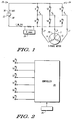
FIG. 1 is a diagram of a system that could utilize the embodiments of the present invention, the system having a power source, an inverter or switching circuit, and a three-phase motor; -
FIG. 2 is a diagram of a controller for the system inFIG. 1 for generating signals to a plurality of switching devices; -
FIG. 3 is a table reflecting the eight possible switching states for a three-phase power device; -
FIG. 4 is top view of one embodiment of a switching circuit and current sensor mounted on a printed circuit board; -
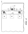
FIG. 5 is top view of one embodiment of an embedded second layer of the printed circuit board inFIG. 4 ; -
FIG. 6 is top view of one embodiment of a switching circuit and current sensor mounted on a printed circuit board; and -
FIG. 7 is top view of one embodiment of an embedded third layer of the printed circuit board inFIG. 6 . -
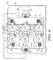
FIG. 8 is top view of another embodiment of a switching circuit and current sensor mounted on a printed circuit board; -
FIG. 9 is top view of another embodiment of an embedded second layer of the printed circuit board inFIG. 8 ; -
FIG. 10 is top view of another embodiment of a switching circuit and current sensor mounted on a printed circuit board; and -
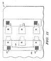
FIG. 11 is top view of another embodiment of an embedded third layer of the printed circuit board inFIG. 10 . - While the invention is susceptible to various modifications and alternative forms, specific embodiments have been shown by way of example in the drawings and will be described in detail herein. However, it should be understood that the invention is not intended to be limited to the particular forms disclosed. Rather, the invention is to cover all modifications, equivalents and alternatives falling within the spirit and scope of the invention as defined by the appended claims.
- What is described is a design for implementing a switching circuit for a three-phase power device on a printed circuit board. The present invention uses embedded directional impedance control channels to balance the resistive and reactive impedance that occur when applying the switching circuit in a printed circuit board application. For purposes of illustration and description, an example of an application for a three-phase motor for automotive uses will be used. Three-phase motors, such as permanent magnet synchronous motors, may be used as part of a power steering system in an automobile. The present invention, however, is not limited to three-phase motors for automobiles and may be applicable to other three-phase devices.
- To this end, generally, there is a printed circuit board for a three-phase power device. The printed circuit board has a first switching device, a second switching device, a third switching device, and a common source node that are each mounted to a surface of the printed circuit board. The printed circuit board further includes at least a first set of conductive paths in a first layer, a second set of conductive paths in a second layer, and a plurality of vias that connects the first layer to the second layer. The first set of conductive paths provides electrical conductivity between the common source node, the first switching device, the second switching device, and third switching device. The second set of conductive paths in the second layer provide electrical conductivity between the common source node, the first switching device, and the third switching device. In this embodiment, the physical distance between the first low side switching device and the common source node and the distance between the third low side switching device and the common source node is greater than a distance between the second low side switching device and the common source node.
- The present invention may be applied to a set of low side switching device and/or to a set of high side switching devices. Accordingly, in one embodiment, the switching devices are low side switching devices and the common source node may include a current sensor. In another embodiment, the switching devices are high side switching devices and the common source node may include a power source node.
- In a further embodiment, there is a printed circuit board for a three-phase power device that has at least a first low side switching device, a second low side switching device, a third low side switching device, and a current sensor that are each mounted to a surface of the printed circuit board. The printed circuit, in one embodiment, has a first set of conductive paths in a first layer, a second set of conductive paths in a second layer, and a plurality of vias. The first set of conductive paths in the first layer of the printed circuit board provides electrical conductivity between the low side switching devices and the current sensor. The second set of conductive paths in the second layer of the printed circuit board provides electrical conductivity between the first low side switching device and the third low side switching device and the current sensor. The plurality of vias connect the first layer to the second layer of the printed circuit board. In this embodiment, the physical distance between the first low side switching device and the current sensor and the distance between the third low side switching device and the current sensor is greater than a distance between the second low side switching device and the current sensor. The printed circuit board may further have a third set of conductive paths in a third layer and a second plurality of vias. The third set of conductive paths in the third layer provides electrical conductivity between the first low side switching device and the third low side switching device.
- In another embodiment, there is a printed circuit board for a three-phase power device having a switching circuit and a current sensor mounted on a surface of the printed circuit board. The switching circuit has three sets of switching devices where each set includes a high side switching device and a low side switching device. The printed circuit board comprises a first set of conductive paths in a first layer, a second set of conductive paths in a second layer, and a plurality of vias. The first set of conductive paths in the first layer of the printed circuit board provides electrical conductivity between each of the low side switching devices in the switching circuit and the current sensor. The second set of conductive paths in the second layer of the printed circuit board provides electrical conductivity between at least two of the low side switching devices of the switching circuit and the current sensor. The plurality of vias connects the first layer of the printed circuit board to the second layer of the printed circuit board. The second conductive paths assist in substantially balancing impedances between the low side switching devices of the switching circuit and the current sensor. The printed circuit board may further have a third set of conductive paths in a third layer and a second plurality of vias. The third set of conductive paths in the third layer provides electrical conductivity between at least two of the low side switching devices of the switching circuit.
- There is also a printed circuit board for a three-phase power device that has at least a first low side switching device, a second low side switching device, a third low side switching device, and a current sensor, each mounted to a surface of the printed circuit board. Here, the printed circuit board comprises a first set of conductive paths in a first layer, a second set of conductive paths in a second layer, a third set of conductive paths in a third layer, and a first and second set of vias. The first set of conductive paths in the first layer of the printed circuit board provides electrical conductivity between the low side switching devices and the current sensor. The second set of conductive paths in the second layer of the printed circuit board provides electrical conductivity between the first low side switching device, the third low side switching device and the current sensor. The third set of conductive paths in the third layer of the printed circuit board provides electrical conductivity between the first low side switching device and the third low side switching device. The first set of vias connect the first layer of the printed circuit board to the second layer of the printed circuit board. The second set of vias connect the first layer of the printed circuit board'to the third layer of the printed circuit board.
- In yet another embodiment, there is a printed circuit board that has a power source node, a first high side switching device, a second high side switching device, and a third high side switching device that are each mounted on the printed circuit board. The printed circuit board further includes at least a first set of conductive paths in a first layer, a second set of conductive paths in a second layer, and a plurality of vias that connect the first layer to the second layer. Here, the first set of conductive paths in the first layer provide electrical conductivity between the power source node, the first high side switching device, the second high side switching device, and the third high side switching device. The second set of conductive paths in the second layer provide electrical conductivity between the power source node, the first high side switching device, and the third high side switching device. The physical distance between the power source node and the first high side switching device and the distance between the power source node and the third high side switching device is greater than a distance between the power source node and the second high side switching device.
- Now, turning to the drawings, an example use of a system for a three-phase motor in an automotive application will be explained. Referring to
FIG. 1 , there is asystem 20 having generally apower source 22, an inverter or switchingcircuit 24, acurrent sensor 26, and amotor 28. For automotive use, thepower source 22 may be an automobile DC battery having apositive terminal 30 and anegative terminal 32. Thenegative terminal 32 may also be a ground connection. Themotor 28 may be a motor having three phase windings A, B, C in a star connection, although other connection types may be used such as a delta connected motor. Such motors may include, for example, a permanent magnet synchronous motor or an induction motor. - The inverter or switching
circuit 24 and the current sensor may be mounted on a surface of a printed circuit board, as will be explained in more detail below. The inverter or switchingcircuit 24 includes three sets of switching devices, one set for each phase winding of themotor 28. A first set of switching devices S1, S2 are capable of providing a first voltage Va to the first phase winding A. A second set of switching devices S3, S4 are capable of providing a second voltage Vb to the second phase winding B. A third set of switching devices S5, S6 are capable of providing a third voltage Vc to the third phase winding C. - In one embodiment, each set of switching devices has a high side switching device S1, S3, S5 connected to the
positive terminal 30 of thepower source 22 and a low side switching device S2, S4, S6 connected to thenegative terminal 32 of the power source 22 (or a ground connection). Each switching device within a set is complimentary to the other switch within the same set. For example, when the high side switching device S1 of the first set of switching devices S1, S2 is closed, the corresponding low side switching device S2 within the first set of switching devices S1, S2 is open. Similarly, when the high side switching device S1 of the first set of switching devices S1, S2 is open, the corresponding low side switching device S2 within the first set of switching devices S1, S2 is closed. - By having complementary switching devices, the opening and closing of switching devices within each set allows each phase winding A, B, C of the
motor 28 to be connected to apositive terminal 30 or a negative terminal 32 (or ground) of thepower supply 22. This permits a voltage Va, Vb, or Vc to be applied to a corresponding phase winding A, B, or C of themotor 28, respectively. The current flowing through each phase winding A, B, or C is represented inFIG. 1 by a corresponding variable i_a, i_b, or i_c, respectively. - As will be explained in more detail below, in one embodiment, the switching devices S1-S6 may be field effect transistors (FETs), each having a source terminal, a drain terminal, and a gate terminal. The FET can be used as a switch by raising and lowering the voltage applied to the gate terminal above and below a threshold value. Applying a voltage above a threshold value will allow current to pass through a switching device S1-S6. Other suitable types of devices exist for the switching devices S1-S6 such as power transistors like IGBT, power MOSFET, and bipolar.
- Pulse width modulated (PWM) signals may be used to control the switching devices S1-S6. Referring to
FIG. 2 , a controller 36 is used to generate a PWM signal to each of the switching devices S1-S6. The controller 36 generates the PWM signal based on the current measurements provided by thecurrent sensor 26. The controller 36 may include a digital processor and memory to store software having control algorithms. The digital processor supplies the PWM signals based the control algorithms implemented in software. A suitable controller 36 may include a DSP processor and memory (not shown). - Referring back to
FIG. 1 , to adequately control themotor 28, the currents for variables i_a, i_b, i_c need to be measured or otherwise known. In one embodiment, thecurrent sensor 26 is positioned on the DC link between thepower supply 22 and the switchingcircuit 24. In particular, thecurrent sensor 26 is located between the low side switching devices S2, S4, S6 of the switchingcircuit 24 and thenegative terminal 30 of thepower supply 22. Thecurrent sensor 26 may also be positioned between the low side switching devices S2, S4, S6 of switchingcircuit 24 and a ground connection. In either event, thecurrent sensor 26 is electrically connected to the low side switching devices S2, S4, S6 of the switchingcircuit 24. The present invention is directed to balancing the resistive and reactive impedances in this electrical connection when the switchingcircuit 24 and thecurrent sensor 26 are implemented on, or mounted to, a surface of a printed circuit board. - The
current sensor 26 may be a sensor that measures the voltage drop across a resistor. Thecurrent sensor 26 may be capable of converting the measured voltage drop to a current (represented by i_de_link) through the DC link according to well-known methods. Alternatively, the measured voltage drop fromsensor 26 may be provided to the controller 36 and the controller 36 may convert the sensed voltage drop to a current. - As explained above, each switching device within a set of switching devices is complementary to the other switching device. For a three-phase motor system, this results in eight possible switching states. The table illustrated in
FIG. 3 reflects the eight possible switching states as vectors V0-V7. Thefirst column 40 in the table represents the states (open/closed) of the first set of switching devices S1, S2. Thesecond column 42 in the table represents the states (open/closed) of the second set of switching devices S3, S4. Thethird column 44 in the table represents the states (open/closed) of the third set of switching devices S5, S6. Thefourth column 46 reflects the relationship between the current through the DC link (i_dc_link) and the currents i_a, i_b, and i_c through the various phase windings A, B, and C. Thefifth column 48 reflects the eight vector states. Out of the eight possible switching states, there are six active vector states (V1-V6) where current will flow through the DC link and two zero vector states (V0, V7) where no current will flow through the DC link. - As mentioned above, the application of sinusoidal drive voltages to a three-phase power device, such as a motor, is subject to torque ripple harmonics. The problem of torque ripple harmonics needs to be addressed when attempting to implement the switching
circuit 24 and thecurrent sensor 26 in a printed circuit board layout. It has been found that torque ripple harmonics will result when resistive and reactive impedances are not balanced. The present invention addresses ways to eliminate, or at least substantially reduce, the effect of the torque ripple harmonics. - Referring to
FIG. 4 , there is shown a printedcircuit board 50 for a three-phase power device, such as themotor 28 described above. The printedcircuit board 50 has a switchingcircuit 24 and acurrent sensor 26 mounted on asurface 52 of the printedcircuit board 50. The switchingcircuit 24 has three sets of switching devices. Each set of switching devices has a high side switching device S1, S3, S5 and a low side switching device S2, S4, S6. - In this embodiment, the
positive terminal 30 of thepower source 22 is connected to the high side switching devices S1, S3, S5 through a powersupply conductive pad 54. The powersupply conductive pad 54 may actually supply power to the high side switching devices S1, S3, S5 through multiple layers in the printed circuit board. This may be important if the current required to drive the three-phase power device is relatively high. The multiple layers may be electrically tied together through vias (not shown). - Each set of switching devices is connected to each other through a series of interconnecting
pads first interconnecting pad 56A provides electrical contact between a first high side switching device S1 and a first low side switching device S2. Asecond interconnecting pad 56B provides electrical contact between a second high side switching device S3 and a second low side switching device S4. Athird interconnecting pad 56C provides electrical contact between a third high side switching device S5 and a third low side switching device S6. - In one embodiment, where the high side switching devices S1, S3, S5 are field effect transistors (FETs), each device has three terminals including a
drain terminal source terminal gate terminal drain terminals supply conductive pad 54. Thesource terminals pads gate terminals - The low side switching device S2, S4, S6 may be connected to the
current sensor 26 by a set ofconductive paths 76 through a commonconductive pad 64. Here, the commonconductive pad 64 may be part of a firstconductive copper layer 78 of the printedcircuit board 50 between the low side switching devices S2, S4, S6 and thecurrent sensor 26. In an embodiment where the low side switching devices S2, S4, S6 are field effect transistors (FETs), each device has three terminals including adrain terminal source terminal gate terminal drain terminals pads source terminals conductive pad 64. And, thegate terminals - The low side switching device S2, S4, S6 (through the current sensor 26) may be connected to the
negative terminal 32 of thepower source 22 through aconductive pad 66. Alternatively, thecurrent sensor 26 may be connected to ground through the sameconductive pad 66. The connection to thenegative terminal 32, or ground connection, may be fed through multiple layers in the printed circuit board. This, again, may be important if the current required to drive the three-phase power device is relatively high. The multiple layers may be electrically tied together through vias (not shown). - Each switching device within a set is complimentary to the other switch within the same set. For example, as mentioned above, when the high side switching device S1 of the first set of switching devices S1, S2 is closed, the corresponding low side switching device S2 within the first set of switching devices S1, S2 is open. Similarly, when the high side switching device S1 of the first set of switching devices S1, S2 is open, the corresponding low side switching device S2 within the first set of switching devices S1, S2 is closed.
- By having complementary switching devices, the opening and closing of switching devices within each set allows each phase winding A, B, C of the
motor 28 to be connected to apositive terminal 30 or a negative terminal 32 (or ground) of thepower supply 22. This is accomplished by having afirst terminal 74A connected between the first high side switching device S1 and the first low side switching device S2, asecond terminal 74B connected between the second high side switching device S3 and the second low side switching device S4, and athird terminal 74C connected between the third high side switching device S5 and the third low side switching device S6. Theterminals motor 28, respectively. The current flowing through each phase winding A, B, or C is represented inFIG. 1 by a corresponding variable i_a, i_b, or i_c, respectively. - The layout of the connection between the
positive terminal 30 of thepower source 22 and the high side switching devices S1, S3, S5 and the connection between thecurrent sensor 26 and thenegative terminal 32 of the power source 22 (or ground) should be highly symmetric and balanced, both physically and electrically. However, in a printed circuit board layout, it is not possible to make the connection between the low side switching devices S2, S4, S6 and thecurrent sensor 26 geometrically symmetric. Moreover, the connection between the low side switching devices S2, S4, S6 themselves are not geometrically symmetric. One aspect of the present invention, as described further below, is directed to mechanisms in making these connections electrically symmetric and balanced to avoid problems associated with torque ripple harmonics. - In the design layout shown in
FIG. 4 , the physical distance between the source terminal 70A of the first low side switching device S2 and thecurrent sensor 26 is greater than the physical distance between the source terminal 70B of the second low side switching device S4 and thecurrent sensor 26. Also, the physical distance between the source terminal 70C of the third low side switching device S6 and thecurrent sensor 26 is greater than the physical distance between the source terminal 70B of the second low side switching device S4 and thecurrent sensor 26. Left with only the commonconductive pad 64 as the electrically connecting member, it has been found that unacceptable torque ripple harmonics will occur during the operation of a three-phase power device. - To solve this problem, in one embodiment, a first set of
vias 80 and a second set ofconductive paths 86 in an embedded secondconductive copper layer 88 of the printed circuit board 50 (as shown inFIG. 5 ) are added to the design. Moreover, the distance between the source terminal 70A of the first low side switching device S2 and thecurrent sensor 26 is set to about twice the distance between the source terminal 70B of the second low side switching device S4 and thecurrent sensor 26. Moreover, the distance between the source terminal 70A of the first low side switching device S2 and thecurrent sensor 26 is set to about twice the distance between the source terminal 70B of the second low side switching device S4 and thecurrent sensor 26. - The physical distances between the low side switching devices S2, S4, S6 and the
current sensor 26 are directly proportional to circuit resistance and impedance. In the printed circuit board layout inFIG. 4 , with only the commonconductive pad 64, the voltage loss associated with the second low side switching device S4 would be less than the losses associated with the first and third low side switching devices S2, S6. The addition of the first set ofvias 80 and the secondconductive paths 86 in thesecond layer 88 of the printed circuit board 50 (as shown inFIG. 5 ) provides a more balanced set of electrical paths between the low side switching devices S2, S4, S6 and thecurrent sensor 26. The first set ofvias 80 stitches, or otherwise connects, thefirst layer 78 to thesecond layer 88. The first set ofvias 80 should be placed at unique points or regions as shown inFIGS. 4-5 . These points or regions are in proximity of the first low side switching device S2, the third low side switching device S6, and thecurrent sensor 26. - Referring to
FIG. 5 , in effect, the use of the first set ofvias 80 adds a second parallel current path between first low side switching device S2 and thecurrent sensor 26 and between the third low side switching device S6 and thecurrent sensor 26. This design helps eliminate, or at least substantially reduce, the effect of torque ripple harmonics. - Referring to the design layout in
FIG. 6 , the commonconductive pad 64 also provides a first set ofconductive paths 77 in thefirst layer 78 of the printedcircuit board 50 when current is fed between the low side switching devices S2, S4, S6 themselves. It is noted that the physical distance between the source terminal 70A of the first low side switching device S2 and the source terminal 70C of the third low side switching device S6 is greater than the physical distance between the source terminal 70A of the first low side switching device S2 and the source terminal 70B of the second low side switching device S4. Also, the physical distance between the source terminal 70C of the third low side switching device S6 and the source terminal 70A of the first low side switching device S2 is greater than the physical distance between the source terminal 70C of the third low side switching device S6 and source terminal 70B of the second low side switching device S4. Again, left with only the commonconductive pad 64 as the electrically connecting member, it has been found that unacceptable torque ripple harmonics will occur during the operation of a three-phase power device. - To solve this problem, in one embodiment, a second set of
vias 90 and a third set ofconductive paths 97 in an embedded thirdconductive copper layer 98 of the printed circuit board 50 (as shown inFIG. 7 ) are added to the design. Moreover, the distance between the source terminal 70A of the first low side switching device S2 and source terminal 70C of the third low side switching device S6 is set to about twice the distance between the source terminal 70A of the first low side switching device S2 and the source terminal 70B of the second low side switching device S4. Moreover, the distance between the source terminal 70C of the third low side switching device S6 and the source terminal 70A of the first low side switching device S2 is set to about twice the distance between the source terminal 70C of the third low side switching device S6 and the source terminal 70B of the second low side switching device S4. - The physical distances between the low side switching devices S2, S4, S6 are directly proportional to circuit resistance and impedance. In the printed circuit board layout in
FIG. 6 , with only the commonconductive pad 64, the voltage loss associated with current between some switching devices would be less than the losses associated between other switching devices. The addition of the second set ofvias 90 and the thirdconductive paths 97 in thethird layer 98 of the printed circuit board 50 (as shown inFIG. 7 ) provides a more balanced set of electrical paths between the low side switching devices S2, S4, S6. The second set ofvias 90 stitches, or otherwise connects, thefirst layer 78 to thethird layer 98. The second set ofvias 90 must be placed at unique points or regions as shown inFIGS. 6-7 . These points or regions are in proximity of the first low side switching device S2 and the third low side switching device S6. - Referring to
FIG. 7 , in effect, the use of the second set ofvias 90 adds a second parallel current path between first low side switching device S2 and the third low side switching device S6. This design helps eliminate, or at least substantially reduce, the effect of torque ripple harmonics. -
FIG. 8 shows another embodiment where the present invention is applied to the high side switching devices S1, S3, S5. This embodiment addresses a potential need for current to funnel evenly out of one power source node, as well as evenly connect to each other when there are recirculating currents between any two of the switching devices. Accordingly,FIG. 8 shows a layout of the connection between thepositive terminal 30 of thepower source 22 and the high side switching devices S1, S3, S5 through apower source node 166 where the connection is not geometrically symmetric. An aspect of the present invention, as described further below, is directed to mechanisms in making these connections electrically symmetric and balanced to avoid problems associated with torque ripple harmonics. - In the design layout shown in
FIG. 8 , the physical distance between apower source node 166 and the first high side switching device S1 is greater than the physical distance between thepower source node 166 and the second high side switching device S3. Also, the physical distance between thepower source node 166 and the third high side switching device S5 is greater than the physical distance between thepower source node 166 and the second high side switching device S3. Left with only a commonconductive pad 154 as the electrically connecting member, unacceptable torque ripple harmonics may occur during the operation of a three-phase power device. - To solve this problem, in one embodiment, a first set of
vias 180 and a second set ofconductive paths 186 in an embedded secondconductive copper layer 188 of the printed circuit board 150 (as shown inFIG. 9 ) are added to the design. Moreover, the distance between thesource node 166 and the first high side switching device S I is set to about twice the distance between thesource node 166 and the second high side switching device S3. Moreover, the distance between thesource node 166 and the third high side switching device S5 is set to about twice the distance between thesource node 166 and the second high side switching device S3. - The physical distances between the
source node 166 and the high side switching devices S1, S3, S5 are directly proportional to circuit resistance and impedance. In the printed circuit board layout inFIG. 8 , with only the commonconductive pad 154, the voltage loss associated with the second high side switching device S3 would be less than the losses associated with the first and third high side switching devices S1, S5. The addition of the first set ofvias 180 and the secondconductive paths 186 in thesecond layer 188 of the printed circuit board 150 (as shown inFIG. 9 ) provides a more balanced set of electrical paths between thesource node 166 and the high side switching devices S1, S3, S5. The first set ofvias 180 stitches, or otherwise connects, thefirst layer 178 to thesecond layer 188. The first set ofvias 180 should be placed at unique points or regions as shown inFIGS. 8-9 . These points or regions are in proximity of the first high side switching device S1, the third high side switching device S5, and thesource node 166. - Referring to
FIG. 9 , in effect, the use of the first set ofvias 180 adds a second parallel current path between thesource node 166 and the first high side switching device S1 and between thesource node 166 and the third high side switching device S5. This design helps eliminate, or at least substantially reduce, the effect of torque ripple harmonics. - Referring to the design layout in
FIG. 10 , the commonconductive pad 154 also provides a first set ofconductive paths 177 in thefirst layer 178 of the printedcircuit board 150 when current is fed between the high side switching devices S1, S3, S5 themselves. It is noted that the physical distance between thedrain terminal 58A of the first high side switching device S1 and thedrain terminal 58C of the third high side switching device S5 is greater than the physical distance between thedrain terminal 58A of the first high side switching device S1 and thedrain terminal 58B of the second high side switching device S3. Also, the physical distance between thedrain terminal 58C of the third high side switching device S5 and thedrain terminal 58A of the first high side switching device S1 is greater than the physical distance between thedrain terminal 58C of the third high side switching device S5 and drain terminal 58B of the second high side switching device S3. Again, left with only the commonconductive pad 154 as the electrically connecting member, unacceptable torque ripple harmonics may occur during the operation of a three-phase power device. - To solve this problem, in one embodiment, a second set of
vias 190 and a third set ofconductive paths 197 in an embedded thirdconductive copper layer 198 of the printed circuit board 150 (as shown inFIG. 11 ) are added to the design. Moreover, the distance between thedrain terminal 58A of the first high side switching device S1 and drain terminal 58C of the third high side switching device S5 is set to about twice the distance between thedrain terminal 58A of the first high side switching device S1 and thedrain terminal 58B of the second high side switching device S3. Moreover, the distance between thedrain terminal 58C of the third high side switching device S5 and thedrain terminal 58A of the first high side switching device S1 is set to about twice the distance between thedrain terminal 58C of the third high side switching device S5 and thedrain terminal 58B of the second high side switching device S3. - The physical distances between the high side switching devices S1, S3, S5 are directly proportional to circuit resistance and impedance. In the printed circuit board layout in
FIG. 10 , with only the commonconductive pad 154, the voltage loss associated with current between some switching devices would be less than the losses associated between other switching devices. The addition of the second set ofvias 190 and the thirdconductive paths 197 in thethird layer 198 of the printed circuit board 150 (as shown inFIG. 11 ) provides a more balanced set of electrical paths between the high side switching devices S1, S3, S5. The second set ofvias 190 stitches, or otherwise connects, thefirst layer 178 to thethird layer 198. The second set ofvias 190 must be placed at unique points or regions as shown inFIGS. 10-11 . These points or regions are in proximity of the first high side switching device S1 and the third high side switching device S5. - Referring to
FIG. 11 , in effect, the use of the second set ofvias 190 adds a second parallel current path between first high side switching device S1 and the third high side switching device S5. This design helps eliminate, or at least substantially reduce, the effect of torque ripple harmonics. - What has been described is an improved procedure for implementing a switching circuit and current sensor on a printed circuit board for three-phase power devices. The above-described system provides a way to optimize, or otherwise balance, the resistive and reactive impedances in the system. In particular, the printed circuit board has multiple conductive paths in embedded layers that serve as directional impedance control channels. This balance helps eliminate, or substantially reduce, the effects of torque ripple harmonics. The design is particularly important in automotive applications where a balanced system is needed to provide power to a three-phase motor for power steering. The present invention solves undesirable oscillations that may occur when a driver is turning the steering wheel.
- The above description of the present invention is intended to be exemplary only and is not intended to limit the scope of any patent issuing from this application. For example, the present discussion used a three-phase motor for automobile applications. The present invention is also applicable to other three-phase devices where pulse width modulation is used. The present invention is intended to be limited only by the scope of the following claims.
Claims (10)
- A printed circuit board for a three-phase power device, the printed circuit board having at least a first switching device, a second switching device, a third switching device, and a common source node that are each mounted to a surface of the printed circuit board, the printed circuit board comprising:a first set of conductive paths in a first layer of the printed circuit board that provides electrical conductivity between the common source node, the first switching device, the second switching device, and the third switching device;a second set of conductive paths in a second layer of the printed circuit board that provides electrical conductivity between the common source node, the first switching device, and the third switching device; anda plurality of vias that connect the first layer of the printed circuit board to the second layer of the printed circuit board wherein said plurality of vias are placed in proximity of the first switching device, the third switching device and the common source node;wherein a distance between the common source node and the first switching device and a distance between the common source node and the third switching device is greater than a distance between the common source node and the second switching device.
- The printed circuit board of claim 1 further comprising:a third set of conductive paths in a third layer of the printed circuit board that provides electrical conductivity between the first switching device and the third switching device; anda second plurality of vias that connect the first layer of the printed circuit board to the third layer of the printed circuit board.
- The printed circuit board of claim 2 wherein a portion of the second plurality of vias is the same as the first plurality of vias.
- The printed circuit board of claim 1 wherein the first switching device is a first low side switching device, the second switching device is a second low side switching device, and the third switching device is a third low side switching device.
- The printed circuit board of claim 4 wherein the common source node comprises a current sensor.
- The printed circuit board of claim 4 further having at least a first high side switching device, a second high side switching device, and a third high side switching device that are each mounted to a surface of the printed circuit board, the printed circuit board further comprising:a first terminal connected between the first high side switching device and the first low side switching device, the first terminal providing power to a first phase winding of the three-phase power device;a second terminal connected between the second high side switching device and the second low side switching device, the second terminal providing power to a second phase winding of the three-phase power device; anda third terminal connected between the third high side switching device and the third low side switching device, the third terminal providing power to a third phase winding of the three-phase power device.
- The printed circuit board of claim 1 wherein the first switching device is a first high side switching device, the second switching device is a second high side switching device, and the third switching device is a third high side switching device.
- The printed circuit board of claim 7 wherein the common source node comprises a power source node.
- The printed circuit board of claim 7 further having at least a first low side switching device, a second low side switching device, and a third low side switching device that are each mounted to a surface of the printed circuit board, the printed circuit board further comprising:a first terminal connected between the first high side switching device and the first low side switching device, the first terminal providing power to a first phase winding of the three-phase power device;a second terminal connected between the second high side switching device and the second low side switching device, the second terminal providing power to a second phase winding of the three-phase power device; anda third terminal connected between the third high side switching device and the third low side switching device, the third terminal providing power to a third phase winding of the three-phase power device.
- The printed circuit board of claim 1 wherein the distance between the common source node and the first switching device is about twice the distance between the common source node and the second switching device.
Applications Claiming Priority (3)
| Application Number | Priority Date | Filing Date | Title |
|---|---|---|---|
| US48587403P | 2003-07-09 | 2003-07-09 | |
| US10/721,030 US7154196B2 (en) | 2003-07-09 | 2003-11-24 | Printed circuit board for a three-phase power device having embedded directional impedance control channels |
| PCT/US2004/019247 WO2005011342A2 (en) | 2003-07-09 | 2004-06-17 | Embedded directional impedance control channels for pc boards |
Publications (3)
| Publication Number | Publication Date |
|---|---|
| EP1645023A2 EP1645023A2 (en) | 2006-04-12 |
| EP1645023A4 EP1645023A4 (en) | 2009-07-01 |
| EP1645023B1 true EP1645023B1 (en) | 2011-06-15 |
Family
ID=34107724
Family Applications (1)
| Application Number | Title | Priority Date | Filing Date |
|---|---|---|---|
| EP04776671A Expired - Lifetime EP1645023B1 (en) | 2003-07-09 | 2004-06-17 | Printed circuit board for a three-phase power device having embedded directional impedance control channels |
Country Status (5)
| Country | Link |
|---|---|
| US (1) | US7154196B2 (en) |
| EP (1) | EP1645023B1 (en) |
| JP (1) | JP4286861B2 (en) |
| AT (1) | ATE513354T1 (en) |
| WO (1) | WO2005011342A2 (en) |
Cited By (2)
| Publication number | Priority date | Publication date | Assignee | Title |
|---|---|---|---|---|
| US9711778B2 (en) | 2013-09-06 | 2017-07-18 | Johnson Controls Technology Company | Layered battery module system and method of assembly |
| CN110168911A (en) * | 2017-01-11 | 2019-08-23 | 东芝三菱电机产业系统株式会社 | Power-converting device |
Families Citing this family (5)
| Publication number | Priority date | Publication date | Assignee | Title |
|---|---|---|---|---|
| US8089776B2 (en) * | 2006-06-19 | 2012-01-03 | Sony Ericsson Mobile Communications Ab | Side switch for a contact exposed on an edge of a circuit board and method |
| JP4977165B2 (en) * | 2009-04-01 | 2012-07-18 | トヨタ自動車株式会社 | Noise reduction structure for 3-phase brushless motor |
| DE102011008952A1 (en) | 2011-01-19 | 2012-07-19 | Texas Instruments Deutschland Gmbh | Multi-chip module, method of operating the same and DC / DC converter |
| JP6922175B2 (en) * | 2016-09-01 | 2021-08-18 | 富士電機株式会社 | Power converter |
| WO2019056072A1 (en) | 2017-09-22 | 2019-03-28 | Janislav Sega | System and method for controlling a motor |
Family Cites Families (18)
| Publication number | Priority date | Publication date | Assignee | Title |
|---|---|---|---|---|
| JPS63314177A (en) * | 1987-06-16 | 1988-12-22 | Mitsubishi Electric Corp | Inverter apparatus |
| US5519633A (en) * | 1993-03-08 | 1996-05-21 | International Business Machines Corporation | Method and apparatus for the cross-sectional design of multi-layer printed circuit boards |
| US5528073A (en) * | 1994-07-05 | 1996-06-18 | Allen-Bradley Company, Inc. | Bus bar having reduced parasitic inductances and equal current path lengths |
| US5532512A (en) * | 1994-10-03 | 1996-07-02 | General Electric Company | Direct stacked and flip chip power semiconductor device structures |
| US5956231A (en) * | 1994-10-07 | 1999-09-21 | Hitachi, Ltd. | Semiconductor device having power semiconductor elements |
| US5641944A (en) * | 1995-09-29 | 1997-06-24 | Allen-Bradley Company, Inc. | Power substrate with improved thermal characteristics |
| US5682298A (en) * | 1996-06-13 | 1997-10-28 | Hewlett-Packard Company | Balancing power distribution in a power supply system with redundant power sources |
| US5912809A (en) * | 1997-01-21 | 1999-06-15 | Dell Usa, L.P. | Printed circuit board (PCB) including channeled capacitive plane structure |
| US6462976B1 (en) * | 1997-02-21 | 2002-10-08 | University Of Arkansas | Conversion of electrical energy from one form to another, and its management through multichip module structures |
| JPH11177189A (en) * | 1997-12-12 | 1999-07-02 | Fujitsu Ltd | Termination structure of wiring on printed circuit board |
| US6072699A (en) * | 1998-07-21 | 2000-06-06 | Intel Corporation | Method and apparatus for matching trace lengths of signal lines making 90°/180° turns |
| US6356162B1 (en) * | 1999-04-02 | 2002-03-12 | Nordx/Cdt, Inc. | Impedance compensation for a cable and connector |
| JP2000102253A (en) * | 1998-09-25 | 2000-04-07 | Hitachi Ltd | Power converter |
| US6194990B1 (en) * | 1999-03-16 | 2001-02-27 | Motorola, Inc. | Printed circuit board with a multilayer integral thin-film metal resistor and method therefor |
| JP3819195B2 (en) * | 1999-11-12 | 2006-09-06 | 三菱電機株式会社 | Power module |
| US7012811B1 (en) * | 2000-05-10 | 2006-03-14 | Micron Technology, Inc. | Method of tuning a multi-path circuit |
| JP2002320391A (en) * | 2001-04-19 | 2002-10-31 | Fuji Electric Co Ltd | Conductor structure of large-capacity power converter |
| US20040061241A1 (en) * | 2002-09-30 | 2004-04-01 | Osburn Edward P. | Semiconductor device power interconnect striping |
-
2003
- 2003-11-24 US US10/721,030 patent/US7154196B2/en not_active Expired - Fee Related
-
2004
- 2004-06-17 EP EP04776671A patent/EP1645023B1/en not_active Expired - Lifetime
- 2004-06-17 AT AT04776671T patent/ATE513354T1/en not_active IP Right Cessation
- 2004-06-17 JP JP2006518652A patent/JP4286861B2/en not_active Expired - Fee Related
- 2004-06-17 WO PCT/US2004/019247 patent/WO2005011342A2/en not_active Ceased
Cited By (4)
| Publication number | Priority date | Publication date | Assignee | Title |
|---|---|---|---|---|
| US9711778B2 (en) | 2013-09-06 | 2017-07-18 | Johnson Controls Technology Company | Layered battery module system and method of assembly |
| US10511006B2 (en) | 2013-09-06 | 2019-12-17 | Cps Technology Holdings Llc | Layered battery module system and method of assembly |
| CN110168911A (en) * | 2017-01-11 | 2019-08-23 | 东芝三菱电机产业系统株式会社 | Power-converting device |
| CN110168911B (en) * | 2017-01-11 | 2021-02-09 | 东芝三菱电机产业系统株式会社 | Power conversion device |
Also Published As
| Publication number | Publication date |
|---|---|
| JP2007527684A (en) | 2007-09-27 |
| US20050035816A1 (en) | 2005-02-17 |
| JP4286861B2 (en) | 2009-07-01 |
| WO2005011342A2 (en) | 2005-02-03 |
| EP1645023A2 (en) | 2006-04-12 |
| ATE513354T1 (en) | 2011-07-15 |
| US7154196B2 (en) | 2006-12-26 |
| EP1645023A4 (en) | 2009-07-01 |
| WO2005011342A3 (en) | 2005-04-28 |
Similar Documents
| Publication | Publication Date | Title |
|---|---|---|
| US8829746B2 (en) | Controller for an electric motor | |
| US11489437B2 (en) | DC inverter/converter current balancing for paralleled phase leg switches | |
| US9123711B2 (en) | Wiring member and semiconductor module having the same | |
| US20130119908A1 (en) | Electronic control unit for electric power steering | |
| WO2019098217A1 (en) | Inverter control board | |
| CN102835015B (en) | Inverter unit | |
| US20200382047A1 (en) | Electric power steering device | |
| US7154196B2 (en) | Printed circuit board for a three-phase power device having embedded directional impedance control channels | |
| US7671639B2 (en) | Electronic circuit | |
| US6266258B1 (en) | Power substrate element topology | |
| US10886862B2 (en) | Semiconductor device | |
| JPH10304679A (en) | Wiring construction body and inverter unit | |
| JP2005278296A (en) | Capacitor device and power supply system having the same | |
| JP2002136154A (en) | Capacitor and inverter device | |
| EP0713251B1 (en) | Semiconductor conversion device | |
| KR101489748B1 (en) | System on chip for power inverter | |
| JP3149648B2 (en) | Semiconductor converter | |
| JPH0947035A (en) | Inverter | |
| JP2025111891A (en) | Control apparatus and power conversion equipment | |
| WO2023095244A1 (en) | Power conversion device | |
| CN112769370A (en) | EPS circuit board | |
| JP2021150978A (en) | Power conversion device | |
| CN88102081A (en) | Inverter | |
| JP2005287236A (en) | Electrical equipment unit |
Legal Events
| Date | Code | Title | Description |
|---|---|---|---|
| PUAI | Public reference made under article 153(3) epc to a published international application that has entered the european phase |
Free format text: ORIGINAL CODE: 0009012 |
|
| 17P | Request for examination filed |
Effective date: 20060123 |
|
| AK | Designated contracting states |
Kind code of ref document: A2 Designated state(s): AT BE BG CH CY CZ DE DK EE ES FI FR GB GR HU IE IT LI LU MC NL PL PT RO SE SI SK TR |
|
| DAX | Request for extension of the european patent (deleted) | ||
| A4 | Supplementary search report drawn up and despatched |
Effective date: 20090604 |
|
| GRAP | Despatch of communication of intention to grant a patent |
Free format text: ORIGINAL CODE: EPIDOSNIGR1 |
|
| GRAS | Grant fee paid |
Free format text: ORIGINAL CODE: EPIDOSNIGR3 |
|
| GRAA | (expected) grant |
Free format text: ORIGINAL CODE: 0009210 |
|
| AK | Designated contracting states |
Kind code of ref document: B1 Designated state(s): AT BE BG CH CY CZ DE DK EE ES FI FR GB GR HU IE IT LI LU MC NL PL PT RO SE SI SK TR |
|
| REG | Reference to a national code |
Ref country code: GB Ref legal event code: FG4D Ref country code: CH Ref legal event code: EP |
|
| REG | Reference to a national code |
Ref country code: IE Ref legal event code: FG4D |
|
| REG | Reference to a national code |
Ref country code: DE Ref legal event code: R096 Ref document number: 602004033101 Country of ref document: DE Effective date: 20110721 |
|
| REG | Reference to a national code |
Ref country code: NL Ref legal event code: VDEP Effective date: 20110615 |
|
| PG25 | Lapsed in a contracting state [announced via postgrant information from national office to epo] |
Ref country code: SE Free format text: LAPSE BECAUSE OF FAILURE TO SUBMIT A TRANSLATION OF THE DESCRIPTION OR TO PAY THE FEE WITHIN THE PRESCRIBED TIME-LIMIT Effective date: 20110615 |
|
| PG25 | Lapsed in a contracting state [announced via postgrant information from national office to epo] |
Ref country code: FI Free format text: LAPSE BECAUSE OF FAILURE TO SUBMIT A TRANSLATION OF THE DESCRIPTION OR TO PAY THE FEE WITHIN THE PRESCRIBED TIME-LIMIT Effective date: 20110615 Ref country code: SI Free format text: LAPSE BECAUSE OF FAILURE TO SUBMIT A TRANSLATION OF THE DESCRIPTION OR TO PAY THE FEE WITHIN THE PRESCRIBED TIME-LIMIT Effective date: 20110615 Ref country code: GR Free format text: LAPSE BECAUSE OF FAILURE TO SUBMIT A TRANSLATION OF THE DESCRIPTION OR TO PAY THE FEE WITHIN THE PRESCRIBED TIME-LIMIT Effective date: 20110916 Ref country code: AT Free format text: LAPSE BECAUSE OF FAILURE TO SUBMIT A TRANSLATION OF THE DESCRIPTION OR TO PAY THE FEE WITHIN THE PRESCRIBED TIME-LIMIT Effective date: 20110615 Ref country code: CY Free format text: LAPSE BECAUSE OF FAILURE TO SUBMIT A TRANSLATION OF THE DESCRIPTION OR TO PAY THE FEE WITHIN THE PRESCRIBED TIME-LIMIT Effective date: 20110615 |
|
| PG25 | Lapsed in a contracting state [announced via postgrant information from national office to epo] |
Ref country code: BE Free format text: LAPSE BECAUSE OF FAILURE TO SUBMIT A TRANSLATION OF THE DESCRIPTION OR TO PAY THE FEE WITHIN THE PRESCRIBED TIME-LIMIT Effective date: 20110615 Ref country code: NL Free format text: LAPSE BECAUSE OF FAILURE TO SUBMIT A TRANSLATION OF THE DESCRIPTION OR TO PAY THE FEE WITHIN THE PRESCRIBED TIME-LIMIT Effective date: 20110615 |
|
| PG25 | Lapsed in a contracting state [announced via postgrant information from national office to epo] |
Ref country code: PT Free format text: LAPSE BECAUSE OF FAILURE TO SUBMIT A TRANSLATION OF THE DESCRIPTION OR TO PAY THE FEE WITHIN THE PRESCRIBED TIME-LIMIT Effective date: 20111017 Ref country code: CZ Free format text: LAPSE BECAUSE OF FAILURE TO SUBMIT A TRANSLATION OF THE DESCRIPTION OR TO PAY THE FEE WITHIN THE PRESCRIBED TIME-LIMIT Effective date: 20110615 Ref country code: EE Free format text: LAPSE BECAUSE OF FAILURE TO SUBMIT A TRANSLATION OF THE DESCRIPTION OR TO PAY THE FEE WITHIN THE PRESCRIBED TIME-LIMIT Effective date: 20110615 |
|
| REG | Reference to a national code |
Ref country code: CH Ref legal event code: PL |
|
| PG25 | Lapsed in a contracting state [announced via postgrant information from national office to epo] |
Ref country code: PL Free format text: LAPSE BECAUSE OF FAILURE TO SUBMIT A TRANSLATION OF THE DESCRIPTION OR TO PAY THE FEE WITHIN THE PRESCRIBED TIME-LIMIT Effective date: 20110615 Ref country code: RO Free format text: LAPSE BECAUSE OF FAILURE TO SUBMIT A TRANSLATION OF THE DESCRIPTION OR TO PAY THE FEE WITHIN THE PRESCRIBED TIME-LIMIT Effective date: 20110615 Ref country code: SK Free format text: LAPSE BECAUSE OF FAILURE TO SUBMIT A TRANSLATION OF THE DESCRIPTION OR TO PAY THE FEE WITHIN THE PRESCRIBED TIME-LIMIT Effective date: 20110615 |
|
| REG | Reference to a national code |
Ref country code: IE Ref legal event code: MM4A |
|
| PLBE | No opposition filed within time limit |
Free format text: ORIGINAL CODE: 0009261 |
|
| STAA | Information on the status of an ep patent application or granted ep patent |
Free format text: STATUS: NO OPPOSITION FILED WITHIN TIME LIMIT |
|
| PG25 | Lapsed in a contracting state [announced via postgrant information from national office to epo] |
Ref country code: IE Free format text: LAPSE BECAUSE OF NON-PAYMENT OF DUE FEES Effective date: 20110617 Ref country code: CH Free format text: LAPSE BECAUSE OF NON-PAYMENT OF DUE FEES Effective date: 20110630 Ref country code: LI Free format text: LAPSE BECAUSE OF NON-PAYMENT OF DUE FEES Effective date: 20110630 Ref country code: FR Free format text: LAPSE BECAUSE OF NON-PAYMENT OF DUE FEES Effective date: 20110816 |
|
| REG | Reference to a national code |
Ref country code: FR Ref legal event code: ST Effective date: 20120330 |
|
| 26N | No opposition filed |
Effective date: 20120316 |
|
| GBPC | Gb: european patent ceased through non-payment of renewal fee |
Effective date: 20110915 |
|
| PG25 | Lapsed in a contracting state [announced via postgrant information from national office to epo] |
Ref country code: IT Free format text: LAPSE BECAUSE OF FAILURE TO SUBMIT A TRANSLATION OF THE DESCRIPTION OR TO PAY THE FEE WITHIN THE PRESCRIBED TIME-LIMIT Effective date: 20110615 |
|
| PG25 | Lapsed in a contracting state [announced via postgrant information from national office to epo] |
Ref country code: DK Free format text: LAPSE BECAUSE OF FAILURE TO SUBMIT A TRANSLATION OF THE DESCRIPTION OR TO PAY THE FEE WITHIN THE PRESCRIBED TIME-LIMIT Effective date: 20110615 |
|
| REG | Reference to a national code |
Ref country code: DE Ref legal event code: R097 Ref document number: 602004033101 Country of ref document: DE Effective date: 20120316 |
|
| PG25 | Lapsed in a contracting state [announced via postgrant information from national office to epo] |
Ref country code: GB Free format text: LAPSE BECAUSE OF NON-PAYMENT OF DUE FEES Effective date: 20110915 |
|
| PG25 | Lapsed in a contracting state [announced via postgrant information from national office to epo] |
Ref country code: MC Free format text: LAPSE BECAUSE OF NON-PAYMENT OF DUE FEES Effective date: 20110630 Ref country code: ES Free format text: LAPSE BECAUSE OF FAILURE TO SUBMIT A TRANSLATION OF THE DESCRIPTION OR TO PAY THE FEE WITHIN THE PRESCRIBED TIME-LIMIT Effective date: 20110926 |
|
| PG25 | Lapsed in a contracting state [announced via postgrant information from national office to epo] |
Ref country code: LU Free format text: LAPSE BECAUSE OF NON-PAYMENT OF DUE FEES Effective date: 20110617 |
|
| PG25 | Lapsed in a contracting state [announced via postgrant information from national office to epo] |
Ref country code: BG Free format text: LAPSE BECAUSE OF FAILURE TO SUBMIT A TRANSLATION OF THE DESCRIPTION OR TO PAY THE FEE WITHIN THE PRESCRIBED TIME-LIMIT Effective date: 20110915 |
|
| PGFP | Annual fee paid to national office [announced via postgrant information from national office to epo] |
Ref country code: DE Payment date: 20130630 Year of fee payment: 10 |
|
| PG25 | Lapsed in a contracting state [announced via postgrant information from national office to epo] |
Ref country code: TR Free format text: LAPSE BECAUSE OF FAILURE TO SUBMIT A TRANSLATION OF THE DESCRIPTION OR TO PAY THE FEE WITHIN THE PRESCRIBED TIME-LIMIT Effective date: 20110615 |
|
| PG25 | Lapsed in a contracting state [announced via postgrant information from national office to epo] |
Ref country code: HU Free format text: LAPSE BECAUSE OF FAILURE TO SUBMIT A TRANSLATION OF THE DESCRIPTION OR TO PAY THE FEE WITHIN THE PRESCRIBED TIME-LIMIT Effective date: 20110615 |
|
| REG | Reference to a national code |
Ref country code: DE Ref legal event code: R119 Ref document number: 602004033101 Country of ref document: DE |
|
| REG | Reference to a national code |
Ref country code: DE Ref legal event code: R119 Ref document number: 602004033101 Country of ref document: DE Effective date: 20150101 |
|
| PG25 | Lapsed in a contracting state [announced via postgrant information from national office to epo] |
Ref country code: DE Free format text: LAPSE BECAUSE OF NON-PAYMENT OF DUE FEES Effective date: 20150101 |