EP1643558A1 - Vertical power semiconductor device and method of making the same - Google Patents
Vertical power semiconductor device and method of making the same Download PDFInfo
- Publication number
- EP1643558A1 EP1643558A1 EP04425733A EP04425733A EP1643558A1 EP 1643558 A1 EP1643558 A1 EP 1643558A1 EP 04425733 A EP04425733 A EP 04425733A EP 04425733 A EP04425733 A EP 04425733A EP 1643558 A1 EP1643558 A1 EP 1643558A1
- Authority
- EP
- European Patent Office
- Prior art keywords
- drain
- source
- gate
- area
- realised
- Prior art date
- Legal status (The legal status is an assumption and is not a legal conclusion. Google has not performed a legal analysis and makes no representation as to the accuracy of the status listed.)
- Granted
Links
Images



Classifications
-
- H—ELECTRICITY
- H10—SEMICONDUCTOR DEVICES; ELECTRIC SOLID-STATE DEVICES NOT OTHERWISE PROVIDED FOR
- H10D—INORGANIC ELECTRIC SEMICONDUCTOR DEVICES
- H10D30/00—Field-effect transistors [FET]
- H10D30/01—Manufacture or treatment
- H10D30/021—Manufacture or treatment of FETs having insulated gates [IGFET]
- H10D30/028—Manufacture or treatment of FETs having insulated gates [IGFET] of double-diffused metal oxide semiconductor [DMOS] FETs
- H10D30/0291—Manufacture or treatment of FETs having insulated gates [IGFET] of double-diffused metal oxide semiconductor [DMOS] FETs of vertical DMOS [VDMOS] FETs
-
- H—ELECTRICITY
- H10—SEMICONDUCTOR DEVICES; ELECTRIC SOLID-STATE DEVICES NOT OTHERWISE PROVIDED FOR
- H10D—INORGANIC ELECTRIC SEMICONDUCTOR DEVICES
- H10D10/00—Bipolar junction transistors [BJT]
- H10D10/01—Manufacture or treatment
- H10D10/051—Manufacture or treatment of vertical BJTs
-
- H—ELECTRICITY
- H10—SEMICONDUCTOR DEVICES; ELECTRIC SOLID-STATE DEVICES NOT OTHERWISE PROVIDED FOR
- H10D—INORGANIC ELECTRIC SEMICONDUCTOR DEVICES
- H10D10/00—Bipolar junction transistors [BJT]
- H10D10/40—Vertical BJTs
- H10D10/421—Vertical BJTs having both emitter-base and base-collector junctions ending at the same surface of the body
-
- H—ELECTRICITY
- H10—SEMICONDUCTOR DEVICES; ELECTRIC SOLID-STATE DEVICES NOT OTHERWISE PROVIDED FOR
- H10D—INORGANIC ELECTRIC SEMICONDUCTOR DEVICES
- H10D12/00—Bipolar devices controlled by the field effect, e.g. insulated-gate bipolar transistors [IGBT]
- H10D12/01—Manufacture or treatment
- H10D12/031—Manufacture or treatment of IGBTs
- H10D12/032—Manufacture or treatment of IGBTs of vertical IGBTs
-
- H—ELECTRICITY
- H10—SEMICONDUCTOR DEVICES; ELECTRIC SOLID-STATE DEVICES NOT OTHERWISE PROVIDED FOR
- H10D—INORGANIC ELECTRIC SEMICONDUCTOR DEVICES
- H10D12/00—Bipolar devices controlled by the field effect, e.g. insulated-gate bipolar transistors [IGBT]
- H10D12/411—Insulated-gate bipolar transistors [IGBT]
- H10D12/441—Vertical IGBTs
- H10D12/491—Vertical IGBTs having both emitter contacts and collector contacts in the same substrate side
-
- H—ELECTRICITY
- H10—SEMICONDUCTOR DEVICES; ELECTRIC SOLID-STATE DEVICES NOT OTHERWISE PROVIDED FOR
- H10D—INORGANIC ELECTRIC SEMICONDUCTOR DEVICES
- H10D30/00—Field-effect transistors [FET]
- H10D30/01—Manufacture or treatment
- H10D30/021—Manufacture or treatment of FETs having insulated gates [IGFET]
- H10D30/025—Manufacture or treatment of FETs having insulated gates [IGFET] of vertical IGFETs
-
- H—ELECTRICITY
- H10—SEMICONDUCTOR DEVICES; ELECTRIC SOLID-STATE DEVICES NOT OTHERWISE PROVIDED FOR
- H10D—INORGANIC ELECTRIC SEMICONDUCTOR DEVICES
- H10D30/00—Field-effect transistors [FET]
- H10D30/60—Insulated-gate field-effect transistors [IGFET]
- H10D30/64—Double-diffused metal-oxide semiconductor [DMOS] FETs
- H10D30/66—Vertical DMOS [VDMOS] FETs
- H10D30/663—Vertical DMOS [VDMOS] FETs having both source contacts and drain contacts on the same surface, i.e. up-drain VDMOS
-
- H—ELECTRICITY
- H10—SEMICONDUCTOR DEVICES; ELECTRIC SOLID-STATE DEVICES NOT OTHERWISE PROVIDED FOR
- H10D—INORGANIC ELECTRIC SEMICONDUCTOR DEVICES
- H10D62/00—Semiconductor bodies, or regions thereof, of devices having potential barriers
- H10D62/10—Shapes, relative sizes or dispositions of the regions of the semiconductor bodies; Shapes of the semiconductor bodies
- H10D62/124—Shapes, relative sizes or dispositions of the regions of semiconductor bodies or of junctions between the regions
- H10D62/126—Top-view geometrical layouts of the regions or the junctions
-
- H—ELECTRICITY
- H10—SEMICONDUCTOR DEVICES; ELECTRIC SOLID-STATE DEVICES NOT OTHERWISE PROVIDED FOR
- H10D—INORGANIC ELECTRIC SEMICONDUCTOR DEVICES
- H10D62/00—Semiconductor bodies, or regions thereof, of devices having potential barriers
- H10D62/10—Shapes, relative sizes or dispositions of the regions of the semiconductor bodies; Shapes of the semiconductor bodies
- H10D62/124—Shapes, relative sizes or dispositions of the regions of semiconductor bodies or of junctions between the regions
- H10D62/126—Top-view geometrical layouts of the regions or the junctions
- H10D62/127—Top-view geometrical layouts of the regions or the junctions of cellular field-effect devices, e.g. multicellular DMOS transistors or IGBTs
-
- H—ELECTRICITY
- H10—SEMICONDUCTOR DEVICES; ELECTRIC SOLID-STATE DEVICES NOT OTHERWISE PROVIDED FOR
- H10D—INORGANIC ELECTRIC SEMICONDUCTOR DEVICES
- H10D64/00—Electrodes of devices having potential barriers
- H10D64/20—Electrodes characterised by their shapes, relative sizes or dispositions
- H10D64/23—Electrodes carrying the current to be rectified, amplified, oscillated or switched, e.g. sources, drains, anodes or cathodes
-
- H—ELECTRICITY
- H10—SEMICONDUCTOR DEVICES; ELECTRIC SOLID-STATE DEVICES NOT OTHERWISE PROVIDED FOR
- H10D—INORGANIC ELECTRIC SEMICONDUCTOR DEVICES
- H10D64/00—Electrodes of devices having potential barriers
- H10D64/20—Electrodes characterised by their shapes, relative sizes or dispositions
- H10D64/23—Electrodes carrying the current to be rectified, amplified, oscillated or switched, e.g. sources, drains, anodes or cathodes
- H10D64/231—Emitter or collector electrodes for bipolar transistors
-
- H—ELECTRICITY
- H10—SEMICONDUCTOR DEVICES; ELECTRIC SOLID-STATE DEVICES NOT OTHERWISE PROVIDED FOR
- H10D—INORGANIC ELECTRIC SEMICONDUCTOR DEVICES
- H10D64/00—Electrodes of devices having potential barriers
- H10D64/20—Electrodes characterised by their shapes, relative sizes or dispositions
- H10D64/23—Electrodes carrying the current to be rectified, amplified, oscillated or switched, e.g. sources, drains, anodes or cathodes
- H10D64/251—Source or drain electrodes for field-effect devices
- H10D64/252—Source or drain electrodes for field-effect devices for vertical or pseudo-vertical devices
-
- H—ELECTRICITY
- H10—SEMICONDUCTOR DEVICES; ELECTRIC SOLID-STATE DEVICES NOT OTHERWISE PROVIDED FOR
- H10D—INORGANIC ELECTRIC SEMICONDUCTOR DEVICES
- H10D64/00—Electrodes of devices having potential barriers
- H10D64/20—Electrodes characterised by their shapes, relative sizes or dispositions
- H10D64/23—Electrodes carrying the current to be rectified, amplified, oscillated or switched, e.g. sources, drains, anodes or cathodes
- H10D64/251—Source or drain electrodes for field-effect devices
- H10D64/256—Source or drain electrodes for field-effect devices for lateral devices wherein the source or drain electrodes are recessed in semiconductor bodies
-
- H—ELECTRICITY
- H10—SEMICONDUCTOR DEVICES; ELECTRIC SOLID-STATE DEVICES NOT OTHERWISE PROVIDED FOR
- H10D—INORGANIC ELECTRIC SEMICONDUCTOR DEVICES
- H10D8/00—Diodes
- H10D8/01—Manufacture or treatment
- H10D8/043—Manufacture or treatment of planar diodes
-
- H—ELECTRICITY
- H10—SEMICONDUCTOR DEVICES; ELECTRIC SOLID-STATE DEVICES NOT OTHERWISE PROVIDED FOR
- H10D—INORGANIC ELECTRIC SEMICONDUCTOR DEVICES
- H10D8/00—Diodes
- H10D8/411—PN diodes having planar bodies
-
- H—ELECTRICITY
- H10—SEMICONDUCTOR DEVICES; ELECTRIC SOLID-STATE DEVICES NOT OTHERWISE PROVIDED FOR
- H10D—INORGANIC ELECTRIC SEMICONDUCTOR DEVICES
- H10D62/00—Semiconductor bodies, or regions thereof, of devices having potential barriers
- H10D62/10—Shapes, relative sizes or dispositions of the regions of the semiconductor bodies; Shapes of the semiconductor bodies
- H10D62/13—Semiconductor regions connected to electrodes carrying current to be rectified, amplified or switched, e.g. source or drain regions
- H10D62/149—Source or drain regions of field-effect devices
- H10D62/151—Source or drain regions of field-effect devices of IGFETs
- H10D62/156—Drain regions of DMOS transistors
- H10D62/157—Impurity concentrations or distributions
-
- H—ELECTRICITY
- H10—SEMICONDUCTOR DEVICES; ELECTRIC SOLID-STATE DEVICES NOT OTHERWISE PROVIDED FOR
- H10D—INORGANIC ELECTRIC SEMICONDUCTOR DEVICES
- H10D64/00—Electrodes of devices having potential barriers
- H10D64/20—Electrodes characterised by their shapes, relative sizes or dispositions
- H10D64/23—Electrodes carrying the current to be rectified, amplified, oscillated or switched, e.g. sources, drains, anodes or cathodes
- H10D64/233—Cathode or anode electrodes for thyristors
-
- H—ELECTRICITY
- H10—SEMICONDUCTOR DEVICES; ELECTRIC SOLID-STATE DEVICES NOT OTHERWISE PROVIDED FOR
- H10P—GENERIC PROCESSES OR APPARATUS FOR THE MANUFACTURE OR TREATMENT OF DEVICES COVERED BY CLASS H10
- H10P30/00—Ion implantation into wafers, substrates or parts of devices
- H10P30/20—Ion implantation into wafers, substrates or parts of devices into semiconductor materials, e.g. for doping
- H10P30/222—Ion implantation into wafers, substrates or parts of devices into semiconductor materials, e.g. for doping characterised by the angle between the ion beam and the crystal planes or the main crystal surface
Definitions
- the present invention relates to a vertical conduction electronic power device and corresponding realisation method.
- the present invention relates to a vertical conduction electronic power device being integrated on a semiconductor substrate, comprising gate, source and drain areas, realised in an epitaxial layer on said semiconductor substrate and comprising gate, source and drain lines realised by means of a first metallisation as well as gate, source and drain terminals determined by means of a second metallisation, said drain line being connected to a sinker structure realised in said epitaxial layer.
- the invention relates particularly, but not exclusively, to a MOS vertical conduction power device and the following description is made with reference to this field of application for convenience of illustration only
- the highest ration between the chip or die size and the footprint thereof moved from around 0.3 in the early nineties to around 0.8 at the end of the century.
- FFOM Q-factor
- a first variously developed solution is represented by a power device realised by means of a conveniently shaped metal container or frame suitable to draw at the same level in an upper surface the device conduction terminal (drain) located on a lower surface.
- An embodiment thereof is shown in figure 1 and described in the document MOSFET BGA design - Fairchild Semiconductor - August 2002.
- a method is described for realising a power device comprising an assembly step wherein the device integrated on the semiconductor (die) is welded inside a frame through conventional so-called die attach techniques.
- the solution being provided has the drawback that the levelling of conduction terminals (source, gate) located on the device upper surface with the conduction terminal (drain) located on the opposite surface, and drawn on this surface, is ensured in the absence of the frame mechanical tolerances, of the semiconductor chip thickness as well as of the thickness of the welding compound used for the die attach technique. Therefore this solution is not sufficiently reliable for the realisation of large-scale-efficiency vertical conduction power devices.
- a second known solution provides for the complete removal of the metal frame by realising a package immediately on a silicon chip, whereon a plurality of dies are integrated, before splitting the single dies.
- WLCSP Wafer Level Chip Scale Package
- conduction terminals are drawn on a same device surface.
- This solution provides the realisation of deep sinkers, along the die outer perimeter, crossing the whole silicon chip thickness, which are filled with a conductive material such as a metal (for example gold).
- this second known solution although advantageous under several aspects, has the drawback that the current flow, coming from the terminal located in the die lower surface, can be collected only along the outer perimeter of the device upper surface. This implies that the resistive contribution due to the current flow path on the substrate is considerable. Moreover the provided realisation method is very complex and thus rarely used.
- the Flip Chip BGA technique is used in the US patent application no. US 2001/0045635 by Kinzer wherein the device drain is surfaced by means of deep and heavily-doped sinkers or sinkers filled with a conductive layer (metal or polysilicon) creating conductive paths between the substrate and the metallisation on the device surface (fig. 3). Sinkers are located along the device perimeter and the current flow from the die centre towards the perimeter only relies on the conductive substrate made of heavily-doped silicon.
- the technical problem underlying the present invention is to provide a vertical conduction electronic power device having a reduced output resistance, a low thermal resistance, a reduced size and a reduced gate change value, this device having on a same surface all conduction terminals and having such structural and functional features as to allow the drawbacks mentioned with reference to the prior art to be overcome.
- the solution idea underlying the present invention is to realise all conduction terminals on a same device surface by means of a plurality of modules having an independent structure and a closed contour.
- a vertical conduction electronic power device particularly a MOS transistor, realised according to the present invention, is globally and schematically indicated with D.
- the present invention will be described hereafter with reference to the realisation of vertical conduction MOS power devices but it can be advantageously applied to the realisation of any vertical conduction power device such as for example BJT (Bipolar Junction Transistor), diodes, IGBT (Insulated Gate Bipolar Transistor) or power MOS both with planar structure and trench-gate.
- BJT Bipolar Junction Transistor
- IGBT Insulated Gate Bipolar Transistor
- power MOS both with planar structure and trench-gate.
- the device D shown in figure 8, is configured as a set of modular areas 100 being approached to each other and extending parallel to each other.
- the device D comprises a plurality of rectangular elongate source areas 25, each surrounded by a narrow gate area 20 and delimited by a closed gate contour 23, as better shown in figure 9.
- Source areas 25, and thus gate areas 20, extend parallel to each other and they are mutually separated by a first longitudinally-extending region 30a, with drain area 30.
- the device D has all along an outer perimeter P, a second closed region 30b, with drain area 30, which substantially configures an outer edge.
- the device D is realised on a semiconductor material substrate 10, while the source 25, gate 20 and drain 30 areas are realised in an epitaxial layer 40 arranged on the substrate 10.
- the device D comprises a sinker structure 45, created by realising a quite dense grid of sinkers S.
- this sinker structure 45 underlying two first adjacent regions 30a and corresponding portions of second peripheral regions 30b, is arranged perimetrically to each modular area 100 defining the device D.
- the device D is configured as a set of modular areas 100 extending parallel to each other, each having a rectangular elongate source area 25 surrounded by a narrow gate area 20, delimited by a closed contour 23, and separated from each other by regions 30a with drain area 30 extending parallel and connected at the opposite ends thereof to a second closed region 30b with drain area 30 forming a device outer peripheral edge; as well as a sinker structure 45 extending perpendicularly to the substrate and formed by a grid of sinker S located below both the first parallel regions 30a and the second closed region 30b with drain area 30 in order to favour a conductive channel for a current coming from the source area 25 and directed towards the drain area 30 across the substrate 10.
- each sinker S is deeper than the thickness of the epitaxial layer 40 and such as to penetrate at least partially the substrate 10.
- Each sinker S thus allows a conductive channel to be realised for the current in the substrate 10, coming from the source area 25 and directed towards the drain area 30 of each modular area 100.
- each sinker S has, near the walls, a layer 47 of enriched material allowing the contact resistance of the sinker S to be improved, moreover a metal 49 such as for example a tungsten plug is deposited all along the useful depth as emphasised in figures 7, 12 and 13.
- each gate area 20 is provided on each gate area 20 in order to allow the electrical connection thereof.
- each source 25 and drain 30 area is provided on each source 25 and drain 30 area respectively, in the latter case both on the first regions 30a and the second region 30b.
- the dielectric layer 50 has a plurality of gate 22, source 27 and drain 32 vias contacts, the latter being visible only in figure 8, respectively obtained through openings realised by photolithography on the first metallisation or metal level 21, 26 and 31 and thus on the gate 20, source 25 and drain 30 areas, so as to allow an electric communication.
- source vias 27 occupy a substantially central portion
- gate vias 22 occupy a portion arranged laterally and outside source vias 27 and drain vias 32 occupy the two transverse opposite ends of each modular area 100.
- the device D has on the dielectric layer 50 a source terminal or electrode or pad 65, a gate one 60 and a pair of drains 70a and 70b, the same, with a substantially rectangular structure, being arranged parallel to each other and transversely to the device D and thus also to each modular area 100.
- the source 65, gate 60 pads and the pair of drains 70a and 70b are obtained through a photolithography on a second metallisation realised on the whole dielectric layer 50 of the device D.
- the second metallisation being obtained by sputtering by using some wettable material from the traditional welding compounds used in electronics.
- source 65, gate 60 pads and the pair of drain pads 70a and 70b are realised on the gate 22, source 27 and drain 32 vias, on a second metallisation level, allowing the electric connection.
- the pair of drain pads 70a and 70b arranged on drain vias 32, allows the current in the substrate 10 coming from the source area 25 and directed towards the drain area 30 for each modular area 100 to be surfaced.
- the current is thus caught not only by the sinker structure 45 on the outer perimeter P of the device D below the second region 30b but also by the sinker structure 45 in each first region 30a interposed between a modular area 100 and the other on the whole longitudinal length of the device D.
- the presence of the sinker structure 45 thus allows the functionality and efficiency of the device D to be considerably improved minimising the resistive contribution due to the reduced path performed by the current because of the sinker structure 45 itself in each modular area 100.
- the presence of the sinker structure 45 and of the drain vias 32 in correspondence with the outer perimeter P allows an excellent operation of the device D to be ensured during the interdiction step.
- the semiconductor substrate 10 can be conveniently reduced and the device D can have a metal bottom, not shown in the figures being it conventional.
- figure 8 shows the source 27 and drain 32 vias, but not gate vias 22 only for figure resolution issues. Moreover, the device D is shown by considering the surface transparent dielectric layer 50, in order to show the details of underlying layers.
- the invention also relates to a realisation method of a vertical conduction electronic power device and it is shown hereafter with reference to figures 4 to 11.
- the realised power device is the one represented in figure 8 and the same numeral references will be used hereafter to indicate corresponding parts.
- the realisation method according to the invention provides the following steps:
- the realisation steps of the drain 30, gate 20 and source 25 areas comply with a layout shown in figure 8 according to which the device D is configured as a set of modular areas 100 being approached to each other and extending parallelly. More particularly, the device D comprises a plurality of rectangular source areas 25, each surrounded by a narrow gate area 20, delimited by a gate contour 23, and each separated from one another by a first longitudinally-extending region 30a, with drain area 30. Moreover the device D has all along an outer perimeter P, a second closed region 30b, with drain area 30.
- the method further provides the steps of:
- each sinker S of the sinker structure 45 realises each sinker S of the sinker structure 45 with a higher depth than the thickness of the epitaxial layer 40 and such as to penetrate at least partially the substrate 10.
- each sinker S is deeper than (3-10) um and the width thereof ranges between 0,6 and 1um.
- the realisation method according to the invention also provides the steps of:
- gate 22 and drain 32 vias will occupy transverse areas of each modular area 100.
- source 27 vias will occupy a substantially central area of each modular area 100
- gate 22 vias will occupy a portion arranged laterally to source vias 27 and drain vias 32 will occupy the two transverse ends of each modular area 100.
- the realisation method thus provides to continue with the following steps of:
- the realisation method according to the invention allows a vertical conduction power device D to be realised having the three conduction terminals brought on the same device surface, arrangement being obtained by means of a synergy between the device layout and a process sequence.
- the sinker structure 45 has a plurality of connection ducts 95 between sinkers S being plan parallely arranged, allowing the flowing current distribution, coming from the source area and directed towards the drain area.
- the plurality of ducts 95 can be realised by means of a convenient mask during the photolithographic step.
- the trench 96 occupies the whole available area and it is filled by the high conductivity material 49 as indicated in figure 17 allowing the current to flow from the source to the drain.
- the main advantage of the vertical conduction power device realised according to the present invention is to bring on a same surface the source, gate electrodes and the drain electrode by means of a particular device layout arrangement.
- a further advantage of the device realised according to the present invention is to obtain with the particular layout arrangement a plurality of juxtaposed structurally-independent modules, each one having a source, gate metallisation and a drain metallisation realised in correspondence with the closed contour.
- the presence of the sinker structure is also advantageous, which, realised in correspondence with the drain area, is arranged on the perimeter of each modular area and on the device outer edge, thus ensuring an excellent device operation in the interdiction step.
- a further advantage of the device realised according to the present invention is that the sinker structure created by realising a quite dense grid of sinkers without excessively penalising the active area minimises the resistive contribution due to the current path on the substrate and it thus reduces the device output resistance.
- Another advantage of the so-realised device is that the reduced size of each sinker facilitates and simplifies the filling thereof with a high conductivity metal layer.
- the size of contact terminals is also advantageous for the device realised according to the present invention, in fact they have a contact area with the board being much larger than the size of previous devices and this generates significant advantages on the resistive contribution.
- the device realised according to the present invention has a simple, efficient and reduced-cost process sequence.
Landscapes
- Insulated Gate Type Field-Effect Transistor (AREA)
- Electrodes Of Semiconductors (AREA)
- Junction Field-Effect Transistors (AREA)
Abstract
Description
- The present invention relates to a vertical conduction electronic power device and corresponding realisation method.
- More particularly, the present invention relates to a vertical conduction electronic power device being integrated on a semiconductor substrate, comprising gate, source and drain areas, realised in an epitaxial layer on said semiconductor substrate and comprising gate, source and drain lines realised by means of a first metallisation as well as gate, source and drain terminals determined by means of a second metallisation, said drain line being connected to a sinker structure realised in said epitaxial layer.
- The invention relates particularly, but not exclusively, to a MOS vertical conduction power device and the following description is made with reference to this field of application for convenience of illustration only
- As it is well known in recent years the development of power devices has been considerably accelerated under the pressure of two different factors:
- the increase in the functions which can be integrate in a single chip or die wherein the power device is realised;
- the more and more growing miniaturisation of electronic devices for applications on portable devices such as personal computers, mobile phones and the like.
- In fact, miniaturisation has been the motive power of many mass products and presently around 50% of electronic systems can be branded as "portable" and this percentage will certainly and drastically increase in next years.
- Miniaturisation requirements obviously impinge on the size and weight of these electronic devices.
- In particular, the highest ration between the chip or die size and the footprint thereof moved from around 0.3 in the early nineties to around 0.8 at the end of the century.
- On another hand, the continuous developments in the microprocessor technology have also led to an increase in the power device operating frequency thus increasing the speed and field of application thereof.
- Obviously, in order to keep or even increase the power of electronic power devices at high operating frequencies there is the need to increase the current provided to the devices and thus the density of the power distributed on the printed circuit board whereon they are assembled. As a consequence, there is the need to provide electronic power devices with lesser and lesser both static and dynamic power losses in order to improve the efficiency thereof at the required frequencies.
- In this context it is very important to reduce or remove also the printed circuit board parasitic components which can add losses to the whole electronic system.
- In the specific case of vertical conduction power devices better performances can be obtained by reducing the device output resistance as well as the parasitic capacities and the thermal resistance.
- In fact, as it is well known, a Q-factor (FFOM) to evaluate the efficiency of a vertical conduction electronic power device is the product of the output resistance (Ron) and the device footprint. Moreover for high frequency applications the dynamic feature represented by an electric charge value to be provided to the conduction terminal (Gate change) to turn the device on or off is important.
- The lowest the value of the product of the three indicated factors (Ron, Footprint, Gate change) is, the more efficient the device is.
- It is also known that vertical conduction electronic power devices are usually assembled on printed circuit boards through surface assembly methods and it is thus preferable that they have all conduction terminals on a same plane.
- In this perspective, methods to realise vertical conduction devices suitable to draw all conduction terminals on a same surface plane have been developed, anyhow without penalising the three above-mentioned Q-factors and particularly the output resistance.
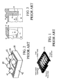
- A first variously developed solution is represented by a power device realised by means of a conveniently shaped metal container or frame suitable to draw at the same level in an upper surface the device conduction terminal (drain) located on a lower surface. An embodiment thereof is shown in figure 1 and described in the document MOSFET BGA design - Fairchild Semiconductor - August 2002. In this document, a method is described for realising a power device comprising an assembly step wherein the device integrated on the semiconductor (die) is welded inside a frame through conventional so-called die attach techniques.
- Although advantageous under several aspect the solution being provided has the drawback that the levelling of conduction terminals (source, gate) located on the device upper surface with the conduction terminal (drain) located on the opposite surface, and drawn on this surface, is ensured in the absence of the frame mechanical tolerances, of the semiconductor chip thickness as well as of the thickness of the welding compound used for the die attach technique. Therefore this solution is not sufficiently reliable for the realisation of large-scale-efficiency vertical conduction power devices.
- A second known solution, commonly indicated with the term WLCSP (Wafer Level Chip Scale Package), provides for the complete removal of the metal frame by realising a package immediately on a silicon chip, whereon a plurality of dies are integrated, before splitting the single dies. In the realisation of vertical conduction devices having overlapped dies, conduction terminals are drawn on a same device surface. This solution provides the realisation of deep sinkers, along the die outer perimeter, crossing the whole silicon chip thickness, which are filled with a conductive material such as a metal (for example gold).
- Also this second known solution, although advantageous under several aspects, has the drawback that the current flow, coming from the terminal located in the die lower surface, can be collected only along the outer perimeter of the device upper surface. This implies that the resistive contribution due to the current flow path on the substrate is considerable. Moreover the provided realisation method is very complex and thus rarely used.
- It is also known to realise a vertical conduction power device through the so-called Flip Chip BGA (Ball Grid Array) technique providing that "bumps", made of tin-based welding alloys, are positioned on the chip conduction pads, in order to allow the same to be directly connected on the board (fig. 2). This technique requires that a wettable metal is arranged on the pads.
- The Flip Chip BGA technique is used in the US patent application no. US 2001/0045635 by Kinzer wherein the device drain is surfaced by means of deep and heavily-doped sinkers or sinkers filled with a conductive layer (metal or polysilicon) creating conductive paths between the substrate and the metallisation on the device surface (fig. 3). Sinkers are located along the device perimeter and the current flow from the die centre towards the perimeter only relies on the conductive substrate made of heavily-doped silicon.
- This third known solution has however the drawback that sinkers are realised along the device perimeter and the substrate, mainly when big-sized, gives a considerable resistive contribution which, in case of application to low-voltage electronic power devices (20,50 Volt), has unacceptable values. Moreover in this known solution the contact area with the printed circuit board is reduced, being it limited to the bumps.
- The technical problem underlying the present invention is to provide a vertical conduction electronic power device having a reduced output resistance, a low thermal resistance, a reduced size and a reduced gate change value, this device having on a same surface all conduction terminals and having such structural and functional features as to allow the drawbacks mentioned with reference to the prior art to be overcome.
- The solution idea underlying the present invention is to realise all conduction terminals on a same device surface by means of a plurality of modules having an independent structure and a closed contour.
- Based on this solution idea the technical problem is solved by a vertical conduction electronic power device according to claim 1.
- The technical problem is also solved by a realisation method of a vertical conduction power device as previously indicated and described in the characterising part of
claim 10. - The features and advantages of the vertical conduction power device and method according to the invention will be apparent from the following description of embodiments thereof given by way of non limiting example with reference to the attached drawings.
-
- Figure 1, 2 and 3 schematically show embodiments of an electronic power device according to the prior art;
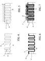
- Figures 4 to 7 schematically show in vertical section and enlarged scale a portion of a power device in the different steps of the realisation method according to the invention;
- figure 8 is a view from above of a power device realised according to the present invention;
- Figure 9 shows an enlarged detail of the device of figure 8;
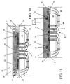
- Figures 10 and 11 schematically show sections according to the lines A-A' and B-B' of the device of figure 8;
- Figures 12 to 17 are views from above and sectional views respectively of different embodiments of sinker ducts according to the invention;
- Figures 18 and 19 show the values of some significant Q-features between devices realised according to the prior art and to the present invention as a table and graphically.
- With reference to the figures, and particularly to the example of figure 8, a vertical conduction electronic power device, particularly a MOS transistor, realised according to the present invention, is globally and schematically indicated with D.
- The present invention will be described hereafter with reference to the realisation of vertical conduction MOS power devices but it can be advantageously applied to the realisation of any vertical conduction power device such as for example BJT (Bipolar Junction Transistor), diodes, IGBT (Insulated Gate Bipolar Transistor) or power MOS both with planar structure and trench-gate.
- The process steps and structures described hereafter do not form a complete process flow for producing integrated circuits. In fact the present invention can be implemented together with the integrated circuit realisation techniques presently used in this field, and only those realisation steps being necessary to understand the invention will be described hereafter.
- Figures showing cross sections of portions of a device are not drawn to scale, but they are drawn to show the main features of the invention.
- The device D, shown in figure 8, is configured as a set of
modular areas 100 being approached to each other and extending parallel to each other. - More particularly, the device D comprises a plurality of rectangular
elongate source areas 25, each surrounded by anarrow gate area 20 and delimited by a closedgate contour 23, as better shown in figure 9. - These
source areas 25, and thusgate areas 20, extend parallel to each other and they are mutually separated by a first longitudinally-extendingregion 30a, withdrain area 30. - Moreover, as particularly emphasised in figure 8, the device D has all along an outer perimeter P, a second closed
region 30b, withdrain area 30, which substantially configures an outer edge. - With particular reference to figures 10 and 11, showing portions of the device D according to a section A-A' and a section B-B' respectively, the device D is realised on a
semiconductor material substrate 10, while thesource 25,gate 20 anddrain 30 areas are realised in anepitaxial layer 40 arranged on thesubstrate 10. - In the
epitaxial layer 40 in correspondence with thedrain areas 30, both below thefirst regions 30a and the second closedregion 30b, the device D comprises asinker structure 45, created by realising a quite dense grid of sinkers S. - Advantageously a portion of this
sinker structure 45 underlying two firstadjacent regions 30a and corresponding portions of secondperipheral regions 30b, is arranged perimetrically to eachmodular area 100 defining the device D. - Substantially, the device D is configured as a set of
modular areas 100 extending parallel to each other, each having a rectangularelongate source area 25 surrounded by anarrow gate area 20, delimited by aclosed contour 23, and separated from each other byregions 30a withdrain area 30 extending parallel and connected at the opposite ends thereof to a secondclosed region 30b withdrain area 30 forming a device outer peripheral edge; as well as asinker structure 45 extending perpendicularly to the substrate and formed by a grid of sinker S located below both the firstparallel regions 30a and the secondclosed region 30b withdrain area 30 in order to favour a conductive channel for a current coming from thesource area 25 and directed towards thedrain area 30 across thesubstrate 10. - Advantageously, as emphasised in figures 10 and 11, each sinker S is deeper than the thickness of the
epitaxial layer 40 and such as to penetrate at least partially thesubstrate 10. Each sinker S thus allows a conductive channel to be realised for the current in thesubstrate 10, coming from thesource area 25 and directed towards thedrain area 30 of eachmodular area 100. - As emphasised in figures 4 to 7, each sinker S has, near the walls, a
layer 47 of enriched material allowing the contact resistance of the sinker S to be improved, moreover ametal 49 such as for example a tungsten plug is deposited all along the useful depth as emphasised in figures 7, 12 and 13. - With reference to figures 10 and 11, respective gate metallisation or
metal strips 21, realised by sputtering, are provided on eachgate area 20 in order to allow the electrical connection thereof. - Similarly, further metallisation or
metal strips source 25 and drain 30 area respectively, in the latter case both on thefirst regions 30a and thesecond region 30b. - A
dielectric layer 50, arranged on the whole upper surface of the device D, has such a thickness as to completely cover metallisation strips 21, 26 and 31. - Conveniently, the
dielectric layer 50 has a plurality ofgate 22,source 27 and drain 32 vias contacts, the latter being visible only in figure 8, respectively obtained through openings realised by photolithography on the first metallisation ormetal level gate 20,source 25 and drain 30 areas, so as to allow an electric communication. - Particularly, in each rectangular elongate
modular area 100, source vias 27 occupy a substantially central portion, gate vias 22 occupy a portion arranged laterally and outside source vias 27 and drain vias 32 occupy the two transverse opposite ends of eachmodular area 100. - Advantageously, the device D has on the dielectric layer 50 a source terminal or electrode or
pad 65, a gate one 60 and a pair ofdrains modular area 100. - In particular, according to a preferred embodiment, each pad of the pair of
drain pads source 65 andgate 60 pads are arranged inside the pair ofdrain pads - Conveniently, the
source 65,gate 60 pads and the pair ofdrains dielectric layer 50 of the device D. The second metallisation being obtained by sputtering by using some wettable material from the traditional welding compounds used in electronics. - Obviously the
source 65,gate 60 pads and the pair ofdrain pads gate 22,source 27 and drain 32 vias, on a second metallisation level, allowing the electric connection. - In particular, the pair of
drain pads drain vias 32, allows the current in thesubstrate 10 coming from thesource area 25 and directed towards thedrain area 30 for eachmodular area 100 to be surfaced. The current is thus caught not only by thesinker structure 45 on the outer perimeter P of the device D below thesecond region 30b but also by thesinker structure 45 in eachfirst region 30a interposed between amodular area 100 and the other on the whole longitudinal length of the device D. - The presence of the
sinker structure 45 thus allows the functionality and efficiency of the device D to be considerably improved minimising the resistive contribution due to the reduced path performed by the current because of thesinker structure 45 itself in eachmodular area 100. - Moreover, the presence of the
sinker structure 45 and of the drain vias 32 in correspondence with the outer perimeter P allows an excellent operation of the device D to be ensured during the interdiction step. - In order to complete the so-obtained device D, the
semiconductor substrate 10 can be conveniently reduced and the device D can have a metal bottom, not shown in the figures being it conventional. - It is worth noting that figure 8 shows the
source 27 and drain 32 vias, but notgate vias 22 only for figure resolution issues. Moreover, the device D is shown by considering the surfacetransparent dielectric layer 50, in order to show the details of underlying layers. - The invention also relates to a realisation method of a vertical conduction electronic power device and it is shown hereafter with reference to figures 4 to 11.
- The realised power device is the one represented in figure 8 and the same numeral references will be used hereafter to indicate corresponding parts.
- The realisation method according to the invention provides the following steps:
- Growing an
epitaxial layer 40 on asemiconductor substrate 10; - Realising
respective gate 20,source 25 and drain 30 areas in thatepitaxial layer 40. - Advantageously according to the invention, the realisation steps of the
drain 30,gate 20 andsource 25 areas comply with a layout shown in figure 8 according to which the device D is configured as a set ofmodular areas 100 being approached to each other and extending parallelly. More particularly, the device D comprises a plurality ofrectangular source areas 25, each surrounded by anarrow gate area 20, delimited by agate contour 23, and each separated from one another by a first longitudinally-extendingregion 30a, withdrain area 30. Moreover the device D has all along an outer perimeter P, a secondclosed region 30b, withdrain area 30. - The method further provides the steps of:
- Depositing a thin layer of dielectric material, for example a 0,5um-thick oxide, on the
epitaxial layer 40, not shown in the figures, and eventually performing a dielectric thickening thermal process; - Opening the contacts in correspondence with the body, gate and source areas;
- Realising through photolithography, in correspondence with the
drain area 30, and also in correspondence with thefirst regions 30a and thesecond region 30b, asinker structure 45 realising a quite dense grid of sinkers S being parallel to each other and structurally independent. - Advantageously, the photolithographic step realises each sinker S of the
sinker structure 45 with a higher depth than the thickness of theepitaxial layer 40 and such as to penetrate at least partially thesubstrate 10. In a preferred embodiment, each sinker S is deeper than (3-10) um and the width thereof ranges between 0,6 and 1um. - The realisation method according to the invention also provides the steps of:
- Performing, as shown in figures 4 to 7, an enrichment implant on the
sinker structure 45 allowing the contact resistance to be improved. Preferably the enrichment implant occurs according to the following features 1E15P/cm2 at 30 KeV and it is performed with a tilt angle varying from +7° to -7° to allow both side walls of each sinker S to be implanted for the whole depth improving the implant efficiency; - Eventually performing an annealing process;
- Depositing a first steel barrier, not emphasised in the figures, for example by means of an alloy Ti/TiN, and eventually performing a silicidation, as for exemple the realisated device subjectes per 30 sec. At 80° C;
- Filling all the previously opened contacts and the sinkers S of the
sinker structure 45 for the whole depth thereof with aconductive material 49, particularly a metal one, such as for example a 0,3-0,7 um-thick tungsten plug (W-plug); - Performing an etch back step of the
conductive material 49; - Depositing a second steel barrier layer preferably by means for example of 0,1 um of Ti, not shown in the figures;
- Realising by sputtering a first metallisation, preferably by using AlSiCu with a thickness from 0,5um to 3um; and
- Realising through photolithography on the first metallisation and on the steel barrier layer
convenient gate 21,source 26 and drain 31 metallisations in eachmodular area 100 which, overlappingrespective gate 20,source 25 and drain 30 areas, define convenient closed contour structures. - Performing an alloy thermal process;
- Depositing a
dielectric layer 50 with such a thickness as to completelyoverhang gate 20,source 25 and drain 30 metallisations, for example by using 1um of oxide; - Realising through a photolithographic step on the dielectric layer 50 a plurality of contact vias for the
source 27,gate 22 and drain 32 regions to open connection vias with thegate 20,source 25 and drain 30 metallisations. -
Advantageously source 27,gate 22 and drain 32 vias will occupy transverse areas of eachmodular area 100. In particular,source 27 vias will occupy a substantially central area of eachmodular area 100,gate 22 vias will occupy a portion arranged laterally to sourcevias 27 and drain vias 32 will occupy the two transverse ends of eachmodular area 100. - The realisation method thus provides to continue with the following steps of:
- Performing a second metallisation by sputtering, using a material being conveniently wettable by traditional welding compounds, preferably Ti/Ni/Au or Ti/NiAg;
- Performing a photolithographic step of the second metallisation defining on the
source 27,gate 22 and drain 32vias corresponding source 65,gate 60 electrodes or pads and a pair ofdrain electrodes modular area 100; - Traditionally completing the device D by eventually realising a reduction of the
semiconductor substrate 10 and eventually inserting a metal bottom. - The realisation method according to the invention allows a vertical conduction power device D to be realised having the three conduction terminals brought on the same device surface, arrangement being obtained by means of a synergy between the device layout and a process sequence.
- It is also possible to envisage alternative embodiments of the vertical conduction power device according to the invention. As shown in figures 14 and 15 a first alternative embodiment emphasises a possible solution for a second embodiment of the
sinker structure 45. - Preferably in this solution the
sinker structure 45 has a plurality ofconnection ducts 95 between sinkers S being plan parallely arranged, allowing the flowing current distribution, coming from the source area and directed towards the drain area. The plurality ofducts 95 can be realised by means of a convenient mask during the photolithographic step. - A further embodiment of the vertical conduction power device D provides, in correspondence with the drain area, a
single trench 96, realised as an alternative to single sinkers S of thesinker structure 45, as indicated in figures 16 and 17. - The
trench 96 occupies the whole available area and it is filled by thehigh conductivity material 49 as indicated in figure 17 allowing the current to flow from the source to the drain. - The main advantage of the vertical conduction power device realised according to the present invention is to bring on a same surface the source, gate electrodes and the drain electrode by means of a particular device layout arrangement.
- A further advantage of the device realised according to the present invention is to obtain with the particular layout arrangement a plurality of juxtaposed structurally-independent modules, each one having a source, gate metallisation and a drain metallisation realised in correspondence with the closed contour.
- The presence of the sinker structure is also advantageous, which, realised in correspondence with the drain area, is arranged on the perimeter of each modular area and on the device outer edge, thus ensuring an excellent device operation in the interdiction step.
- A further advantage of the device realised according to the present invention is that the sinker structure created by realising a quite dense grid of sinkers without excessively penalising the active area minimises the resistive contribution due to the current path on the substrate and it thus reduces the device output resistance.
- Another advantage of the so-realised device is that the reduced size of each sinker facilitates and simplifies the filling thereof with a high conductivity metal layer.
- The size of contact terminals is also advantageous for the device realised according to the present invention, in fact they have a contact area with the board being much larger than the size of previous devices and this generates significant advantages on the resistive contribution.
- From experimental tests carried out by the Applicant it was possible to verify that the so-obtained device, although the presence of the sinker structure limits the possibility to exploit the whole semiconductor layer, has a gain on the resistive contributions of the drain terminal resulting in an advantage of the device in the dynamic operation thereof, as it can be seen in the table of figure 18.
- Always from experimental tests carried out by the Applicant it is possible to verify that the device realised according to the invention has an extremely reduced product between the output resistance, the Gate change and the Footprint, as it can be seen from the comparison diagram in figure 19.
- Last but not least, the device realised according to the present invention has a simple, efficient and reduced-cost process sequence.
Claims (18)
- A vertical conduction electronic power device being integrated ona semiconductor substrate (10), comprising respective gate (20), source (25) and drain (30) areas, realised in an epitaxial layer (40) arranged on said semiconductor substrate (10) and comprising respective gate (21), source (26) and drain (31) metallisations realised by means of a first metallisation level as well as gate (60), source (65) and drain (70) terminals or pads realised by means of a second metallisation level, characterised in that it is configured as a set of modular areas (100) extending parallel to each other, each having a rectangular elongate source area (25) perimetrically surrounded by a narrow gate area (20), and separated from each other by regions (30a) with drain area (30) extending parallel and connected at the opposite ends thereof to a second closed region (30b) with drain area (30) forming a device outer peripheral edge; as well as a sinker structure (45) extending perpendicularly to the substrate and formed by a grid of sinker (S) located below both the first parallel regions (30a) and the second closed region (30b) with drain area (30) in order to favour a conductive channel for a current coming from the source area (25) and directed towards the drain area (30) across the substrate (10).
- A device according to claim 1, characterised in that in adjacent modular areas (100) said drain area (30) and said source area (25) are separated by said gate area (20).
- A device according to claim 1 and 2, characterised in that each modular area (100) is perimetrically delimited on the long sides by two parallel regions (30a) with drain area (30) and on the short sides by two sections of the region (30b) with drain area corresponding to sections of the device outer edge (29).
- A device according to claim 1, characterised in that each gate area (20) of each modular area (100) is delimited by a closed gate contour (23).
- A device according to claim 1 and 3, characterised in that said sinker structure (31) is extended with a higher depth than the thickness of said epitaxial layer (40) penetrating at least partially in said substrate (10).
- A device according to claim 1, characterised in that each of said sinkers (S) has, near the peripheral walls, an enriched material layer (32) for the whole useful depth.
- A device according to claims 1 to 6, characterised in that said gate (21), source (26) and drain (31) metallisations realised on said gate (20), source (25) and drain (30) areas in each module (100) by means of said first metallisation level have a closed contour.
- A device according to claims 1 to 7, characterised in that it has on said gate (21), source (26) and drain (31) metallisations a second dielectric material layer (50) wherethrough multiple source (27), gate (22) and drain (32) contact vias are realised, said source vias (27) occupying a substantially central portion, said gate vias (22) occupying a portion arranged laterally and outside said source vias (27) and said drain vias (32) partially occupying said closed contour (33).
- A device according to claims 1 to 8, characterised in that said source (65), gate (60) and drain (70a e 70b) terminals, realised by means of said second metallisation, are arranged on a same surface.
- A realisation method of a vertical conduction electronic power device provides the following steps:- Growing an epitaxial layer (40) on a semiconductor substrate (10);- Realising respective source (25), gate (20), and drain (30) areas in said epitaxial layer (40);Characterised in that said source areas (25) are realised with a rectangular elongate shape and perimetrically surrounded by a narrow gate area (20) to form modular areas (100) separated from each other by regions (30a) with drain area (30) extending parallel and connected at the opposite ends thereof to a second closed region (30b) with drain area (30) forming a device outer peripheral edge and in that a sinker structure (31) is formed in advance under said drain areas.
- A device realisation method according to claim 10, characterised in that it further provides the following steps of:- Depositing a thin layer of dielectric material on said epitaxial layer (40) with following possible thickening thermal process of said dielectric;- Opening the contacts in correspondence with said gate and source areas;- Realising through photolithography, a sinker structure (31) with a dense grid of sinkers (S), below said drain area (30), each of said sinker (S) having a higher depth than the thickness of said epitaxial layer (40) and such as to penetrate at least partially said substrate (10) .
- A device realisation method according to claim 11, characterised in that it further provides the following steps of:- Performing an enrichment implant on the side walls of said sinker structure (31)- Eventually performing an annealing process;- Depositing a first steel barrier on said side walls, for example by means of an alloy Ti/TiN, and performing a silicidation step;- Filling the sinkers (S) of said sinker structure (31) for the whole depth thereof with a conductive metal material (34), for example a tungsten plug (W-plug);
- A device realisation method according to claim 12, characterised in that it further provides the following steps of:- Performing an etch back step of said conductive material (34);- Depositing a second steel barrier layer;- Realising by sputtering a first metallisation, preferably by using AlSiCu;- Realising through photolithography on said first metallisation and on said steel barrier layer a gate (21), source (26) and drain (31) metallisations in each module (100) overlapping said respective gate (20), source (25) and drain (30) areas, defining closed contour structures.
- A device realisation method according to claim 13, characterised in that it further provides the following steps of:- Performing an alloy thermal process;- Depositing a second dielectric material layer (50) with such a thickness as to completely overhang said gate (21), source (26) and drain (31) metallisations;- Realising through a photolithographic step a plurality of source (27), gate (22) and drain (32) vias allowing connection vias to be opened with said first metallisation, said source (27), gate (22) and drain (32) vias realised on each of said module (100) in correspondence with said source (26), gate (21) and drain (31) metallisations occupying transverse areas of said module (100), said source vias (27) occupying a substantially central area of said module (100), said gate vias (22) occupying an area arranged laterally to said source vias (27) and said drain vias (32) occupying the two ends on the closed contour.
- A device realisation method according to claim 11, characterised in that it further provides the following steps of:- Performing a second metallisation by sputtering, using a material being conveniently wettable by welding compounds;- Performing a photolithographic step of said second metallisation defining on said source (27), gate (22) and drain (32) vias corresponding source (65), gate (60) and drain (70a and 70b) electrodes, arranged transversely to each of said module (100).
- A device realisation method according to claim 10, characterised in that it provides the realisation of a plurality of connection ducts (95) between parallel sinkers (S), said plurality of ducts (95) being realised by means of a convenient mask during said photolithographic step.
- A device realisation method according to claim 11, characterised in that it has a single trench (96) realised in correspondence with said drain area (30), said trench (96) being filled with a high conductivity material (49).
- A device realisation method according to claim 12, characterised in that said enrichment implant occurs with features 1E15P/cm2 at 30KeV and which is performed with a tilt angle varying from +7° to -7°.
Priority Applications (5)
| Application Number | Priority Date | Filing Date | Title |
|---|---|---|---|
| EP10015764A EP2309545A3 (en) | 2004-09-30 | 2004-09-30 | Vertical power semiconductor device and method of making the same |
| EP04425733A EP1643558B1 (en) | 2004-09-30 | 2004-09-30 | Vertical power semiconductor device and method of making the same |
| US11/235,495 US8624332B2 (en) | 2004-09-30 | 2005-09-26 | Vertical conduction power electronic device and corresponding realization method |
| JP2005280012A JP2006108663A (en) | 2004-09-30 | 2005-09-27 | Vertically conductive power electronic device and method for realizing the same |
| US14/042,041 US8895370B2 (en) | 2004-09-30 | 2013-09-30 | Vertical conduction power electronic device and corresponding realization method |
Applications Claiming Priority (1)
| Application Number | Priority Date | Filing Date | Title |
|---|---|---|---|
| EP04425733A EP1643558B1 (en) | 2004-09-30 | 2004-09-30 | Vertical power semiconductor device and method of making the same |
Related Child Applications (1)
| Application Number | Title | Priority Date | Filing Date |
|---|---|---|---|
| EP10015764.3 Division-Into | 2010-12-17 |
Publications (2)
| Publication Number | Publication Date |
|---|---|
| EP1643558A1 true EP1643558A1 (en) | 2006-04-05 |
| EP1643558B1 EP1643558B1 (en) | 2012-05-02 |
Family
ID=34932796
Family Applications (2)
| Application Number | Title | Priority Date | Filing Date |
|---|---|---|---|
| EP10015764A Withdrawn EP2309545A3 (en) | 2004-09-30 | 2004-09-30 | Vertical power semiconductor device and method of making the same |
| EP04425733A Expired - Lifetime EP1643558B1 (en) | 2004-09-30 | 2004-09-30 | Vertical power semiconductor device and method of making the same |
Family Applications Before (1)
| Application Number | Title | Priority Date | Filing Date |
|---|---|---|---|
| EP10015764A Withdrawn EP2309545A3 (en) | 2004-09-30 | 2004-09-30 | Vertical power semiconductor device and method of making the same |
Country Status (3)
| Country | Link |
|---|---|
| US (2) | US8624332B2 (en) |
| EP (2) | EP2309545A3 (en) |
| JP (1) | JP2006108663A (en) |
Cited By (3)
| Publication number | Priority date | Publication date | Assignee | Title |
|---|---|---|---|---|
| EP1916716A3 (en) * | 2006-10-27 | 2009-08-19 | Sanyo Electric Co., Ltd. | Semiconductor device |
| EP3024035A4 (en) * | 2013-07-16 | 2016-08-31 | Panasonic Ip Man Co Ltd | SEMICONDUCTOR DEVICE |
| CN110673009A (en) * | 2019-10-14 | 2020-01-10 | 北京工业大学 | Grid leakage short circuit and grid voltage supply device for measuring SiC MOS thermal resistance under high voltage |
Families Citing this family (4)
| Publication number | Priority date | Publication date | Assignee | Title |
|---|---|---|---|---|
| US8717093B2 (en) * | 2010-01-08 | 2014-05-06 | Mindspeed Technologies, Inc. | System on chip power management through package configuration |
| US9997443B2 (en) * | 2013-02-25 | 2018-06-12 | Infineon Technologies Ag | Through vias and methods of formation thereof |
| US9159652B2 (en) | 2013-02-25 | 2015-10-13 | Stmicroelectronics S.R.L. | Electronic device comprising at least a chip enclosed in a package and a corresponding assembly process |
| CN110520999B (en) * | 2016-06-30 | 2023-09-29 | 德州仪器公司 | Chip-scale packaged power MOSFETs with metal-filled deep-sink contacts |
Citations (5)
| Publication number | Priority date | Publication date | Assignee | Title |
|---|---|---|---|---|
| US5242841A (en) | 1992-03-25 | 1993-09-07 | Texas Instruments Incorporated | Method of making LDMOS transistor with self-aligned source/backgate and photo-aligned gate |
| JPH06151863A (en) | 1992-11-05 | 1994-05-31 | Oki Electric Ind Co Ltd | Semiconductor device |
| US20010045635A1 (en) | 2000-02-10 | 2001-11-29 | International Rectifier Corp. | Vertical conduction flip-chip device with bump contacts on single surface |
| JP2002270814A (en) | 2001-03-12 | 2002-09-20 | Sanyo Electric Co Ltd | Semiconductor device and method of manufacturing the same |
| JP2002353452A (en) | 2001-05-25 | 2002-12-06 | Toshiba Corp | Power semiconductor device |
Family Cites Families (6)
| Publication number | Priority date | Publication date | Assignee | Title |
|---|---|---|---|---|
| JPH0619127B2 (en) | 1988-09-07 | 1994-03-16 | 西武ポリマ化成株式会社 | Impermeable structure and impermeable sheet for landfill |
| JP2899318B2 (en) | 1989-07-20 | 1999-06-02 | 東芝電池株式会社 | Alkaline storage battery |
| GB2373634B (en) * | 2000-10-31 | 2004-12-08 | Fuji Electric Co Ltd | Semiconductor device |
| US7195965B2 (en) * | 2002-10-25 | 2007-03-27 | Texas Instruments Incorporated | Premature breakdown in submicron device geometries |
| US7126193B2 (en) * | 2003-09-29 | 2006-10-24 | Ciclon Semiconductor Device Corp. | Metal-oxide-semiconductor device with enhanced source electrode |
| US7205629B2 (en) * | 2004-06-03 | 2007-04-17 | Widebandgap Llc | Lateral super junction field effect transistor |
-
2004
- 2004-09-30 EP EP10015764A patent/EP2309545A3/en not_active Withdrawn
- 2004-09-30 EP EP04425733A patent/EP1643558B1/en not_active Expired - Lifetime
-
2005
- 2005-09-26 US US11/235,495 patent/US8624332B2/en not_active Expired - Fee Related
- 2005-09-27 JP JP2005280012A patent/JP2006108663A/en not_active Withdrawn
-
2013
- 2013-09-30 US US14/042,041 patent/US8895370B2/en not_active Expired - Fee Related
Patent Citations (5)
| Publication number | Priority date | Publication date | Assignee | Title |
|---|---|---|---|---|
| US5242841A (en) | 1992-03-25 | 1993-09-07 | Texas Instruments Incorporated | Method of making LDMOS transistor with self-aligned source/backgate and photo-aligned gate |
| JPH06151863A (en) | 1992-11-05 | 1994-05-31 | Oki Electric Ind Co Ltd | Semiconductor device |
| US20010045635A1 (en) | 2000-02-10 | 2001-11-29 | International Rectifier Corp. | Vertical conduction flip-chip device with bump contacts on single surface |
| JP2002270814A (en) | 2001-03-12 | 2002-09-20 | Sanyo Electric Co Ltd | Semiconductor device and method of manufacturing the same |
| JP2002353452A (en) | 2001-05-25 | 2002-12-06 | Toshiba Corp | Power semiconductor device |
Non-Patent Citations (3)
| Title |
|---|
| PATENT ABSTRACTS OF JAPAN vol. 018, no. 464 (E - 1598) 29 August 1994 (1994-08-29) * |
| PATENT ABSTRACTS OF JAPAN vol. 2003, no. 01 14 January 2003 (2003-01-14) * |
| PATENT ABSTRACTS OF JAPAN vol. 2003, no. 04 2 April 2003 (2003-04-02) * |
Cited By (4)
| Publication number | Priority date | Publication date | Assignee | Title |
|---|---|---|---|---|
| EP1916716A3 (en) * | 2006-10-27 | 2009-08-19 | Sanyo Electric Co., Ltd. | Semiconductor device |
| US7915740B2 (en) | 2006-10-27 | 2011-03-29 | Sanyo Electric Co., Ltd. | Semiconductor device |
| EP3024035A4 (en) * | 2013-07-16 | 2016-08-31 | Panasonic Ip Man Co Ltd | SEMICONDUCTOR DEVICE |
| CN110673009A (en) * | 2019-10-14 | 2020-01-10 | 北京工业大学 | Grid leakage short circuit and grid voltage supply device for measuring SiC MOS thermal resistance under high voltage |
Also Published As
| Publication number | Publication date |
|---|---|
| JP2006108663A (en) | 2006-04-20 |
| US20140045309A1 (en) | 2014-02-13 |
| US8624332B2 (en) | 2014-01-07 |
| US20060071242A1 (en) | 2006-04-06 |
| EP2309545A3 (en) | 2011-10-12 |
| US8895370B2 (en) | 2014-11-25 |
| EP2309545A2 (en) | 2011-04-13 |
| EP1643558B1 (en) | 2012-05-02 |
Similar Documents
| Publication | Publication Date | Title |
|---|---|---|
| US8895370B2 (en) | Vertical conduction power electronic device and corresponding realization method | |
| US9520468B2 (en) | Integrated power device on a semiconductor substrate having an improved trench gate structure | |
| US9647078B2 (en) | Closed cell configuration to increase channel density for sub-micron planar semiconductor power device | |
| US8357973B2 (en) | Inverted-trench grounded-source FET structure with trenched source body short electrode | |
| US7560808B2 (en) | Chip scale power LDMOS device | |
| TWI482281B (en) | Semiconductor device and method of manufacturing same | |
| US7936011B2 (en) | Shielded gate trench (SGT) MOSFET devices and manufacturing processes | |
| JPH11243196A (en) | Field effect transistor and method of manufacturing the same | |
| JP2008166775A (en) | Semiconductor device and manufacturing method thereof | |
| US5888889A (en) | Integrated structure pad assembly for lead bonding | |
| US5070388A (en) | Trench-resident interconnect structure | |
| CN207781613U (en) | Power semiconductor | |
| US8420525B2 (en) | Semiconductor device with vertical current flow and low substrate resistance and manufacturing process thereof | |
| TW200824086A (en) | Power supply network | |
| CN207781615U (en) | Power semiconductor | |
| CN207781610U (en) | Power semiconductor | |
| US20200365708A1 (en) | Power semiconductor devices having reflowed inter-metal dielectric layers | |
| CN114496987B (en) | MOSFET power device, forming method thereof and CSP packaging module | |
| US20240203835A1 (en) | Semiconductor device | |
| CN120711823A (en) | A power discrete device with integrated resistor and its manufacturing method | |
| WO2025221481A1 (en) | Jfet device with improved area utilization | |
| CN119767725A (en) | GaN-based HEMT device structure and manufacturing method thereof | |
| CN102832244A (en) | Semiconductor device with device terminal electrode exposed at substrate end and method for manufacturing same | |
| JPH07142709A (en) | Vertical MOSFET | |
| HK1112112A1 (en) | Semiconductor power device having a top-side drain using a sinker trench |
Legal Events
| Date | Code | Title | Description |
|---|---|---|---|
| PUAI | Public reference made under article 153(3) epc to a published international application that has entered the european phase |
Free format text: ORIGINAL CODE: 0009012 |
|
| AK | Designated contracting states |
Kind code of ref document: A1 Designated state(s): AT BE BG CH CY CZ DE DK EE ES FI FR GB GR HU IE IT LI LU MC NL PL PT RO SE SI SK TR |
|
| AX | Request for extension of the european patent |
Extension state: AL HR LT LV MK |
|
| 17P | Request for examination filed |
Effective date: 20061004 |
|
| AKX | Designation fees paid |
Designated state(s): DE FR GB IT |
|
| 17Q | First examination report despatched |
Effective date: 20081216 |
|
| R17C | First examination report despatched (corrected) |
Effective date: 20081217 |
|
| RAP1 | Party data changed (applicant data changed or rights of an application transferred) |
Owner name: STMICROELECTRONICS SRL |
|
| RIC1 | Information provided on ipc code assigned before grant |
Ipc: H01L 29/739 20060101ALI20110927BHEP Ipc: H01L 21/329 20060101ALI20110927BHEP Ipc: H01L 29/08 20060101ALN20110927BHEP Ipc: H01L 29/417 20060101ALI20110927BHEP Ipc: H01L 29/78 20060101AFI20110927BHEP Ipc: H01L 21/331 20060101ALI20110927BHEP Ipc: H01L 21/336 20060101ALI20110927BHEP Ipc: H01L 29/732 20060101ALI20110927BHEP Ipc: H01L 29/861 20060101ALI20110927BHEP Ipc: H01L 29/06 20060101ALI20110927BHEP Ipc: H01L 21/265 20060101ALN20110927BHEP |
|
| GRAP | Despatch of communication of intention to grant a patent |
Free format text: ORIGINAL CODE: EPIDOSNIGR1 |
|
| GRAS | Grant fee paid |
Free format text: ORIGINAL CODE: EPIDOSNIGR3 |
|
| GRAA | (expected) grant |
Free format text: ORIGINAL CODE: 0009210 |
|
| RAP1 | Party data changed (applicant data changed or rights of an application transferred) |
Owner name: STMICROELECTRONICS S.R.L. |
|
| AK | Designated contracting states |
Kind code of ref document: B1 Designated state(s): DE FR GB IT |
|
| REG | Reference to a national code |
Ref country code: GB Ref legal event code: FG4D |
|
| RAP2 | Party data changed (patent owner data changed or rights of a patent transferred) |
Owner name: STMICROELECTRONICS SRL |
|
| REG | Reference to a national code |
Ref country code: DE Ref legal event code: R096 Ref document number: 602004037593 Country of ref document: DE Effective date: 20120705 |
|
| PG25 | Lapsed in a contracting state [announced via postgrant information from national office to epo] |
Ref country code: IT Free format text: LAPSE BECAUSE OF FAILURE TO SUBMIT A TRANSLATION OF THE DESCRIPTION OR TO PAY THE FEE WITHIN THE PRESCRIBED TIME-LIMIT Effective date: 20120502 |
|
| PLBE | No opposition filed within time limit |
Free format text: ORIGINAL CODE: 0009261 |
|
| STAA | Information on the status of an ep patent application or granted ep patent |
Free format text: STATUS: NO OPPOSITION FILED WITHIN TIME LIMIT |
|
| 26N | No opposition filed |
Effective date: 20130205 |
|
| GBPC | Gb: european patent ceased through non-payment of renewal fee |
Effective date: 20120930 |
|
| REG | Reference to a national code |
Ref country code: DE Ref legal event code: R097 Ref document number: 602004037593 Country of ref document: DE Effective date: 20130205 |
|
| PG25 | Lapsed in a contracting state [announced via postgrant information from national office to epo] |
Ref country code: GB Free format text: LAPSE BECAUSE OF NON-PAYMENT OF DUE FEES Effective date: 20120930 |
|
| PGFP | Annual fee paid to national office [announced via postgrant information from national office to epo] |
Ref country code: FR Payment date: 20130920 Year of fee payment: 10 |
|
| REG | Reference to a national code |
Ref country code: FR Ref legal event code: ST Effective date: 20150529 |
|
| PG25 | Lapsed in a contracting state [announced via postgrant information from national office to epo] |
Ref country code: FR Free format text: LAPSE BECAUSE OF NON-PAYMENT OF DUE FEES Effective date: 20140930 |
|
| REG | Reference to a national code |
Ref country code: DE Ref legal event code: R082 Ref document number: 602004037593 Country of ref document: DE Representative=s name: SCHMITT-NILSON SCHRAUD WAIBEL WOHLFROM PATENTA, DE |
|
| PGFP | Annual fee paid to national office [announced via postgrant information from national office to epo] |
Ref country code: DE Payment date: 20200819 Year of fee payment: 17 |
|
| REG | Reference to a national code |
Ref country code: DE Ref legal event code: R119 Ref document number: 602004037593 Country of ref document: DE |
|
| PG25 | Lapsed in a contracting state [announced via postgrant information from national office to epo] |
Ref country code: DE Free format text: LAPSE BECAUSE OF NON-PAYMENT OF DUE FEES Effective date: 20220401 |