EP1641055A1 - Method for fabricating organic electroluminescence device - Google Patents
Method for fabricating organic electroluminescence device Download PDFInfo
- Publication number
- EP1641055A1 EP1641055A1 EP05108609A EP05108609A EP1641055A1 EP 1641055 A1 EP1641055 A1 EP 1641055A1 EP 05108609 A EP05108609 A EP 05108609A EP 05108609 A EP05108609 A EP 05108609A EP 1641055 A1 EP1641055 A1 EP 1641055A1
- Authority
- EP
- European Patent Office
- Prior art keywords
- electroluminescence device
- laser beam
- organic electroluminescence
- substrate
- organic
- Prior art date
- Legal status (The legal status is an assumption and is not a legal conclusion. Google has not performed a legal analysis and makes no representation as to the accuracy of the status listed.)
- Ceased
Links
Images

Classifications
-
- H—ELECTRICITY
- H05—ELECTRIC TECHNIQUES NOT OTHERWISE PROVIDED FOR
- H05B—ELECTRIC HEATING; ELECTRIC LIGHT SOURCES NOT OTHERWISE PROVIDED FOR; CIRCUIT ARRANGEMENTS FOR ELECTRIC LIGHT SOURCES, IN GENERAL
- H05B33/00—Electroluminescent light sources
- H05B33/10—Apparatus or processes specially adapted to the manufacture of electroluminescent light sources
-
- B—PERFORMING OPERATIONS; TRANSPORTING
- B23—MACHINE TOOLS; METAL-WORKING NOT OTHERWISE PROVIDED FOR
- B23K—SOLDERING OR UNSOLDERING; WELDING; CLADDING OR PLATING BY SOLDERING OR WELDING; CUTTING BY APPLYING HEAT LOCALLY, e.g. FLAME CUTTING; WORKING BY LASER BEAM
- B23K26/00—Working by laser beam, e.g. welding, cutting or boring
- B23K26/02—Positioning or observing the workpiece, e.g. with respect to the point of impact; Aligning, aiming or focusing the laser beam
- B23K26/06—Shaping the laser beam, e.g. by masks or multi-focusing
- B23K26/064—Shaping the laser beam, e.g. by masks or multi-focusing by means of optical elements, e.g. lenses, mirrors or prisms
- B23K26/066—Shaping the laser beam, e.g. by masks or multi-focusing by means of optical elements, e.g. lenses, mirrors or prisms by using masks
-
- H—ELECTRICITY
- H10—SEMICONDUCTOR DEVICES; ELECTRIC SOLID-STATE DEVICES NOT OTHERWISE PROVIDED FOR
- H10K—ORGANIC ELECTRIC SOLID-STATE DEVICES
- H10K50/00—Organic light-emitting devices
- H10K50/10—OLEDs or polymer light-emitting diodes [PLED]
- H10K50/11—OLEDs or polymer light-emitting diodes [PLED] characterised by the electroluminescent [EL] layers
-
- H—ELECTRICITY
- H10—SEMICONDUCTOR DEVICES; ELECTRIC SOLID-STATE DEVICES NOT OTHERWISE PROVIDED FOR
- H10K—ORGANIC ELECTRIC SOLID-STATE DEVICES
- H10K71/00—Manufacture or treatment specially adapted for the organic devices covered by this subclass
- H10K71/10—Deposition of organic active material
- H10K71/18—Deposition of organic active material using non-liquid printing techniques, e.g. thermal transfer printing from a donor sheet
Definitions
- the present invention relates to a method for fabricating an organic electroluminescence device, more particularly, to a method for forming the organic film layer pattern using a laser irradiation apparatus equipped with a diffractive optical element when forming an organic layer pattern by laser induced thermal imaging (LITI).
- LITI laser induced thermal imaging
- the organic layers comprise at least an emitting layer and further comprise a hole injection layer, a hole transport layer, an electron transport layer and an electron injection layer in addition to the emitting layer.
- the organic electroluminescence device is classified into a high molecular organic electroluminescence device and a small molecular organic electroluminescence device according to materials composing the organic layers, particularly the emitting layer.
- the emitting layer should be patterned to realize full coloration of the organic electroluminescence device, wherein a method for patterning the emitting layer includes a photolithography process using a shadow mask in case of the small molecular organic electroluminescence device, and an ink-jet printing method or a laser induced thermal imaging (hereinafter referred to as "LITI") method using laser in case of the high molecular organic electroluminescence device.
- LITI laser induced thermal imaging
- a method for forming patterns of the organic layers by the LITI method requires at least a laser generator, an organic electroluminescence device substrate and a donor substrate.
- a method of patterning organic layers on the substrate comprises a step of absorbing a laser beam coming out of the laser generator into a light-to-heat conversion layer of the donor substrate such that the laser beam is converted into thermal energy, and a step of transferring a material composing a transfer layer onto the substrate by the thermal energy.
- the method of patterning organic layers on the substrate is disclosed in Korean Patent Application No. 1998-51844 and United States Patent Nos. 5,998,085, 6,214,520 and 6,114,088.
- FIG. 1 is a schematic drawing for explaining a method for fabricating an organic electroluminescence device according to the prior art.
- a substrate 110 on which a pixel electrode is formed is provided. Subsequently, a donor substrate 120 on which an organic layer 130 is formed is laminated on the pixel electrode formed substrate 110.
- An organic layer pattern is formed on the pixel electrode formed substrate 110 by irradiating a laser beam 150 onto the donor substrate 120 using a laser irradiation apparatus 100.
- the laser irradiation apparatus 100 comprises a laser generator 140, a patterned mask 160 and a projection lens 170.
- An organic layer pattern is formed on the substrate 110 by forming a laser beam 150 generated by the laser generator 140 as a pattern having a desired shape through the patterned mask 160 formed on a lower part of the laser generator 140 such that the laser beam 150 is irradiated onto the donor substrate 110.
- All laser beams 150 generated from the laser generator 140 do not pass through the patterned mask 160. That is, although a laser beam irradiated on a patterned part of the mask 160 is irradiated onto the projection lens 170 through the mask 160, a laser beam irradiated on a non-patterned part of the mask 160 is cut off by the mask 160. Therefore, a large amount of laser beam including the laser beam cut off by the mask 160 is required to form the organic layer pattern. After all, there is a problem that efficiency of laser beam is deteriorated.
- an object of the present invention to provide a method for fabricating an organic electroluminescence device, that is capable of improving energy efficiency of laser beam by using a diffractive optical element when forming an organic layer pattern by LITI and that is capable of reducing cost by forming an organic layer pattern having various shapes in the state that only a mask is replaced.
- the present invention provides a method for fabricating an organic electroluminescence device comprising a step of providing a substrate on which a pixel electrode is formed, a step of laminating a donor substrate on the front of the substrate, and a step of forming an organic layer pattern on the substrate by irradiating a laser beam onto a predetermined region of the donor substrate using a laser irradiation apparatus equipped with a diffractive optical element.
- the laser irradiation apparatus comprises a laser generator, a diffractive optical element formed under the laser generator to diffract a laser beam generated from the laser generator, a patterned mask formed under the diffractive optical element, and a projection lens formed under the patterned mask.
- the step of forming the organic layer pattern on the pixel electrode is performed at an atmoshphere of nitrogen gas (N 2 ) or in a vacuum environment.
- the organic layer pattern is a single layer or multilayer selected from the group consisting of an emitting layer, a hole injection layer, a hole transport layer, an electron transport layer and an electron injection layer.
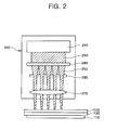
- FIG. 2 is a schematic drawing for explaining a method for fabricating an organic electroluminescence device according to the present invention.
- a substrate 110 on which a pixel electrode is formed is provided. Subsequently, a donor substrate 120 on which an organic layer 130 is formed is laminated on the pixel electrode formed substrate 110. The organic layer 130 formed donor substrate 120 is laminated on the substrate 110 by vacuum adsorption or pressurization roller.
- an organic layer pattern is formed on the pixel electrode formed substrate 110 by irradiating a laser beam 250 onto the donor substrate 120 using a laser irradiation apparatus 200 equipped with a diffractive optical element.
- the laser irradiation apparatus 200 comprises a laser generator 240, a diffractive optical element 280, a patterned mask 260 and a projection lens 270.
- the diffractive optical element 280 is formed under the laser generator 240 and designed in advance to form an organic layer pattern of a desired shape.
- the diffractive optical element 280 as an optical element using diffraction phenomenon of light adjusts the focus of the lens by a method for corresponding phases, wherein the diffractive optical element 280 as an element having thin thickness has the same effect that the laser beam passes through the same optical path in a refraction lens since the laser beam reaches the image point as the same phase although laser beams passing through respective courses do not have the same optical path while a laser beam generated from the laser generator reaches an image point.
- the diffractive optical element 280 has reduced volume and weight due to thin thickness compared with a refraction element, is easily fabricated by a simple fabrication method compared with the refraction element, and reduces fabrication cost by enabling the diffractive optical element 280 to be produced in a mass quantity by a method such as extrusion molding.
- the diffractive optical element 280 diffracts an incidence laser beam 250 generated from the laser generator 240 to a pattern part of the mask 260. Therefore, a laser beam is diffracted by the diffractive optical element 280 such that the diffracted laser beam is irradiated onto the projection lens 270 by passing through the mask in the state that the laser beam is not cut off by the mask differently from that the laser beam is conventionally cut off by the mask. That is, energy efficiency of the laser beam is improved by forming the organic layer pattern without loss of the laser beam 250 generated from the laser generator 240.
- a method for fabricating an organic electroluminescence device 280 according to the present invention simplifies the fabrication process and reduces fabrication cost by fabricating only the mask 260 correspondingly to a desired pattern in the state that the diffractive optical element 280 is remained as it is.
- An organic layer pattern is formed on the substrate 110 by irradiating the laser beam onto the donor substrate 110 after a laser beam 255 diffracted by the diffractive optical element 280 is refracted through the projection lens 270 formed under the diffractive optical element 280.
- a process of forming the organic film layer can be performed at an atmosphere of nitrogen gas (N 2 ).
- the transfer process can be performed at a nitrogen atmosphere from which oxygen is removed since there is the possibility of oxidation of the organic layer pattern to be transferred due to existence of oxygen in an ordinary atmosphere. Furthermore, the transfer process can be performed in a vacuum environment to obtain an effect of suppressing generation of air bubbles between the donor substrate and the substrate during the foregoing laminating process.
- the organic layer pattern formed in the transfer process can be a single layer or multilayer selected from the group consisting of an emitting layer, a hole injection layer, a hole transport layer, an electron transport layer and an electron injection layer.
- An organic electroluminescence device is completed by forming a cathode electrode on the organic layer pattern after performing a transfer process of forming the organic layer pattern.
- a method for fabricating an organic electroluminescence device according to the present invention has merits that energy efficiency of a laser beam is improved by using a diffractive optical element when forming an organic layer pattern by LITI, and fabrication process of the organic electroluminescence device is simplified and fabrication cost of the organic electroluminescence device is reduced by replacing a mask only when forming a laser beam having various shapes to fabricate the organic electroluminescence device.
Landscapes
- Physics & Mathematics (AREA)
- Optics & Photonics (AREA)
- Engineering & Computer Science (AREA)
- Manufacturing & Machinery (AREA)
- Plasma & Fusion (AREA)
- Mechanical Engineering (AREA)
- Electroluminescent Light Sources (AREA)
- Laser Beam Processing (AREA)
Abstract
Description
- This application claims the benefit of Korean Patent Application No. 2004-76674, filed on September 23, 2004, the disclosure of which is hereby incorporated herein by reference in its entirety.
- The present invention relates to a method for fabricating an organic electroluminescence device, more particularly, to a method for forming the organic film layer pattern using a laser irradiation apparatus equipped with a diffractive optical element when forming an organic layer pattern by laser induced thermal imaging (LITI).
- Generally, an organic electroluminescence device that is a flat panel display comprises an anode electrode and a cathode electrode, and organic layers disposed between the anode electrode and the cathode electrode.
- The organic layers comprise at least an emitting layer and further comprise a hole injection layer, a hole transport layer, an electron transport layer and an electron injection layer in addition to the emitting layer. The organic electroluminescence device is classified into a high molecular organic electroluminescence device and a small molecular organic electroluminescence device according to materials composing the organic layers, particularly the emitting layer.
- The emitting layer should be patterned to realize full coloration of the organic electroluminescence device, wherein a method for patterning the emitting layer includes a photolithography process using a shadow mask in case of the small molecular organic electroluminescence device, and an ink-jet printing method or a laser induced thermal imaging (hereinafter referred to as "LITI") method using laser in case of the high molecular organic electroluminescence device. The LITI method has merits that it is capable of patterning the organic layers finely, is applied to a large area and is favorable to high resolution, and the LITI method is a dry process while the ink-jet printing method is a wet process.
- A method for forming patterns of the organic layers by the LITI method requires at least a laser generator, an organic electroluminescence device substrate and a donor substrate. A method of patterning organic layers on the substrate comprises a step of absorbing a laser beam coming out of the laser generator into a light-to-heat conversion layer of the donor substrate such that the laser beam is converted into thermal energy, and a step of transferring a material composing a transfer layer onto the substrate by the thermal energy. The method of patterning organic layers on the substrate is disclosed in Korean Patent Application No. 1998-51844 and United States Patent Nos. 5,998,085, 6,214,520 and 6,114,088.
- FIG. 1 is a schematic drawing for explaining a method for fabricating an organic electroluminescence device according to the prior art.
- Referring to FIG. 1, a
substrate 110 on which a pixel electrode is formed is provided. Subsequently, adonor substrate 120 on which anorganic layer 130 is formed is laminated on the pixel electrode formedsubstrate 110. - An organic layer pattern is formed on the pixel electrode formed
substrate 110 by irradiating a laser beam 150 onto thedonor substrate 120 using a laser irradiation apparatus 100. - The laser irradiation apparatus 100 comprises a laser generator 140, a patterned mask 160 and a projection lens 170. An organic layer pattern is formed on the
substrate 110 by forming a laser beam 150 generated by the laser generator 140 as a pattern having a desired shape through the patterned mask 160 formed on a lower part of the laser generator 140 such that the laser beam 150 is irradiated onto thedonor substrate 110. - All laser beams 150 generated from the laser generator 140 do not pass through the patterned mask 160. That is, although a laser beam irradiated on a patterned part of the mask 160 is irradiated onto the projection lens 170 through the mask 160, a laser beam irradiated on a non-patterned part of the mask 160 is cut off by the mask 160. Therefore, a large amount of laser beam including the laser beam cut off by the mask 160 is required to form the organic layer pattern. After all, there is a problem that efficiency of laser beam is deteriorated.
- Therefore, in order to solve the foregoing problem of the prior art, it is an object of the present invention to provide a method for fabricating an organic electroluminescence device, that is capable of improving energy efficiency of laser beam by using a diffractive optical element when forming an organic layer pattern by LITI and that is capable of reducing cost by forming an organic layer pattern having various shapes in the state that only a mask is replaced.
- In order to achieve the foregoing object, the present invention provides a method for fabricating an organic electroluminescence device comprising a step of providing a substrate on which a pixel electrode is formed, a step of laminating a donor substrate on the front of the substrate, and a step of forming an organic layer pattern on the substrate by irradiating a laser beam onto a predetermined region of the donor substrate using a laser irradiation apparatus equipped with a diffractive optical element.
- The laser irradiation apparatus comprises a laser generator, a diffractive optical element formed under the laser generator to diffract a laser beam generated from the laser generator, a patterned mask formed under the diffractive optical element, and a projection lens formed under the patterned mask.
- The step of forming the organic layer pattern on the pixel electrode is performed at an atmoshphere of nitrogen gas (N2) or in a vacuum environment.
- The organic layer pattern is a single layer or multilayer selected from the group consisting of an emitting layer, a hole injection layer, a hole transport layer, an electron transport layer and an electron injection layer.
- The above and other features and advantages of the present invention will become more apparent to those of ordinary skill in the art by describing in detail preferred embodiments thereof with reference to the attached drawings in which:
- FIG. 1 is a schematic drawing for explaining a method for fabricating an organic electroluminescence device according to the prior art; and
- FIG. 2 is a schematic drawing for explaining a method for fabricating an organic electroluminescence device according to the present invention.
- The present invention will now be described in detail in connection with preferred embodiments with reference to the accompanying drawings. For reference, like reference characters designate corresponding parts throughout several views.
- FIG. 2 is a schematic drawing for explaining a method for fabricating an organic electroluminescence device according to the present invention.
- Referring to FIG. 2, a
substrate 110 on which a pixel electrode is formed is provided. Subsequently, adonor substrate 120 on which anorganic layer 130 is formed is laminated on the pixel electrode formedsubstrate 110. Theorganic layer 130 formeddonor substrate 120 is laminated on thesubstrate 110 by vacuum adsorption or pressurization roller. - Continuously, an organic layer pattern is formed on the pixel electrode formed
substrate 110 by irradiating alaser beam 250 onto thedonor substrate 120 using alaser irradiation apparatus 200 equipped with a diffractive optical element. - The
laser irradiation apparatus 200 comprises alaser generator 240, a diffractiveoptical element 280, apatterned mask 260 and aprojection lens 270. - The diffractive
optical element 280 is formed under thelaser generator 240 and designed in advance to form an organic layer pattern of a desired shape. The diffractiveoptical element 280 as an optical element using diffraction phenomenon of light adjusts the focus of the lens by a method for corresponding phases, wherein the diffractiveoptical element 280 as an element having thin thickness has the same effect that the laser beam passes through the same optical path in a refraction lens since the laser beam reaches the image point as the same phase although laser beams passing through respective courses do not have the same optical path while a laser beam generated from the laser generator reaches an image point. In aspects except optical characteristics, the diffractiveoptical element 280 has reduced volume and weight due to thin thickness compared with a refraction element, is easily fabricated by a simple fabrication method compared with the refraction element, and reduces fabrication cost by enabling the diffractiveoptical element 280 to be produced in a mass quantity by a method such as extrusion molding. - The diffractive
optical element 280 diffracts anincidence laser beam 250 generated from thelaser generator 240 to a pattern part of themask 260. Therefore, a laser beam is diffracted by the diffractiveoptical element 280 such that the diffracted laser beam is irradiated onto theprojection lens 270 by passing through the mask in the state that the laser beam is not cut off by the mask differently from that the laser beam is conventionally cut off by the mask. That is, energy efficiency of the laser beam is improved by forming the organic layer pattern without loss of thelaser beam 250 generated from thelaser generator 240. - Furthermore, fabrication process of the diffractive
optical element 280 becomes complicated, and fabrication cost of the diffractiveoptical element 280 is increased since the diffractiveoptical element 280 should be fabricated again correspondingly to the pattern to form an organic layer pattern of various shapes. However, a method for fabricating anorganic electroluminescence device 280 according to the present invention simplifies the fabrication process and reduces fabrication cost by fabricating only themask 260 correspondingly to a desired pattern in the state that the diffractiveoptical element 280 is remained as it is. - An organic layer pattern is formed on the
substrate 110 by irradiating the laser beam onto thedonor substrate 110 after alaser beam 255 diffracted by the diffractiveoptical element 280 is refracted through theprojection lens 270 formed under the diffractiveoptical element 280. - A process of forming the organic film layer can be performed at an atmosphere of nitrogen gas (N2). The transfer process can be performed at a nitrogen atmosphere from which oxygen is removed since there is the possibility of oxidation of the organic layer pattern to be transferred due to existence of oxygen in an ordinary atmosphere. Furthermore, the transfer process can be performed in a vacuum environment to obtain an effect of suppressing generation of air bubbles between the donor substrate and the substrate during the foregoing laminating process.
- The organic layer pattern formed in the transfer process can be a single layer or multilayer selected from the group consisting of an emitting layer, a hole injection layer, a hole transport layer, an electron transport layer and an electron injection layer.
- An organic electroluminescence device is completed by forming a cathode electrode on the organic layer pattern after performing a transfer process of forming the organic layer pattern.
- As described in the above, a method for fabricating an organic electroluminescence device according to the present invention has merits that energy efficiency of a laser beam is improved by using a diffractive optical element when forming an organic layer pattern by LITI, and fabrication process of the organic electroluminescence device is simplified and fabrication cost of the organic electroluminescence device is reduced by replacing a mask only when forming a laser beam having various shapes to fabricate the organic electroluminescence device.
- While the invention has been particularly shown and described with reference to preferred embodiments thereof, it will be understood by those skilled in the art that the foregoing and other changes in form and details may be made therein without departing from the spirit and scope of the invention.
Claims (5)
- A method for fabricating an organic electroluminescence device comprising:providing a substrate on which a pixel electrode is formed;laminating a donor substrate on the front of the substrate;andforming an organic layer pattern on the substrate by irradiating a laser beam onto a predetermined region of the donor substrate using a laser irradiation apparatus.
- The method according to claim 1, wherein the laser irradiation apparatus comprises a laser generator; a diffractive optical element formed under the laser generator to diffract a laser beam generated from the laser generator; a patterned mask formed under the diffractive optical element; and a projection lens formed under the patterned mask.
- The method according to claim 1, wherein forming the organic layer pattern on the pixel electrode is performed at an atmoshphere of nitrogen gas (N2).
- The method according to claim 1, wherein forming the organic layer pattern on the pixel electrode is performed in a vacuum environment.
- The method according to claim 1, wherein the organic layer pattern is a single layer or multilayer selected from the group consisting of an emitting layer, a hole injection layer, a hole transport layer, an electron transport layer and an electron injection layer.
Applications Claiming Priority (1)
| Application Number | Priority Date | Filing Date | Title |
|---|---|---|---|
| KR1020040076674A KR20060027750A (en) | 2004-09-23 | 2004-09-23 | Manufacturing method of organic electroluminescent element |
Publications (1)
| Publication Number | Publication Date |
|---|---|
| EP1641055A1 true EP1641055A1 (en) | 2006-03-29 |
Family
ID=36074458
Family Applications (1)
| Application Number | Title | Priority Date | Filing Date |
|---|---|---|---|
| EP05108609A Ceased EP1641055A1 (en) | 2004-09-23 | 2005-09-19 | Method for fabricating organic electroluminescence device |
Country Status (6)
| Country | Link |
|---|---|
| US (1) | US20060063099A1 (en) |
| EP (1) | EP1641055A1 (en) |
| JP (1) | JP2006093127A (en) |
| KR (1) | KR20060027750A (en) |
| CN (1) | CN1753587A (en) |
| TW (1) | TWI295514B (en) |
Cited By (1)
| Publication number | Priority date | Publication date | Assignee | Title |
|---|---|---|---|---|
| GB2438600A (en) * | 2006-05-19 | 2007-12-05 | Exitech Ltd | Laser ablation method and tool |
Families Citing this family (8)
| Publication number | Priority date | Publication date | Assignee | Title |
|---|---|---|---|---|
| KR100793360B1 (en) * | 2006-01-16 | 2008-01-11 | 삼성에스디아이 주식회사 | Masks for Laser Irradiation Devices |
| KR100770264B1 (en) | 2006-01-16 | 2007-10-25 | 삼성에스디아이 주식회사 | Laser irradiation apparatus and manufacturing method of organic light emitting device using same |
| KR100793364B1 (en) * | 2006-05-29 | 2008-01-11 | 삼성에스디아이 주식회사 | Laser irradiation apparatus and manufacturing method of organic light emitting device using same |
| KR100793363B1 (en) * | 2006-05-29 | 2008-01-11 | 삼성에스디아이 주식회사 | Laser irradiation apparatus and manufacturing method of organic light emitting device using same |
| KR100796595B1 (en) * | 2006-07-14 | 2008-01-21 | 삼성에스디아이 주식회사 | Laser irradiation apparatus and manufacturing method of organic light emitting device using same |
| KR100796596B1 (en) * | 2006-07-14 | 2008-01-21 | 삼성에스디아이 주식회사 | Laser irradiation apparatus and manufacturing method of organic light emitting device using same |
| KR100796597B1 (en) * | 2006-07-14 | 2008-01-21 | 삼성에스디아이 주식회사 | Laser irradiation apparatus and manufacturing method of organic light emitting device using same |
| JP5656659B2 (en) * | 2011-01-14 | 2015-01-21 | 三菱重工業株式会社 | Manufacturing method of organic EL element |
Citations (3)
| Publication number | Priority date | Publication date | Assignee | Title |
|---|---|---|---|---|
| US20010000744A1 (en) * | 1999-01-15 | 2001-05-03 | 3M Innovative Properties Company | Thermal transfer element and process for forming organic electroluminescent devices |
| EP1335637A1 (en) * | 2002-01-30 | 2003-08-13 | Eastman Kodak Company | Making electroluminescent display devices |
| EP1357590A2 (en) * | 2002-04-25 | 2003-10-29 | Seiko Epson Corporation | Method and apparatus for manufacturing electronic devices |
Family Cites Families (3)
| Publication number | Priority date | Publication date | Assignee | Title |
|---|---|---|---|---|
| US5998085A (en) * | 1996-07-23 | 1999-12-07 | 3M Innovative Properties | Process for preparing high resolution emissive arrays and corresponding articles |
| US6114088A (en) * | 1999-01-15 | 2000-09-05 | 3M Innovative Properties Company | Thermal transfer element for forming multilayer devices |
| JP2002222694A (en) * | 2001-01-25 | 2002-08-09 | Sharp Corp | Laser processing apparatus and organic electroluminescent display panel using the same |
-
2004
- 2004-09-23 KR KR1020040076674A patent/KR20060027750A/en not_active Ceased
-
2005
- 2005-09-15 JP JP2005268536A patent/JP2006093127A/en active Pending
- 2005-09-19 EP EP05108609A patent/EP1641055A1/en not_active Ceased
- 2005-09-19 TW TW094132351A patent/TWI295514B/en not_active IP Right Cessation
- 2005-09-22 US US11/231,750 patent/US20060063099A1/en not_active Abandoned
- 2005-09-23 CN CNA2005101037926A patent/CN1753587A/en active Pending
Patent Citations (3)
| Publication number | Priority date | Publication date | Assignee | Title |
|---|---|---|---|---|
| US20010000744A1 (en) * | 1999-01-15 | 2001-05-03 | 3M Innovative Properties Company | Thermal transfer element and process for forming organic electroluminescent devices |
| EP1335637A1 (en) * | 2002-01-30 | 2003-08-13 | Eastman Kodak Company | Making electroluminescent display devices |
| EP1357590A2 (en) * | 2002-04-25 | 2003-10-29 | Seiko Epson Corporation | Method and apparatus for manufacturing electronic devices |
Cited By (2)
| Publication number | Priority date | Publication date | Assignee | Title |
|---|---|---|---|---|
| GB2438600A (en) * | 2006-05-19 | 2007-12-05 | Exitech Ltd | Laser ablation method and tool |
| GB2438600B (en) * | 2006-05-19 | 2008-07-09 | Exitech Ltd | Method for patterning thin films on moving substrates |
Also Published As
| Publication number | Publication date |
|---|---|
| JP2006093127A (en) | 2006-04-06 |
| US20060063099A1 (en) | 2006-03-23 |
| KR20060027750A (en) | 2006-03-28 |
| TWI295514B (en) | 2008-04-01 |
| CN1753587A (en) | 2006-03-29 |
| TW200620730A (en) | 2006-06-16 |
Similar Documents
| Publication | Publication Date | Title |
|---|---|---|
| EP1667249B1 (en) | Pattering method and method of fabricating organic light emitting display (OLED) using the patterning method | |
| US7999835B2 (en) | Laser irradiation apparatus and method of fabricating organic light emitting display using the same | |
| US8480448B2 (en) | Donor film for laser induced thermal imaging method, light emitting device using the same, and method of manufacturing light emitting device | |
| US20060063099A1 (en) | Method for fabricating organic electroluminescence device | |
| KR100700654B1 (en) | Laser Irradiation Device and Laser Thermal Transfer Method | |
| EP1672716B1 (en) | Apparatus and method of fabricating organic light emitting display using a laser induced thermal printing apparatus | |
| KR100712115B1 (en) | Laser irradiation apparatus and manufacturing method of organic electroluminescent device using the same | |
| US7820340B2 (en) | Laser induced thermal imaging (LITI) mask and an organic electroluminescent device fabrication method using the mask | |
| US8535964B2 (en) | Frame assembly extending donor film, method of manufacturing donor film used in laser induced thermal imaging(LITI), and method of manufacturing organic light emitting device | |
| US7303850B2 (en) | Method of fabricating organic light emitting display | |
| KR100761073B1 (en) | Laser thermal transfer method |
Legal Events
| Date | Code | Title | Description |
|---|---|---|---|
| PUAI | Public reference made under article 153(3) epc to a published international application that has entered the european phase |
Free format text: ORIGINAL CODE: 0009012 |
|
| AK | Designated contracting states |
Kind code of ref document: A1 Designated state(s): AT BE BG CH CY CZ DE DK EE ES FI FR GB GR HU IE IS IT LI LT LU LV MC NL PL PT RO SE SI SK TR |
|
| AX | Request for extension of the european patent |
Extension state: AL BA HR MK YU |
|
| 17P | Request for examination filed |
Effective date: 20060816 |
|
| 17Q | First examination report despatched |
Effective date: 20060922 |
|
| AKX | Designation fees paid |
Designated state(s): DE FR GB |
|
| 17Q | First examination report despatched |
Effective date: 20060922 |
|
| RAP1 | Party data changed (applicant data changed or rights of an application transferred) |
Owner name: SAMSUNG MOBILE DISPLAY CO., LTD. |
|
| STAA | Information on the status of an ep patent application or granted ep patent |
Free format text: STATUS: THE APPLICATION HAS BEEN REFUSED |
|
| 18R | Application refused |
Effective date: 20081217 |