EP1640956A2 - Verfahren und Vorrichtung für MEMS Anzeigetafel - Google Patents
Verfahren und Vorrichtung für MEMS Anzeigetafel Download PDFInfo
- Publication number
- EP1640956A2 EP1640956A2 EP05255680A EP05255680A EP1640956A2 EP 1640956 A2 EP1640956 A2 EP 1640956A2 EP 05255680 A EP05255680 A EP 05255680A EP 05255680 A EP05255680 A EP 05255680A EP 1640956 A2 EP1640956 A2 EP 1640956A2
- Authority
- EP
- European Patent Office
- Prior art keywords
- row
- column
- voltage
- line time
- modulator
- Prior art date
- Legal status (The legal status is an assumption and is not a legal conclusion. Google has not performed a legal analysis and makes no representation as to the accuracy of the status listed.)
- Withdrawn
Links
- 238000000034 method Methods 0.000 title claims description 34
- 230000008569 process Effects 0.000 claims description 7
- 238000004519 manufacturing process Methods 0.000 claims description 4
- 238000006243 chemical reaction Methods 0.000 claims description 3
- 230000008859 change Effects 0.000 abstract description 8
- 238000007667 floating Methods 0.000 abstract description 3
- 230000004913 activation Effects 0.000 description 19
- 238000010586 diagram Methods 0.000 description 13
- 239000000463 material Substances 0.000 description 5
- 230000008901 benefit Effects 0.000 description 4
- 239000000758 substrate Substances 0.000 description 4
- 230000003750 conditioning effect Effects 0.000 description 3
- 230000003247 decreasing effect Effects 0.000 description 3
- 238000003491 array Methods 0.000 description 2
- 239000003990 capacitor Substances 0.000 description 2
- 230000001413 cellular effect Effects 0.000 description 2
- 230000009849 deactivation Effects 0.000 description 2
- 238000000151 deposition Methods 0.000 description 2
- 238000003384 imaging method Methods 0.000 description 2
- 230000007246 mechanism Effects 0.000 description 2
- 229910052751 metal Inorganic materials 0.000 description 2
- 239000002184 metal Substances 0.000 description 2
- 230000003287 optical effect Effects 0.000 description 2
- 230000000007 visual effect Effects 0.000 description 2
- IRLPACMLTUPBCL-KQYNXXCUSA-N 5'-adenylyl sulfate Chemical compound C1=NC=2C(N)=NC=NC=2N1[C@@H]1O[C@H](COP(O)(=O)OS(O)(=O)=O)[C@@H](O)[C@H]1O IRLPACMLTUPBCL-KQYNXXCUSA-N 0.000 description 1
- VYZAMTAEIAYCRO-UHFFFAOYSA-N Chromium Chemical compound [Cr] VYZAMTAEIAYCRO-UHFFFAOYSA-N 0.000 description 1
- 230000002745 absorbent Effects 0.000 description 1
- 239000002250 absorbent Substances 0.000 description 1
- 229910052782 aluminium Inorganic materials 0.000 description 1
- XAGFODPZIPBFFR-UHFFFAOYSA-N aluminium Chemical compound [Al] XAGFODPZIPBFFR-UHFFFAOYSA-N 0.000 description 1
- 238000009638 autodisplay Methods 0.000 description 1
- 230000009286 beneficial effect Effects 0.000 description 1
- 239000000919 ceramic Substances 0.000 description 1
- 229910052804 chromium Inorganic materials 0.000 description 1
- 239000011651 chromium Substances 0.000 description 1
- 239000003086 colorant Substances 0.000 description 1
- 239000002178 crystalline material Substances 0.000 description 1
- 230000008021 deposition Effects 0.000 description 1
- 239000003989 dielectric material Substances 0.000 description 1
- 238000005516 engineering process Methods 0.000 description 1
- 238000005530 etching Methods 0.000 description 1
- 230000001747 exhibiting effect Effects 0.000 description 1
- 239000011521 glass Substances 0.000 description 1
- AMGQUBHHOARCQH-UHFFFAOYSA-N indium;oxotin Chemical compound [In].[Sn]=O AMGQUBHHOARCQH-UHFFFAOYSA-N 0.000 description 1
- 238000001746 injection moulding Methods 0.000 description 1
- 239000004973 liquid crystal related substance Substances 0.000 description 1
- 239000012528 membrane Substances 0.000 description 1
- 239000007769 metal material Substances 0.000 description 1
- 238000005459 micromachining Methods 0.000 description 1
- 238000004806 packaging method and process Methods 0.000 description 1
- 230000000704 physical effect Effects 0.000 description 1
- 239000004033 plastic Substances 0.000 description 1
- 239000005060 rubber Substances 0.000 description 1
- 238000000926 separation method Methods 0.000 description 1
- 238000006467 substitution reaction Methods 0.000 description 1
- 230000001960 triggered effect Effects 0.000 description 1
- 238000007666 vacuum forming Methods 0.000 description 1
- 210000000707 wrist Anatomy 0.000 description 1
Images





Classifications
-
- G—PHYSICS
- G09—EDUCATION; CRYPTOGRAPHY; DISPLAY; ADVERTISING; SEALS
- G09G—ARRANGEMENTS OR CIRCUITS FOR CONTROL OF INDICATING DEVICES USING STATIC MEANS TO PRESENT VARIABLE INFORMATION
- G09G3/00—Control arrangements or circuits, of interest only in connection with visual indicators other than cathode-ray tubes
- G09G3/20—Control arrangements or circuits, of interest only in connection with visual indicators other than cathode-ray tubes for presentation of an assembly of a number of characters, e.g. a page, by composing the assembly by combination of individual elements arranged in a matrix no fixed position being assigned to or needed to be assigned to the individual characters or partial characters
- G09G3/34—Control arrangements or circuits, of interest only in connection with visual indicators other than cathode-ray tubes for presentation of an assembly of a number of characters, e.g. a page, by composing the assembly by combination of individual elements arranged in a matrix no fixed position being assigned to or needed to be assigned to the individual characters or partial characters by control of light from an independent source
- G09G3/3433—Control arrangements or circuits, of interest only in connection with visual indicators other than cathode-ray tubes for presentation of an assembly of a number of characters, e.g. a page, by composing the assembly by combination of individual elements arranged in a matrix no fixed position being assigned to or needed to be assigned to the individual characters or partial characters by control of light from an independent source using light modulating elements actuated by an electric field and being other than liquid crystal devices and electrochromic devices
- G09G3/3466—Control arrangements or circuits, of interest only in connection with visual indicators other than cathode-ray tubes for presentation of an assembly of a number of characters, e.g. a page, by composing the assembly by combination of individual elements arranged in a matrix no fixed position being assigned to or needed to be assigned to the individual characters or partial characters by control of light from an independent source using light modulating elements actuated by an electric field and being other than liquid crystal devices and electrochromic devices based on interferometric effect
-
- G—PHYSICS
- G02—OPTICS
- G02F—OPTICAL DEVICES OR ARRANGEMENTS FOR THE CONTROL OF LIGHT BY MODIFICATION OF THE OPTICAL PROPERTIES OF THE MEDIA OF THE ELEMENTS INVOLVED THEREIN; NON-LINEAR OPTICS; FREQUENCY-CHANGING OF LIGHT; OPTICAL LOGIC ELEMENTS; OPTICAL ANALOGUE/DIGITAL CONVERTERS
- G02F1/00—Devices or arrangements for the control of the intensity, colour, phase, polarisation or direction of light arriving from an independent light source, e.g. switching, gating or modulating; Non-linear optics
- G02F1/01—Devices or arrangements for the control of the intensity, colour, phase, polarisation or direction of light arriving from an independent light source, e.g. switching, gating or modulating; Non-linear optics for the control of the intensity, phase, polarisation or colour
- G02F1/21—Devices or arrangements for the control of the intensity, colour, phase, polarisation or direction of light arriving from an independent light source, e.g. switching, gating or modulating; Non-linear optics for the control of the intensity, phase, polarisation or colour by interference
-
- G—PHYSICS
- G09—EDUCATION; CRYPTOGRAPHY; DISPLAY; ADVERTISING; SEALS
- G09G—ARRANGEMENTS OR CIRCUITS FOR CONTROL OF INDICATING DEVICES USING STATIC MEANS TO PRESENT VARIABLE INFORMATION
- G09G3/00—Control arrangements or circuits, of interest only in connection with visual indicators other than cathode-ray tubes
- G09G3/20—Control arrangements or circuits, of interest only in connection with visual indicators other than cathode-ray tubes for presentation of an assembly of a number of characters, e.g. a page, by composing the assembly by combination of individual elements arranged in a matrix no fixed position being assigned to or needed to be assigned to the individual characters or partial characters
-
- G—PHYSICS
- G02—OPTICS
- G02B—OPTICAL ELEMENTS, SYSTEMS OR APPARATUS
- G02B26/00—Optical devices or arrangements for the control of light using movable or deformable optical elements
- G02B26/001—Optical devices or arrangements for the control of light using movable or deformable optical elements based on interference in an adjustable optical cavity
-
- G—PHYSICS
- G09—EDUCATION; CRYPTOGRAPHY; DISPLAY; ADVERTISING; SEALS
- G09G—ARRANGEMENTS OR CIRCUITS FOR CONTROL OF INDICATING DEVICES USING STATIC MEANS TO PRESENT VARIABLE INFORMATION
- G09G2300/00—Aspects of the constitution of display devices
- G09G2300/06—Passive matrix structure, i.e. with direct application of both column and row voltages to the light emitting or modulating elements, other than LCD or OLED
-
- G—PHYSICS
- G09—EDUCATION; CRYPTOGRAPHY; DISPLAY; ADVERTISING; SEALS
- G09G—ARRANGEMENTS OR CIRCUITS FOR CONTROL OF INDICATING DEVICES USING STATIC MEANS TO PRESENT VARIABLE INFORMATION
- G09G2310/00—Command of the display device
- G09G2310/02—Addressing, scanning or driving the display screen or processing steps related thereto
- G09G2310/0264—Details of driving circuits
- G09G2310/0267—Details of drivers for scan electrodes, other than drivers for liquid crystal, plasma or OLED displays
-
- G—PHYSICS
- G09—EDUCATION; CRYPTOGRAPHY; DISPLAY; ADVERTISING; SEALS
- G09G—ARRANGEMENTS OR CIRCUITS FOR CONTROL OF INDICATING DEVICES USING STATIC MEANS TO PRESENT VARIABLE INFORMATION
- G09G2310/00—Command of the display device
- G09G2310/02—Addressing, scanning or driving the display screen or processing steps related thereto
- G09G2310/0264—Details of driving circuits
- G09G2310/027—Details of drivers for data electrodes, the drivers handling digital grey scale data, e.g. use of D/A converters
-
- G—PHYSICS
- G09—EDUCATION; CRYPTOGRAPHY; DISPLAY; ADVERTISING; SEALS
- G09G—ARRANGEMENTS OR CIRCUITS FOR CONTROL OF INDICATING DEVICES USING STATIC MEANS TO PRESENT VARIABLE INFORMATION
- G09G2310/00—Command of the display device
- G09G2310/02—Addressing, scanning or driving the display screen or processing steps related thereto
- G09G2310/0264—Details of driving circuits
- G09G2310/0289—Details of voltage level shifters arranged for use in a driving circuit
-
- G—PHYSICS
- G09—EDUCATION; CRYPTOGRAPHY; DISPLAY; ADVERTISING; SEALS
- G09G—ARRANGEMENTS OR CIRCUITS FOR CONTROL OF INDICATING DEVICES USING STATIC MEANS TO PRESENT VARIABLE INFORMATION
- G09G2310/00—Command of the display device
- G09G2310/06—Details of flat display driving waveforms
- G09G2310/065—Waveforms comprising zero voltage phase or pause
-
- G—PHYSICS
- G09—EDUCATION; CRYPTOGRAPHY; DISPLAY; ADVERTISING; SEALS
- G09G—ARRANGEMENTS OR CIRCUITS FOR CONTROL OF INDICATING DEVICES USING STATIC MEANS TO PRESENT VARIABLE INFORMATION
- G09G2330/00—Aspects of power supply; Aspects of display protection and defect management
- G09G2330/02—Details of power systems and of start or stop of display operation
- G09G2330/021—Power management, e.g. power saving
Definitions
- Microelectromechanical systems include micro mechanical elements, actuators, and electronics. Micromechanical elements may be created using deposition, etching, and or other micromachining processes that etch away parts of substrates and/or deposited material layers or that add layers to form electrical and electromechanical devices.
- An interferometric modulator may comprise a pair of conductive plates, one or both of which may be partially transparent and capable of relative motion upon application of an appropriate electrical signal.
- One plate may comprise a stationary layer deposited on a substrate, the other plate may comprise a metallic membrane suspended over the stationary layer.
- Such devices have a wide range of applications, and it would be beneficial in the art to utilize and/or modify the characteristics of these types of devices so that their features can be exploited in improving existing products and creating new products that have not yet been developed.
- a display driver comprising a row booster configured to generate a row voltage, a column booster configured to generate a column voltage, an array comprising a plurality of modulator elements, each of the modulator elements being connected to a column electrode and a row electrode and being configured to be driven by the row voltage and the column voltage, wherein a state of the modulator elements in a respective row of the array is configured to be modified during a line time in which the row voltage is connected to the respective row electrode, and a disable module configured to disable one of the boosters during a portion of the line time.
- the row and column boosters may each comprise at least one of a level shifter, DC-DC conversion circuitry, and an operational amplifier.
- the disable module may be configured to disable the column booster during the portion of the line time.
- the row booster may be configured to remain active during the disable portion of the line time to provide a bias voltage on each of the row electrodes.
- the bias voltage may be about 5 volts.
- the display driver may further comprise a data enable module configured to output a reference voltage to the column electrodes of the array during the portion of the line time.
- the disable module may be configured to disable the row booster during the portion of the line time.
- the column booster may be configured to remain active during the portion of the line time and may provide a bias voltage on each of the column electrodes.
- the bias voltage may be about 5 volts.
- the display driver may further comprise a data enable module configured to output a reference voltage to the row electrodes of the array during the portion of the line time.
- the modulator elements comprise bi-stable elements.
- a light modulating display driver comprising means for generating a row voltage, means for generating a column voltage, means for modifying modulator elements in a row of an array during a line time in which the row voltage is connected to the respective row, and means for disabling one of the means for generating a row voltage and the means for generating a column voltage during a portion of the line time.
- Still another embodiment provides a method of updating a display region, the display region comprising a plurality of modulator elements arranged in a row and column configuration, wherein the modulator elements each have an actuated and a released state that may be selected by a voltage difference between a row electrode and a column electrode that are each electronically coupled to respective modulator elements, each of the modulator elements being configured to maintain the state of the modulator element when a voltage within a stability window is applied between the row electrode and the column electrode of the respective modulator element, wherein each row of the modulator element is alloted a line time for changing states of the modulator elements of the respective row.
- the method comprises applying a row voltage to a selected row of modulator elements, applying at least one column voltage to selected columns of modulator elements according to a desired state for the modulator elements of the selected row, and terminating the application of the column voltage prior to the completion of the line time, wherein the state of the modulator elements in the selected row is maintained by a voltage difference between the row voltage and a reference voltage, wherein the voltage difference is within the stability window.
- the reference voltage may be provided by a data enable module.
- the method may further comprise enabling the column level shifterat about the end of the line time.
- a method of manufacturing a display driver comprises forming a row booster configured to generate a row voltage, forming a column booster configured to generate a column voltage, forming an array comprising a plurality of modulator elements, each of the modulator elements being connected to a column electrode and a row electrode and each being configured to be driven by the row voltage and the column voltage, wherein a state of the modulator elements in a respective row of the array is configured to be modified during a row line time in which the row voltage is connected to the respective row electrode, or wherein a state of the modulator elements in a respective column of the array is configured to be modified during a column line time in which the column voltage is connected to the respective column electrode, and forming a disable module configured to disable one of the boosters during a portion of the row or column line time.
- the method may further comprise forming a data enable module configured to output a reference voltage to the column electrodes of the array during the portion of the row or column line time.
- the method may further comprise forming the disable module to be configured to disable the row booster during the portion of the row or column line time.
- the method may further comprise forming the column booster to be configured to remain active during the portion of the row or column line time and to provide a bias voltage on each of the column electrodes.
- the method may further comprise forming the modulator elements to comprise bi-stable elements.
- a display driver may be manufactured by the method.
- a display may also be manufactured comprising the display driver.
- each modulator element may be held at either an actuated or a released state with a common voltage difference. Because modulator elements often require less time to change states than is allotted in a line time, power drawn by an array of modulator elements may be reduced by disabling one or both of a row and column voltage boost module, which are configured to amplify an input power source to a level that is suitable for driving modulator elements. If the column voltage is removed during the latter portion of a line time, for example, the row voltage is set to a level that is sufficient to maintain a voltage difference between the row voltage and the floating column voltage within a stability voltage range during the remainder of the line time.
- rows and columns are not limeted to the conventional connotation of horizontal orientation and vertical orientation, respectively. Although some embodiments maintain this conventional connotation, others do not. In some embodiments rows are vertical and columns are horizontal. In other embodiments rows and columns are neither horizontal nor vertical, and may not be oriented at right angles with respect to one another. As such, herein, the identification as a row versus a column is arbitrary.
- the following detailed description is directed to certain specific embodiments of the invention. However, the invention can be embodied in a multitude of different ways. In this description, reference is made to the drawings wherein like parts are designated with like numerals throughout. As will be apparent from the following description, the invention may be implemented in any device that is configured to display an image, whether in motion (e.g., video) or stationary (e.g., still image), and whether textual or pictorial.
- motion e.g., video
- stationary e.g., still image
- the invention may be implemented in or associated with a variety of electronic devices such as, but not limited to, mobile telephones, wireless devices, personal data assistants (PDAs), hand-held or portable computers, GPS receivers/navigators, cameras, MP3 players, camcorders, game consoles, wrist watches, clocks, calculators, television monitors, flat panel displays, computer monitors, auto displays (e.g., odometer display, etc.), cockpit controls and/or displays, display of camera views (e.g., display of a rear view camera in a vehicle), electronic photographs, electronic billboards or signs, projectors, architectural structures (e.g., tile layouts), packaging, and aesthetic structures (e.g., display of images on a piece of jewelry). More generally, the invention may be implemented in electronic switching devices.
- Transmissive liquid crystal display (LCD) modulators modulate light by controlling the twist and/or alignment of crystalline materials to block or pass light.
- Reflective spatial light modulators exploit various physical effects to control the amount of light reflected to the imaging surface. Examples of such reflective modulators include reflective LCDs, and digital micromirror devices.
- FIG. 1 Another example of a spatial light modulator is an interferometric modulator that modulates light by interference.
- One interferometric modulator display embodiment comprising a reflective MEMS display element is illustrated in Figure 1.
- the pixels are in either a bright or dark state.
- a bi-stable display element In the bright ("on” or “open") state, a bi-stable display element reflects incident light to a user.
- a bi-stable display element When in the dark (“off” or “closed”) state, a bi-stable display element is light absorbing and reflects little light to the user.
- the display 110 may be configured to reflect light in the "off” state and absorb light in the "on” state, i.e., the light reflectance properties of the "on” and “off” states are reversed.
- MEMS pixels can also be configured to reflect only selected colors, producing a color display rather than black and white.
- Figure 1 is an isometric perspective view depicting two adjacent pixels in a row of one embodiment of a visual display, comprising a MEMS interferometric modulator.
- An interferometric modulator display comprises a row/column array of these interferometric modulators.
- Each interferometric modulator includes a pair of mirrors positioned at a distance from each other to form a resonant optical cavity.
- one of the mirrors may be moved between at least two positions. In the first position, the movable mirror is positioned at a first distance from the other mirror so that the interferometric modulator is predominantly reflective. In the second position, the movable mirror is positioned at a different distance, e.g., adjacent to the fixed mirror, such that the interferometric modulator is predominantly absorbing.
- the depicted portion of the pixel array includes two adjacent interferometric modulators 12a and 12b in a row.
- a movable mirror 14a is illustrated in the reflective ("released”, “on”, or “open") position at a predetermined distance from a fixed, partial mirror 16a, 16b.
- the movable mirror 14b of the interferometric modulator 12b is illustrated in the non-reflective, absorbent ("actuated", "off”, or “closed") position adjacent to the partial mirror 16b.
- the fixed mirrors 16a, 16b are electrically conductive, and may be fabricated, for example, by depositing layers of chromium and indium-tin-oxide onto a transparent substrate 18 that are patterned into parallel strips, and may form column electrodes.
- the movable mirrors 14a, 14b along the row may be formed as a series of parallel strips of a deposited metal layer or layers (orthogonal to the column electrodes 16a, 16b) on the substrate 18, with aluminum being one suitable material, and may form row electrodes.
- Figures 2 through 5 illustrate one exemplary process and system for using an array of interferometric modulators in a display application.
- Figure 2 is a system block diagram illustrating one embodiment of an electronic device that may incorporate aspects of the invention.
- the electronic device includes a processor 20 which may be any general purpose single- or multi-chip microprocessor such as an ARM, Pentium® , Pentium II® , Pentium III® , Pentium IV®, Pentium® Pro, an 8051, a MIPS®, a Power PC®, an ALPHA®, or any special purpose microprocessor such as a digital signal processor, microcontroller, or a programmable gate array.
- the processor 20 may be configured to execute one or more software modules.
- the processor may be configured to execute one or more software applications, including a web browser, a telephone application, an email program, or any other software application.
- the processor 20 is also configured to communicate with an array controller 22.
- the array controller 22 includes a row driver circuit 24 and a column driver circuit 26 that provide signals to the array 30.
- the cross section of the array illustrated in Figure 1 is shown by the lines 1-1 in Figure 2.
- Portions of the array controller 22 as well as additional circuitry and functionality may be provided by a graphics controller which is typically connected between the actual display drivers and a general purpose microprocessor.
- Exemplary embodiments of the graphics controller include 69030 or 69455 controllers from Chips and Technology, Inc., the S1D1300 series from Seiko Epson , and the Solomon Systech 1906.
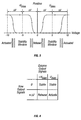
- the row/column actuation protocol may take advantage of a hysteresis property of these devices illustrated in Figure 3. It may require, for example, a 10 volt potential difference to cause a pixel to deform from the released state to the actuated state. However, when the voltage is reduced from that value, the pixel may not release until the voltage drops below 2 volts. There is thus a range of voltage, about 3 to 7 V in the example illustrated in Figure 3, where there exists a stability window within which the device will remain in whatever state it started in.
- the row/column actuation protocol is therefore designed such that during row strobing, pixels in the strobed row that are to be actuated are exposed to a voltage difference of about 10 volts, and pixels that are to be released are exposed to a voltage difference of close to zero volts. After the strobe, the pixels are exposed to a steady state voltage difference of about 5 volts such that they remain in whatever state the row strobe put them in. After being written, each pixel sees a potential difference within the "stability window" of 3-7 volts in this example. This feature makes the pixel design illustrated in Figure 1 stable under the same applied voltage conditions in either an actuated or released pre-existing state.
- each pixel of the interferometric modulator is essentially a capacitor formed by the fixed and moving mirrors, this stable state can be held at a voltage within the hysteresis window with almost no power dissipation. Essentially no current flows into the pixel if the mirror is not moving and the applied potential is fixed.
- a display frame may be created by asserting the set of column electrodes in accordance with the desired set of actuated pixels in the first row.
- a row pulse is then applied to the row 1 electrode, actuating the pixels corresponding to the asserted column lines.
- the asserted set of column electrodes is then changed to correspond to the desired set of actuated pixels in the second row.
- a pulse is then applied to the row 2 electrode, asserting the appropriate pixels in row 2 in accordance with the asserted column electrodes.
- the row 1 pixels are unaffected by the row 2 pulse, and remain in the state they were set to during the row 1 pulse. This may be repeated for the entire series of rows in a sequential fashion to produce the frame.
- the frames are refreshed and/or updated with new display data by continually repeating this process at some desired number of frames per second.
- a wide variety of other protocols for driving row and column electrodes of pixel arrays to produce display frames are also well known and may be used in conjunction with the present invention.
- Figures 4 and 5 illustrate one possible actuation protocol for creating a display frame on the 3x3 array of Figure 2.
- Figure 4 illustrates a possible set of column and row voltage levels that may be used for pixels exhibiting the hysteresis curves of Figure 3.
- actuating a pixel involves setting the appropriate column to -V bias , and the appropriate row to + ⁇ V. Releasing the pixel is accomplished by setting the appropriate column to +V bias , and the appropriate row to the same + ⁇ V. In those rows where the row voltage is held at zero volts, the pixels are stable in whatever state they were originally in, regardless of whether the column is at +V bias , or -V bias .
- Figure 5B is a timing diagram showing a series of row and column signals applied to the 3x3 array of Figure 2 which will result in the display arrangement illustrated in Figure 5A, where actuated pixels are non-reflective.
- the pixels Prior to writing the frame illustrated in Figure 5A, the pixels can be in any state, and in this example, all the rows are at 5 volts, and all the columns are at 10 volts. In this state, all pixels are stable in their existing actuated or released states.
- pixels (1,1), (1,2), (2,2), (3,2) and (3,3) are actuated.
- columns 1 and 2 are set to 0 volts, and column 3 is set to 10 volts. This does not change the state of any pixels, because all the pixels remain in the 3-7 volt stability window.
- Row 1 is then strobed with a pulse that goes from 5 volts, up to 10 volts, and back to 5 volts. This actuates the (1,1) and (1,2) pixels and releases the (1,3) pixel. No other pixels in the array are affected.
- column 2 is set to 0 volts, and columns 1 and 3 are set to 10 volts.
- Row 3 is similarly set by setting columns 2 and 3 to 0 volts, and column 1 to 10 volts.
- the row 3 strobe sets the row 3 pixels as shown in Figure 5A. After writing the frame, the row potentials are zero, and the column potentials can remain at either 10 or 0 volts, and the display is then stable in the arrangement of Figure 5A. It will be appreciated that the same procedure can be employed for arrays of dozens or hundreds of rows and columns. It will also be appreciated that the timing, sequence, and levels of voltages used to perform row and column actuation can be varied widely within the general principles outlined above, and the above example is exemplary only, and any actuation voltage method can be used with the present invention.
- Figures 6A-6C illustrate three different embodiments of the moving mirror structure.
- Figure 6A is a cross section of the embodiment of Figure 1, where a strip of metal material 16 is deposited on orthogonally extending supports 18.
- the moveable mirror is attached to the supports at the corners only, on tethers 32.
- the mirror 16 is suspended from a deformable film 34.
- This embodiment has benefits because the structural design and materials used for the mirror 16 can be optimized with respect to the optical properties, and the structural design and materials used for the deformable layer 34 can be optimized with respect to desired mechanical properties.
- the production of various types of interferometric devices is described in a variety of published documents, including, for example, U.S. Published Application 2004/0051929, which is incorporated by reference in its entirety.
- the electronics that drive the display typically consume a large portion of the total device power and, thus, decreasing the power consumption of driver electronics is desirable.
- Figure 7 is a timing diagram showing a series of row and column signals applied to the 3x3 array of Figure 2, for example, which will result in the display arrangement illustrated in Figure 5A, where actuated pixels are non-reflective.
- the array of modulator elements are each actuated by a voltage difference of about 10 volts, released by a voltage difference of about 0 volts, and maintained at their position by a stability voltage difference in the range of about 3 to 7 volts.
- the row and column voltages may be set to any level that is suitable for driving the modulator elements of the display
- pixels (1,1), (1,2), (2,2), (3,2) and (3,3) are actuated.
- the Row 1 voltage is strobed with a pulse that goes from 5 volts, up to 10 volts, and back to 5 volts.
- Columns 1 and 2 are set to 0 volts and Column 3 is set to 10 volts.
- the (1,1) and (1,2) pixel are actuated (due to the about 10 volts applied across the modulator elements) and the (1,3) pixel is released (due to the about 0 volts applied across the modulator element).
- the Row 1 elements are changed to their desired states, as indicated above, during an activation time 710 in which the row voltage is strobed and the column voltages are set to the appropriate levels according to a data signal 804 (Figure 8).
- the activation time 710 is less than the line time.
- an interferometric modulator needs about 10 microseconds to change states and, therefore, the activation time is set to about 10 microseconds.
- the activation time 710 may be set to any other value that is less than the line time.
- a column level shifter 812 ( Figure 8) that is configured to supply the voltages that are applied to the column terminals may be disabled after the activation time 710, thereby reducing the power drawn from a power source during the column disable time 720.
- Disabling the level shifter may include disconnecting the level shifter 812 from at least one of its power supply, ground supply, and the column load. Other disabling mechanisms are also possible. Some disabling mechanisms may include the use of input data as a signal.
- a data enable module 820 may be configured to ground the column terminals of the array of modulator elements during this column disable time 720. Thus, with 0 volts on each of the columns of the array and 5 volts on the Rows, about 5 volts is applied across each modulator element, maintaining each modulator element in its current state.
- the short pulse module 900 ( Figures 8 and 9) may enable the column level shifter 812 ( Figure 8) near the end of the current line time or similarly near the beginning of a subsequent line time so that the appropriate voltage levels for the next row are provided to the column terminals.
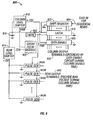
- FIG 8 is a block diagram of an exemplary display driver 800 that is configured to output driver signals for an array of modulator elements of a display device.
- the display driver 800 outputs signals on row output terminals 840 that are coupled to each of the rows of modulator elements and signals on column output terminals 830 that are coupled to each of the columns of modulator elements.
- the display driver 800 disables at least a portion of its circuitry during the column disable time 720, thereby reducing the power consumed by the display driver 800.
- the column output terminals are grounded and the row output terminals 840 provide a bias voltage, e.g., 5 volts.
- the exemplary display device 800 includes a column level shifter 812 and a row level shifter 814, which are each electrically coupled to a power source 806, such as a battery.
- the level shifters 812, 814 are configured to modify the voltage signal supplied by the power source 806 to provide one or more voltage levels that are necessary for driving the modulator elements of the array.
- modulator elements in an exemplary array may require a voltage difference of 10 volts in order to actuate, and a voltage difference of 5 volts to maintain a state.
- the power source 806 provides only 3 volts, the electrical signal from the power source 806 requires boosting in order to provide the voltage levels necessary to actuate modulator elements.
- the voltages for the row terminals such as five and ten volts, are provided by the row level shifter 814 and the voltages for the column terminals, such as five and ten volts, are provided by the column level shifter 814.
- Each of the level shifters 812, 814 may include multiple DC-DC conversion circuitry, operational amplifiers, etc., configured to boost the electrical signal from the power source 816 to one or more desired levels. While the embodiments described herein discuss the use of a voltage booster configured to increase the source voltage to a voltage necessary for driving the modulator elements, those of skill in the art will recognize that in other embodiments the level shifters 812, 814 may be configured to reduce the input voltage to a voltage necessary to drive the modulator elements.
- the exemplary display driver 800 includes a shift register 822 that receives data 824 indicating the desired states of each of the modulator elements in a row of the array.
- the shift register 822 has a width that is equal to the number of columns in the array of modulator elements. Accordingly, the shift register 822 may store data indicative of a next state of an entire row of modulator elements.
- a latch 818 is coupled to the shift register 822 and is configured to receive the data 824 from the shift register 822. In one embodiment, latch 818 outputs the data received from the shift register 822 at the beginning of each line time.
- a data enable module 820 is electrically coupled to the latch 818 and is configured to control when the data should be provided to the column output terminals 830. In one embodiment, the data enable module 820 is configured to output data for a current row of modulator elements during the activation time 710 for that row.
- the data enable module 820 is electrically coupled to the column level shifter 812 so that the appropriate voltage levels are provided to the column output terminals 830.
- the data 824 may contain binary data in the form of 3 volt and 0 volt signals indicative of desired states of modulator elements.
- the data enable module 820 is configured to output a 10 volt signal on each column output terminal 830 that corresponds with a 3 volt signal received from the latch 818. Accordingly, the state of the modulator elements may be stored in the shift register 824 and latch 818 using lower voltage levels than are necessary to change the state of modulator elements.
- a control signal (CTRL) module 702 is coupled to the latch 718 and is configured to provide a horizontal sync output signal indicating when a new line time begins.
- the latch 818 latches the shift register 822 outputs to the latch outputs when the control module 702 indicates that a new line time has started. This data is then passed through the data enable module 820 during the activation time to the column output terminals.
- the exemplary display driver 800 includes a short pulse module 820 that is configured to provide an enable signal that may be used to control the operation of the column level shifter 812 as well as the data enable module 820.
- the short pulse module 820 is configured to disable the column level shifter 814 after the activation time 710 has passed and cause the column level shifter 814 to remain deactivated until the next line time begins. In this way, the column level shifter 814 is disabled for a portion of each line time, the power used by the column level shifter 814 is decreased, and the power consumed by the array of modulator elements is decreased.
- the short pulse module 820 is also coupled to the data enable module 820 and provides a signal indicating when the output to all of the columns should be set to ground.
- the short pulse module 820 may signal to the data enable module 820 that the column output terminals 830 should all be grounded. In this way, the column output terminals 830 are prevented from floating during the disable time 720 while the column level shifter 812 is disabled.
- a bias voltage such as 5 volts, will be maintained on the modulator elements by providing the bias voltage on the row output terminals 840.
- the short pulse module 820 is configured so that deactivation of the column level shifter 812 occurs only after the modulator elements of the current row of the array have had sufficient time to change states, where necessary.
- short pulse module 820 also controls the length of the Row strobe time, e.g., the time that the Row voltage goes to 10 volts in the example of Figure 7, as well as the deactivation of the column level shifter 812.
- Exemplary display driver 800 includes a pulse generator 842 coupled to each of the row output terminals.
- the pulse generators 842 are configured to sequentially provide the row strobe to rows of the array. For example, during a first line time, pulse generator 842A may provide a row strobe to a first row of the array, during a second line time, pulse generator 842B may provide a row strobe to a second row of the array, and so on.
- the control module 802 is electrically coupled to the pulse generators 842 and indicates when each sequential line time begins.
- the Row strobe time is substantially equal to the activation time 710.
- the row output terminals 840 return to a bias voltage,e.g., 5 volts, during the column disable time 720.
- the short pulse module 820 provides an enable signal (not shown) to the pulse generators 842 indicating when the row voltage terminals 740 should be returned to their bias voltage.
- the enable signal from the short pulse module 820 is asserted, both the row and column level shifters 812, 814 are active and the selected pulse generator 842 outputs 10 volts to its respective row output terminal.
- the enable signal when the enable signal is deasserted, such as at the end of activation time 710, the selected pulse generator 842 returns to 5 volts, the column level shifter 812 is disabled, and the data enable grounds the column output terminals 830.
- the enable signal when the enable signal is deasserted, the column level shifter 812 is not active and does not draw power from the power supply 816.
- the short pulse module 820 may comprise various combinations of electrical components that are configured to disable the column boost module 814 after the activation time.
- Figure 9, described in detail below, is a block schematic of one exemplary configuration of components that may be used in a short pulse module 820.
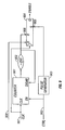
- Figure 9 is a block diagram of an exemplary short pulse module 900 that is configured to output an enable signal, which may be provided to the column level shifter 812 ( Figure 8) in order to control the operation of the level shifter.
- the enable signal may also be transmitted to the pulse generator 842 ( Figure 8) in order to control the row strobe time.
- the exemplary short pulse module 900 includes 3 inputs, an activation signal 908, which provides a desired signal level for the enable signal, a Clock signal (CLK) 1007, and a CTRL signal 902, such as from the CTRL module 802.
- CLK 802 may be a square wave oscillating at 25 MHz, which is a typical VGA data rate. Alternatively, CLK 802 may be any other frequency of clock signal.
- a counter 901 is configured to count every CLK pulse and the CTRL signal 902 input resets the counter 901 to zero at the beginning of each line time.
- a set-reset flip-flop 904 provides the enable output. As those of skill in the art will recognize, the flip-flop 904 is triggered to output the activation signal 908 when the set input 905 is asserted. In one embodiment, when the enable signal is equal to the activation signal 908, the selected Row is strobed and the column level shifter 812 is active. The output of the flip-flop 904 is held until a signal is asserted at a reset input 906.
- a pulse generator 903 may be used to generate a one CLK wide pulse when the CTRL signal 902 is asserted, thus asserting the set signal 905 and configuring the flip-flop 1004 to output the enable signal.
- An equivalence circuit 902 outputs a one CLK wide pulse when the count in the counter 901 is equal to a predetermined value that is representative of the activation time 710.
- the output from the equivalence circuit 902 disables the counter 901, which will be re-enabled when the CTRL signal 902 is next asserted, indicating a new line time.
- the output from the equivalence circuit 902 also asserts the reset input 906, which deasserts the enable signal.
- the short pulse module 900 when the enable signal is deasserted, the output of the short pulse module 900 is equal to zero, the selected Row is returned to a bias voltage, e.g., 5 volts in the embodiment of Figures 7 and 8, the data enable circuit grounds the column electrodes, and the column level shifter 812 is disabled. In this way, the short pulse module 900 controls the time in which column level shifter 812 is active.
- the activation time 710 may be a minimum time required to change states of an interferometric modulator.
- this circuit may be used in conjunction with other types of displays in order to reduce the pulses provided to the displays.
- a short pulse module such as the short pulse module 900, may be coupled to existing display drivers or may be incorporated in the display device.
- Figure 10 is a flow chart illustrating an exemplary method of controlling a level shifter. As described above, by reducing the time that either the row or column level shifter is activated, the total power drawn by a display driver may be reduced and the life of the power supply may be extended.
- data is written to a set of modulator elements in an array of modulator elements.
- an array of modulator elements is refreshed by sequentially updating rows of elements.
- the set of modulator elements comprises one or more rows of modulator elements.
- the set of modulator elements comprises one row of modulator elements.
- the set of modulator elements may comprise a column of elements or any other subset of modulator elements in the array.
- a portion of modulator elements of an array may require less frequent updates than another portion of the array.
- the set of modulator elements may include a portion of only those modulator elements that require more frequent updates.
- one of the level shifters that provide an amplified power signal to the display driver are disabled for a predetermined time.
- the column level shifter 812 is disabled during a column disable time 720.
- the row level shifter may be disabled during a similar portion of each line time.
- the column level shifter may be configured to provide a bias voltage to the modulator elements while the row level shifter is disabled.
- the time during which one of the level shifters is disabled is greater than the time required for the modulator elements in the array to change states.
- the disabled level shifter is re-enabled.
- the column level shifter 812 is re-enabled near the beginning of each line time.
- the column level shifter 812 is able to provide the appropriate voltage levels to the data enable module 820 for setting the state of the modulator elements.
- the column level shifter 812 is enabled prior to the start of a new line time so that the amplified voltage levels are available to the data enable module 820 when the line time begins.
- the column level shifter 812 is enabled after the start of a line time and prior to an activation time, such as activation time 720.
- the row level shifter is re-enabled in block 1030.
- the method returns to block 1010 and repeats blocks 1010, 1020, and 1030 for another set of modulator elements, such as another row of display elements.
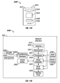
- FIGS 11A and 11B are system block diagrams illustrating an embodiment of a display device 2040.
- the display device 2040 can be, for example, a cellular or mobile telephone.
- the same components of display device 2040 or slight variations thereof are also illustrative of various types of display devices such as televisions and portable media players.
- the display device 2040 includes a housing 2041, a display 2030, an antenna 2043, a speaker 2045, an input device 2048, and a microphone 2046.
- the housing 2041 is generally formed from any of a variety of manufacturing processes as are well known to those of skill in the art, including injection molding, and vacuum forming.
- the housing 2041 may be made from any of a variety of materials, including but not limited to plastic, metal, glass, rubber, and ceramic, or a combination thereof.
- the housing 2041 includes removable portions (not shown) that may be interchanged with other removable portions of different color, or containing different logos, pictures, or symbols.
- the display 2030 of exemplary display device 2040 may be any of a variety of displays, including a bi-stable display, as described herein.
- the display 2030 includes a flat-panel display, such as plasma, EL, OLED, STN LCD, or TFT LCD as described above, or a non-flat-panel display, such as a CRT or other tube device, as is well known to those of skill in the art.
- the display 2030 includes an interferometric modulator display, as described herein.
- the components of one embodiment of exemplary display device 2040 are schematically illustrated in Figure 11B.
- the illustrated exemplary display device 2040 includes a housing 2041 and can include additional components at least partially enclosed therein.
- the exemplary display device 2040 includes a network interface 2027 that includes an antenna 2043 which is coupled to a transceiver 2047.
- the transceiver 2047 is connected to the processor 2021, which is connected to conditioning hardware 2052.
- the conditioning hardware 2052 may be configured to condition a signal (e.g. filter a signal).
- the conditioning hardware 2052 is connected to a speaker 2045 and a microphone 2046.
- the processor 2021 is also connected to an input device 2048 and a driver controller 2029.
- the driver controller 2029 is coupled to a frame buffer 2028 and to the array driver 2022, which in turn is coupled to a display array 2030.
- a power supply 2050 provides power to all components as required by the particular exemplary display device 2040 design.
- the network interface 2027 includes the antenna 2043 and the transceiver 2047 so that the exemplary display device 2040 can communicate with one or more devices over a network. In one embodiment the network interface 2027 may also have some processing capabilities to relieve requirements of the processor 2021.
- the antenna 2043 is any antenna known to those of skill in the art for transmitting and receiving signals. In one embodiment, the antenna transmits and receives RF signals according to the IEEE 802.11 standard, including IEEE 802.11 (a), (b), or (g). In another embodiment, the antenna transmits and receives RF signals according to the BLUETOOTH standard. In the case of a cellular telephone, the antenna is designed to receive CDMA, GSM, AMPS or other known signals that are used to communicate within a wireless cell phone network.
- the transceiver 2047 pre-processes the signals received from the antenna 2043 so that they may be received by and further manipulated by the processor 2021.
- the transceiver 2047 also processes signals received from the processor 2021 so that they may be transmitted from the exemplary display device 2040 via the antenna 2043.
- the transceiver 2047 can be replaced by a receiver.
- network interface 2027 can be replaced by an image source, which can store or generate image data to be sent to the processor 2021.
- the image source can be a digital video disc (DVD) or a hard-disc drive that contains image data, or a software module that generates image data.
Landscapes
- Physics & Mathematics (AREA)
- Engineering & Computer Science (AREA)
- General Physics & Mathematics (AREA)
- Computer Hardware Design (AREA)
- Theoretical Computer Science (AREA)
- Nonlinear Science (AREA)
- Optics & Photonics (AREA)
- Control Of Indicators Other Than Cathode Ray Tubes (AREA)
- Mechanical Light Control Or Optical Switches (AREA)
Applications Claiming Priority (2)
| Application Number | Priority Date | Filing Date | Title |
|---|---|---|---|
| US61341804P | 2004-09-27 | 2004-09-27 | |
| US11/062,143 US20060066594A1 (en) | 2004-09-27 | 2005-02-18 | Systems and methods for driving a bi-stable display element |
Publications (2)
| Publication Number | Publication Date |
|---|---|
| EP1640956A2 true EP1640956A2 (de) | 2006-03-29 |
| EP1640956A3 EP1640956A3 (de) | 2008-09-10 |
Family
ID=35511012
Family Applications (1)
| Application Number | Title | Priority Date | Filing Date |
|---|---|---|---|
| EP05255680A Withdrawn EP1640956A3 (de) | 2004-09-27 | 2005-09-14 | Verfahren und Vorrichtung für MEMS Anzeigetafel |
Country Status (11)
| Country | Link |
|---|---|
| US (1) | US20060066594A1 (de) |
| EP (1) | EP1640956A3 (de) |
| JP (1) | JP2006099079A (de) |
| KR (1) | KR20060092903A (de) |
| AU (1) | AU2005203572A1 (de) |
| BR (1) | BRPI0503874A (de) |
| CA (1) | CA2517325A1 (de) |
| MX (1) | MXPA05009400A (de) |
| RU (1) | RU2005129904A (de) |
| SG (1) | SG121067A1 (de) |
| TW (1) | TW200622992A (de) |
Cited By (3)
| Publication number | Priority date | Publication date | Assignee | Title |
|---|---|---|---|---|
| WO2011084961A1 (en) * | 2010-01-06 | 2011-07-14 | Qualcomm Mems Technologies, Inc. | Charge pump for producing a voltage for a display driver |
| EP3133581A1 (de) * | 2015-08-18 | 2017-02-22 | Ricoh Company, Ltd. | Ansteuersystem, video vorrichtung, bildprojektionsvorrichtung und ansteuerverfahren |
| US9604842B2 (en) | 2014-05-27 | 2017-03-28 | Stmicroelectronics S.R.L. | System for driving an array of MEMS structures and corresponding driving method |
Families Citing this family (43)
| Publication number | Priority date | Publication date | Assignee | Title |
|---|---|---|---|---|
| US7471444B2 (en) * | 1996-12-19 | 2008-12-30 | Idc, Llc | Interferometric modulation of radiation |
| US8928967B2 (en) | 1998-04-08 | 2015-01-06 | Qualcomm Mems Technologies, Inc. | Method and device for modulating light |
| WO1999052006A2 (en) | 1998-04-08 | 1999-10-14 | Etalon, Inc. | Interferometric modulation of radiation |
| US7515147B2 (en) * | 2004-08-27 | 2009-04-07 | Idc, Llc | Staggered column drive circuit systems and methods |
| US7499208B2 (en) | 2004-08-27 | 2009-03-03 | Udc, Llc | Current mode display driver circuit realization feature |
| US7889163B2 (en) * | 2004-08-27 | 2011-02-15 | Qualcomm Mems Technologies, Inc. | Drive method for MEMS devices |
| US7551159B2 (en) * | 2004-08-27 | 2009-06-23 | Idc, Llc | System and method of sensing actuation and release voltages of an interferometric modulator |
| US7560299B2 (en) * | 2004-08-27 | 2009-07-14 | Idc, Llc | Systems and methods of actuating MEMS display elements |
| US8878825B2 (en) * | 2004-09-27 | 2014-11-04 | Qualcomm Mems Technologies, Inc. | System and method for providing a variable refresh rate of an interferometric modulator display |
| US7136213B2 (en) * | 2004-09-27 | 2006-11-14 | Idc, Llc | Interferometric modulators having charge persistence |
| US7843410B2 (en) * | 2004-09-27 | 2010-11-30 | Qualcomm Mems Technologies, Inc. | Method and device for electrically programmable display |
| US7545550B2 (en) * | 2004-09-27 | 2009-06-09 | Idc, Llc | Systems and methods of actuating MEMS display elements |
| US7675669B2 (en) * | 2004-09-27 | 2010-03-09 | Qualcomm Mems Technologies, Inc. | Method and system for driving interferometric modulators |
| CN100439967C (zh) | 2004-09-27 | 2008-12-03 | Idc公司 | 用于多状态干涉光调制的方法和设备 |
| US7626581B2 (en) * | 2004-09-27 | 2009-12-01 | Idc, Llc | Device and method for display memory using manipulation of mechanical response |
| US7679627B2 (en) * | 2004-09-27 | 2010-03-16 | Qualcomm Mems Technologies, Inc. | Controller and driver features for bi-stable display |
| US7446927B2 (en) * | 2004-09-27 | 2008-11-04 | Idc, Llc | MEMS switch with set and latch electrodes |
| US8310441B2 (en) | 2004-09-27 | 2012-11-13 | Qualcomm Mems Technologies, Inc. | Method and system for writing data to MEMS display elements |
| US7724993B2 (en) * | 2004-09-27 | 2010-05-25 | Qualcomm Mems Technologies, Inc. | MEMS switches with deforming membranes |
| US7310179B2 (en) * | 2004-09-27 | 2007-12-18 | Idc, Llc | Method and device for selective adjustment of hysteresis window |
| US7345805B2 (en) * | 2004-09-27 | 2008-03-18 | Idc, Llc | Interferometric modulator array with integrated MEMS electrical switches |
| US7532195B2 (en) * | 2004-09-27 | 2009-05-12 | Idc, Llc | Method and system for reducing power consumption in a display |
| US7948457B2 (en) * | 2005-05-05 | 2011-05-24 | Qualcomm Mems Technologies, Inc. | Systems and methods of actuating MEMS display elements |
| US7920136B2 (en) | 2005-05-05 | 2011-04-05 | Qualcomm Mems Technologies, Inc. | System and method of driving a MEMS display device |
| CA2607807A1 (en) * | 2005-05-05 | 2006-11-16 | Qualcomm Incorporated | Dynamic driver ic and display panel configuration |
| US7355779B2 (en) * | 2005-09-02 | 2008-04-08 | Idc, Llc | Method and system for driving MEMS display elements |
| US20070126673A1 (en) * | 2005-12-07 | 2007-06-07 | Kostadin Djordjev | Method and system for writing data to MEMS display elements |
| US8391630B2 (en) | 2005-12-22 | 2013-03-05 | Qualcomm Mems Technologies, Inc. | System and method for power reduction when decompressing video streams for interferometric modulator displays |
| TWI319556B (en) * | 2005-12-23 | 2010-01-11 | Chi Mei Optoelectronics Corp | Compensation circuit and method for compensate distortion of data signals of liquid crystal display device |
| US7916980B2 (en) | 2006-01-13 | 2011-03-29 | Qualcomm Mems Technologies, Inc. | Interconnect structure for MEMS device |
| US8194056B2 (en) * | 2006-02-09 | 2012-06-05 | Qualcomm Mems Technologies Inc. | Method and system for writing data to MEMS display elements |
| US8049713B2 (en) | 2006-04-24 | 2011-11-01 | Qualcomm Mems Technologies, Inc. | Power consumption optimized display update |
| US7957589B2 (en) * | 2007-01-25 | 2011-06-07 | Qualcomm Mems Technologies, Inc. | Arbitrary power function using logarithm lookup table |
| KR101344819B1 (ko) * | 2007-07-09 | 2013-12-26 | 삼성디스플레이 주식회사 | 전기 영동 표시 장치 |
| BRPI0908803A2 (pt) * | 2008-02-11 | 2015-07-21 | Qualcomm Mems Technologie Inc | Dispositivo e método de sensoreamento, mensuração ou caracterização de elementos de tela integrados com o esquema de drive de tela |
| US8405649B2 (en) * | 2009-03-27 | 2013-03-26 | Qualcomm Mems Technologies, Inc. | Low voltage driver scheme for interferometric modulators |
| US8736590B2 (en) | 2009-03-27 | 2014-05-27 | Qualcomm Mems Technologies, Inc. | Low voltage driver scheme for interferometric modulators |
| US20110109615A1 (en) * | 2009-11-12 | 2011-05-12 | Qualcomm Mems Technologies, Inc. | Energy saving driving sequence for a display |
| JP5310529B2 (ja) * | 2009-12-22 | 2013-10-09 | 株式会社豊田中央研究所 | 板状部材の揺動装置 |
| US20110261046A1 (en) * | 2010-04-22 | 2011-10-27 | Qualcomm Mems Technologies, Inc. | System and method for pixel-level voltage boosting |
| US9057177B2 (en) | 2011-10-08 | 2015-06-16 | Caterpillar Inc. | Implement tooth assembly with tip and adapter |
| US9135843B2 (en) | 2012-05-31 | 2015-09-15 | Qualcomm Mems Technologies, Inc. | Charge pump for producing display driver output |
| JP6805568B2 (ja) * | 2015-08-18 | 2020-12-23 | 株式会社リコー | 駆動システム、画像投影装置および駆動制御方法 |
Citations (3)
| Publication number | Priority date | Publication date | Assignee | Title |
|---|---|---|---|---|
| US6172661B1 (en) | 1994-07-08 | 2001-01-09 | Hitachi, Ltd. | Low power driving method for reducing non-display area of TFT-LCD |
| US20020126364A1 (en) | 1994-05-05 | 2002-09-12 | Iridigm Display Corporation, A Delaware Corporation | Interferometric modulation of radiation |
| US20030072070A1 (en) | 1995-05-01 | 2003-04-17 | Etalon, Inc., A Ma Corporation | Visible spectrum modulator arrays |
Family Cites Families (89)
| Publication number | Priority date | Publication date | Assignee | Title |
|---|---|---|---|---|
| US4441791A (en) * | 1980-09-02 | 1984-04-10 | Texas Instruments Incorporated | Deformable mirror light modulator |
| US4571603A (en) * | 1981-11-03 | 1986-02-18 | Texas Instruments Incorporated | Deformable mirror electrostatic printer |
| US4500171A (en) * | 1982-06-02 | 1985-02-19 | Texas Instruments Incorporated | Process for plastic LCD fill hole sealing |
| US4566935A (en) * | 1984-07-31 | 1986-01-28 | Texas Instruments Incorporated | Spatial light modulator and method |
| US5096279A (en) * | 1984-08-31 | 1992-03-17 | Texas Instruments Incorporated | Spatial light modulator and method |
| US5079544A (en) * | 1989-02-27 | 1992-01-07 | Texas Instruments Incorporated | Standard independent digitized video system |
| US5446479A (en) * | 1989-02-27 | 1995-08-29 | Texas Instruments Incorporated | Multi-dimensional array video processor system |
| US5192946A (en) * | 1989-02-27 | 1993-03-09 | Texas Instruments Incorporated | Digitized color video display system |
| US5206629A (en) * | 1989-02-27 | 1993-04-27 | Texas Instruments Incorporated | Spatial light modulator and memory for digitized video display |
| KR100202246B1 (ko) * | 1989-02-27 | 1999-06-15 | 윌리엄 비. 켐플러 | 디지탈화 비디오 시스템을 위한 장치 및 방법 |
| US5287096A (en) * | 1989-02-27 | 1994-02-15 | Texas Instruments Incorporated | Variable luminosity display system |
| DE69113150T2 (de) * | 1990-06-29 | 1996-04-04 | Texas Instruments Inc | Deformierbare Spiegelvorrichtung mit aktualisiertem Raster. |
| US5083857A (en) * | 1990-06-29 | 1992-01-28 | Texas Instruments Incorporated | Multi-level deformable mirror device |
| US5099353A (en) * | 1990-06-29 | 1992-03-24 | Texas Instruments Incorporated | Architecture and process for integrating DMD with control circuit substrates |
| US5192395A (en) * | 1990-10-12 | 1993-03-09 | Texas Instruments Incorporated | Method of making a digital flexure beam accelerometer |
| US5602671A (en) * | 1990-11-13 | 1997-02-11 | Texas Instruments Incorporated | Low surface energy passivation layer for micromechanical devices |
| CA2063744C (en) * | 1991-04-01 | 2002-10-08 | Paul M. Urbanus | Digital micromirror device architecture and timing for use in a pulse-width modulated display system |
| US5179274A (en) * | 1991-07-12 | 1993-01-12 | Texas Instruments Incorporated | Method for controlling operation of optical systems and devices |
| US5296950A (en) * | 1992-01-31 | 1994-03-22 | Texas Instruments Incorporated | Optical signal free-space conversion board |
| US5312513A (en) * | 1992-04-03 | 1994-05-17 | Texas Instruments Incorporated | Methods of forming multiple phase light modulators |
| JPH0651250A (ja) * | 1992-05-20 | 1994-02-25 | Texas Instr Inc <Ti> | モノリシックな空間的光変調器およびメモリのパッケージ |
| JPH06214169A (ja) * | 1992-06-08 | 1994-08-05 | Texas Instr Inc <Ti> | 制御可能な光学的周期的表面フィルタ |
| US5818095A (en) * | 1992-08-11 | 1998-10-06 | Texas Instruments Incorporated | High-yield spatial light modulator with light blocking layer |
| US5488505A (en) * | 1992-10-01 | 1996-01-30 | Engle; Craig D. | Enhanced electrostatic shutter mosaic modulator |
| US5285196A (en) * | 1992-10-15 | 1994-02-08 | Texas Instruments Incorporated | Bistable DMD addressing method |
| US6674562B1 (en) * | 1994-05-05 | 2004-01-06 | Iridigm Display Corporation | Interferometric modulation of radiation |
| US5489952A (en) * | 1993-07-14 | 1996-02-06 | Texas Instruments Incorporated | Method and device for multi-format television |
| US5619061A (en) * | 1993-07-27 | 1997-04-08 | Texas Instruments Incorporated | Micromechanical microwave switching |
| US5497197A (en) * | 1993-11-04 | 1996-03-05 | Texas Instruments Incorporated | System and method for packaging data into video processor |
| US5598565A (en) * | 1993-12-29 | 1997-01-28 | Intel Corporation | Method and apparatus for screen power saving |
| US6710908B2 (en) * | 1994-05-05 | 2004-03-23 | Iridigm Display Corporation | Controlling micro-electro-mechanical cavities |
| US7550794B2 (en) * | 2002-09-20 | 2009-06-23 | Idc, Llc | Micromechanical systems device comprising a displaceable electrode and a charge-trapping layer |
| US7460291B2 (en) * | 1994-05-05 | 2008-12-02 | Idc, Llc | Separable modulator |
| US6040937A (en) * | 1994-05-05 | 2000-03-21 | Etalon, Inc. | Interferometric modulation |
| US5497172A (en) * | 1994-06-13 | 1996-03-05 | Texas Instruments Incorporated | Pulse width modulation for spatial light modulator with split reset addressing |
| US5499062A (en) * | 1994-06-23 | 1996-03-12 | Texas Instruments Incorporated | Multiplexed memory timing with block reset and secondary memory |
| US5610624A (en) * | 1994-11-30 | 1997-03-11 | Texas Instruments Incorporated | Spatial light modulator with reduced possibility of an on state defect |
| US5612713A (en) * | 1995-01-06 | 1997-03-18 | Texas Instruments Incorporated | Digital micro-mirror device with block data loading |
| US5610438A (en) * | 1995-03-08 | 1997-03-11 | Texas Instruments Incorporated | Micro-mechanical device with non-evaporable getter |
| JP3799092B2 (ja) * | 1995-12-29 | 2006-07-19 | アジレント・テクノロジーズ・インク | 光変調装置及びディスプレイ装置 |
| DE69806846T2 (de) * | 1997-05-08 | 2002-12-12 | Texas Instruments Inc., Dallas | Verbesserungen für räumliche Lichtmodulatoren |
| US5867302A (en) * | 1997-08-07 | 1999-02-02 | Sandia Corporation | Bistable microelectromechanical actuator |
| US6028690A (en) * | 1997-11-26 | 2000-02-22 | Texas Instruments Incorporated | Reduced micromirror mirror gaps for improved contrast ratio |
| US6180428B1 (en) * | 1997-12-12 | 2001-01-30 | Xerox Corporation | Monolithic scanning light emitting devices using micromachining |
| JP4074714B2 (ja) * | 1998-09-25 | 2008-04-09 | 富士フイルム株式会社 | アレイ型光変調素子及び平面ディスプレイの駆動方法 |
| US6391675B1 (en) * | 1998-11-25 | 2002-05-21 | Raytheon Company | Method and apparatus for switching high frequency signals |
| TW523727B (en) * | 1999-05-27 | 2003-03-11 | Koninkl Philips Electronics Nv | Display device |
| US6201633B1 (en) * | 1999-06-07 | 2001-03-13 | Xerox Corporation | Micro-electromechanical based bistable color display sheets |
| US6862029B1 (en) * | 1999-07-27 | 2005-03-01 | Hewlett-Packard Development Company, L.P. | Color display system |
| US6507330B1 (en) * | 1999-09-01 | 2003-01-14 | Displaytech, Inc. | DC-balanced and non-DC-balanced drive schemes for liquid crystal devices |
| WO2003007049A1 (en) * | 1999-10-05 | 2003-01-23 | Iridigm Display Corporation | Photonic mems and structures |
| US6674090B1 (en) * | 1999-12-27 | 2004-01-06 | Xerox Corporation | Structure and method for planar lateral oxidation in active |
| US6466358B2 (en) * | 1999-12-30 | 2002-10-15 | Texas Instruments Incorporated | Analog pulse width modulation cell for digital micromechanical device |
| AU2001272094A1 (en) * | 2000-03-01 | 2001-09-12 | British Telecommunications Public Limited Company | Data transfer method and apparatus |
| US6356085B1 (en) * | 2000-05-09 | 2002-03-12 | Pacesetter, Inc. | Method and apparatus for converting capacitance to voltage |
| JP3843703B2 (ja) * | 2000-06-13 | 2006-11-08 | 富士ゼロックス株式会社 | 光書き込み型記録表示装置 |
| US6853129B1 (en) * | 2000-07-28 | 2005-02-08 | Candescent Technologies Corporation | Protected substrate structure for a field emission display device |
| US6859218B1 (en) * | 2000-11-07 | 2005-02-22 | Hewlett-Packard Development Company, L.P. | Electronic display devices and methods |
| WO2002061781A1 (en) * | 2001-01-30 | 2002-08-08 | Advantest Corporation | Switch and integrated circuit device |
| JP4032216B2 (ja) * | 2001-07-12 | 2008-01-16 | ソニー株式会社 | 光学多層構造体およびその製造方法、並びに光スイッチング素子および画像表示装置 |
| US6862022B2 (en) * | 2001-07-20 | 2005-03-01 | Hewlett-Packard Development Company, L.P. | Method and system for automatically selecting a vertical refresh rate for a video display monitor |
| US6797063B2 (en) * | 2001-10-01 | 2004-09-28 | Fsi International, Inc. | Dispensing apparatus |
| US6870581B2 (en) * | 2001-10-30 | 2005-03-22 | Sharp Laboratories Of America, Inc. | Single panel color video projection display using reflective banded color falling-raster illumination |
| US6791735B2 (en) * | 2002-01-09 | 2004-09-14 | The Regents Of The University Of California | Differentially-driven MEMS spatial light modulator |
| US6791441B2 (en) * | 2002-05-07 | 2004-09-14 | Raytheon Company | Micro-electro-mechanical switch, and methods of making and using it |
| US7256795B2 (en) * | 2002-07-31 | 2007-08-14 | Ati Technologies Inc. | Extended power management via frame modulation control |
| TW544787B (en) * | 2002-09-18 | 2003-08-01 | Promos Technologies Inc | Method of forming self-aligned contact structure with locally etched gate conductive layer |
| US6829132B2 (en) * | 2003-04-30 | 2004-12-07 | Hewlett-Packard Development Company, L.P. | Charge control of micro-electromechanical device |
| US7190380B2 (en) * | 2003-09-26 | 2007-03-13 | Hewlett-Packard Development Company, L.P. | Generating and displaying spatially offset sub-frames |
| US7173314B2 (en) * | 2003-08-13 | 2007-02-06 | Hewlett-Packard Development Company, L.P. | Storage device having a probe and a storage cell with moveable parts |
| US20050057442A1 (en) * | 2003-08-28 | 2005-03-17 | Olan Way | Adjacent display of sequential sub-images |
| US20050068583A1 (en) * | 2003-09-30 | 2005-03-31 | Gutkowski Lawrence J. | Organizing a digital image |
| US6861277B1 (en) * | 2003-10-02 | 2005-03-01 | Hewlett-Packard Development Company, L.P. | Method of forming MEMS device |
| US7560299B2 (en) * | 2004-08-27 | 2009-07-14 | Idc, Llc | Systems and methods of actuating MEMS display elements |
| US7551159B2 (en) * | 2004-08-27 | 2009-06-23 | Idc, Llc | System and method of sensing actuation and release voltages of an interferometric modulator |
| US7515147B2 (en) * | 2004-08-27 | 2009-04-07 | Idc, Llc | Staggered column drive circuit systems and methods |
| US7889163B2 (en) * | 2004-08-27 | 2011-02-15 | Qualcomm Mems Technologies, Inc. | Drive method for MEMS devices |
| US7499208B2 (en) * | 2004-08-27 | 2009-03-03 | Udc, Llc | Current mode display driver circuit realization feature |
| US7602375B2 (en) * | 2004-09-27 | 2009-10-13 | Idc, Llc | Method and system for writing data to MEMS display elements |
| US7724993B2 (en) * | 2004-09-27 | 2010-05-25 | Qualcomm Mems Technologies, Inc. | MEMS switches with deforming membranes |
| US7446927B2 (en) * | 2004-09-27 | 2008-11-04 | Idc, Llc | MEMS switch with set and latch electrodes |
| US7675669B2 (en) * | 2004-09-27 | 2010-03-09 | Qualcomm Mems Technologies, Inc. | Method and system for driving interferometric modulators |
| US8878825B2 (en) * | 2004-09-27 | 2014-11-04 | Qualcomm Mems Technologies, Inc. | System and method for providing a variable refresh rate of an interferometric modulator display |
| US7843410B2 (en) * | 2004-09-27 | 2010-11-30 | Qualcomm Mems Technologies, Inc. | Method and device for electrically programmable display |
| US8310441B2 (en) * | 2004-09-27 | 2012-11-13 | Qualcomm Mems Technologies, Inc. | Method and system for writing data to MEMS display elements |
| CN100439967C (zh) * | 2004-09-27 | 2008-12-03 | Idc公司 | 用于多状态干涉光调制的方法和设备 |
| US7136213B2 (en) * | 2004-09-27 | 2006-11-14 | Idc, Llc | Interferometric modulators having charge persistence |
| US7532195B2 (en) * | 2004-09-27 | 2009-05-12 | Idc, Llc | Method and system for reducing power consumption in a display |
| US7545550B2 (en) * | 2004-09-27 | 2009-06-09 | Idc, Llc | Systems and methods of actuating MEMS display elements |
-
2005
- 2005-02-18 US US11/062,143 patent/US20060066594A1/en not_active Abandoned
- 2005-08-09 AU AU2005203572A patent/AU2005203572A1/en not_active Abandoned
- 2005-08-22 SG SG200505319A patent/SG121067A1/en unknown
- 2005-08-25 JP JP2005243832A patent/JP2006099079A/ja active Pending
- 2005-08-26 CA CA002517325A patent/CA2517325A1/en not_active Abandoned
- 2005-09-02 MX MXPA05009400A patent/MXPA05009400A/es not_active Application Discontinuation
- 2005-09-06 TW TW094130562A patent/TW200622992A/zh unknown
- 2005-09-14 EP EP05255680A patent/EP1640956A3/de not_active Withdrawn
- 2005-09-26 BR BRPI0503874-0A patent/BRPI0503874A/pt not_active IP Right Cessation
- 2005-09-26 KR KR1020050089439A patent/KR20060092903A/ko not_active Withdrawn
- 2005-09-26 RU RU2005129904/09A patent/RU2005129904A/ru not_active Application Discontinuation
Patent Citations (3)
| Publication number | Priority date | Publication date | Assignee | Title |
|---|---|---|---|---|
| US20020126364A1 (en) | 1994-05-05 | 2002-09-12 | Iridigm Display Corporation, A Delaware Corporation | Interferometric modulation of radiation |
| US6172661B1 (en) | 1994-07-08 | 2001-01-09 | Hitachi, Ltd. | Low power driving method for reducing non-display area of TFT-LCD |
| US20030072070A1 (en) | 1995-05-01 | 2003-04-17 | Etalon, Inc., A Ma Corporation | Visible spectrum modulator arrays |
Cited By (8)
| Publication number | Priority date | Publication date | Assignee | Title |
|---|---|---|---|---|
| WO2011084961A1 (en) * | 2010-01-06 | 2011-07-14 | Qualcomm Mems Technologies, Inc. | Charge pump for producing a voltage for a display driver |
| CN102714022A (zh) * | 2010-01-06 | 2012-10-03 | 高通Mems科技公司 | 用于产生显示器驱动器电压的电荷泵 |
| US8884940B2 (en) | 2010-01-06 | 2014-11-11 | Qualcomm Mems Technologies, Inc. | Charge pump for producing display driver output |
| CN102714022B (zh) * | 2010-01-06 | 2015-06-10 | 高通Mems科技公司 | 用于产生显示器驱动器电压的电荷泵 |
| US9604842B2 (en) | 2014-05-27 | 2017-03-28 | Stmicroelectronics S.R.L. | System for driving an array of MEMS structures and corresponding driving method |
| US10118819B2 (en) | 2014-05-27 | 2018-11-06 | Stmicroelectronics S.R.L. | System for driving an array of MEMS structures and corresponding driving method |
| EP3133581A1 (de) * | 2015-08-18 | 2017-02-22 | Ricoh Company, Ltd. | Ansteuersystem, video vorrichtung, bildprojektionsvorrichtung und ansteuerverfahren |
| US10048490B2 (en) | 2015-08-18 | 2018-08-14 | Ricoh Company, Ltd. | Drive system, video device, image projection device, and drive control method |
Also Published As
| Publication number | Publication date |
|---|---|
| CA2517325A1 (en) | 2006-03-27 |
| AU2005203572A1 (en) | 2006-04-13 |
| TW200622992A (en) | 2006-07-01 |
| SG121067A1 (en) | 2006-04-26 |
| BRPI0503874A (pt) | 2006-05-09 |
| KR20060092903A (ko) | 2006-08-23 |
| US20060066594A1 (en) | 2006-03-30 |
| MXPA05009400A (es) | 2006-03-29 |
| RU2005129904A (ru) | 2007-04-10 |
| JP2006099079A (ja) | 2006-04-13 |
| EP1640956A3 (de) | 2008-09-10 |
Similar Documents
| Publication | Publication Date | Title |
|---|---|---|
| EP1640956A2 (de) | Verfahren und Vorrichtung für MEMS Anzeigetafel | |
| EP2383723A1 (de) | Vorrichtung und Verfahren zur Bildanzeige | |
| US7719500B2 (en) | Reflective display pixels arranged in non-rectangular arrays | |
| US7515147B2 (en) | Staggered column drive circuit systems and methods | |
| EP1800282B1 (de) | System und verfahren zur bereitstellung einer variablen auffrischrate eines interferometrischen modulator-displays | |
| US8085461B2 (en) | Systems and methods of actuating MEMS display elements | |
| TWI529685B (zh) | 顯示器及其方法、系統及伺服器 | |
| EP1640950A2 (de) | MEMS-Anzeigevorrichtung und dafür geeignetes Datenschreibverfahren | |
| EP1640953A2 (de) | Methode und System zur Verringerung des Energieverbrauchs in einer Anzeige | |
| US20060066596A1 (en) | System and method of transmitting video data | |
| KR20060092906A (ko) | 간섭 변조기에서의 다중 레벨 밝기를 위한 시스템 및 방법 | |
| KR20060092929A (ko) | 기계적 응답의 조작을 이용한 디스플레이 메모리를 위한기기 및 방법 | |
| US20070126673A1 (en) | Method and system for writing data to MEMS display elements | |
| CN101010714B (zh) | 激活微机电系统显示元件的系统和方法 | |
| US8194056B2 (en) | Method and system for writing data to MEMS display elements | |
| CN100418002C (zh) | 交错的列驱动电路装置及方法 | |
| CN100585675C (zh) | 显示设备、显示驱动器和制造所述驱动器和更新显示区域的方法 | |
| JP4768346B2 (ja) | ディスプレイ素子の列ずらし駆動回路システム及び方法 | |
| HK1086377A (en) | Display apparatus, display driver and method of manufacturing the driver and updating the display region | |
| HK1102840A (en) | Systems and methods of actuating mems display elements |
Legal Events
| Date | Code | Title | Description |
|---|---|---|---|
| PUAI | Public reference made under article 153(3) epc to a published international application that has entered the european phase |
Free format text: ORIGINAL CODE: 0009012 |
|
| AK | Designated contracting states |
Kind code of ref document: A2 Designated state(s): AT BE BG CH CY CZ DE DK EE ES FI FR GB GR HU IE IS IT LI LT LU LV MC NL PL PT RO SE SI SK TR |
|
| AX | Request for extension of the european patent |
Extension state: AL BA HR MK YU |
|
| PUAL | Search report despatched |
Free format text: ORIGINAL CODE: 0009013 |
|
| AK | Designated contracting states |
Kind code of ref document: A3 Designated state(s): AT BE BG CH CY CZ DE DK EE ES FI FR GB GR HU IE IS IT LI LT LU LV MC NL PL PT RO SE SI SK TR |
|
| AX | Request for extension of the european patent |
Extension state: AL BA HR MK YU |
|
| 17P | Request for examination filed |
Effective date: 20090310 |
|
| AKX | Designation fees paid |
Designated state(s): AT BE BG CH CY CZ DE DK EE ES FI FR GB GR HU IE IS IT LI LT LU LV MC NL PL PT RO SE SI SK TR |
|
| RAP1 | Party data changed (applicant data changed or rights of an application transferred) |
Owner name: QUALCOMM MEMS TECHNOLOGIES, INC. |
|
| 17Q | First examination report despatched |
Effective date: 20101005 |
|
| STAA | Information on the status of an ep patent application or granted ep patent |
Free format text: STATUS: THE APPLICATION IS DEEMED TO BE WITHDRAWN |
|
| 18D | Application deemed to be withdrawn |
Effective date: 20110216 |