EP1636856B1 - Ultra thin back-illuminated photodiode array structures and fabrication methods - Google Patents
Ultra thin back-illuminated photodiode array structures and fabrication methods Download PDFInfo
- Publication number
- EP1636856B1 EP1636856B1 EP04777237A EP04777237A EP1636856B1 EP 1636856 B1 EP1636856 B1 EP 1636856B1 EP 04777237 A EP04777237 A EP 04777237A EP 04777237 A EP04777237 A EP 04777237A EP 1636856 B1 EP1636856 B1 EP 1636856B1
- Authority
- EP
- European Patent Office
- Prior art keywords
- substrate
- conductivity type
- regions
- matrix
- photodiode array
- Prior art date
- Legal status (The legal status is an assumption and is not a legal conclusion. Google has not performed a legal analysis and makes no representation as to the accuracy of the status listed.)
- Expired - Lifetime
Links
- 238000000034 method Methods 0.000 title claims abstract description 21
- 238000004519 manufacturing process Methods 0.000 title claims abstract description 10
- 239000000758 substrate Substances 0.000 claims abstract description 67
- 239000011159 matrix material Substances 0.000 claims abstract 22
- 238000009792 diffusion process Methods 0.000 claims description 32
- 238000002513 implantation Methods 0.000 claims description 10
- XUIMIQQOPSSXEZ-UHFFFAOYSA-N Silicon Chemical compound [Si] XUIMIQQOPSSXEZ-UHFFFAOYSA-N 0.000 claims description 7
- 229910052710 silicon Inorganic materials 0.000 claims description 7
- 239000010703 silicon Substances 0.000 claims description 7
- 239000004065 semiconductor Substances 0.000 claims description 6
- 238000003491 array Methods 0.000 abstract description 13
- 235000012431 wafers Nutrition 0.000 description 22
- 239000002184 metal Substances 0.000 description 9
- 239000007943 implant Substances 0.000 description 8
- 239000000463 material Substances 0.000 description 7
- 239000002019 doping agent Substances 0.000 description 6
- 239000000969 carrier Substances 0.000 description 5
- 230000005684 electric field Effects 0.000 description 3
- 238000005516 engineering process Methods 0.000 description 3
- 241001133184 Colletotrichum agaves Species 0.000 description 2
- 238000013459 approach Methods 0.000 description 2
- 230000035945 sensitivity Effects 0.000 description 2
- 229910000679 solder Inorganic materials 0.000 description 2
- 230000004913 activation Effects 0.000 description 1
- 230000015556 catabolic process Effects 0.000 description 1
- 239000013078 crystal Substances 0.000 description 1
- 238000003384 imaging method Methods 0.000 description 1
- 238000002955 isolation Methods 0.000 description 1
- 230000000873 masking effect Effects 0.000 description 1
- 238000005498 polishing Methods 0.000 description 1
- 230000005855 radiation Effects 0.000 description 1
- 230000003595 spectral effect Effects 0.000 description 1
- 230000002123 temporal effect Effects 0.000 description 1
Images





Classifications
-
- H—ELECTRICITY
- H10—SEMICONDUCTOR DEVICES; ELECTRIC SOLID-STATE DEVICES NOT OTHERWISE PROVIDED FOR
- H10F—INORGANIC SEMICONDUCTOR DEVICES SENSITIVE TO INFRARED RADIATION, LIGHT, ELECTROMAGNETIC RADIATION OF SHORTER WAVELENGTH OR CORPUSCULAR RADIATION
- H10F39/00—Integrated devices, or assemblies of multiple devices, comprising at least one element covered by group H10F30/00, e.g. radiation detectors comprising photodiode arrays
- H10F39/10—Integrated devices
- H10F39/107—Integrated devices having multiple elements covered by H10F30/00 in a repetitive configuration, e.g. radiation detectors comprising photodiode arrays
-
- H—ELECTRICITY
- H10—SEMICONDUCTOR DEVICES; ELECTRIC SOLID-STATE DEVICES NOT OTHERWISE PROVIDED FOR
- H10F—INORGANIC SEMICONDUCTOR DEVICES SENSITIVE TO INFRARED RADIATION, LIGHT, ELECTROMAGNETIC RADIATION OF SHORTER WAVELENGTH OR CORPUSCULAR RADIATION
- H10F39/00—Integrated devices, or assemblies of multiple devices, comprising at least one element covered by group H10F30/00, e.g. radiation detectors comprising photodiode arrays
- H10F39/10—Integrated devices
- H10F39/12—Image sensors
- H10F39/199—Back-illuminated image sensors
Definitions
- the present invention relates to semiconductor photodiodes, and in particular, to the structures of high performance, back-illuminated photodiode arrays and the methods of fabricating such structures.
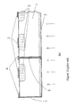
- Figure 1a is a simplified cross section of an exemplary prior art front illuminated photodiode array
- Figure 1b is a simplified cross section of an exemplary prior art back illuminated photodiode array.
- the substrate 1 may be either n-type or p-type material, with opposite conductivity type diffused regions 2 therein. This creates a p-on-n or n-on-p structure, respectively.
- the anode metal pads 3 for the p-on-n structure (the cathode contacts for the n-on-p structure) are always on the device front surface.
- the opposite polarity electrode is usually deposited (plated, sputtered, or evaporated) on the chip back side in the case of the front illuminated structure (see metal layer 4, Figure 1a ), or is made on the device front surface (see metal pads 4, Figure 1b ) using metallized through vias 6, 7 in the case of the back illuminated structure.
- the blanket-type implantation 5 of the back surface of the die of the same conductivity type as the substrate improves both the charge collection efficiency and DC/AC electrical performance of the devices.
- US 4,144,096 is an example of a monolithic solar battery in which wiring for electrically connecting solar cells is provided on upper and lower surfaces of the substrate.
- US 5,670,383 discloses a method of forming an array of avalanche photodiodes.
- US 2002/0011639 discloses a semiconductor imaging device including a substrate having first and second opposing surfaces, and a circuit layer. The substrate is doped to exhibit a first conductivity type. A conducting layer of the substrate includes a first type dopant incorporated near the surface. A region of the substrate includes a heavily doped area within the substrate near the second surface. A plurality of doped regions of the substrate include a second type of dopants formed on the second surface.
- the circuit layer provides gate contacts and readout circuits.
- a back illuminated photodiode array according to claim 1 there is provided a back illuminated photodiode array according to claim 1, and a method of fabricating a back illuminated photodiode array according to claim 13.
- Another object is to provide a method of fabricating si devices on ultra thin wafers, which method can be suitable for fabrication of flip-chip, multi-element, 2-dimensional arrays of silicon photodiodes.
- Figure 2 is a simplified cross-sectional view of a semiconductor ultra-thin chip photodiode array in accordance with a preferred embodiment.
- the structure is built using either n-type or p-type bulk silicon 1.
- the anode in the case of p-on-n structure or the cathode in the case of n-on-p structure will be referred to as "the first electrode”
- the cathode in the case of p-on-n structure and the anode in the case of n-on-p structure will be referred to as "the second electrode.”
- the material resistivity, thickness of the wafer/die, dopants concentrations and doses, and diffusion conditions are preferably chosen to satisfy the following requirements:
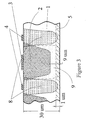
- FIG. 3 An example of a real structure built using a n-type bulk Si with the resistivity of approximately 400 ohm-cm is shown schematically in Figure 3 .
- the width of a depletion region is approximately 9 ⁇ m and extends up to and into (but not through) the blanket implantation 5 in the wafer back side. (See the hatched with dots area 9 in Figure 3 .
- the blanket diffusion 5 is only approximately 0.6 ⁇ m thick, so the depletion region extends approximately to, but not quite all the way to, the wafer back side.)
- the built-in potential creates an electric field across the depletion region and facilitates rapid collection of non-equilibrium carriers created by light near the back surface of the die.
- the non-equilibrium carriers have no or very little possibility of being collected by the electrodes from adjacent cells because:
- the electric field near the die back surface, where the carriers photo-generation predominantly occurs is directed perpendicular to the die surface; therefore, the carriers move (drift) primarily toward the junction of the same cell, having almost no possibility of being trapped by an adjacent cell;
- the second electrode diffusion region 8 which is n+ diffusion in the case of Figure 3 , spans the entire thickness of the die and acts as an effective carrier isolator from adjacent cells.
- the first electrode diffusion 2 may overlap with the second electrode diffusion 8 close to the front surface of the die as shown in Figure 3 . This overlapping may significantly decrease the breakdown voltage, which is not important for a zero bias device.
- first electrode 2 and second electrode 8 are shown in Figure 3 .
- the depth of the first electrode diffusion 2 should be less than the finished substrate thickness (typically less than 50 ⁇ m, and more typically approximately 30 ⁇ m as shown in Figure 3 ) by an amount that approximately equals the depletion depth for the substrate material 1 at zero bias.
- the second electrode diffusion 8 should span the entire thickness of the substrate, or at least to a sufficient depth to provide a reliable low resistance contact with the blanket implantation 5 of the back side of the wafer. Note that the dopants 5 and 8 are of the same polarity.
- Such a structure may be fabricated starting with a thicker substrate (for example 300 ⁇ m) for structural stiffness and integrity during the processing, using three masking steps:
- the array is then reduced in thickness by grinding the back side of the array, preferably to provide a substrate thickness of under approximately 50 ⁇ m, and more preferably to approximately 30 ⁇ m.
- the final thickness achieved is preferably selected in accordance with the resistivity of the substrate and the depth of the first electrode diffusion so that the diffusion is spaced away form the back side of the substrate an amount that approximately equals the depletion depth for the substrate material at zero bias.
- a blanket implant of the first conductivity type is made to the back side of the wafer, which implant improves both the charge collection efficiency and DC/AC electrical performance of the photodiode arrays. Activation of the implant does not significantly alter the first and second electrode diffusions.
- a diffusion for the back side could be used if desired.
- the blanket implant is quite thin compared to the depletion region, with the depletion region extending into, but not through, the blanket implant in the final array.
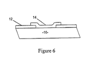
- the oxide layer 12 is evenly patterned and the metal pads 14 contacting the first electrode 2 and second electrode 8 are evenly spaced across the surface of the die 16 and made the same size to provide identical ball bumping conditions throughout the wafer (see Figures 5 and 6 ).
- the oxide layer 12 and metal pads 14 are represented by the larger diameter circles in Figure 5 , with the smaller diameter circles describing the contact openings.
- the present photodiode arrays exhibit very low cross talk because of the excellent isolation of each pixel. Also, because of the small depletion volume, the arrays exhibit low noise and low temperature sensitivity. When used in X-ray systems, they exhibit low radiation damage, and have thermal characteristics similar to scintillators to which they will are mounted.
- the technique of using a deep diffusion in conjunction with a thin substrate for making electrical contact to the back side of the substrate may, of course be used in other semiconductor devices. While the deep diffusion in the current invention is of the same conductivity type as the substrate, the deep diffusion may be of the opposite conductivity type in an alternative device, if desired.
Landscapes
- Light Receiving Elements (AREA)
- Solid State Image Pick-Up Elements (AREA)
Abstract
Description
- The present invention relates to semiconductor photodiodes, and in particular, to the structures of high performance, back-illuminated photodiode arrays and the methods of fabricating such structures.
- Conventional photodiode array structures are based on either front illuminated or back illuminated technologies.
Figure 1a is a simplified cross section of an exemplary prior art front illuminated photodiode array andFigure 1b is a simplified cross section of an exemplary prior art back illuminated photodiode array. Thesubstrate 1 may be either n-type or p-type material, with opposite conductivity type diffusedregions 2 therein. This creates a p-on-n or n-on-p structure, respectively. Theanode metal pads 3 for the p-on-n structure (the cathode contacts for the n-on-p structure) are always on the device front surface. The opposite polarity electrode is usually deposited (plated, sputtered, or evaporated) on the chip back side in the case of the front illuminated structure (seemetal layer 4,Figure 1a ), or is made on the device front surface (seemetal pads 4,Figure 1b ) using metallized throughvias type implantation 5 of the back surface of the die of the same conductivity type as the substrate improves both the charge collection efficiency and DC/AC electrical performance of the devices. - Each of the two approaches - the front illuminated and back illuminated structures - has its own advantages and disadvantages. For example, traditional front illuminated structures like that shown in
Figure 1a allow building high performance photodiodes and photodiode arrays, but impose severe constraints on the metal run width. Those constraints limit a design of the front illuminating photodiode array to the use of either a smaller number of elements, or larger gaps between adjacent elements. Note that the metal runs should be accommodated in between adjacent diffusion areas 2 (seeFigure 1a ). - Back illuminated structures reported recently by several companies take advantage of solder bump technology to electrically connect elements of the array to an external substrate or PC board using the contacts (bumps) on the front surface of the structure. By utilizing solder bump technology, the metal interconnects, which usually reside on top of the active surface between the adjacent elements openings, may be moved to the substrate or PC board upon which the chip is mounted. Such an approach allows minimizing the gaps between adjacent elements of the array, at the same time allowing a virtually unlimited total number of elements. However, several drawbacks of the previously reported back illuminated structures limit their application:
- 1) First, these structures are usually fabricated using relatively thick wafers (>50 µm) and the resistivity of the material has to be high enough (>1000 Ohm-cm) to deplete the entire volume at zero bias, which is required for many applications;
- 2) Second, the application of a high resistivity material usually diminishes the photodiode performance with respect to the leakage current and shunt resistance;
- 3) Third, if a high resistivity material is not used, then the time response will be very long (micro seconds or even longer) because the time response would be determined by the diffusion processes rather than drift processes of the totally depleted structures;
- 4) Fourth, there are little or no structural features that isolate adjacent cells from each other within the entire thickness of the device, which results in relatively high cross-talk, especially at zero bias.
- Summarizing, such parameters as the leakage current, shunt resistance, cross-talk, spectral sensitivity, and temporal response are of main concern for the prior art of back illuminated structures. Additionally, the handling of thin wafers (<50 µm thickness) in the wafer fabrication process is a matter of great concern by itself, and would become increasingly important with the further decrease of the wafer thickness.
-
US 4,144,096 is an example of a monolithic solar battery in which wiring for electrically connecting solar cells is provided on upper and lower surfaces of the substrate. -
US 5,670,383 discloses a method of forming an array of avalanche photodiodes.US 2002/0011639 discloses a semiconductor imaging device including a substrate having first and second opposing surfaces, and a circuit layer. The substrate is doped to exhibit a first conductivity type. A conducting layer of the substrate includes a first type dopant incorporated near the surface. A region of the substrate includes a heavily doped area within the substrate near the second surface. A plurality of doped regions of the substrate include a second type of dopants formed on the second surface. The circuit layer provides gate contacts and readout circuits. - In a first aspect of the invention, there is provided a back illuminated photodiode array according to
claim 1, and a method of fabricating a back illuminated photodiode array according to claim 13. -
Figure 2 is a schematic cross section of an ultra thin, back illuminating photodiode array in accordance with the present invention. -
Figure 3 is a schematic cross section of a sample structure of the present invention having a 30µm thick, n-type Silicon wafer. -
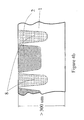
Figure 4a through 4c illustrate sequential steps of a method for fabricating electrodes of a thin wafer photodiode array structure in accordance with the present invention. -
Figure 5 illustrates an exemplary layout of cathode and anode pads across the front surface of the wafer. -
Figure 6 is a cross section taken through one of the metal contacts ofFigure 5 . - The objectives of the embodiments disclosed herein include:
- 1) To provide a multiple element, back side illuminated 2D-photodiode array with a superior performance of all elements;
- 2) To provide a fabrication method for the back side-illuminated photodiode array on an ultra thin wafer.
- It is therefore an obj ect to provide a structure for silicon multi-element, 2-D photodiode arrays having improved characteristics, making it useful in such applications as CT scanner applications, etc.
- Another object is to provide a method of fabricating si devices on ultra thin wafers, which method can be suitable for fabrication of flip-chip, multi-element, 2-dimensional arrays of silicon photodiodes.
- In this disclosure, first preferred embodiments of finished diode arrays will be described, and then the preferred method of fabricating the arrays will be described.
-
Figure 2 is a simplified cross-sectional view of a semiconductor ultra-thin chip photodiode array in accordance with a preferred embodiment. The structure is built using either n-type or p-type bulk silicon 1. For brevity, the anode in the case of p-on-n structure or the cathode in the case of n-on-p structure will be referred to as "the first electrode", while the cathode in the case of p-on-n structure and the anode in the case of n-on-p structure will be referred to as "the second electrode." - The material resistivity, thickness of the wafer/die, dopants concentrations and doses, and diffusion conditions are preferably chosen to satisfy the following requirements:
- a) The active area (the first electrode)
diffusion 2 extends sufficiently close to the back surface of the finished die that the rest of the volume between the diffusion edge and the blanket implant in the die back surface and part of the blanket implant, they space indicated as "d" in theFigure 2 , becomes completely depleted at a zero volt bias; - b) The uniform, "blanket"
type implantation 5 of the back side of the wafer with the implant of the same polarity as the one of the majority carriers of thewafer bulk 1 provides excellent majority carrier conductivity across the wafer back side; and ensures a vertical electric field for carrier collection beneath the first electrode to minimize cross talk; - c) The second electrode,
diffusion 8, is applied from the front surface of the wafer using the implantation and drive protocols that allow for the diffusion to reach the wafer back side, overlapping thereby with theblanket implantation 5 and providing perfect electrical contacts between the second electrode network across the entire wafer. At the same time, anoxide layer 12 is grown on the front surface, shown inFigure 6 , but not shown in the earlier Figures for clarity in the illustrations of the doped regions. - An example of a real structure built using a n-type bulk Si with the resistivity of approximately 400 ohm-cm is shown schematically in
Figure 3 . At a zero bias, the width of a depletion region is approximately 9µm and extends up to and into (but not through) theblanket implantation 5 in the wafer back side. (See the hatched withdots area 9 inFigure 3 . Theblanket diffusion 5 is only approximately 0.6µm thick, so the depletion region extends approximately to, but not quite all the way to, the wafer back side.) The built-in potential creates an electric field across the depletion region and facilitates rapid collection of non-equilibrium carriers created by light near the back surface of the die. The non-equilibrium carriers have no or very little possibility of being collected by the electrodes from adjacent cells because: - The electric field near the die back surface, where the carriers photo-generation predominantly occurs is directed perpendicular to the die surface; therefore, the carriers move (drift) primarily toward the junction of the same cell, having almost no possibility of being trapped by an adjacent cell;
- The second
electrode diffusion region 8, which is n+ diffusion in the case ofFigure 3 , spans the entire thickness of the die and acts as an effective carrier isolator from adjacent cells. - The
first electrode diffusion 2 may overlap with thesecond electrode diffusion 8 close to the front surface of the die as shown inFigure 3 . This overlapping may significantly decrease the breakdown voltage, which is not important for a zero bias device. - Thus, exemplary representative diffusion profiles of the
first electrode 2 andsecond electrode 8 are shown inFigure 3 . The depth of thefirst electrode diffusion 2 should be less than the finished substrate thickness (typically less than 50 µm, and more typically approximately 30 µm as shown inFigure 3 ) by an amount that approximately equals the depletion depth for thesubstrate material 1 at zero bias. Thesecond electrode diffusion 8 should span the entire thickness of the substrate, or at least to a sufficient depth to provide a reliable low resistance contact with theblanket implantation 5 of the back side of the wafer. Note that thedopants - Such a structure may be fabricated starting with a thicker substrate (for example 300 µm) for structural stiffness and integrity during the processing, using three masking steps:
- First, as shown in
Figure 4a , thesecond electrode 8 implantation/diffusion is applied followed by a drive. At this stage, the difference in the final diffusion depths for thefirst electrodes 2 and second electrodes 8 (approximately 9µm) is formed. - Second, as shown in
Figure 4b , thefirst electrode 2 implantation/diffusion is applied followed by a drive. By the end of this stage, thediffusion profiles - Third, as shown in
Figure 4c , thesecond electrode 8 receives an additional enhancement followed by a drive to ensure superior electrical contacts and to activate dopants. At this stage, the profiles of both the cathode and anode diffusions reach their final configurations (see the solid lines and hatched areas inFigure 4c ). The diffusion profiles prior to this third step of dopants implantation/diffusion/drive are shown schematically with the dashed lines inFigure 4c . The future back surface of the wafer after back side grinding and polishing is shown schematically with the dashedline 10. - The array is then reduced in thickness by grinding the back side of the array, preferably to provide a substrate thickness of under approximately 50 µm, and more preferably to approximately 30 µm. The final thickness achieved, of course, is preferably selected in accordance with the resistivity of the substrate and the depth of the first electrode diffusion so that the diffusion is spaced away form the back side of the substrate an amount that approximately equals the depletion depth for the substrate material at zero bias. Then a blanket implant of the first conductivity type is made to the back side of the wafer, which implant improves both the charge collection efficiency and DC/AC electrical performance of the photodiode arrays. Activation of the implant does not significantly alter the first and second electrode diffusions. Alternatively, a diffusion for the back side could be used if desired. The blanket implant is quite thin compared to the depletion region, with the depletion region extending into, but not through, the blanket implant in the final array.
- An ideal flatness of the back side surface of the die is very important for many applications, e.g., for CT scanners that require attaching of a scintillator crystal to the back side of the photodiode array. To help satisfy this requirement, the
oxide layer 12 is evenly patterned and themetal pads 14 contacting thefirst electrode 2 andsecond electrode 8 are evenly spaced across the surface of thedie 16 and made the same size to provide identical ball bumping conditions throughout the wafer (seeFigures 5 and6 ). Theoxide layer 12 andmetal pads 14 are represented by the larger diameter circles inFigure 5 , with the smaller diameter circles describing the contact openings. - The present photodiode arrays exhibit very low cross talk because of the excellent isolation of each pixel. Also, because of the small depletion volume, the arrays exhibit low noise and low temperature sensitivity. When used in X-ray systems, they exhibit low radiation damage, and have thermal characteristics similar to scintillators to which they will are mounted. The technique of using a deep diffusion in conjunction with a thin substrate for making electrical contact to the back side of the substrate may, of course be used in other semiconductor devices. While the deep diffusion in the current invention is of the same conductivity type as the substrate, the deep diffusion may be of the opposite conductivity type in an alternative device, if desired.
- While preferred exemplary embodiments of the present invention have been disclosed herein, such disclosure is only for purposes of understanding the exemplary embodiments and not by way of limitation of the invention. It will be obvious to those skilled in the art that various changes in fabrication process and structure of the photodiode arrays may be made without departing from the scope of the invention defined by the following claims.
Claims (23)
- A back illuminated photodiode array comprising:a substrate (1) of a first conductivity type having first and second surfaces;the second surface having a layer (5) of the first conductivity type having a greater conductivity than the substrate (1);a matrix of regions (8) of the first conductivity type of a higher conductivity than the substrate (1) extending from the first surface of the substrate (1) to the layer (5) of the first conductivity type having a greater conductivity than the substrate (1);a plurality of regions (2) of a second conductivity type interspersed within the matrix of regions (8) of the first conductivity type and not extending to the layer (5) of the first conductivity type; anda plurality of contacts (3,4) on the first surface for making electrical contract with the matrix of regions (8) of the first conductivity type and the plurality of regions (2) of the second conductivity type.
- A photodiode array according to claim I wherein the plurality of regions (2) of the second conductivity type are separated from the second surface of the substrate (1) by an amount that approximately equals the depletion depth for the substrate at zero bias.
- A photodiode array according to claim 1 wherein the plurality of regions (2) of the second conductivity type are separated from the second surface of the substrate (1) by approximately 9 µm.
- A photodiode array according to claim 2 wherein the substrate (1) is an n-type silicon substrate having a resistivity of approximately 400 ohm-cm.
- A photodiode array according to claim 1 wherein the plurality of contacts (3,4) are a plurality of ball grid contacts.
- A photodiode array according to claim 5 wherein the plurality of contacts (3,4) are of substantially equal size evenly distributed the photodiode array.
- A photodiode array according to claim 1 wherein the matrix of regions (8) of a first conductivity type comprises a rectangular matrix defining an X-Y matrix of square regions, each square region containing a respective one of the plurality of regions (2) of the second conductivity type.
- A photodiode array according to claim 7 wherein doping forming the matrix of regions (8) of a first conductivity type and the plurality of regions (2) of the second conductivity type overlap.
- A photodiode array according to claim 1 wherein the substrate (1) has a thickness of less than approximately 50 µm.
- A photodiode array according to claim 1 wherein the substrate (1) has a thickness of approximately 30 µm.
- A photodiode array according to claim 1 wherein the substrate (1) is a silicon substrate.
- A photodiode array according to claim 1 wherein the plurality of regions (2) of the second conductivity type do not extend to the layer of the first conductivity type on the second surface of the substrate.
- A method of fabricating a back-illuminated photodiode array comprising:providing a semiconductor substrate (1) of a first conductivity type;forming a matrix of regions (8) of the first conductivity type of a higher conductivity than the substrate;forming a plurality of regions (2) of a second conductivity type interspersed within the matrix of regions (8) of the first conductivity type;forming a layer (5) of the first conductivity type having a greater conductivity than the substrate on a second surface of the substrate, wherein the matrix of regions (8) and the layer (5) are formed such that the matrix of regions (8) extends from a first surface through the substrate to the layer (5) and the plurality of regions (2) do not extend to the layer (5) of the first conductivity type; andforming a plurality of contacts (3,4) on the first surface for making electrical contact with the matrix of regions (8) of the first conductivity type and the plurality of regions (2) of the second conductivity type.
- A method according to claim 13 wherein the matrix of regions (8) of the first conductivity type extending through the substrate are formed by forming diffusion that are deeper than the plurality of regions of the second conductivity type of the semiconductor device, and grinding the substrate from the second surface to reduce the thickness of the substrate to expose the matrix of regions from the second surface of the substrate.
- A method according to claim 13, wherein:forming the matrix of regions (8) includes a high temperature diffusion,;providing the plurality of regions (2) of the second conductivity type interspersed within the matrix of regions (8) of the first conductivity type, includes an additional high temperature diffusion, the plurality of regions of the second conductivity type (2) extending into the substrate (1) from the first surface a shorter distance than the matrix of regions (8);andforming the matrix of regions (8) of the first conductivity type extending through the substrate comprises grinding the substrate from the second surface to reduce the thickness of the substrate and to expose the matrix of regions of a first conductivity type and not the plurality of regions of the second conductivity type at the second surface of the substrate.
- A method according to claim 13 wherein the layer (5) of the first conductivity type having a conductivity greater than the substrate (1) on the second surface of the substrate is provided by implantation.
- A method according to claim 15 wherein the substrate (1) is ground to a thickness that separates the plurality of regions (2) of the second conductivity type from the second surface of the substrate (1) by an amount that approximately equals the depletion depth for the substrate at zero bias.
- A method according to claim 13 wherein the plurality of regions (2) of the second conductivity type are separated from the second surface of the substrate by approximately 9 µm.
- A method according to claim 13 wherein the substrate (1) provided is an n-type silicon substrate having a resistivity of approximately 400 ohm-cm.
- A method according to claim 13 wherein the plurality of contacts (3,4) are a plurality of ball grid contacts.
- A method according to claim 20 wherein the plurality of contacts (3,4) are of substantially equal size evenly distributed across the photodiode array.
- A method according to claim 15 wherein the substrate (1) is ground to a thickness of less than approximately 50 µm.
- A method according to claim 15 wherein the substrate (1) is ground to a thickness of approximately 30 µm.
Priority Applications (1)
| Application Number | Priority Date | Filing Date | Title |
|---|---|---|---|
| EP10075651A EP2270873A3 (en) | 2003-06-25 | 2004-06-22 | Ultra thin back-illuminated photodiode array structures and fabrication methods |
Applications Claiming Priority (2)
| Application Number | Priority Date | Filing Date | Title |
|---|---|---|---|
| US10/606,053 US6762473B1 (en) | 2003-06-25 | 2003-06-25 | Ultra thin back-illuminated photodiode array structures and fabrication methods |
| PCT/US2004/020835 WO2005001941A2 (en) | 2003-06-25 | 2004-06-22 | Ultra thin back-illuminated photodiode array structures and fabrication methods |
Related Child Applications (1)
| Application Number | Title | Priority Date | Filing Date |
|---|---|---|---|
| EP10075651.9 Division-Into | 2010-10-01 |
Publications (2)
| Publication Number | Publication Date |
|---|---|
| EP1636856A2 EP1636856A2 (en) | 2006-03-22 |
| EP1636856B1 true EP1636856B1 (en) | 2011-10-26 |
Family
ID=32682711
Family Applications (2)
| Application Number | Title | Priority Date | Filing Date |
|---|---|---|---|
| EP10075651A Withdrawn EP2270873A3 (en) | 2003-06-25 | 2004-06-22 | Ultra thin back-illuminated photodiode array structures and fabrication methods |
| EP04777237A Expired - Lifetime EP1636856B1 (en) | 2003-06-25 | 2004-06-22 | Ultra thin back-illuminated photodiode array structures and fabrication methods |
Family Applications Before (1)
| Application Number | Title | Priority Date | Filing Date |
|---|---|---|---|
| EP10075651A Withdrawn EP2270873A3 (en) | 2003-06-25 | 2004-06-22 | Ultra thin back-illuminated photodiode array structures and fabrication methods |
Country Status (7)
| Country | Link |
|---|---|
| US (2) | US6762473B1 (en) |
| EP (2) | EP2270873A3 (en) |
| JP (1) | JP2007521657A (en) |
| CN (1) | CN100533775C (en) |
| AT (1) | ATE531082T1 (en) |
| IL (1) | IL172495A0 (en) |
| WO (1) | WO2005001941A2 (en) |
Families Citing this family (67)
| Publication number | Priority date | Publication date | Assignee | Title |
|---|---|---|---|---|
| US8035183B2 (en) * | 2003-05-05 | 2011-10-11 | Udt Sensors, Inc. | Photodiodes with PN junction on both front and back sides |
| US7709921B2 (en) | 2008-08-27 | 2010-05-04 | Udt Sensors, Inc. | Photodiode and photodiode array with improved performance characteristics |
| US7576369B2 (en) * | 2005-10-25 | 2009-08-18 | Udt Sensors, Inc. | Deep diffused thin photodiodes |
| US7057254B2 (en) | 2003-05-05 | 2006-06-06 | Udt Sensors, Inc. | Front illuminated back side contact thin wafer detectors |
| US7256470B2 (en) * | 2005-03-16 | 2007-08-14 | Udt Sensors, Inc. | Photodiode with controlled current leakage |
| US7656001B2 (en) * | 2006-11-01 | 2010-02-02 | Udt Sensors, Inc. | Front-side illuminated, back-side contact double-sided PN-junction photodiode arrays |
| US8120023B2 (en) * | 2006-06-05 | 2012-02-21 | Udt Sensors, Inc. | Low crosstalk, front-side illuminated, back-side contact photodiode array |
| US8686529B2 (en) | 2010-01-19 | 2014-04-01 | Osi Optoelectronics, Inc. | Wavelength sensitive sensor photodiodes |
| US7880258B2 (en) * | 2003-05-05 | 2011-02-01 | Udt Sensors, Inc. | Thin wafer detectors with improved radiation damage and crosstalk characteristics |
| US8519503B2 (en) * | 2006-06-05 | 2013-08-27 | Osi Optoelectronics, Inc. | High speed backside illuminated, front side contact photodiode array |
| US7279731B1 (en) * | 2006-05-15 | 2007-10-09 | Udt Sensors, Inc. | Edge illuminated photodiodes |
| US7655999B2 (en) | 2006-09-15 | 2010-02-02 | Udt Sensors, Inc. | High density photodiodes |
| US7075091B2 (en) * | 2004-01-29 | 2006-07-11 | Ge Medical Systems Global Technology Company, Llc | Apparatus for detecting ionizing radiation |
| US7439516B2 (en) * | 2004-10-01 | 2008-10-21 | General Electric Company | Module assembly for multiple die back-illuminated diode |
| EP1872396A4 (en) * | 2005-04-22 | 2009-09-23 | Icemos Technology Corp | SUPERJUNCTION DEVICE HAVING OXIDE-COATED TRENCHES AND METHOD OF MANUFACTURING THE SAME |
| US20080099924A1 (en) * | 2005-05-04 | 2008-05-01 | Icemos Technology Corporation | Silicon Wafer Having Through-Wafer Vias With A Predetermined Geometric Shape |
| TW200644165A (en) * | 2005-05-04 | 2006-12-16 | Icemos Technology Corp | Silicon wafer having through-wafer vias |
| US20060289777A1 (en) * | 2005-06-29 | 2006-12-28 | Wen Li | Detector with electrically isolated pixels |
| US7741172B2 (en) * | 2005-08-10 | 2010-06-22 | Icemos Technology Ltd. | Positive-intrinsic-negative (PIN)/negative-intrinsic-positive (NIP) diode |
| US7446018B2 (en) | 2005-08-22 | 2008-11-04 | Icemos Technology Corporation | Bonded-wafer superjunction semiconductor device |
| US7768085B2 (en) * | 2005-10-11 | 2010-08-03 | Icemos Technology Ltd. | Photodetector array using isolation diffusions as crosstalk inhibitors between adjacent photodiodes |
| US7560791B2 (en) * | 2005-10-28 | 2009-07-14 | Icemos Technology Ltd. | Front lit PIN/NIP diode having a continuous anode/cathode |
| US7745798B2 (en) * | 2005-11-15 | 2010-06-29 | Fujifilm Corporation | Dual-phosphor flat panel radiation detector |
| US7576404B2 (en) * | 2005-12-16 | 2009-08-18 | Icemos Technology Ltd. | Backlit photodiode and method of manufacturing a backlit photodiode |
| US7935933B2 (en) * | 2006-01-30 | 2011-05-03 | General Electric Company | Detector for an x-ray imaging system |
| WO2007103255A2 (en) * | 2006-03-02 | 2007-09-13 | Icemos Technology Corporation | Photodiode having increased proportion of light-sensitive area to ligth-insensitive area |
| JP2009528704A (en) * | 2006-03-02 | 2009-08-06 | アイスモス テクノロジー コーポレイション | Front-side electrical contact for photodetector array and method of manufacturing the same |
| US7576371B1 (en) | 2006-03-03 | 2009-08-18 | Array Optronix, Inc. | Structures and methods to improve the crosstalk between adjacent pixels of back-illuminated photodiode arrays |
| US20070241377A1 (en) * | 2006-04-12 | 2007-10-18 | Semicoa | Back-illuminated photo-transistor arrays for computed tomography and other imaging applications |
| ATE500621T1 (en) * | 2006-04-25 | 2011-03-15 | Koninkl Philips Electronics Nv | IMPLEMENTATION OF AVALANCHE PHOTODIODES IN (BI) CMOS PROCESSES |
| US7429772B2 (en) | 2006-04-27 | 2008-09-30 | Icemos Technology Corporation | Technique for stable processing of thin/fragile substrates |
| US7667400B1 (en) | 2006-06-09 | 2010-02-23 | Array Optronix, Inc. | Back-illuminated Si photomultipliers: structure and fabrication methods |
| WO2008021973A2 (en) * | 2006-08-10 | 2008-02-21 | Icemos Technology Corporation | Method of manufacturing a photodiode array with through-wafer vias |
| US20080079108A1 (en) * | 2006-09-29 | 2008-04-03 | Taiwan Semiconductor Manufacturing Company, Ltd. | Method for Improving Sensitivity of Backside Illuminated Image Sensors |
| US8436443B2 (en) | 2006-09-29 | 2013-05-07 | Taiwan Semiconductor Manufacturing Company, Ltd. | Backside depletion for backside illuminated image sensors |
| US9178092B2 (en) | 2006-11-01 | 2015-11-03 | Osi Optoelectronics, Inc. | Front-side illuminated, back-side contact double-sided PN-junction photodiode arrays |
| DE102007007584A1 (en) | 2006-12-29 | 2008-07-03 | Osram Opto Semiconductors Gmbh | Semiconductor detector arrangement for use as back-illuminated multipin-photo detectors or charge coupled devices sensors, has multiple regions of semiconductor substrate spatial assigned to semiconductor structures |
| US7723172B2 (en) | 2007-04-23 | 2010-05-25 | Icemos Technology Ltd. | Methods for manufacturing a trench type semiconductor device having a thermally sensitive refill material |
| US8580651B2 (en) * | 2007-04-23 | 2013-11-12 | Icemos Technology Ltd. | Methods for manufacturing a trench type semiconductor device having a thermally sensitive refill material |
| US7679805B2 (en) * | 2007-07-11 | 2010-03-16 | Cubic Corporation | Flip chip quantum well modulator |
| EP2188840A1 (en) * | 2007-08-10 | 2010-05-26 | Array Optronix, Inc. | Back-illuminated, thin photodiode arrays with trench isolation |
| US20090085148A1 (en) * | 2007-09-28 | 2009-04-02 | Icemos Technology Corporation | Multi-directional trenching of a plurality of dies in manufacturing superjunction devices |
| US20100053802A1 (en) * | 2008-08-27 | 2010-03-04 | Masaki Yamashita | Low Power Disk-Drive Motor Driver |
| US7846821B2 (en) | 2008-02-13 | 2010-12-07 | Icemos Technology Ltd. | Multi-angle rotation for ion implantation of trenches in superjunction devices |
| US8030133B2 (en) * | 2008-03-28 | 2011-10-04 | Icemos Technology Ltd. | Method of fabricating a bonded wafer substrate for use in MEMS structures |
| US7902540B2 (en) * | 2008-05-21 | 2011-03-08 | International Business Machines Corporation | Fast P-I-N photodetector with high responsitivity |
| US20090314947A1 (en) * | 2008-05-30 | 2009-12-24 | Array Optronix, Inc. | Radiation Detector with Isolated Pixels Photosensitive Array for CT and Other Imaging Applications |
| US7851698B2 (en) * | 2008-06-12 | 2010-12-14 | Sunpower Corporation | Trench process and structure for backside contact solar cells with polysilicon doped regions |
| GB2476019B (en) * | 2008-09-15 | 2013-03-13 | Osi Optoelectronics Inc | Thin active layer fishbone photodiode with a shallow N+ layer and method of manufacturing the same |
| US20100108893A1 (en) * | 2008-11-04 | 2010-05-06 | Array Optronix, Inc. | Devices and Methods for Ultra Thin Photodiode Arrays on Bonded Supports |
| US8399909B2 (en) * | 2009-05-12 | 2013-03-19 | Osi Optoelectronics, Inc. | Tetra-lateral position sensing detector |
| US8409908B2 (en) * | 2009-07-30 | 2013-04-02 | General Electric Company | Apparatus for reducing photodiode thermal gain coefficient and method of making same |
| US8614495B2 (en) | 2010-04-23 | 2013-12-24 | Taiwan Semiconductor Manufacturing Company, Ltd. | Back side defect reduction for back side illuminated image sensor |
| DE102011009373B4 (en) * | 2011-01-25 | 2017-08-03 | Austriamicrosystems Ag | Photodiode device |
| US8598021B2 (en) * | 2011-09-29 | 2013-12-03 | Varian Semiconductor Equipment Associates, Inc. | Method for junction avoidance on edge of workpieces |
| US8822262B2 (en) | 2011-12-22 | 2014-09-02 | Sunpower Corporation | Fabricating solar cells with silicon nanoparticles |
| US8946814B2 (en) | 2012-04-05 | 2015-02-03 | Icemos Technology Ltd. | Superjunction devices having narrow surface layout of terminal structures, buried contact regions and trench gates |
| US9318524B2 (en) | 2012-04-30 | 2016-04-19 | Koninklijke Philips N.V. | Imaging detector with per pixel analog channel well isolation with decoupling |
| JP6084401B2 (en) * | 2012-08-30 | 2017-02-22 | 浜松ホトニクス株式会社 | Method for manufacturing side-incident photodiodes |
| US9576842B2 (en) | 2012-12-10 | 2017-02-21 | Icemos Technology, Ltd. | Grass removal in patterned cavity etching |
| JP6231741B2 (en) | 2012-12-10 | 2017-11-15 | キヤノン株式会社 | Solid-state imaging device and manufacturing method thereof |
| US8912615B2 (en) | 2013-01-24 | 2014-12-16 | Osi Optoelectronics, Inc. | Shallow junction photodiode for detecting short wavelength light |
| US10050076B2 (en) * | 2014-10-07 | 2018-08-14 | Terapede Systems Inc. | 3D high resolution X-ray sensor with integrated scintillator grid |
| JP6570417B2 (en) * | 2014-10-24 | 2019-09-04 | 株式会社半導体エネルギー研究所 | Imaging apparatus and electronic apparatus |
| JP6736351B2 (en) * | 2015-06-19 | 2020-08-05 | 株式会社半導体エネルギー研究所 | Semiconductor device |
| JP6986831B2 (en) * | 2015-07-17 | 2021-12-22 | 株式会社半導体エネルギー研究所 | Semiconductor devices and electronic devices |
| US9930281B2 (en) | 2016-01-20 | 2018-03-27 | Semiconductor Components Industries, Llc | Image sensors having photodiode regions implanted from multiple sides of a substrate |
Citations (2)
| Publication number | Priority date | Publication date | Assignee | Title |
|---|---|---|---|---|
| US5670383A (en) * | 1994-04-04 | 1997-09-23 | General Electric Company | Method for fabrication of deep-diffused avalanche photodiode |
| US20020011639A1 (en) * | 1999-07-02 | 2002-01-31 | Carlson Lars S. | Indirect back surface contact to semiconductor devices |
Family Cites Families (21)
| Publication number | Priority date | Publication date | Assignee | Title |
|---|---|---|---|---|
| US3574009A (en) * | 1968-03-06 | 1971-04-06 | Unitrode Corp | Controlled doping of semiconductors |
| GB1553356A (en) * | 1976-12-27 | 1979-09-26 | Hamasawa Kogyo Kk | Solar battery |
| US5072312A (en) * | 1988-03-15 | 1991-12-10 | Siemens Aktiengesellschaft | Thyristor with high positive and negative blocking capability |
| FR2640082B1 (en) * | 1988-12-07 | 1991-03-29 | Telemecanique | SYMMETRIC POWER SEMICONDUCTOR DEVICE AND MANUFACTURING METHOD THEREOF |
| JPH02237154A (en) * | 1989-03-10 | 1990-09-19 | Mitsubishi Electric Corp | Light-detecting device |
| JP2557750B2 (en) * | 1991-02-27 | 1996-11-27 | 三洋電機株式会社 | Optical semiconductor device |
| CA2070708C (en) * | 1991-08-08 | 1997-04-29 | Ichiro Kasai | Visible and infrared indium antimonide (insb) photodetector with non-flashing light receiving surface |
| US5538564A (en) * | 1994-03-18 | 1996-07-23 | Regents Of The University Of California | Three dimensional amorphous silicon/microcrystalline silicon solar cells |
| DE69637636D1 (en) * | 1995-12-06 | 2008-09-25 | Sony Corp | Semiconductor device consisting of a photodiode and a bipolar element, and method of manufacturing |
| JP2882354B2 (en) * | 1996-04-30 | 1999-04-12 | 日本電気株式会社 | Integrated circuit device with built-in light receiving element |
| JPH09321265A (en) * | 1996-05-31 | 1997-12-12 | Sony Corp | Semiconductor device |
| JP3924352B2 (en) * | 1997-06-05 | 2007-06-06 | 浜松ホトニクス株式会社 | Backside illuminated light receiving device |
| US6111305A (en) * | 1997-10-09 | 2000-08-29 | Nippon Telegraph And Telephone Corporation | P-I-N semiconductor photodetector |
| US6727521B2 (en) * | 2000-09-25 | 2004-04-27 | Foveon, Inc. | Vertical color filter detector group and array |
| US6545331B1 (en) * | 1999-12-10 | 2003-04-08 | Innotech Corporation | Solid state imaging device, manufacturing method thereof, and solid state imaging apparatus |
| US20020020846A1 (en) * | 2000-04-20 | 2002-02-21 | Bo Pi | Backside illuminated photodiode array |
| US6426991B1 (en) * | 2000-11-16 | 2002-07-30 | Koninklijke Philips Electronics N.V. | Back-illuminated photodiodes for computed tomography detectors |
| US6713768B2 (en) * | 2001-04-16 | 2004-03-30 | Photon Imaging, Inc. | Junction-side illuminated silicon detector arrays |
| US6933489B2 (en) * | 2002-05-10 | 2005-08-23 | Hamamatsu Photonics K.K. | Back illuminated photodiode array and method of manufacturing the same |
| KR101019807B1 (en) * | 2002-08-09 | 2011-03-04 | 하마마츠 포토닉스 가부시키가이샤 | Photodiode Arrays, Manufacturing Methods thereof, and Radiation Detectors |
| US6853046B2 (en) * | 2002-09-24 | 2005-02-08 | Hamamatsu Photonics, K.K. | Photodiode array and method of making the same |
-
2003
- 2003-06-25 US US10/606,053 patent/US6762473B1/en not_active Expired - Fee Related
-
2004
- 2004-06-08 US US10/863,558 patent/US7112465B2/en not_active Expired - Fee Related
- 2004-06-22 WO PCT/US2004/020835 patent/WO2005001941A2/en not_active Ceased
- 2004-06-22 JP JP2006517765A patent/JP2007521657A/en active Pending
- 2004-06-22 AT AT04777237T patent/ATE531082T1/en not_active IP Right Cessation
- 2004-06-22 EP EP10075651A patent/EP2270873A3/en not_active Withdrawn
- 2004-06-22 CN CNB2004800247278A patent/CN100533775C/en not_active Expired - Fee Related
- 2004-06-22 EP EP04777237A patent/EP1636856B1/en not_active Expired - Lifetime
-
2005
- 2005-12-11 IL IL172495A patent/IL172495A0/en unknown
Patent Citations (2)
| Publication number | Priority date | Publication date | Assignee | Title |
|---|---|---|---|---|
| US5670383A (en) * | 1994-04-04 | 1997-09-23 | General Electric Company | Method for fabrication of deep-diffused avalanche photodiode |
| US20020011639A1 (en) * | 1999-07-02 | 2002-01-31 | Carlson Lars S. | Indirect back surface contact to semiconductor devices |
Also Published As
| Publication number | Publication date |
|---|---|
| IL172495A0 (en) | 2006-04-10 |
| EP2270873A2 (en) | 2011-01-05 |
| JP2007521657A (en) | 2007-08-02 |
| US20040262652A1 (en) | 2004-12-30 |
| US6762473B1 (en) | 2004-07-13 |
| CN100533775C (en) | 2009-08-26 |
| ATE531082T1 (en) | 2011-11-15 |
| CN1842921A (en) | 2006-10-04 |
| EP1636856A2 (en) | 2006-03-22 |
| WO2005001941A3 (en) | 2005-03-10 |
| EP2270873A3 (en) | 2012-03-28 |
| US7112465B2 (en) | 2006-09-26 |
| WO2005001941A2 (en) | 2005-01-06 |
Similar Documents
| Publication | Publication Date | Title |
|---|---|---|
| US7112465B2 (en) | Fabrication methods for ultra thin back-illuminated photodiode array | |
| US7462553B2 (en) | Ultra thin back-illuminated photodiode array fabrication methods | |
| US7875890B1 (en) | Structures and methods to improve the crosstalk between adjacent pixels of back-illuminated photodiode arrays | |
| CN110957335B (en) | CMOS image sensor and method for forming image sensor | |
| US20210091125A1 (en) | Image sensor with a high absorption layer | |
| EP3309846A1 (en) | Avalanche diode and method for manufacturing the same | |
| US20100108893A1 (en) | Devices and Methods for Ultra Thin Photodiode Arrays on Bonded Supports | |
| US20100301442A1 (en) | Optical semiconductor device | |
| US20090239328A1 (en) | Photo-detector for detecting image signal of infrared laser radar and method of manufacturing the same | |
| WO2008143413A1 (en) | Phototransistor having a buried collector | |
| US7968358B2 (en) | Digital radiographic flat-panel imaging array with dual height semiconductor and method of making same | |
| US20260040718A1 (en) | Single-photon detector and manufacturing method therefor | |
| CN117116957A (en) | Single-photon avalanche diode array and preparation method thereof | |
| CN111279493B (en) | Integrated sensor for ionizing radiation and ionizing particles | |
| US8766339B2 (en) | Highly efficient CMOS technology compatible silicon photoelectric multiplier | |
| DE102018122505B4 (en) | Backside deep trench insulating (BDTI) structure for image sensor with pinned photodiode | |
| CN111628033A (en) | Manufacturing method of photodetector | |
| WO2024185302A1 (en) | Light detection device | |
| KR102759280B1 (en) | Avalanche type photodetector (modified) and its manufacturing method (modified) | |
| EP1833095A1 (en) | Photo diode having reduced dark current | |
| CN119384049B (en) | Back-illuminated photodiode structure and fabrication method, X-ray detector | |
| EP4369421A1 (en) | Light-receiving device, x-ray imaging device, and electronic equipment | |
| KR20230021300A (en) | Spad pixel structure of backside illuminated image sensor | |
| JPH10200145A (en) | Photoelectric conversion device |
Legal Events
| Date | Code | Title | Description |
|---|---|---|---|
| PUAI | Public reference made under article 153(3) epc to a published international application that has entered the european phase |
Free format text: ORIGINAL CODE: 0009012 |
|
| 17P | Request for examination filed |
Effective date: 20051219 |
|
| AK | Designated contracting states |
Kind code of ref document: A2 Designated state(s): AT BE BG CH CY CZ DE DK EE ES FI FR GB GR HU IE IT LI LU MC NL PL PT RO SE SI SK TR |
|
| RIN1 | Information on inventor provided before grant (corrected) |
Inventor name: HICKS, CHRIS Inventor name: BARTLEY, EDDIE Inventor name: GOUSHCHA, ALEXANDER, O. Inventor name: KALATSKY, MARK Inventor name: METZLER, RICHARD, A. Inventor name: TULBURE, DAN |
|
| DAX | Request for extension of the european patent (deleted) | ||
| RAP1 | Party data changed (applicant data changed or rights of an application transferred) |
Owner name: ARRAY OPTRONIX, INC. |
|
| GRAP | Despatch of communication of intention to grant a patent |
Free format text: ORIGINAL CODE: EPIDOSNIGR1 |
|
| GRAS | Grant fee paid |
Free format text: ORIGINAL CODE: EPIDOSNIGR3 |
|
| GRAA | (expected) grant |
Free format text: ORIGINAL CODE: 0009210 |
|
| AK | Designated contracting states |
Kind code of ref document: B1 Designated state(s): AT BE BG CH CY CZ DE DK EE ES FI FR GB GR HU IE IT LI LU MC NL PL PT RO SE SI SK TR |
|
| REG | Reference to a national code |
Ref country code: GB Ref legal event code: FG4D |
|
| REG | Reference to a national code |
Ref country code: CH Ref legal event code: EP |
|
| REG | Reference to a national code |
Ref country code: IE Ref legal event code: FG4D |
|
| REG | Reference to a national code |
Ref country code: DE Ref legal event code: R096 Ref document number: 602004035042 Country of ref document: DE Effective date: 20111222 |
|
| REG | Reference to a national code |
Ref country code: NL Ref legal event code: T3 |
|
| REG | Reference to a national code |
Ref country code: AT Ref legal event code: MK05 Ref document number: 531082 Country of ref document: AT Kind code of ref document: T Effective date: 20111026 |
|
| PG25 | Lapsed in a contracting state [announced via postgrant information from national office to epo] |
Ref country code: BE Free format text: LAPSE BECAUSE OF FAILURE TO SUBMIT A TRANSLATION OF THE DESCRIPTION OR TO PAY THE FEE WITHIN THE PRESCRIBED TIME-LIMIT Effective date: 20111026 |
|
| PG25 | Lapsed in a contracting state [announced via postgrant information from national office to epo] |
Ref country code: PT Free format text: LAPSE BECAUSE OF FAILURE TO SUBMIT A TRANSLATION OF THE DESCRIPTION OR TO PAY THE FEE WITHIN THE PRESCRIBED TIME-LIMIT Effective date: 20120227 Ref country code: PL Free format text: LAPSE BECAUSE OF FAILURE TO SUBMIT A TRANSLATION OF THE DESCRIPTION OR TO PAY THE FEE WITHIN THE PRESCRIBED TIME-LIMIT Effective date: 20111026 Ref country code: SE Free format text: LAPSE BECAUSE OF FAILURE TO SUBMIT A TRANSLATION OF THE DESCRIPTION OR TO PAY THE FEE WITHIN THE PRESCRIBED TIME-LIMIT Effective date: 20111026 Ref country code: GR Free format text: LAPSE BECAUSE OF FAILURE TO SUBMIT A TRANSLATION OF THE DESCRIPTION OR TO PAY THE FEE WITHIN THE PRESCRIBED TIME-LIMIT Effective date: 20120127 Ref country code: SI Free format text: LAPSE BECAUSE OF FAILURE TO SUBMIT A TRANSLATION OF THE DESCRIPTION OR TO PAY THE FEE WITHIN THE PRESCRIBED TIME-LIMIT Effective date: 20111026 |
|
| PG25 | Lapsed in a contracting state [announced via postgrant information from national office to epo] |
Ref country code: CY Free format text: LAPSE BECAUSE OF FAILURE TO SUBMIT A TRANSLATION OF THE DESCRIPTION OR TO PAY THE FEE WITHIN THE PRESCRIBED TIME-LIMIT Effective date: 20111026 |
|
| PG25 | Lapsed in a contracting state [announced via postgrant information from national office to epo] |
Ref country code: EE Free format text: LAPSE BECAUSE OF FAILURE TO SUBMIT A TRANSLATION OF THE DESCRIPTION OR TO PAY THE FEE WITHIN THE PRESCRIBED TIME-LIMIT Effective date: 20111026 Ref country code: SK Free format text: LAPSE BECAUSE OF FAILURE TO SUBMIT A TRANSLATION OF THE DESCRIPTION OR TO PAY THE FEE WITHIN THE PRESCRIBED TIME-LIMIT Effective date: 20111026 Ref country code: CZ Free format text: LAPSE BECAUSE OF FAILURE TO SUBMIT A TRANSLATION OF THE DESCRIPTION OR TO PAY THE FEE WITHIN THE PRESCRIBED TIME-LIMIT Effective date: 20111026 Ref country code: BG Free format text: LAPSE BECAUSE OF FAILURE TO SUBMIT A TRANSLATION OF THE DESCRIPTION OR TO PAY THE FEE WITHIN THE PRESCRIBED TIME-LIMIT Effective date: 20120126 Ref country code: DK Free format text: LAPSE BECAUSE OF FAILURE TO SUBMIT A TRANSLATION OF THE DESCRIPTION OR TO PAY THE FEE WITHIN THE PRESCRIBED TIME-LIMIT Effective date: 20111026 |
|
| PG25 | Lapsed in a contracting state [announced via postgrant information from national office to epo] |
Ref country code: IT Free format text: LAPSE BECAUSE OF FAILURE TO SUBMIT A TRANSLATION OF THE DESCRIPTION OR TO PAY THE FEE WITHIN THE PRESCRIBED TIME-LIMIT Effective date: 20111026 Ref country code: RO Free format text: LAPSE BECAUSE OF FAILURE TO SUBMIT A TRANSLATION OF THE DESCRIPTION OR TO PAY THE FEE WITHIN THE PRESCRIBED TIME-LIMIT Effective date: 20111026 |
|
| PLBE | No opposition filed within time limit |
Free format text: ORIGINAL CODE: 0009261 |
|
| STAA | Information on the status of an ep patent application or granted ep patent |
Free format text: STATUS: NO OPPOSITION FILED WITHIN TIME LIMIT |
|
| 26N | No opposition filed |
Effective date: 20120727 |
|
| REG | Reference to a national code |
Ref country code: DE Ref legal event code: R097 Ref document number: 602004035042 Country of ref document: DE Effective date: 20120727 |
|
| REG | Reference to a national code |
Ref country code: NL Ref legal event code: V1 Effective date: 20130101 |
|
| PG25 | Lapsed in a contracting state [announced via postgrant information from national office to epo] |
Ref country code: AT Free format text: LAPSE BECAUSE OF FAILURE TO SUBMIT A TRANSLATION OF THE DESCRIPTION OR TO PAY THE FEE WITHIN THE PRESCRIBED TIME-LIMIT Effective date: 20111026 Ref country code: MC Free format text: LAPSE BECAUSE OF NON-PAYMENT OF DUE FEES Effective date: 20120630 |
|
| REG | Reference to a national code |
Ref country code: CH Ref legal event code: PL |
|
| REG | Reference to a national code |
Ref country code: CH Ref legal event code: PL |
|
| GBPC | Gb: european patent ceased through non-payment of renewal fee |
Effective date: 20120622 |
|
| REG | Reference to a national code |
Ref country code: IE Ref legal event code: MM4A |
|
| REG | Reference to a national code |
Ref country code: FR Ref legal event code: ST Effective date: 20130228 |
|
| REG | Reference to a national code |
Ref country code: DE Ref legal event code: R119 Ref document number: 602004035042 Country of ref document: DE Effective date: 20130101 |
|
| PG25 | Lapsed in a contracting state [announced via postgrant information from national office to epo] |
Ref country code: GB Free format text: LAPSE BECAUSE OF NON-PAYMENT OF DUE FEES Effective date: 20120622 Ref country code: LI Free format text: LAPSE BECAUSE OF NON-PAYMENT OF DUE FEES Effective date: 20120630 Ref country code: NL Free format text: LAPSE BECAUSE OF NON-PAYMENT OF DUE FEES Effective date: 20130101 Ref country code: IE Free format text: LAPSE BECAUSE OF NON-PAYMENT OF DUE FEES Effective date: 20120622 Ref country code: ES Free format text: LAPSE BECAUSE OF FAILURE TO SUBMIT A TRANSLATION OF THE DESCRIPTION OR TO PAY THE FEE WITHIN THE PRESCRIBED TIME-LIMIT Effective date: 20120206 Ref country code: FR Free format text: LAPSE BECAUSE OF NON-PAYMENT OF DUE FEES Effective date: 20120702 Ref country code: DE Free format text: LAPSE BECAUSE OF NON-PAYMENT OF DUE FEES Effective date: 20130101 Ref country code: CH Free format text: LAPSE BECAUSE OF NON-PAYMENT OF DUE FEES Effective date: 20120630 |
|
| PG25 | Lapsed in a contracting state [announced via postgrant information from national office to epo] |
Ref country code: FI Free format text: LAPSE BECAUSE OF FAILURE TO SUBMIT A TRANSLATION OF THE DESCRIPTION OR TO PAY THE FEE WITHIN THE PRESCRIBED TIME-LIMIT Effective date: 20111026 |
|
| PG25 | Lapsed in a contracting state [announced via postgrant information from national office to epo] |
Ref country code: TR Free format text: LAPSE BECAUSE OF FAILURE TO SUBMIT A TRANSLATION OF THE DESCRIPTION OR TO PAY THE FEE WITHIN THE PRESCRIBED TIME-LIMIT Effective date: 20111026 |
|
| PG25 | Lapsed in a contracting state [announced via postgrant information from national office to epo] |
Ref country code: LU Free format text: LAPSE BECAUSE OF NON-PAYMENT OF DUE FEES Effective date: 20120622 |
|
| PG25 | Lapsed in a contracting state [announced via postgrant information from national office to epo] |
Ref country code: HU Free format text: LAPSE BECAUSE OF FAILURE TO SUBMIT A TRANSLATION OF THE DESCRIPTION OR TO PAY THE FEE WITHIN THE PRESCRIBED TIME-LIMIT Effective date: 20040622 |