EP1635386A1 - Method of removing molding residues from lead-frames - Google Patents
Method of removing molding residues from lead-frames Download PDFInfo
- Publication number
- EP1635386A1 EP1635386A1 EP04104349A EP04104349A EP1635386A1 EP 1635386 A1 EP1635386 A1 EP 1635386A1 EP 04104349 A EP04104349 A EP 04104349A EP 04104349 A EP04104349 A EP 04104349A EP 1635386 A1 EP1635386 A1 EP 1635386A1
- Authority
- EP
- European Patent Office
- Prior art keywords
- lead
- frame
- frozen
- frozen pellets
- pellets
- Prior art date
- Legal status (The legal status is an assumption and is not a legal conclusion. Google has not performed a legal analysis and makes no representation as to the accuracy of the status listed.)
- Withdrawn
Links
Images

Classifications
-
- H—ELECTRICITY
- H10—SEMICONDUCTOR DEVICES; ELECTRIC SOLID-STATE DEVICES NOT OTHERWISE PROVIDED FOR
- H10W—GENERIC PACKAGES, INTERCONNECTIONS, CONNECTORS OR OTHER CONSTRUCTIONAL DETAILS OF DEVICES COVERED BY CLASS H10
- H10W70/00—Package substrates; Interposers; Redistribution layers [RDL]
- H10W70/01—Manufacture or treatment
- H10W70/04—Manufacture or treatment of leadframes
- H10W70/045—Cleaning
-
- H—ELECTRICITY
- H10—SEMICONDUCTOR DEVICES; ELECTRIC SOLID-STATE DEVICES NOT OTHERWISE PROVIDED FOR
- H10W—GENERIC PACKAGES, INTERCONNECTIONS, CONNECTORS OR OTHER CONSTRUCTIONAL DETAILS OF DEVICES COVERED BY CLASS H10
- H10W72/00—Interconnections or connectors in packages
- H10W72/50—Bond wires
- H10W72/551—Materials of bond wires
- H10W72/552—Materials of bond wires comprising metals or metalloids, e.g. silver
- H10W72/5522—Materials of bond wires comprising metals or metalloids, e.g. silver comprising gold [Au]
-
- H—ELECTRICITY
- H10—SEMICONDUCTOR DEVICES; ELECTRIC SOLID-STATE DEVICES NOT OTHERWISE PROVIDED FOR
- H10W—GENERIC PACKAGES, INTERCONNECTIONS, CONNECTORS OR OTHER CONSTRUCTIONAL DETAILS OF DEVICES COVERED BY CLASS H10
- H10W72/00—Interconnections or connectors in packages
- H10W72/851—Dispositions of multiple connectors or interconnections
- H10W72/874—On different surfaces
- H10W72/884—Die-attach connectors and bond wires
-
- H—ELECTRICITY
- H10—SEMICONDUCTOR DEVICES; ELECTRIC SOLID-STATE DEVICES NOT OTHERWISE PROVIDED FOR
- H10W—GENERIC PACKAGES, INTERCONNECTIONS, CONNECTORS OR OTHER CONSTRUCTIONAL DETAILS OF DEVICES COVERED BY CLASS H10
- H10W90/00—Package configurations
- H10W90/701—Package configurations characterised by the relative positions of pads or connectors relative to package parts
- H10W90/731—Package configurations characterised by the relative positions of pads or connectors relative to package parts of die-attach connectors
- H10W90/736—Package configurations characterised by the relative positions of pads or connectors relative to package parts of die-attach connectors between a chip and a stacked lead frame, conducting package substrate or heat sink
-
- H—ELECTRICITY
- H10—SEMICONDUCTOR DEVICES; ELECTRIC SOLID-STATE DEVICES NOT OTHERWISE PROVIDED FOR
- H10W—GENERIC PACKAGES, INTERCONNECTIONS, CONNECTORS OR OTHER CONSTRUCTIONAL DETAILS OF DEVICES COVERED BY CLASS H10
- H10W90/00—Package configurations
- H10W90/701—Package configurations characterised by the relative positions of pads or connectors relative to package parts
- H10W90/751—Package configurations characterised by the relative positions of pads or connectors relative to package parts of bond wires
- H10W90/756—Package configurations characterised by the relative positions of pads or connectors relative to package parts of bond wires between a chip and a stacked lead frame, conducting package substrate or heat sink
Definitions
- the present invention relates to package manufacturing processes for electronic devices. Particularly, the present invention relates to a process for removing manufacturing molding residues from lead-frames for electronic device packages.
- An electronic device generally includes a circuit that is integrated on a chip of semiconductor material, requiring for its utilization to be housed in a package.
- the package consists of an insulating body, molded over the chip for protecting it, and, typically, of multiple leads projecting from the insulating body to connect the chip to external circuitries, the leads being in turn connected to the chip by means of tiny wires, e.g. of gold.
- the package further includes a paddle onto which the chip is mounted, for holding the chip during subsequent manufacturing stages.
- the packaged electronic devices in most of applications are mounted onto a Printed Circuit Board (shortly, PCB) and the leads are soldered to conductive strips of the PCB to be electrically connected thereto.
- the paddle has a surface that is exposed with respect to the insulating body (such as the so-called exposed-pad packages). In this case, the paddle acts as a heat dissipator, which is soldered in contact with the PCB.
- the lead-frame consists of a support frame structure, from which the leads project, being connected to a plurality of die paddles by means of interconnection bars (that support the die paddles during the package manufacturing process).
- Ni/Pd/Au pre-plated lead-frames copper lead-frames treated with exterior coating of less oxidizable metals compatible with existing technology, such as nickel (Ni), palladium (Pd) and gold (Au), have been developed (Ni/Pd/Au pre-plated lead-frames).
- Palladium plating film has good gold wire bondability and solderability, so it is suitable for IC lead-frames.
- the Pd-plated lead-frame needs a nickel plating underlayer to maintain high joint strength of soldering parts; for example, the nickel layer is of the order of one micrometer and approximately 0.1 ⁇ m of palladium is plated thereon.
- the Pd-plated lead-frame is expected to be more likely stable against heat when further plated with an ultra-thin layer (tens of angstroms) of gold on Pd-film surface.
- the insulating body, wherein the electronic device is embedded is produced by a molding process of a plastic material, which can cause flashes and bleeds over the metal surface of the leads and of the exposed paddle (when exposed from the insulating body).
- Such molding residues on the lead-frame can impair the planarity of the surface of the electronic device that has to be soldered, for example, to the PCB; furthermore, the solderability of the leads and of the die paddle of the electronic device can be greatly reduced.
- the heat dissipation capability of the die paddle and the electrical properties of the leads are impaired.
- solutions known in the art for removing the molding residues from the lead-frames propose different types of processes, such as mechanical or chemical/electro-chemical process, or also processes exploiting lasers.
- mechanical processes consist of a blasting in which solid particles, such as particles of sand, of brass, or other powders, are accelerated to hit the surface of the lead-frames.
- solid particles such as particles of sand, of brass, or other powders
- water jets can be exploited.
- a method of removing molding residues is provided as set forth in the appended claim 1.
- a method of packaging electronic devices is also encompassed.
- an apparatus as set forth in the appended claim 9, is further provided.
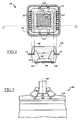
- Fig. 1 illustrates partial bottom plan and sectional elevated side views of a lead-frame 100, onto which electronic circuits integrated in chips 105 of semiconductor material are mounted. Particularly, the lead-frame 100 is exploited for obtaining leaded packages for electronic devices 108, e.g. to be mounted onto a PCB.
- the lead-frame 100 is produced from a conductive plate, typically, a metal plate, such as a copper plate, having a thickness, for example, of the order of few millimeters.
- the lead-frame 100 mainly includes a support frame structure 110 and die mounting paddles 115 (only one shown in the drawing) formed in the metal plate.
- the paddle 115 having roughly a square shape, primarily serves to mechanically hold one or more chips 105 on its upper surface 130 during a package manufacturing process, the paddle 115 in turn being connected to the support frame 110 by means of a plurality of interconnection bars 120.
- the lead-frame 100 further includes a plurality of leads 125 for each paddle 115; the leads 125 project from respective portions of the support frame 110 facing, for example, two opposite sides of the paddle 115.
- the lead-frame 100 is plated with additional metal layers in order to improve the solderability and the wire bondability.
- the lead-frame 100 is firstly plated with nickel, obtaining a layer with thickness of, e.g., hundreds of nanometers.
- a layer of a precious metal, such as palladium, of about tens of nanometers covers the nickel layer.
- the lead-frame 100 is plated with a further precious metal, such as gold; typically, the gold layer is very thin, e.g. in the range of 30 - 150 angstroms.
- the packaged electronic device 108 includes the chip 105, mounted onto the upper surface 130 of the paddle 115, the chip 105 being electrically connected to proximal ends of the corresponding leads 125 by means of tiny metal wires 135 (typically, made of gold).
- the leads 125 are in turn connectable to external circuitries.
- a plane of the paddles 115 is spaced apart from a plane of the leads 125.
- Such a downsetting of the paddle 115 with respect to the leads 125 allows achieving a better looping of the wires 135.
- a deep downsetting of the paddle 115 allows maintaining its lower surface 140 (opposite the upper surface 130 onto which the chip 105 is mounted) exposed from an insulating body 145 of the packaged electronic device 108.
- the insulating body 145 (made of a plastic material, such as an epoxy resin) protects the chip 105 and the wires 135.
- the insulating body 145 also embeds (in addition to the chip 105 and the wires 135) an internal portion of the leads 125 (whereto the wires 135 are connected) and a portion of the interconnection bars 120 extending from the paddle 115. Conversely, an active portion of the leads 125 extending from the support frame 110 of the lead-frame 100 is maintained outside the insulating body 145.
- the packaged electronic device 108 is mounted onto a PCB, which consists of an insulating substrate on which conductive strips are patterned.
- a PCB which consists of an insulating substrate on which conductive strips are patterned.
- the exposed surface 140 of the paddle 115 is soldered onto the PCB and the leads 125 is mechanically and electrically connected to the desired conductive strips of the PCB.
- the paddle 115 in contact with the PCB improves the heat dissipation during the electronic device 108 operation by forming a heat flow path between the chip 105 and the PCB (the paddle 115 acts as a heat dissipator).
- the paddle 115 can be connected to ground, thus reducing loop inductance for high-frequency applications; in such applications the paddle 115 is called "exposed pad".
- the lead-frame 100 is produced by dieing (or also by etching) the metal plate, so as to define the support frame 110, the paddles 115, the interconnection bars 120 and the leads 125. Before assembling chips 105 on its surface, the lead-frame 100 is pre-plated with additional metal layers, as described above, so as to obtain, for example, three additional relatively thin layers of nickel, palladium and gold.
- one or more chips 105 are mounted onto each paddle 115 of the lead-frame 100 and fixed thereto by means of a binding material (such as an adhesive compound). The chip 105 is then connected to the corresponding leads 125 through the gold wires 135.
- a binding material such as an adhesive compound
- the complex of the chip 105 and of the wires 135 is embedded into the insulating body 145, made of an epoxy resin, by means of a molding process, the lower surface 140 of the paddle 115 as well as the active portion of the leads 125 being kept exposed.
- high temperature and pressure liquefies the epoxy resin, which is then forced through a mould chase into a cavity over the chips 105 mounted onto the lead-frame 100.
- the epoxy resin once hardened, forms the body of the final package.
- the packaged electronic devices thus obtained are then separated from each other and from the support frame 110 of the lead-frame 100 by cropping the portions of the interconnection bars 120 projecting from the insulating body 145 and the end portions of the leads 125 connected to the support frame 110.
- residues 150 of epoxy resin such as flashes or bleeds, inevitably form on the exposed surface 140 of the paddle 115 and on the active portion of the leads 125.
- the molding residues 150 cause a reduction of the heat dissipation capability of the paddle 115, as well as a reduction of the solderability, because of an impaired planarity and a decreased area adapted to be placed directly in contact with, e.g., the PCB.
- the molding residues 150 impair the electrical properties of the leads 125 and of the paddle 115, when exploited as an exposed pad.
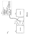
- FIG. 2A a portion of the assembly automated line 200 for the package manufacturing process is schematically illustrated, in which a deflashing process according to an embodiment of the present invention is applied.
- a deflashing process is performed for removing the molding residues (i.e., residues of the molding process) from the lead-frame 100.
- the deflashing process includes a blasting in which suitable pellets are projected against the lead-frame surface to be cleaned.
- the automated line 200 includes a cryogenic apparatus 215 adapted to produce pellets of a frozen substance, preferably but not limitatively dry ice (e.g., solid carbon dioxide, CO 2 ) pellets and to project such pellets against the lead-frame.
- dry ice is frozen carbon dioxide obtained by solidification at temperature of about - 78.5°C; solid carbon dioxide is called "dry ice" since, in normal atmospheric conditions, it changes directly from a solid phase to a gaseous phase (i.e., it sublimates) without passing through a liquid phase.
- the cryogenic apparatus 215 includes a dry ice generator 220, in which dry ice is produced, for example in the form of roughly cylindrical dry ice elements having diameter of the order of few millimeters (for example, of about 2 mm).
- the dry ice cylindrical elements are provided by the dry ice generator 220 to a pellet flow generator 225 (such as the Cryos Cryojet BG 01 model) receiving also dried compressed air from a compressor 230.
- the pellet flow generator 225 is adapted to regulate the injection pressure of the compressed air (for example, between 2 and 15 bar), and for this purpose the pellet flow generator 225 is provided with a suitable regulation knob 231.
- the pellet flow generator 225 exploits the propelling force of the compressed air 245 for projecting the received cylindrical dry ice elements 250 against an internal grid 255, acting as a sieve, with, e.g., square passages having size in a range from approximately 0.5 mm to 2 mm, and preferably in a range from approximately 0.6 mm to 1.4 mm.
- the pellet flow generator 225 generates a flow 260 of dry ice pellets having a size depending of the size of the grid passages (e.g., approximately of 0.8 mm), accelerated by the compressed air 245.
- the size of the dry ice pellets is limited not to have an excessive mass, and thus an excessive momentum when accelerated, in such a way not to cause bendings of the leads.
- the pellet flow generator 225 is preferably provided with two further regulation knobs 232 and 233 for regulating a carrying pressure of the compressed air (for example, between approximately 3 and 7 bar) and a pellet carrying capacity (for example, between approximately 20-150 kg/h) of the pellet flow, respectively.
- the lead-frame 100 is exposed, preferably in a clean room 234, to the dry ice pellet flow provided from the pellet flow generator 225, for example by means of a nozzle 235 (e.g., a nozzle of a gun).
- the dry ice pellet flow is directed against the lead-frame surface to be cleaned with regulated pressure and pellet carrying capacity.
- the automated line 200 is provided with an exhaust system 240 for eliminating waste produced by the deflashing process, the waste consisting of molding residues removed from the lead-frame surface and of a harmless carbon dioxide gas, produced by sublimation of the dry ice.
- a dry ice pellet 305 propelled out of the nozzle at a relatively high speed, impacts the surface of the molding residue layer 310.
- the flow of dry ice pellets is preferably, but not limitatively, oriented approximately orthogonal to the surface of the lead-frame to be cleaned.
- the molding residue layer 310 has thickness of about some tens of micrometers (such as 10 to 40 ⁇ m) and the transfer of the momentum of the pellet 305 to the molding residue layer 310 permits the pellets to penetrate the surface thereof, without however damaging the insulating body, which has a much greater thickness.
- the metal area exposed from the insulating body of the package does not endure abrasion, the dry ice having hardness of approximately 1 in the Mohs scale (i.e., close to the talc hardness) and substantially immediately passing, upon impacting the surface of the insulating body, to a powdered form 315.
- the lead-frame is preferably heated over the room temperature, for example, at a temperature of about 80°C, and a thermal shock between the surface of the molding residue layer 310 and the lead-frame 100 follows the impact of the pellet 305, the pellet being at a low temperature of about -78°C. Cracking of the molding residues subsequent to the thermal shock then favors elimination thereof.
- the dry ice pellet 305 "explodes" on impact, passing from the powdered form 315 to a gaseous form 320 thanks to the sudden substantial increase of temperature.
- the pellet 305 warms when it comes in contact with a surface (the surface of the molding residue layer 310) that is at a temperature much higher than that of the pellets, it sublimates, directly converting to a harmless gas, which expands rapidly underneath the surface of the molding residue layer 310.
- the pressure of the carbon dioxide gas and of the compressed air carrying the pellet flow forces off the cracked molding residue layer 310 from the lead-frame 100 without leaving traces of carbon dioxide on the surface thereof.
- the surface of the lead-frame to be cleaned is exposed to the pellet flow for a relatively short period, for example of few seconds (such as 2-3 seconds).
- the deflashing process according to the described embodiment of the present invention does not damage the thin superficial metal layer plating the lead-frame and, accordingly, does not impair the solderability and the heat dissipation capability thereof.
- the devised deflashing process is mainly based on a thermal effect acting on the plastic material layer having a relatively thin thickness. This thermal effect arises from the high temperature difference between the lead-frame surface and the "frozen" pellets, and it cracks the thin plastic material layer. Furthermore, the sublimated pellet applies a pressure inside the cracks in the plastic residue layer, which permits to take it off without abrasion of the metal surface.
- a mechanical effect of the deflashing process is limited to a relatively "soft" impact of the dry ice pellets onto the lead-frame surface and to the pressure due to the expansion of the carbon dioxide in the gaseous phase.
- the process according to the described embodiment of the present invention is not a wet processes, and it can be applied in an assembly automated line working in a clean room.
- a gas such as carbon dioxide
- carbon dioxide is absolutely harmless and not pollutant, and it can be easily eliminated from the assembly automated line without causing environmental damages.
- the "frozen" pellets may be made of a different material or composition of materials, which, similarly to carbon dioxide, sublimates or passes sufficiently rapidly from a solid ("frozen") phase to a gaseous phase when undergoing an appropriate change in temperature and/or pressure, e.g., a relatively high temperature difference in pressure conditions close to the atmospheric one.
- a valid alternative to the carbon dioxide can be, for example, hyponitrous oxide (or nitrogen protoxide, N 2 O).
- the lead-frame can be made of a different material and can be plated with different materials not exhibiting an excessive adhesion to the molding compound (such as copper).
- the lead-frame can have a different structure and the leads can be arranged facing only one side of the die or all the sides of the die.
- the relatively small pellets can be produced in a different way, particularly by means of a device different than a grid.
Landscapes
- Encapsulation Of And Coatings For Semiconductor Or Solid State Devices (AREA)
Abstract
A method of removing molding residues (310) from surfaces (125,140) of a lead-frame (100) for electronic devices (108), exposed from at least one insulating body (145) formed by said molding, is provided. The method includes generating a flow (260) of accelerated pellets of a frozen substance (305), and hitting at least the exposed surfaces (125,140) of the lead-frame with the generated flow.
Description
- The present invention relates to package manufacturing processes for electronic devices. Particularly, the present invention relates to a process for removing manufacturing molding residues from lead-frames for electronic device packages.
- An electronic device generally includes a circuit that is integrated on a chip of semiconductor material, requiring for its utilization to be housed in a package. The package consists of an insulating body, molded over the chip for protecting it, and, typically, of multiple leads projecting from the insulating body to connect the chip to external circuitries, the leads being in turn connected to the chip by means of tiny wires, e.g. of gold. The package further includes a paddle onto which the chip is mounted, for holding the chip during subsequent manufacturing stages. The packaged electronic devices in most of applications are mounted onto a Printed Circuit Board (shortly, PCB) and the leads are soldered to conductive strips of the PCB to be electrically connected thereto. In packages for power applications, the paddle has a surface that is exposed with respect to the insulating body (such as the so-called exposed-pad packages). In this case, the paddle acts as a heat dissipator, which is soldered in contact with the PCB.
- These packages for electronic devices are fabricated from a lead-frame, which is typically produced by dieing or etching a thin metal plate. The lead-frame consists of a support frame structure, from which the leads project, being connected to a plurality of die paddles by means of interconnection bars (that support the die paddles during the package manufacturing process).
- Recently, the problem of environmental pollution by lead (Pb) has become very felt and many regulations has been enacted to prevent the use of lead in the manufacture of new electronic devices. Accordingly, many solutions have been adopted to avoid the use of standard SnPb solders and to improve solderability and wire bondability of Pb-free lead-frames. Particularly, in many applications lead-frames (typically of copper, Cu) are treated before the chip assembly by plating the whole surface thereof with additional metal layers (pre-plated lead-frames) for obtaining the required properties.
- For example, copper lead-frames treated with exterior coating of less oxidizable metals compatible with existing technology, such as nickel (Ni), palladium (Pd) and gold (Au), have been developed (Ni/Pd/Au pre-plated lead-frames). Palladium plating film has good gold wire bondability and solderability, so it is suitable for IC lead-frames. The Pd-plated lead-frame needs a nickel plating underlayer to maintain high joint strength of soldering parts; for example, the nickel layer is of the order of one micrometer and approximately 0.1 µm of palladium is plated thereon. In addition, the Pd-plated lead-frame is expected to be more likely stable against heat when further plated with an ultra-thin layer (tens of angstroms) of gold on Pd-film surface.
- However, it has to be considered that the insulating body, wherein the electronic device is embedded, is produced by a molding process of a plastic material, which can cause flashes and bleeds over the metal surface of the leads and of the exposed paddle (when exposed from the insulating body). Such molding residues on the lead-frame can impair the planarity of the surface of the electronic device that has to be soldered, for example, to the PCB; furthermore, the solderability of the leads and of the die paddle of the electronic device can be greatly reduced. In addition, according to these problems, the heat dissipation capability of the die paddle and the electrical properties of the leads are impaired.
- Solutions known in the art for removing the molding residues from the lead-frames propose different types of processes, such as mechanical or chemical/electro-chemical process, or also processes exploiting lasers. Particularly, known mechanical processes consist of a blasting in which solid particles, such as particles of sand, of brass, or other powders, are accelerated to hit the surface of the lead-frames. By means of the mechanical effect of the collision of these solid particles against the lead-frame, the relatively thin layer of molding residues is removed from the metal surface of the lead-frames; similarly, for the same purpose and by means of a similar mechanical effect, also water jets can be exploited.
- Mechanical and laser processes can be very aggressive on the metal surface of the lead-frames and can damage the superficial metal layers, especially the ultra-thin layer of the pre-plated lead-frames (such as the Ni/Pd/Au pre-plated lead-frames), then impairing the solderability properties. In addition, wet processes, e.g. exploiting water jets, or chemical/electro-chemical processes, exploiting some kind of chemical agent, cannot be used in assembly automated lines working in clean rooms. It has to be pointed out that, typically, wet processes leave traces of the exploited agent on the packages and, furthermore, produce waste possibly causing environmental damages (such as a toxic chemical agent exploited in a chemical process).
- In view of the state of the art outlined in the foregoing, one of the problems that the Applicant has faced has been how to provide a process for removing molding residues from the lead-frames without damaging the metal surface thereof, particularly, a process compatible with assembly automated line working and environmentally friendly.
- According to a first aspect of the present invention, a method of removing molding residues is provided as set forth in the appended claim 1.
- According to a second aspect of the present invention, a method of packaging electronic devices, as set forth in the appended claim 8, is also encompassed.
- Moreover, according to a third aspect of the present invention, an apparatus, as set forth in the appended claim 9, is further provided.
- The features and the advantages of the present invention will be made apparent by the following detailed description of a preferred embodiment thereof, provided merely by way of non-limitative example, description that will be conducted making reference to the attached drawings, in which:
- Fig. 1 shows partial bottom plan and sectional side elevated views of a lead-frame, onto which a chip is mounted, after a molding process of a plastic material;
- Fig. 2A illustrates schematically a portion of an assembly automated line for a package manufacturing process for electronic devices, in which a deflashing process according to an embodiment of the present invention is applied;
- Fig. 2B shows, still schematically but in a greater detail, a portion of the assembly automated line, in which a flow of dry ice pellets is generated to be exploited in the deflashing process; and
- Fig. 3 is a partial sectional side elevated view of the lead-frame having flashes on its exposed surface, during the deflashing process according to an embodiment of the present invention.
- With reference to the drawings, Fig. 1 illustrates partial bottom plan and sectional elevated side views of a lead-
frame 100, onto which electronic circuits integrated inchips 105 of semiconductor material are mounted. Particularly, the lead-frame 100 is exploited for obtaining leaded packages forelectronic devices 108, e.g. to be mounted onto a PCB. - The lead-
frame 100 is produced from a conductive plate, typically, a metal plate, such as a copper plate, having a thickness, for example, of the order of few millimeters. The lead-frame 100 mainly includes asupport frame structure 110 and die mounting paddles 115 (only one shown in the drawing) formed in the metal plate. Thepaddle 115, having roughly a square shape, primarily serves to mechanically hold one ormore chips 105 on itsupper surface 130 during a package manufacturing process, thepaddle 115 in turn being connected to thesupport frame 110 by means of a plurality ofinterconnection bars 120. The lead-frame 100 further includes a plurality ofleads 125 for eachpaddle 115; theleads 125 project from respective portions of thesupport frame 110 facing, for example, two opposite sides of thepaddle 115. - The lead-
frame 100 is plated with additional metal layers in order to improve the solderability and the wire bondability. For example, the lead-frame 100 is firstly plated with nickel, obtaining a layer with thickness of, e.g., hundreds of nanometers. A layer of a precious metal, such as palladium, of about tens of nanometers covers the nickel layer. Finally, the lead-frame 100 is plated with a further precious metal, such as gold; typically, the gold layer is very thin, e.g. in the range of 30 - 150 angstroms. - The packaged
electronic device 108 includes thechip 105, mounted onto theupper surface 130 of thepaddle 115, thechip 105 being electrically connected to proximal ends of thecorresponding leads 125 by means of tiny metal wires 135 (typically, made of gold). Theleads 125 are in turn connectable to external circuitries. - Typically, a plane of the
paddles 115 is spaced apart from a plane of theleads 125. Such a downsetting of thepaddle 115 with respect to theleads 125 allows achieving a better looping of thewires 135. A deep downsetting of thepaddle 115 allows maintaining its lower surface 140 (opposite theupper surface 130 onto which thechip 105 is mounted) exposed from aninsulating body 145 of the packagedelectronic device 108. - The insulating body 145 (made of a plastic material, such as an epoxy resin) protects the
chip 105 and thewires 135. Theinsulating body 145 also embeds (in addition to thechip 105 and the wires 135) an internal portion of the leads 125 (whereto thewires 135 are connected) and a portion of theinterconnection bars 120 extending from thepaddle 115. Conversely, an active portion of theleads 125 extending from thesupport frame 110 of the lead-frame 100 is maintained outside theinsulating body 145. - Typically, the packaged
electronic device 108 is mounted onto a PCB, which consists of an insulating substrate on which conductive strips are patterned. For this purpose, the exposedsurface 140 of thepaddle 115 is soldered onto the PCB and theleads 125 is mechanically and electrically connected to the desired conductive strips of the PCB. Thepaddle 115 in contact with the PCB improves the heat dissipation during theelectronic device 108 operation by forming a heat flow path between thechip 105 and the PCB (thepaddle 115 acts as a heat dissipator). Additionally, thepaddle 115 can be connected to ground, thus reducing loop inductance for high-frequency applications; in such applications thepaddle 115 is called "exposed pad". - The lead-
frame 100 is produced by dieing (or also by etching) the metal plate, so as to define thesupport frame 110, thepaddles 115, theinterconnection bars 120 and theleads 125. Before assemblingchips 105 on its surface, the lead-frame 100 is pre-plated with additional metal layers, as described above, so as to obtain, for example, three additional relatively thin layers of nickel, palladium and gold. - During a package manufacturing process in an assembly automated line, one or
more chips 105 are mounted onto eachpaddle 115 of the lead-frame 100 and fixed thereto by means of a binding material (such as an adhesive compound). Thechip 105 is then connected to thecorresponding leads 125 through thegold wires 135. - The complex of the
chip 105 and of thewires 135 is embedded into theinsulating body 145, made of an epoxy resin, by means of a molding process, thelower surface 140 of thepaddle 115 as well as the active portion of theleads 125 being kept exposed. In the moulding process high temperature and pressure liquefies the epoxy resin, which is then forced through a mould chase into a cavity over thechips 105 mounted onto the lead-frame 100. The epoxy resin, once hardened, forms the body of the final package. - The packaged electronic devices thus obtained are then separated from each other and from the
support frame 110 of the lead-frame 100 by cropping the portions of the interconnection bars 120 projecting from the insulatingbody 145 and the end portions of theleads 125 connected to thesupport frame 110. - During the molding process,
residues 150 of epoxy resin, such as flashes or bleeds, inevitably form on the exposedsurface 140 of thepaddle 115 and on the active portion of theleads 125. Themolding residues 150 cause a reduction of the heat dissipation capability of thepaddle 115, as well as a reduction of the solderability, because of an impaired planarity and a decreased area adapted to be placed directly in contact with, e.g., the PCB. In addition, themolding residues 150 impair the electrical properties of theleads 125 and of thepaddle 115, when exploited as an exposed pad. - Considering Fig. 2A, a portion of the assembly automated line 200 for the package manufacturing process is schematically illustrated, in which a deflashing process according to an embodiment of the present invention is applied.
- After the molding process and before cropping the lead-
frame 100 for separating the packaged electronic devices from each other, performed inrespective portions frame 100. Particularly, the deflashing process according to an embodiment of the present invention includes a blasting in which suitable pellets are projected against the lead-frame surface to be cleaned. - In detail, in the exemplary embodiment considered, the automated line 200 includes a
cryogenic apparatus 215 adapted to produce pellets of a frozen substance, preferably but not limitatively dry ice (e.g., solid carbon dioxide, CO2) pellets and to project such pellets against the lead-frame. Dry ice is frozen carbon dioxide obtained by solidification at temperature of about - 78.5°C; solid carbon dioxide is called "dry ice" since, in normal atmospheric conditions, it changes directly from a solid phase to a gaseous phase (i.e., it sublimates) without passing through a liquid phase. - The
cryogenic apparatus 215 includes adry ice generator 220, in which dry ice is produced, for example in the form of roughly cylindrical dry ice elements having diameter of the order of few millimeters (for example, of about 2 mm). - The dry ice cylindrical elements are provided by the
dry ice generator 220 to a pellet flow generator 225 (such as the Cryos Cryojet BG 01 model) receiving also dried compressed air from acompressor 230. Thepellet flow generator 225 is adapted to regulate the injection pressure of the compressed air (for example, between 2 and 15 bar), and for this purpose thepellet flow generator 225 is provided with asuitable regulation knob 231. - As shown in Fig. 2B, the
pellet flow generator 225 exploits the propelling force of thecompressed air 245 for projecting the received cylindricaldry ice elements 250 against aninternal grid 255, acting as a sieve, with, e.g., square passages having size in a range from approximately 0.5 mm to 2 mm, and preferably in a range from approximately 0.6 mm to 1.4 mm. In this way, thepellet flow generator 225 generates aflow 260 of dry ice pellets having a size depending of the size of the grid passages (e.g., approximately of 0.8 mm), accelerated by thecompressed air 245. The size of the dry ice pellets is limited not to have an excessive mass, and thus an excessive momentum when accelerated, in such a way not to cause bendings of the leads. - Referring back to Fig. 2A, the
pellet flow generator 225 is preferably provided with twofurther regulation knobs - The lead-
frame 100 is exposed, preferably in aclean room 234, to the dry ice pellet flow provided from thepellet flow generator 225, for example by means of a nozzle 235 (e.g., a nozzle of a gun). The dry ice pellet flow is directed against the lead-frame surface to be cleaned with regulated pressure and pellet carrying capacity. - The automated line 200 is provided with an exhaust system 240 for eliminating waste produced by the deflashing process, the waste consisting of molding residues removed from the lead-frame surface and of a harmless carbon dioxide gas, produced by sublimation of the dry ice.
- With reference to Fig. 3, the action of the dry ice pellet flow against the surface of the lead-
frame 100 to be cleaned is schematically illustrated. - First, a
dry ice pellet 305, propelled out of the nozzle at a relatively high speed, impacts the surface of themolding residue layer 310. The flow of dry ice pellets is preferably, but not limitatively, oriented approximately orthogonal to the surface of the lead-frame to be cleaned. - Typically, the
molding residue layer 310 has thickness of about some tens of micrometers (such as 10 to 40 µm) and the transfer of the momentum of thepellet 305 to themolding residue layer 310 permits the pellets to penetrate the surface thereof, without however damaging the insulating body, which has a much greater thickness. - The metal area exposed from the insulating body of the package does not endure abrasion, the dry ice having hardness of approximately 1 in the Mohs scale (i.e., close to the talc hardness) and substantially immediately passing, upon impacting the surface of the insulating body, to a
powdered form 315. - The lead-frame is preferably heated over the room temperature, for example, at a temperature of about 80°C, and a thermal shock between the surface of the
molding residue layer 310 and the lead-frame 100 follows the impact of thepellet 305, the pellet being at a low temperature of about -78°C. Cracking of the molding residues subsequent to the thermal shock then favors elimination thereof. - In addition, the
dry ice pellet 305 "explodes" on impact, passing from thepowdered form 315 to agaseous form 320 thanks to the sudden substantial increase of temperature. In fact, as thepellet 305 warms when it comes in contact with a surface (the surface of the molding residue layer 310) that is at a temperature much higher than that of the pellets, it sublimates, directly converting to a harmless gas, which expands rapidly underneath the surface of themolding residue layer 310. The pressure of the carbon dioxide gas and of the compressed air carrying the pellet flow forces off the crackedmolding residue layer 310 from the lead-frame 100 without leaving traces of carbon dioxide on the surface thereof. - The surface of the lead-frame to be cleaned is exposed to the pellet flow for a relatively short period, for example of few seconds (such as 2-3 seconds).
- The deflashing process according to the described embodiment of the present invention does not damage the thin superficial metal layer plating the lead-frame and, accordingly, does not impair the solderability and the heat dissipation capability thereof. The devised deflashing process is mainly based on a thermal effect acting on the plastic material layer having a relatively thin thickness. This thermal effect arises from the high temperature difference between the lead-frame surface and the "frozen" pellets, and it cracks the thin plastic material layer. Furthermore, the sublimated pellet applies a pressure inside the cracks in the plastic residue layer, which permits to take it off without abrasion of the metal surface.
- A mechanical effect of the deflashing process is limited to a relatively "soft" impact of the dry ice pellets onto the lead-frame surface and to the pressure due to the expansion of the carbon dioxide in the gaseous phase.
- In addition, the process according to the described embodiment of the present invention is not a wet processes, and it can be applied in an assembly automated line working in a clean room.
- Furthermore, a gas, such as carbon dioxide, is absolutely harmless and not pollutant, and it can be easily eliminated from the assembly automated line without causing environmental damages.
- Alternatively, the "frozen" pellets may be made of a different material or composition of materials, which, similarly to carbon dioxide, sublimates or passes sufficiently rapidly from a solid ("frozen") phase to a gaseous phase when undergoing an appropriate change in temperature and/or pressure, e.g., a relatively high temperature difference in pressure conditions close to the atmospheric one. A valid alternative to the carbon dioxide can be, for example, hyponitrous oxide (or nitrogen protoxide, N2O).
- Although the present invention has been disclosed and described by way of an embodiment, it is apparent to those skilled in the art that several modifications to the described embodiment, as well as other embodiments of the present invention are possible without departing from the scope thereof as defined in the appended claims.
- For example, the lead-frame can be made of a different material and can be plated with different materials not exhibiting an excessive adhesion to the molding compound (such as copper). The lead-frame can have a different structure and the leads can be arranged facing only one side of the die or all the sides of the die. The relatively small pellets can be produced in a different way, particularly by means of a device different than a grid.
Claims (10)
- A method of removing molding residues (310) from surfaces (125,140) of a lead-frame (100) for electronic devices (108) exposed from at least one insulating body (145) formed by said molding,
characterized in that the method includes generating a flow (260) of accelerated pellets of a frozen substance (305), and hitting at least the exposed surfaces (125,140) of the lead-frame with the generated flow. - The method of removing molding residues according to claim 1, wherein generating the flow of accelerated frozen pellets further includes sizing a diameter of the frozen pellets substantially in a range from 0.5 mm to 2 mm, preferably 0.6 to 1.4 mm.
- The method of removing molding residues according to claim 1 or 2, wherein generating the flow of accelerated frozen pellets includes propelling the frozen pellets by dried compressed air (245).
- The method of removing molding residues according to claim 3, wherein propelling the frozen pellets includes regulating a pressure of the dried compressed air in a range from 2 bar to 7 bar.
- The method according to any one of the preceding claims, wherein generating a flow of accelerated frozen pellets includes regulating a carrying capability thereof in a range from 20 to 150 kg/h.
- The method according to any one of the preceding claims, wherein the frozen pellets are made of solid carbon dioxide.
- The method according to any one of the preceding claims, wherein hitting the exposed surfaces of the lead-frame includes causing the frozen pellets to sublimate.
- A method of packaging electronic devices (108), including:providing a lead-frame (100) for electronic devices, comprising a support plate (115) and a plurality of leads (125) for each electronic device;mounting at least one chip (105) onto a first surface (130) of the support plate,molding a plastic material for embedding the at least one chip, the leads except an active portion thereof and the support plate except a second surface (140) thereof opposite the first surface,
characterized in that
the method further includes removing molding residues from the second surface of the support element and from the active portion of the leads by means of a method in accordance with any claim from 1 to 5. - An apparatus (215) for generating a flow (260) of frozen pellets (305) adapted to be used in a method according to any claim from 1 to 7, including:a generator (220) of frozen material blocks (250);a sizer unit (255) for obtaining frozen pellets with size in a prescribed range from the frozen material blocks; anda propeller (230,245) for accelerating the frozen pellets so as to generate a flow of frozen pellets.
- The apparatus according to claim 9, wherein the sizer unit includes a sieve (255), and wherein the propeller accelerates the frozen material blocks against the sieve.
Priority Applications (2)
| Application Number | Priority Date | Filing Date | Title |
|---|---|---|---|
| EP04104349A EP1635386A1 (en) | 2004-09-09 | 2004-09-09 | Method of removing molding residues from lead-frames |
| US11/221,590 US20060060947A1 (en) | 2004-09-09 | 2005-09-08 | Method and apparatus for removing molding residues from lead-frames |
Applications Claiming Priority (1)
| Application Number | Priority Date | Filing Date | Title |
|---|---|---|---|
| EP04104349A EP1635386A1 (en) | 2004-09-09 | 2004-09-09 | Method of removing molding residues from lead-frames |
Publications (1)
| Publication Number | Publication Date |
|---|---|
| EP1635386A1 true EP1635386A1 (en) | 2006-03-15 |
Family
ID=34929560
Family Applications (1)
| Application Number | Title | Priority Date | Filing Date |
|---|---|---|---|
| EP04104349A Withdrawn EP1635386A1 (en) | 2004-09-09 | 2004-09-09 | Method of removing molding residues from lead-frames |
Country Status (2)
| Country | Link |
|---|---|
| US (1) | US20060060947A1 (en) |
| EP (1) | EP1635386A1 (en) |
Cited By (1)
| Publication number | Priority date | Publication date | Assignee | Title |
|---|---|---|---|---|
| DE102016113943B4 (en) | 2015-07-28 | 2022-01-20 | Infineon Technologies Americas Corp. | Process for cleaning hermetically sealed semiconductor packages |
Citations (4)
| Publication number | Priority date | Publication date | Assignee | Title |
|---|---|---|---|---|
| US3702519A (en) * | 1971-07-12 | 1972-11-14 | Chemotronics International Inc | Method for the removal of unwanted portions of an article by spraying with high velocity dry ice particles |
| US5986336A (en) * | 1996-03-22 | 1999-11-16 | Mitsubishi Denki Kabushiki Kaisha | Semiconductor device including a heat radiation plate |
| US6174225B1 (en) * | 1997-11-13 | 2001-01-16 | Waste Minimization And Containment Inc. | Dry ice pellet surface removal apparatus and method |
| US20030070693A1 (en) * | 2001-10-15 | 2003-04-17 | Scott Stratford | Method for cleaning and injection mold |
-
2004
- 2004-09-09 EP EP04104349A patent/EP1635386A1/en not_active Withdrawn
-
2005
- 2005-09-08 US US11/221,590 patent/US20060060947A1/en not_active Abandoned
Patent Citations (4)
| Publication number | Priority date | Publication date | Assignee | Title |
|---|---|---|---|---|
| US3702519A (en) * | 1971-07-12 | 1972-11-14 | Chemotronics International Inc | Method for the removal of unwanted portions of an article by spraying with high velocity dry ice particles |
| US5986336A (en) * | 1996-03-22 | 1999-11-16 | Mitsubishi Denki Kabushiki Kaisha | Semiconductor device including a heat radiation plate |
| US6174225B1 (en) * | 1997-11-13 | 2001-01-16 | Waste Minimization And Containment Inc. | Dry ice pellet surface removal apparatus and method |
| US20030070693A1 (en) * | 2001-10-15 | 2003-04-17 | Scott Stratford | Method for cleaning and injection mold |
Non-Patent Citations (1)
| Title |
|---|
| PATENT ABSTRACTS OF JAPAN vol. 013, no. 183 (M - 820) 28 April 1989 (1989-04-28) * |
Cited By (1)
| Publication number | Priority date | Publication date | Assignee | Title |
|---|---|---|---|---|
| DE102016113943B4 (en) | 2015-07-28 | 2022-01-20 | Infineon Technologies Americas Corp. | Process for cleaning hermetically sealed semiconductor packages |
Also Published As
| Publication number | Publication date |
|---|---|
| US20060060947A1 (en) | 2006-03-23 |
Similar Documents
| Publication | Publication Date | Title |
|---|---|---|
| EP1578559B1 (en) | Bonding method | |
| KR100257420B1 (en) | Systems interconnected by bumps of joining material | |
| US6510976B2 (en) | Method for forming a flip chip semiconductor package | |
| US9997485B2 (en) | Bonding structure and method | |
| KR101175482B1 (en) | flip chip mounting method and bump forming method | |
| JP4247167B2 (en) | Package structure | |
| WO2007043152A9 (en) | Semiconductor device and method for manufacturing same | |
| KR100432325B1 (en) | Electrode forming method and bump electrode formable base used therefor | |
| Baba et al. | Molded chip scale package for high pin count | |
| US20060060947A1 (en) | Method and apparatus for removing molding residues from lead-frames | |
| US7479704B2 (en) | Substrate improving immobilization of ball pads for BGA packages | |
| US20070082428A1 (en) | Semiconductor device protective structure and method for fabricating the same | |
| JP2002093842A (en) | Semiconductor device and method of manufacturing the same | |
| KR100629887B1 (en) | Metal chip scale semiconductor package and manufacturing method thereof | |
| JP3756300B2 (en) | Relay board and manufacturing method thereof | |
| Lee et al. | Solderability and Reliability of Sintered Nano-Ag Bond Pads of Printed Re-Distribution Layer (RDL) | |
| US9780059B2 (en) | Bonding structure and method | |
| KR101382975B1 (en) | Structure for Mounting Semiconductor Device on PCB and Method for Manufacturing Thereof | |
| US6698088B2 (en) | Universal clamping mechanism | |
| WO2002101829A8 (en) | Method for forming a wafer level chip scale package, and package formed thereby | |
| CN114256165A (en) | Semiconductor packaging structure | |
| JPH02106954A (en) | electronic equipment | |
| JP2002232128A (en) | Printed wiring board and method of mounting IC parts on printed wiring board | |
| Wang et al. | The process development and reliability study of low cost Area Array QFN packaging technology | |
| KR100541686B1 (en) | Manufacturing method of semiconductor chip package |
Legal Events
| Date | Code | Title | Description |
|---|---|---|---|
| PUAI | Public reference made under article 153(3) epc to a published international application that has entered the european phase |
Free format text: ORIGINAL CODE: 0009012 |
|
| AK | Designated contracting states |
Kind code of ref document: A1 Designated state(s): AT BE BG CH CY CZ DE DK EE ES FI FR GB GR HU IE IT LI LU MC NL PL PT RO SE SI SK TR |
|
| AX | Request for extension of the european patent |
Extension state: AL HR LT LV MK |
|
| AKX | Designation fees paid | ||
| REG | Reference to a national code |
Ref country code: DE Ref legal event code: 8566 |
|
| STAA | Information on the status of an ep patent application or granted ep patent |
Free format text: STATUS: THE APPLICATION IS DEEMED TO BE WITHDRAWN |
|
| 18D | Application deemed to be withdrawn |
Effective date: 20060916 |