EP1635199A1 - Wire grid polarizer and manufacturing method thereof - Google Patents
Wire grid polarizer and manufacturing method thereof Download PDFInfo
- Publication number
- EP1635199A1 EP1635199A1 EP04021773A EP04021773A EP1635199A1 EP 1635199 A1 EP1635199 A1 EP 1635199A1 EP 04021773 A EP04021773 A EP 04021773A EP 04021773 A EP04021773 A EP 04021773A EP 1635199 A1 EP1635199 A1 EP 1635199A1
- Authority
- EP
- European Patent Office
- Prior art keywords
- polymer
- mold
- wire grid
- pattern
- substrate
- Prior art date
- Legal status (The legal status is an assumption and is not a legal conclusion. Google has not performed a legal analysis and makes no representation as to the accuracy of the status listed.)
- Withdrawn
Links
- 238000004519 manufacturing process Methods 0.000 title claims abstract description 23
- 229920000642 polymer Polymers 0.000 claims abstract description 100
- 239000000758 substrate Substances 0.000 claims abstract description 32
- 229910052751 metal Inorganic materials 0.000 claims abstract description 22
- 239000002184 metal Substances 0.000 claims abstract description 22
- 239000011888 foil Substances 0.000 claims abstract description 19
- 238000005530 etching Methods 0.000 claims abstract description 11
- 238000000465 moulding Methods 0.000 claims abstract description 5
- 238000000034 method Methods 0.000 claims description 44
- 239000000463 material Substances 0.000 claims description 20
- 238000004049 embossing Methods 0.000 claims description 17
- VYPSYNLAJGMNEJ-UHFFFAOYSA-N Silicium dioxide Chemical compound O=[Si]=O VYPSYNLAJGMNEJ-UHFFFAOYSA-N 0.000 claims description 13
- 229920001187 thermosetting polymer Polymers 0.000 claims description 6
- 229910052710 silicon Inorganic materials 0.000 claims description 5
- 239000010703 silicon Substances 0.000 claims description 5
- XUIMIQQOPSSXEZ-UHFFFAOYSA-N Silicon Chemical compound [Si] XUIMIQQOPSSXEZ-UHFFFAOYSA-N 0.000 claims description 4
- 229910052804 chromium Inorganic materials 0.000 claims description 4
- 229910052681 coesite Inorganic materials 0.000 claims description 4
- 229910052906 cristobalite Inorganic materials 0.000 claims description 4
- 229910052759 nickel Inorganic materials 0.000 claims description 4
- 229910052697 platinum Inorganic materials 0.000 claims description 4
- 239000004065 semiconductor Substances 0.000 claims description 4
- 239000000377 silicon dioxide Substances 0.000 claims description 4
- 229910052682 stishovite Inorganic materials 0.000 claims description 4
- 229910052905 tridymite Inorganic materials 0.000 claims description 4
- BLRPTPMANUNPDV-UHFFFAOYSA-N Silane Chemical compound [SiH4] BLRPTPMANUNPDV-UHFFFAOYSA-N 0.000 claims description 3
- 229910000077 silane Inorganic materials 0.000 claims description 3
- 239000000126 substance Substances 0.000 claims description 3
- 239000011248 coating agent Substances 0.000 claims description 2
- 238000000576 coating method Methods 0.000 claims description 2
- 238000000151 deposition Methods 0.000 claims description 2
- 238000000609 electron-beam lithography Methods 0.000 claims 2
- 238000000059 patterning Methods 0.000 claims 2
- 238000000206 photolithography Methods 0.000 claims 2
- 238000003825 pressing Methods 0.000 claims 2
- 230000010287 polarization Effects 0.000 description 19
- 230000008033 biological extinction Effects 0.000 description 10
- 238000010894 electron beam technology Methods 0.000 description 6
- 239000011521 glass Substances 0.000 description 6
- 238000002834 transmittance Methods 0.000 description 4
- 229910052782 aluminium Inorganic materials 0.000 description 3
- 230000003287 optical effect Effects 0.000 description 3
- XKRFYHLGVUSROY-UHFFFAOYSA-N Argon Chemical compound [Ar] XKRFYHLGVUSROY-UHFFFAOYSA-N 0.000 description 2
- 230000000694 effects Effects 0.000 description 2
- 230000005684 electric field Effects 0.000 description 2
- 230000005670 electromagnetic radiation Effects 0.000 description 2
- 238000005516 engineering process Methods 0.000 description 2
- 230000001678 irradiating effect Effects 0.000 description 2
- 239000003504 photosensitizing agent Substances 0.000 description 2
- 229920003229 poly(methyl methacrylate) Polymers 0.000 description 2
- 239000004926 polymethyl methacrylate Substances 0.000 description 2
- 229910052709 silver Inorganic materials 0.000 description 2
- 238000001228 spectrum Methods 0.000 description 2
- 238000001429 visible spectrum Methods 0.000 description 2
- 241001547070 Eriodes Species 0.000 description 1
- XAGFODPZIPBFFR-UHFFFAOYSA-N aluminium Chemical compound [Al] XAGFODPZIPBFFR-UHFFFAOYSA-N 0.000 description 1
- 229910052786 argon Inorganic materials 0.000 description 1
- 238000005352 clarification Methods 0.000 description 1
- 239000003086 colorant Substances 0.000 description 1
- 150000002739 metals Chemical class 0.000 description 1
- 238000012986 modification Methods 0.000 description 1
- 230000004048 modification Effects 0.000 description 1
- 230000005855 radiation Effects 0.000 description 1
- 238000000926 separation method Methods 0.000 description 1
- 239000012780 transparent material Substances 0.000 description 1
Images


Classifications
-
- B—PERFORMING OPERATIONS; TRANSPORTING
- B82—NANOTECHNOLOGY
- B82Y—SPECIFIC USES OR APPLICATIONS OF NANOSTRUCTURES; MEASUREMENT OR ANALYSIS OF NANOSTRUCTURES; MANUFACTURE OR TREATMENT OF NANOSTRUCTURES
- B82Y10/00—Nanotechnology for information processing, storage or transmission, e.g. quantum computing or single electron logic
-
- B—PERFORMING OPERATIONS; TRANSPORTING
- B82—NANOTECHNOLOGY
- B82Y—SPECIFIC USES OR APPLICATIONS OF NANOSTRUCTURES; MEASUREMENT OR ANALYSIS OF NANOSTRUCTURES; MANUFACTURE OR TREATMENT OF NANOSTRUCTURES
- B82Y40/00—Manufacture or treatment of nanostructures
-
- G—PHYSICS
- G02—OPTICS
- G02B—OPTICAL ELEMENTS, SYSTEMS OR APPARATUS
- G02B5/00—Optical elements other than lenses
- G02B5/30—Polarising elements
- G02B5/3025—Polarisers, i.e. arrangements capable of producing a definite output polarisation state from an unpolarised input state
- G02B5/3058—Polarisers, i.e. arrangements capable of producing a definite output polarisation state from an unpolarised input state comprising electrically conductive elements, e.g. wire grids, conductive particles
-
- G—PHYSICS
- G03—PHOTOGRAPHY; CINEMATOGRAPHY; ANALOGOUS TECHNIQUES USING WAVES OTHER THAN OPTICAL WAVES; ELECTROGRAPHY; HOLOGRAPHY
- G03F—PHOTOMECHANICAL PRODUCTION OF TEXTURED OR PATTERNED SURFACES, e.g. FOR PRINTING, FOR PROCESSING OF SEMICONDUCTOR DEVICES; MATERIALS THEREFOR; ORIGINALS THEREFOR; APPARATUS SPECIALLY ADAPTED THEREFOR
- G03F7/00—Photomechanical, e.g. photolithographic, production of textured or patterned surfaces, e.g. printing surfaces; Materials therefor, e.g. comprising photoresists; Apparatus specially adapted therefor
- G03F7/0002—Lithographic processes using patterning methods other than those involving the exposure to radiation, e.g. by stamping
Landscapes
- Engineering & Computer Science (AREA)
- Physics & Mathematics (AREA)
- Chemical & Material Sciences (AREA)
- Nanotechnology (AREA)
- General Physics & Mathematics (AREA)
- Crystallography & Structural Chemistry (AREA)
- Optics & Photonics (AREA)
- Condensed Matter Physics & Semiconductors (AREA)
- Manufacturing & Machinery (AREA)
- Mathematical Physics (AREA)
- Theoretical Computer Science (AREA)
- Polarising Elements (AREA)
Abstract
Description
- The present invention relates in general to a wire grid polarizer and a manufact uring method thereof, more particularly, to a wire grid polarizer for visible light and a manuf acturing method thereof.
- The use of an array of parallel conducting wires to polarize specific light of rad io waves dates back more than 100 years.
- The array of parallel conducting wires is generally called a wire grid. The wire grid, formed on a transparent substrate, is also used as a polarizer for the infrared portion o f the electromagnetic spectrum.
- The key factor that determines the performance of a wire grid polarizer is the r elationship between the wire-to-wire spacing, namely period of the parallel grid elements and the wavelength of the incident light.
- If the period of the wire grid is longer than the wavelength of the incident light , the wire grid functions as a diffraction grating, rather than as a polarizer, and diffracts the p polarized incident light.
- Then, according to well-known principles, a diffraction and interference patter n is formed.
- However, if the period or the grid spacing is shorter than the wavelength, the wire grid functions as a polarizer that reflects electromagnetic radiation polarized parallel to t he grid, and transmits radiation of the orthogonal polarization.
- Quality criteria for the manufacture of a wire grid polarizer beam splitter are p eriod, line width, characteristics of grid material, substrate features (index of refraction), and wavelength and incidence angle of the incident light.
- Here, many studies show that the characteristics of grid material have the least effect on the performance features of the polarization beam splitter.
- Fig. 1 illustrates a related art wire grid.
- As shown in Fig. 1, the
wire grid 100 is composed of a plurality of parallel conductive wires 110 supported by aninsulating substrate 120. - The period of the
conductive wire 110 is denoted as 'A', the width of the conductive wire 110 is denoted as 'w', and the thickness of the conductive wire is denoted as 't'. - Based on the general definitions of the S-polarization and the P-polarization, t he S polarized light has a polarization vector orthogonal to the plane of incidence and thus, it is parallel to the conductive elements.
- In contrast, the P polarized light has a polarization vector parallel to the incide nce plane and thus, it is orthogonal to the conductive elements.
- If the period (or the center-to-center spacing) of the
conductive wires 110 is sh orter than the wavelength of the electromagnetic radiation, the wire grid reflects the polarizat ion element (s-polarization) parallel to theconductive wires 110, and transmits the polarizatio n element (p-polarization) orthogonal to theconductive wires 110. - Usually, the wire grid polarizer reflects light with its electric field vector paralle 1 to the conductive wires, and transmits light with its electric field vector perpendicular to the conductive wires. Meanwhile, the plane of incidence may or may not be perpendicular to t he wires of the grid. The geometric notations used here are for information clarification.
- An ideal wire grid will function as a perfect mirror for one polarization of light , the S polarized light, and will be perfectly transparent for the other polarization, the P polari zed light for example.
- In practice, however, reflective metals used as mirrors absorb some fraction of the incident light and reflect only 90 - 95%, and plain glass does not transmit 100% of the i ncident light because of surface reflections.
- Referring back to Fig. 1, the performance of the wire grid polarizer can be cha racterized by the polarization extinction ratio and the transmittance.
- Here, the polarization extinction ratio and the transmittance are expressed by t he following equations.
- Polarization extinction ratio : (Si/St)| Pi = 0
- Transmittance: (Pt / Pi) | Si = 0
- In the equations, the polarization extinction ratio indicates the ratio of the opti cal power of the incidented S wave (Si) to the transmitted S wave St) when the S polarized lig ht incidents; and the transmittance indicates the ratio of the optical power of the incidented P wave (Pt) to the incidented P wave (Pi) when the P polarized light incidents.
- For the wire grid polarizer to have a high polarization extinction ratio, the peri od of the wire grid should be much shorter than the wavelength of the incident light.
- So far, it has been very difficult to manufacture wire grid polarizers with a shor ter period of the wire grid, so wire grid polarizers were developed only for use in the infrared or microwave regions. Primarily, this is because the period of the wire grid needs to be sh ortened as the wavelength of the polarized light has the short wavelength.
- However, with recent advances in semiconductor fabrication equipment and e xposure technologies, including the fine pattern generation technology, it is now possible to produce wire grid polarizers for visible light.
- The visible light resides in the electromagnetic spectrum which is visible to hu man eyes. The visible spectrum consists of wavelengths between 400nm to 700nm.
- That is, for the wire grid polarizer to have the high ERs (Extinction Ranges) fo r three primary colors (R, G, and B), the period of the wire grid should be at least 200nm to obtain somewhat desired polarization characteristics. To improve the polarization perform ance of existing polarizers, a wire grid with its period shorter than 0.1 µm is required.
- The line width of a recently developed semiconductor processing is approxima tely 0.1 µm. When drawing lines periodically, the spacing between the lines should be the s ame with the line width, which means that the period of the wire grid is 0.2 µm.
- Here, if the interference effect can be generated by using an argon laser having a short wavelength, it is possible to make the period of the wire grid as short as 200nm.
- Also, if the period of the related art wire grid polarizer is reduced from 200nm to 100nm, the performance of the wire grid polarizer will be noticeably improved. Therefor e, there is a need to develop a wire grid polarizer with a short period.
- An object of the invention is to solve at least the above problems and/or disad vantages and to provide at least the advantages described hereinafter.
- Accordingly, one object of the present invention is to solve the foregoing prob lems by providing a wire grid polarizer for visible light and a manufacturing method thereof using embossing technique, whereby wire grid polarizers can be more easily and repeatedly m anufactured.
- Another object of the present invention is to provide a wire grid polarizer havi ng excellent polarizing performance at the R, G, and B wavelengths in the visible spectrum.
- The foregoing and other objects and advantages are realized by providing a ma nufacturing method of a wire grid polarizer, the method including the steps of: preparing a m old; sequentially forming a metal foil and a polymer on a substrate; molding a polymer by usi ng the mold; etching the metal foil by using the molded polymer, and forming a wire grid pat tern; and removing the polymer.
- According to another aspect of the invention, a manufacturing method of a wi re grid polarizer includes the steps of: preparing a mold; coating a substrate with a polymer; f orming a polymer pattern by using the mold; etching the polymer pattern and exposing part of the substrate; depositing a metal foil onto the polymer pattern and the exposed substrate; and removing the polymer pattern.
- Additional advantages, objects, and features of the invention will be set forth i n part in the description which follows and in part will become apparent to those having ordi nary skill in the art upon examination of the following or may be learned from practice of the invention. The objects and advantages of the invention may be realized and attained as pa rticularly pointed out in the appended claims.
- The invention will be described in detail with reference to the following drawi ngs in which like reference numerals refer to like elements wherein:
- Fig. 1 illustrates a related art wire grid;
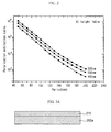
- Fig. 2 is a graph showing the relationship between the period of a wire grid an d the polarization extinction ratio in the visible light band;
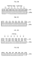
- Figs. 3A through 3E diagrammatically illustrate a process for producing a mold for manufacturing a wire grid according to the present invention;
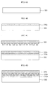
- Figs. 4A to 4H illustrate a sequence of a manufacturing process of a wire grid polarizer, according to a first embodiment of the present invention; and
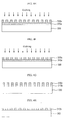
- Figs. 5A to 5G illustrate a sequence of a manufacturing process of a wire grid polarizer, according to a second embodiment of the present invention.
- The following detailed description will present a wire grid polarizer according t o a preferred embodiment of the invention in reference to the accompanying drawings.
- Fig. 2 is a graph showing the relationship between the period of a wire grid an d the polarization extinction ratio in the visible light band.
- As shown in Fig. 2, the polarization efficiency of the wire grid polarizer is in a close relationship with the period of the wire grid.
- The material of the wire grid is aluminum (Al), and the height of the wire grid i s 140nm.
- And, the line width of the wires of the grid is 60nm, the periods of the R, the G, and the B light are 450nm, 550nm, and 650nm, respectively.
- To obtain the polarization extinction ratio higher than 10,000 : 1, the grid peri od should be shorter than 120nm.
- Before manufacturing the wire grid polarizer using the embossing technique, a mold should be prepared first.
- Figs. 3A through 3E diagrammatically illustrate a process for producing a mold for manufacturing the wire grid according to the present invention.
- Preferably, the mold is made from silicon, SiO2, quartz glass, Ni, Pt, Cr, and p olymers.
- The embossing technique for use in the manufacture of the wire grid is largely divided into two types: hot embossing technique that applies heat for molding polymer; and UV embossing technique that presses the mold, and solidifies the polymer by using ultra viol et light.
- All of the above described materials can be used with the hot embossing techn ique. Particularly, quartz glass and transparent polymers which are transparent materials ca n also be used with the UV embossing technique.
- Referring to Fig. 3A, a
polymer layer 210 is sprayed or spin coated on amold s ubstrate 200, such as silicon. - Preferably, the
polymer layer 210 is made from an electron beam sensitive mat erial, PMMA (polymethylmethacrylate) for example. - Multiplexing usually occurs in the electron beam sensitive part of the polymer, and using this nature, it is possible to obtain a desired pattern through electron beam irradiati on and developing processes.
- If the polymer is a positive photosensitizer, an electron beam irradiated part m elts in the developer, while if the polymer is a negative photosensitizer, the rest of the polyme r except for the electron beam irradiated part melt in the developer.
- As shown in Fig. 3B, after the
polymer layer 210 is formed on the mold substr ate 200a, a grid pattern is formed on thepolymer layer 210 through the electron beam irradia tion. - Next, as shown in Fig. 3C, the
mold substrate 200a and thepolymer layer 210 are dipped in the developer to ensure the grid pattern is developed as it is. - As shown in Fig 3D, the grid pattern is used as an etching mask, and the mold substrate is dry etched or wet etched.
- Lastly, the polymer layer used as the etching mask is removed, and as shown in Fig. 3E, the
mold 200b with a desired pattern for manufacturing the wire grid is produced. - Here, the surface of the mold is treated with a silane-containing chemical to fa cilitate the separation of the polymer and the mold.
- Thusly prepared mold is then used for manufacturing the wire grid polarizer o perating in the visible band.
- Figs. 4A to 4H illustrate a sequence of a manufacturing process of a wire grid polarizer, according to a first embodiment of the present invention.
- As described before, the wire grid polarizer is manufactured by using the pre-made mold. To this end, a
transparent glass substrate 300 with both surfaces polished is fir st prepared (refer to Fig. 4A). - Then, as shown in Fig. 4B, a
thin metal foil 310a is deposited on the glass subs trate 300. - The
metal foil 310a can be made from Al, Ag, or Cr. - Later, the
metal foil 310a is coated with apolymer 320a, as shown in Fig. 4C. - The
polymer 320a is pressed by themold 330, and as a result, the pattern from the mold is printed onto thepolymer 320a. - Here, if the
polymer 320a is a thermosetting material, a metal mold is employe d, and if thepolymer 320a is a UV cure material, a transparent polymer mold is employed. - In the former case where the
polymer 320a is a thermosetting material, the hot embossing technique is used to pre-bake the polymer. In the later case where thepolymer 320a is a UV cure material, the UV embossing technique is used, so that the coated polymer is not cured and a transparent mold is used. - As shown in Fig. 4D, by applying heat or irradiating ultraviolet light onto the
mold 330, thepolymer 320b is cured or solidified. - Afterwards, as shown in Fig. 4E, the
mold 330 is separated from thepolymer 320b. - Then, the pattern from the
mold 330 is printed onto thepolymer 320b, that is, the polymer has an opposite pattern to the pattern from themold 330. - In case of using the hot embossing technique, the
mold 330 has to be separate d from thepolymer 320b after the temperature of the substrate is sufficiently cooled down. - In case of using the UV embossing technique, the
mold 330 is separated from thepolymer 320b after the UR curing is finished. - Next, the front surface of the
polymer 320b is dry etched to exposure the surfa ce of themetal foil 310a, as shown in Fig. 4F. - Since part of the
polymer 320c is recessed by the pattern from themold 330, a relatively thin part of thepolymer 320c is removed by the etching process, thereby exposing themetal foil 310a to the surface. - Afterwards, the exposed
metal foil 310a is dry etched or wet etched, and as a r esult, awire grid pattern 310b is formed as shown in Fig. 4G. - Finally, as shown in Fig. 4H, the
polymer 320c remaining on the wiregrid patt em 310b is removed. - In this procedure, the wire grid polarizer with a desired grin pattern on the
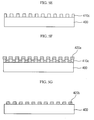
sub strate 300 is manufactured. - Figs. 5A to 5G illustrate a sequence of a manufacturing process of a wire grid polarizer, according to a second embodiment of the present invention.
- As explained before, the wire grid polarizer is manufactured by using the pre-made mold. To this end, a transparent glass substrate with both surfaces polished is first pr epared (refer to Fig. 5A).
- Later, as shown in Fig. 5B, the
glass substrate 400 is coated with apolymer 410 a, and themold 430 is prepared. - Then, the
polymer 410a is pressed by themold 430, and as a result, the pattern from themold 430 is printed onto thepolymer 410b, as shown in Fig. 5C. - The pattern printed onto the
polymer 410b is opposite to the pattern from themold 430. - As shown in Fig. 5D, by applying heat or irradiating ultraviolet light onto the
mold 430, thepolymer 410b is cured or solidified - In case of using the hot embossing technique, the
mold 430 has to be separate d from thepolymer 410b after the temperature of thesubstrate 400 is sufficiently cooled do wn. - In case of using the UV embossing technique, the
mold 430 is separated from thepolymer 410b after the UR curing is finished. - Here, if the polymer is a thermosetting material, a metal mold is employed, and if the polymer is a UV cure material, a transparent polymer mold is employed.
- In the former case where the polymer is a thermosetting material, the hot emb ossing technique is used to pre-bake the polymer. In the later case where the polymer is a UV cure material, the UV embossing technique is used, so that the coated polymer is not cur ed and a transparent mold is used.
- Afterwards, the front surface of the polymer 41cb is dry etched to exposure th e surface of the
substrate 400, as shown in Fig. 5E. - Since part of the
polymer 410c is recessed by the pattern from themold 430, a relatively thin part of thepolymer 410c is removed by the etching process, thereby exposing thesubstrate 400 to the surface. - Next, a
metal foil 420a is vacuum deposited on theglass substrate 400, as sho wn in Fig. 5F. - The
metal foil 420a can be made from Al, Ag, or Cr. - Later, the
polymer 410c with the depositedmetal foil 420a is dipped into an et chant and is removed. At the end, awire grid pattern 420b shown in Fig. 5G is obtained. - In this procedure, the wire grid polarizer with a desired grin pattern on the
sub strate 400 is manufactured. - In conclusion, the wire grid polarizer of the present invention is advantageous for reducing the manufacture cost in that it can be mass produced by using a mold over and over.
- Also, the manufacturing method of the wire grid polarizer of the present inven tion does not require additional equipment, and its process takes a short time, consequently i ncreasing yield.
- Moreover, the wire grid polarizer has the high polarization extinction ratio at v isible wavelengths, so that it can be broadly used in diverse applications such as flat displays, projection displays, optical equipment, and so on.
- While the invention has been shown and described with reference to certain pr eferred embodiments thereof, it will be understood by those skilled in the art that various cha nges in form and details may be made therein without departing from the spirit and scope of the invention as defined by the appended claims.
- The foregoing embodiments and advantages are merely exemplary and are not to be construed as limiting the present invention. The present teaching can be readily appli ed to other types of apparatuses. The description of the present invention is intended to be illustrative, and not to limit the scope of the claims. Many alternatives, modifications, and variations will be apparent to those skilled in the art. In the claims, means-plus-function claus es are intended to cover the structures described herein as performing the recited function an d not only structural equivalents but also equivalent structures.
- The claims refer to examples of preferred embodiments of the invention. How ever, the invention also refers to the use of any single feature and subcombination of features which are disclosed in the claims, the description and/or in the drawings.
Claims (19)
- A wire grid polarizer comprising:a substrate; anda wire grid pattern formed on the substrate by a mold, and having a shorter than 120n m of period for the wire grid.
- The wire grid polarizer according to claim 1, wherein a material for the mold is selecte d from a group consisting of silicon, SiO2, quartz glass, Ni, Pt, Cr, and polymers.
- The wire grid polarizer according to claim 1, wherein the wire grid pattern is printed f rom the mold by using a hot embossing or a UV embossing technique.
- A manufacturing method of a wire grid polarizer, the method comprising the steps of:preparing a mold;sequentially forming a metal foil and a polymer on a substrate;molding a polymer by using the mold;etching the metal foil by using the molded polymer, and forming a wire grid pattern; a ndremoving the polymer.
- The method according to claim 4, wherein a material for the mold is selected from a g roup consisting of silicon, SiO2, quartz glass, Ni, Pt, Cr, and polymers.
- The method according to claim 4, wherein the polymer molding step by using the mol d comprises the sub-steps of:pressing the mold to the polymer to print the pattern from the mold onto the polymer ;curing the polymer; andseparating the mold from the polymer.
- The method according to claim 4, wherein the polymer is a thermosetting material or a UV cure material.
- The method according to claim 4, wherein the step for preparing the mold comprises the sub-steps of:forming a photosensitive polymer on the mold substrate;patterning the photosensitive polymer;etching the mold substrate by using the photosensitive polymer as a mask; andremoving the photosensitive polymer.
- The method according to claim 8, wherein the photosensitive polymer is patterned by using photolithography, electron beam lithography, and semiconductor exposure processes.
- The method according to claim 4, wherein the metal foil is dry etched or wet etched.
- The method according to claim 8, wherein to remove the photosensitive polymer mor e easily, the surface of the mold is treated with a silane containing chemical.
- A manufacturing method of a wire grid polarizer, the method comprising the steps of:preparing a mold;coating a substrate with a polymer;forming a polymer pattern by using the mold;etching the polymer pattern and exposing part of the substrate;depositing a metal foil onto the polymer pattern and the exposed substrate; andremoving the polymer pattern.
- The method according to claim 12, wherein a material for the mold is selected from a group consisting of silicon, SiO2, quartz glass, Ni, Pt, Cr, and polymers.
- The method according to claim 12, wherein the step for forming the polymer pattern by using the mold comprises the sub-steps of:pressing the mold to the polymer to print the pattern from the mold onto the polymer ;curing the polymer; andseparating the mold from the polymer.
- The method according to claim 12, wherein the polymer is a thermosetting material or a UV cure material.
- The method according to claim 12, wherein the step for preparing the mold comprise s the sub-steps of:forming a photosensitive polymer on the mold substrate;patterning the photosensitive polymer;etching the mold substrate by using the photosensitive polymer as a mask; andremoving the photosensitive polymer.
- The method according to claim 16, wherein the photosensitive polymer is patterned b y using photolithography, electron beam lithography, and semiconductor exposure processes.
- The method according to claim 12, wherein the metal foil is dry etched or wet etched.
- The method according to claim 16, wherein to remove the photosensitive polymer m ore easily, the surface of the mold is treated with a silane containing chemical.
Priority Applications (1)
| Application Number | Priority Date | Filing Date | Title |
|---|---|---|---|
| EP04021773A EP1635199A1 (en) | 2004-09-14 | 2004-09-14 | Wire grid polarizer and manufacturing method thereof |
Applications Claiming Priority (1)
| Application Number | Priority Date | Filing Date | Title |
|---|---|---|---|
| EP04021773A EP1635199A1 (en) | 2004-09-14 | 2004-09-14 | Wire grid polarizer and manufacturing method thereof |
Publications (1)
| Publication Number | Publication Date |
|---|---|
| EP1635199A1 true EP1635199A1 (en) | 2006-03-15 |
Family
ID=34926524
Family Applications (1)
| Application Number | Title | Priority Date | Filing Date |
|---|---|---|---|
| EP04021773A Withdrawn EP1635199A1 (en) | 2004-09-14 | 2004-09-14 | Wire grid polarizer and manufacturing method thereof |
Country Status (1)
| Country | Link |
|---|---|
| EP (1) | EP1635199A1 (en) |
Cited By (9)
| Publication number | Priority date | Publication date | Assignee | Title |
|---|---|---|---|---|
| EP1887391A1 (en) * | 2006-08-11 | 2008-02-13 | Rohm and Haas Denmark Finance A/S | Wire grid polarizer |
| CN104460021A (en) * | 2014-12-11 | 2015-03-25 | 国家纳米科学中心 | Micro-polarizing film array and manufacturing method thereof |
| CN107450758A (en) * | 2016-05-31 | 2017-12-08 | 北京小米移动软件有限公司 | The method of pattern-making, metal shell and terminal device in metal surface |
| WO2018078174A1 (en) * | 2016-10-28 | 2018-05-03 | Valeo Comfort And Driving Assistance | Display |
| CN108062001A (en) * | 2018-01-02 | 2018-05-22 | 京东方科技集团股份有限公司 | The patterning method of film layer, wire grating polarization structure and preparation method thereof |
| US10401678B2 (en) | 2014-08-14 | 2019-09-03 | Applied Materials, Inc. | Systems, apparatus, and methods for an electromagnetic interference shielding optical polarizer |
| CN111312913A (en) * | 2020-02-20 | 2020-06-19 | 京东方科技集团股份有限公司 | Display device |
| CN111479649A (en) * | 2017-12-20 | 2020-07-31 | 索尼公司 | Laser device and laser processing method |
| CN116603700A (en) * | 2022-02-08 | 2023-08-18 | 成都拓米双都光电有限公司 | Preparation method of support grid plate |
Citations (5)
| Publication number | Priority date | Publication date | Assignee | Title |
|---|---|---|---|---|
| US5259926A (en) * | 1991-09-24 | 1993-11-09 | Hitachi, Ltd. | Method of manufacturing a thin-film pattern on a substrate |
| US5630902A (en) * | 1994-12-30 | 1997-05-20 | Honeywell Inc. | Apparatus for use in high fidelty replication of diffractive optical elements |
| US6122103A (en) * | 1999-06-22 | 2000-09-19 | Moxtech | Broadband wire grid polarizer for the visible spectrum |
| US6284072B1 (en) * | 1996-11-09 | 2001-09-04 | Epigem Limited | Multifunctional microstructures and preparation thereof |
| US20040174596A1 (en) * | 2003-03-05 | 2004-09-09 | Ricoh Optical Industries Co., Ltd. | Polarization optical device and manufacturing method therefor |
-
2004
- 2004-09-14 EP EP04021773A patent/EP1635199A1/en not_active Withdrawn
Patent Citations (5)
| Publication number | Priority date | Publication date | Assignee | Title |
|---|---|---|---|---|
| US5259926A (en) * | 1991-09-24 | 1993-11-09 | Hitachi, Ltd. | Method of manufacturing a thin-film pattern on a substrate |
| US5630902A (en) * | 1994-12-30 | 1997-05-20 | Honeywell Inc. | Apparatus for use in high fidelty replication of diffractive optical elements |
| US6284072B1 (en) * | 1996-11-09 | 2001-09-04 | Epigem Limited | Multifunctional microstructures and preparation thereof |
| US6122103A (en) * | 1999-06-22 | 2000-09-19 | Moxtech | Broadband wire grid polarizer for the visible spectrum |
| US20040174596A1 (en) * | 2003-03-05 | 2004-09-09 | Ricoh Optical Industries Co., Ltd. | Polarization optical device and manufacturing method therefor |
Cited By (12)
| Publication number | Priority date | Publication date | Assignee | Title |
|---|---|---|---|---|
| EP1887391A1 (en) * | 2006-08-11 | 2008-02-13 | Rohm and Haas Denmark Finance A/S | Wire grid polarizer |
| US10401678B2 (en) | 2014-08-14 | 2019-09-03 | Applied Materials, Inc. | Systems, apparatus, and methods for an electromagnetic interference shielding optical polarizer |
| CN104460021A (en) * | 2014-12-11 | 2015-03-25 | 国家纳米科学中心 | Micro-polarizing film array and manufacturing method thereof |
| CN107450758A (en) * | 2016-05-31 | 2017-12-08 | 北京小米移动软件有限公司 | The method of pattern-making, metal shell and terminal device in metal surface |
| WO2018078174A1 (en) * | 2016-10-28 | 2018-05-03 | Valeo Comfort And Driving Assistance | Display |
| FR3058237A1 (en) * | 2016-10-28 | 2018-05-04 | Valeo Comfort And Driving Assistance | DISPLAY |
| CN111479649A (en) * | 2017-12-20 | 2020-07-31 | 索尼公司 | Laser device and laser processing method |
| CN111479649B (en) * | 2017-12-20 | 2022-06-24 | 索尼公司 | Laser device and laser processing method |
| CN108062001A (en) * | 2018-01-02 | 2018-05-22 | 京东方科技集团股份有限公司 | The patterning method of film layer, wire grating polarization structure and preparation method thereof |
| US11009641B2 (en) | 2018-01-02 | 2021-05-18 | Boe Technology Group Co., Ltd. | Method for patterning film layer, wire grid polarizer and manufacturing method thereof |
| CN111312913A (en) * | 2020-02-20 | 2020-06-19 | 京东方科技集团股份有限公司 | Display device |
| CN116603700A (en) * | 2022-02-08 | 2023-08-18 | 成都拓米双都光电有限公司 | Preparation method of support grid plate |
Similar Documents
| Publication | Publication Date | Title |
|---|---|---|
| US20060056024A1 (en) | Wire grid polarizer and manufacturing method thereof | |
| KR100623026B1 (en) | Line lattice polarizer and its manufacturing method | |
| Priambodo et al. | Fabrication and characterization of high-quality waveguide-mode resonant optical filters | |
| KR100632510B1 (en) | Wire grid polarizer and its manufacturing method | |
| US5532089A (en) | Simplified fabrication methods for rim phase-shift masks | |
| CN111033118B (en) | Diffractive light guide plate and method of manufacturing diffractive light guide plate | |
| EP2090909B1 (en) | Wire grid polarizer and manufacturing method of the same | |
| US5245470A (en) | Polarizing exposure apparatus using a polarizer and method for fabrication of a polarizing mask by using a polarizing exposure apparatus | |
| KR100512141B1 (en) | A fabrication method of a wire grid polarizer | |
| US6569608B2 (en) | Method of manufacturing an element with multiple-level surface | |
| JP2006084776A (en) | Wire-grid polarizer and its manufacturing method | |
| EP1635199A1 (en) | Wire grid polarizer and manufacturing method thereof | |
| JP2020522021A (en) | Method of manufacturing diffraction grating | |
| JP2008074043A (en) | Mold for fine molding and its regeneration method | |
| KR100643965B1 (en) | Wire grid polarizer and its manufacturing method | |
| CN1666136A (en) | Method and apparatus for homogenous heating in an optical waveguiding structure | |
| US8092701B2 (en) | Grating, negative and replica gratings of the grating, and method of manufacturing the same | |
| JPH0799402B2 (en) | Wave plate | |
| CN1272644C (en) | Optical grating and counter grating, replica of grating and mfg. method thereof | |
| US20060257792A1 (en) | A method of structuring of a substrate | |
| CN113835214B (en) | Spectral modulation device based on spatial morphology modulation and preparation method thereof | |
| JP7671441B2 (en) | Patterned structure and method for producing same | |
| KR102861466B1 (en) | Photomask, manufacturing method of the same and manufacturing method of display device using the same | |
| CN119065212B (en) | Self-excitation photoetching method with self-alignment effect | |
| KR102261988B1 (en) | The Optical filter and The fabrication Method of The Same |
Legal Events
| Date | Code | Title | Description |
|---|---|---|---|
| PUAI | Public reference made under article 153(3) epc to a published international application that has entered the european phase |
Free format text: ORIGINAL CODE: 0009012 |
|
| 17P | Request for examination filed |
Effective date: 20040914 |
|
| AK | Designated contracting states |
Kind code of ref document: A1 Designated state(s): AT BE BG CH CY CZ DE DK EE ES FI FR GB GR HU IE IT LI LU MC NL PL PT RO SE SI SK TR |
|
| AX | Request for extension of the european patent |
Extension state: AL HR LT LV MK |
|
| 17Q | First examination report despatched |
Effective date: 20060728 |
|
| AKX | Designation fees paid |
Designated state(s): AT BE BG CH CY CZ DE DK EE ES FI FR GB GR HU IE IT LI LU MC NL PL PT RO SE SI SK TR |
|
| STAA | Information on the status of an ep patent application or granted ep patent |
Free format text: STATUS: THE APPLICATION IS DEEMED TO BE WITHDRAWN |
|
| 18D | Application deemed to be withdrawn |
Effective date: 20061208 |