EP1633015A1 - Sealing member and sealing structure of electronic circuit unit - Google Patents
Sealing member and sealing structure of electronic circuit unit Download PDFInfo
- Publication number
- EP1633015A1 EP1633015A1 EP05018907A EP05018907A EP1633015A1 EP 1633015 A1 EP1633015 A1 EP 1633015A1 EP 05018907 A EP05018907 A EP 05018907A EP 05018907 A EP05018907 A EP 05018907A EP 1633015 A1 EP1633015 A1 EP 1633015A1
- Authority
- EP
- European Patent Office
- Prior art keywords
- cable
- mounting portion
- sealing member
- circumferential mounting
- insertion hole
- Prior art date
- Legal status (The legal status is an assumption and is not a legal conclusion. Google has not performed a legal analysis and makes no representation as to the accuracy of the status listed.)
- Granted
Links
Images


Classifications
-
- H—ELECTRICITY
- H01—ELECTRIC ELEMENTS
- H01Q—ANTENNAS, i.e. RADIO AERIALS
- H01Q1/00—Details of, or arrangements associated with, antennas
- H01Q1/42—Housings not intimately mechanically associated with radiating elements, e.g. radome
-
- H—ELECTRICITY
- H05—ELECTRIC TECHNIQUES NOT OTHERWISE PROVIDED FOR
- H05K—PRINTED CIRCUITS; CASINGS OR CONSTRUCTIONAL DETAILS OF ELECTRIC APPARATUS; MANUFACTURE OF ASSEMBLAGES OF ELECTRICAL COMPONENTS
- H05K5/00—Casings, cabinets or drawers for electric apparatus
- H05K5/06—Hermetically-sealed casings
- H05K5/061—Hermetically-sealed casings sealed by a gasket held between a removable cover and a body, e.g. O-ring, packing
-
- H—ELECTRICITY
- H05—ELECTRIC TECHNIQUES NOT OTHERWISE PROVIDED FOR
- H05K—PRINTED CIRCUITS; CASINGS OR CONSTRUCTIONAL DETAILS OF ELECTRIC APPARATUS; MANUFACTURE OF ASSEMBLAGES OF ELECTRICAL COMPONENTS
- H05K5/00—Casings, cabinets or drawers for electric apparatus
- H05K5/06—Hermetically-sealed casings
- H05K5/069—Other details of the casing, e.g. wall structure, passage for a connector, a cable, a shaft
Landscapes
- Engineering & Computer Science (AREA)
- Microelectronics & Electronic Packaging (AREA)
- Details Of Aerials (AREA)
Abstract

Description
- The present invention relates to a sealing member to be mounted to a fitting portion between a pair of cases and a cable socket, and relates to a sealing structure of an electronic circuit unit, in which gaps are sealed with the sealing member.
- In electronic circuit units, such as an antenna device having a low-noise amplifier circuit and an antenna element which are unitized with the antenna device, within a casing formed by fitting a pair of cases to each other, an electronic circuit, such as a circuit board, is accommodated, and a signal cable connected to the electronic circuit may be drawn out therefrom via a cable socket arranged adjacent to the fitting portion between the pair of cases. Thus, in order to secure dust-proof and water-proof of such an electronic circuit unit, a sealing member is required for sealing gaps generated in a fitting portion between a pair of cases and the cable socket.
- As a sealing structure of such an electronic circuit unit, a technique has been generally adopted to use a first sealing member, such as an O-ring, mounted on the fitting portion all round and a second sealing member armored at a predetermined position of a signal cable so as to be mounted in the cable socket in combination (see Japanese Unexamined Patent Application Publication No. 10-276020 (
p 2, Fig. 13)). - However, in an assemble process of the electronic circuit unit adopting the sealing structure using the first sealing member with the second sealing member described above, before fitting the pair of cases to each other, it is necessary to arrange the first sealing member in the fitting portion and to armor the second sealing member at a predetermined position of the signal cable so as to be arranged in the cable socket. These two sealing members must be separately handled, so that assembling the sealing members has been complicated. Also, in the conventional sealing structure, there has been a problem that a reliable sealing structure is difficult to be achieved because a gap may be produced between the first and second sealing members.
- The present invention has been made in view of such situations of conventional techniques, and it is a first object thereof to provide a sealing member that is easily assembled and has a high sealing effect in a cable socket. Also it is a second object of the present invention to provide a sealing structure of an electronic circuit unit with a high sealing effect in the cable socket and having a sealing member that is easily assembled.
- In order to achieve the first object mentioned above, a sealing member made of an elastic molding according to the present invention includes an annular circumferential mounting portion to be mounted in a fitting portion between a pair of cases constituting a casing; and a cable insertion portion to be mounted in a cable socket of the casing adjacent to the fitting portion, in which the cable insertion portion is provided with an insertion hole for inserting a signal cable, and the cable insertion portion is rotatable on a plane substantially perpendicular to an extending direction of the part of the circumferential mounting portion adjacent to the cable insertion portion, and in which in a no-load state, the axial direction of the insertion hole corresponds to that of the circumferential mounting portion.
- Because the annular circumferential mounting portion to be mounted in the fitting portion between the pair of cases is formed integrally with the cable insertion portion to be mounted to the cable socket, the sealing member constructed as described above can be easily assembled in comparison with a case where different two sealing members are separately assembled. Since no gap is produced between the circumferential mounting portion and the cable insertion portion, the sealing in the cable socket is also effective. Moreover, in a no-load state of the sealing member, the axial direction of the insertion hole substantially corresponds to that of the circumferential mounting portion, so that a slide core can be eliminated and the sealing member is manufactured at low cost with a simple metallic mold.
- During assembling the sealing member constructed as described above in sealing portions, it is preferable that the cable insertion portion in a state elastically rotated by about 90° on the plane be mounted into the cable socket, so that the axial direction of the insertion hole be established to be substantially perpendicular to that of the circumferential mounting portion. Thereby, the extending direction of the signal cable in the cable socket can be established to be substantially perpendicular to the height direction of the casing, so that the coaxial cable is easily routed.
- In order to achieve the second object mentioned above, a sealing structure of an electronic circuit unit according to the present invention includes a casing formed by fitting a pair of cases to each other and having a cable socket arranged adjacent to a fitting portion between the pair of cases; an electronic circuit accommodated within an interior space of the casing; a signal cable connected to the electronic circuit and being outside taken through the cable socket; and a sealing member made of an elastic molding, in which the sealing member includes an annular circumferential mounting portion mounted in the fitting portion and a cable insertion portion mounted in the cable socket and having an insertion hole for inserting the signal cable, and the axial direction of the insertion hole is established to be substantially perpendicular to that of the circumferential mounting portion.
- Using the sealing member having the circumferential mounting portion molded integrally with the cable insertion portion in such a manner enables clearances generated in the fitting portion between the pair of cases and generated in the cable socket to be sealed together, so that the sealing member can be easily assembled, improving assembling efficiency of the electronic circuit unit. Since no gap is produced between the circumferential mounting portion and the cable insertion portion, the sealing in the cable socket is effective, achieving a reliable sealing structure. Moreover, since the axial direction of the insertion hole of the sealing member is established to be substantially perpendicular to that of the circumferential mounting portion, the extending direction of the signal cable in the cable socket can be established to be substantially perpendicular to the height direction of the casing, so that the coaxial cable is easily routed.
- In such a sealing structure of an electronic circuit unit, in the sealing member before being mounted in the fitting portion and the cable socket, the cable insertion portion is rotatable on a plane substantially perpendicular to an extending direction of the part of the circumferential mounting portion adjacent to the cable insertion portion while the axial direction of the insertion hole substantially corresponds to that of the circumferential mounting portion, and it is preferable that the cable insertion portion in a state elastically rotated by about 90° on the plane be mounted into the cable socket, so that the axial direction of the insertion hole be established to be substantially perpendicular to that of the circumferential mounting portion. Thereby, a slide core can be eliminated, so that the sealing member is manufactured at low cost with a simple metallic mold.
-
- Fig. 1 is a sectional view showing the entire structure of an antenna device according to an embodiment of the present invention;
- Fig. 2 is a perspective view of the antenna device viewed from the bottom surface;
- Fig. 3 is a perspective view of the antenna device showing a state of Fig. 2 from which a reflection plate is removed;
- Fig. 4 is a perspective view of a sealing member to be assembled in the antenna device;
- Fig. 5 is a perspective view of the body of the antenna device;
- Fig. 6 is an exploded perspective view of the body;
- Fig. 7 is a sectional view of the body at the line A-A of Fig. 5; and
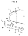
- Fig. 8 is an enlarged view of B region of Fig. 5.
- Embodiments of the present invention will be described with reference to the drawings. Fig. 1 is a sectional view of the entire structure of an antenna device (antenna unit) according to an embodiment of the present invention; Fig. 2 is a perspective view of the antenna device viewed from the bottom side; Fig. 3 is a perspective view of a state in that a reflection plate is removed from Fig. 2; Fig. 4 is perspective view of a sealing member to be assembled to the antenna device; Fig. 5 is a perspective view showing a body of the antenna device; Fig. 6 is an exploded and perspective of the body; Fig. 7 is a sectional view of the body at the line A-A of Fig. 5; and Fig. 8 is an enlarged view of region B of Fig. 5.
- The antenna device shown in these figures mainly includes a
casing 1 formed by fitting aradome 2 which is an upper case to areflection plate 3 which is a lower case, a sealing member 4 mounted in a fitting portion between theradome 2 and thereflection plate 3, a magnet 5 attached on the bottom surface of thereflection plate 3, abody 6 accommodated within an interior space of thecasing 1, and acoaxial cable 7 for electrically connecting thebody 6 to an external circuit (a receiving circuit) (not shown). Thebody 6 includes acircuit board 8 having an electronic circuit such as a low-noise amplifier circuit, anantenna element 9 that is a sheet plate patch antenna, and a metallic plate shielding case 10 (see Fig. 6). Aground pattern 11 arranged on the substantially entire surface of thecircuit board 8 opposes aconductor plate 12 of theantenna element 9 with a predetermined space therebetween. On the bottom surface of thecircuit board 8, a wiring pattern (not shown) is arranged while variouselectronic components 13 connected to the wiring pattern are mounted, so that theelectronic components 13 and the wiring pattern constitute the electronic circuit. - The
radome 2 is a synthetic resin molding and has a lower opening so as to cover thebody 6. Thereflection plate 3 is formed by pressing a metallic plate and covers the lower opening of theradome 2. Thereflection plate 3 is provided with arecess 3a formed at the center of the bottom surface, and within therecess 3a, the magnet 5 is fixed (however, the magnet 5 is omitted in Fig. 2). In addition, thereflection plate 3 is established in size to be slightly larger than theconductor plate 12 of theantenna element 9. Thecasing 1 is assembled by fitting theradome 2 to thereflection plate 3, and between theradome 2 and thereflection plate 3, a substantiallyrectangular fitting portion 1a and acable socket 1b adjacent to thefitting portion 1a are formed. As shown in Fig. 3, an annularcircumferential mounting portion 4a of the sealing member 4 is mounted on thefitting portion 1a, and acable insertion portion 4b of the sealing member 4 is mounted on acable socket 1b, so that gaps existing in thefitting portion 1a and thecable socket 1b are sealed. - The sealing member 4 is a molding made of an elastic material, such as an elastomer, and in a state of a single article before being assembled with the casing 1 (a no-load state), it has a shape shown in Fig. 4, which is molded of the annular
circumferential mounting portion 4a integrally with thecable insertion portion 4b. That is, the annularcircumferential mounting portion 4a is substantially rectangular frame-shaped similarly to thefitting portion 1a in shape. Thecable insertion portion 4b is a convex object with an external shape fitting thecable socket 1b and having aninsertion hole 4c formed therein. The axial direction of theinsertion hole 4c corresponds to the axial direction of the annularcircumferential mounting portion 4a. Since the annularcircumferential mounting portion 4a is continuously connected to corners of thecable insertion portion 4b, thecable insertion portion 4b, as shown in arrow C of Fig. 4, is rotatable on a plane substantially perpendicular to the extending direction of the part adjacent to thecable insertion portion 4b of the annularcircumferential mounting portion 4a. Theinsertion hole 4c of thecable insertion portion 4b is for inserting thecoaxial cable 7 therethrough. When the sealing member 4 is assembled in thecasing 1, after thecoaxial cable 7 is inserted into theinsertion hole 4c and thecable insertion portion 4b is mounted into thecable socket 1b in a state of thecable insertion portion 4b elastically rotated by about 90° in arrow C direction, the annularcircumferential mounting portion 4a is mounted in thefitting portion 1a. Thereby, as shown in Fig. 3, the axial direction of theinsertion hole 4c can be established to be substantially perpendicular to the axial direction of the annularcircumferential mounting portion 4a (the height direction of the casing 1), so that thecoaxial cable 7 is easily routed. - The
body 6 of the antenna device will be described. The wiring pattern formed on the bottom surface of thecircuit board 8 is provided with acentral conductor 7a of thecoaxial cable 7 soldered thereon, and on the bottom surface of thecircuit board 8, four solder lands 14 (see Fig. 7) are provided electrically independently from the wiring pattern. Furthermore, as shown in Fig. 6, thecircuit board 8 is provided with a plurality of throughholes 8a formed at positions including those corresponding to thesolder lands 14 as well as a plurality ofconcave notches 8b formed in the periphery. - The
antenna element 9 includes theradiation conductor plate 12 opposing theground pattern 11 with an air layer therebetween, fourmounting legs 15 formed by cutting up theradiation conductor plate 12 except its center toward thecircuit board 8, and two power-feeding pieces 16 formed by cutting up theradiation conductor plate 12 adjacent to its center toward thecircuit board 8. The fourmounting legs 15 and the two power-feeding pieces 16 are inserted into the corresponding through-holes 8a and soldered on the bottom surface of thecircuit board 8. Themounting legs 15 are connected to thesolder lands 14 while the power-feeding pieces 16 are connected to the wiring pattern. As shown in Fig. 7, at the end of themounting leg 15, anelastic hook 15a is formed, and by pressing theelastic hook 15a, themounting leg 15 is retained to thecircuit board 8. Hence, by pressing themounting legs 15 into the corresponding through-holes 8a, theantenna element 9 can be temporarily fixed to thecircuit board 8 simply and precisely. Theantenna element 9 is finally fixed to thecircuit board 8 by soldering the thus self-sustainedantenna device 9 in a reflow furnace. - The shielding
case 10 covers theelectronic components 13 of the low-noise amplifier circuit, so that antenna characteristic deterioration by undesired electric waves radiated from the low-noise amplifier circuit is reduced as well as possibilities of bad influence on the low-noise amplifier circuit from external interfering waves are reduced to a large extent, securing high reliability. The shieldingcase 10 is provided with a plurality of get-awayholes 10a formed at positions opposing soldering portions on the bottom surface of thecircuit board 8. In the periphery of the shieldingcase 10, a plurality ofelastic retainers 10b are upward protruded, which are soldered to theground pattern 11 on the top surface of thecircuit board 8 after being snap-fitted into the correspondingnotches 8b of thecircuit board 8. In this case, also by snap-fitting theelastic retainers 10b into the correspondingnotches 8b, the shieldingcase 10 can be temporarily fixed to thecircuit board 8 simply and precisely, so as to be finally fixed to thecircuit board 8 by soldering the thus self-sustainedshielding case 10 in a reflow furnace. At a predetermined position of the periphery of the shieldingcase 10, a substantially U-shapedcable holding portion 10c is formed by cutting down therefrom so as to position the end portion of the coaxial cable 7 (see Fig. 3). - The antenna device constructed as described above can be operated as a circular polarized antenna by two-point feeding power to the
radiation conductor plate 12 via the two power-feedingpieces 16 connected to the wiring pattern of thecircuit board 8. That is, when a predetermined highfrequency signal is fed to theradiation conductor plate 12 via the low-noise amplifier circuit, circular polarized radio waves are radiated from theradiation conductor plate 12, and when the signal radio waves are received by theradiation conductor plate 12, the electric signal is outputted to external receiver circuits via the low-noise amplifier circuit and thecoaxial cable 7. - In the antenna device according to the embodiment, the
body 6 including thecircuit board 8 and theradiation conductor plate 12 is accommodated within thecasing 1 as well as the sealing member 4 is mounted in thefitting portion 1a and thecable socket 1b of thecasing 1, enabling dust proof and water proof to be secured. Moreover, the sealing member 4 can be easily assembled in comparison with a case where different two sealing members are separately assembled, because the annularcircumferential mounting portion 4a of the sealing member 4 to be mounted in thefitting portion 1a is formed integrally with thecable insertion portion 4b to be mounted to thecable socket 1b. Furthermore, since no gap is produced between the annularcircumferential mounting portion 4a and thecable insertion portion 4b, the sealing in thecable socket 1b is also effective. Therefore, by adopting such a sealing structure, reduction in assembling cost and improvement in dust/water proof may be promised. Also, because in the sealing member 4 in a no-load state, the axial direction of theinsertion hole 4c corresponds to the axial direction of the annularcircumferential mounting portion 4a, a slide core can be eliminated by directing the die opening in this axial direction, so that the sealing member 4 is manufactured at low cost with a simple metallic mold. Moreover, during assembling the sealing member 4 in thecasing 1, by mounting thecable insertion portion 4b into thecable socket 1b in an elastically rotated state, the axial direction of theinsertion hole 4c can be established to be substantially perpendicular to the axial direction (the height direction of the casing 1) of the annularcircumferential mounting portion 4a, so that thecoaxial cable 7 can be easily routed. - In the antenna device according to the embodiment, since the
solder land 14, on which the mountingleg 15 of theradiation conductor plate 12 is soldered, opposes theground pattern 11 with thecircuit board 8 therebetween, an additional capacitance is generated between thesolder land 14 and theground pattern 11, so that the resonance frequency is reduced, enabling theantenna element 9 to be miniaturized. Because the resonance frequency is varied in accordance with sizes and the arrangement of a plurality of solder lands 14, the resonance frequency can be comparatively easily micro-adjusted and broadened. Furthermore, the antenna device uses themetallic reflection plate 3 as the lower case, so that by reflecting radio waves with thereflection plate 3, the radiations in undesired directions are suppressed, increasing gain. Moreover, since the magnet 5 is fixed within therecess 3a on the bottom surface of thereflection plate 3, the antenna device can be easily attached to arbitrary positions in both the outside and inside vehicle cabin where a metal is embedded or exposed. - In the antenna device according to the embodiment, the
antenna element 9 before the soldering process can be self-sustained on thecircuit board 8 by pressing theelastic hook 15a of the mountingleg 15 into the through-hole 8a while the shieldingcase 10 before the soldering process can be self-sustained on thecircuit board 8 by snap-fitting theelastic retainers 10b into thenotches 8b, so that theantenna element 9 and the shieldingcase 10 can be reflow-soldered together. That is, in the assemble process of the antenna device, after cream solder is applied to predetermined positions of thecircuit board 8, at which the mountinglegs 15 and the power-feedingpieces 16 are soldered, theantenna element 9 and the shieldingcase 10 are attached on thecircuit board 8; at this time, since theantenna element 9 is temporarily fixed by the retaining of theelastic hook 15a, theantenna element 9 and the shieldingcase 10 can be reflow-soldered together in a self-sustained state on thecircuit board 8. Doing so enables the number of processes to be reduced in comparison with a case where theantenna element 9 and the shieldingcase 10 are separately reflow-soldered, reducing assembling cost to a large extent. Also, in the antenna device, because theantenna element 9 is a sheet-metal patch antenna, the component cost can be obviously reduced less than that of a dielectric antenna. - In addition, according to the embodiment, the sealing structure of the antenna device (antenna unit) has been described; alternatively, other electronic circuit units having signal cables, such as a lead-out coaxial cable, may also have the same advantages as those of the embodiment by using a sealing member made by integrally molding an annular circumferential mounting portion of the sealing member to be mounted in a fitting portion with a cable insertion portion thereof to be mounted to a cable socket.
Claims (4)
- A sealing member made of an elastic molding comprising:an annular circumferential mounting portion to be mounted in a fitting portion between a pair of cases constituting a casing; anda cable insertion portion to be mounted in a cable socket of the casing adjacent to the fitting portion,and the cable insertion portion is rotatable on a plane substantially perpendicular to an extending direction of the part of the circumferential mounting portion adjacent to the cable insertion portion, andwherein in a no-load state, the axial direction of the insertion hole substantially corresponds to that of the circumferential mounting portion.
- The member according to Claim 1, wherein the cable insertion portion in an elastically rotated state by about 90° on the plane is mounted into the cable socket, so that the axial direction of the insertion hole is established to be substantially perpendicular to that of the circumferential mounting portion.
- A sealing structure of an electronic circuit unit comprising:a casing formed by fitting a pair of cases to each other and having a cable socket arranged adjacent to a fitting portion between the pair of cases;an electronic circuit accommodated within an interior space of the casing;a signal cable connected to the electronic circuit and being outside taken through the cable socket; anda sealing member made of an elastic molding,wherein the sealing member includes an annular circumferential mounting portion mounted in the fitting portion and a cable insertion portion mounted in the cable socket and having an insertion hole for inserting the signal cable, andwherein the axial direction of the insertion hole is established to be substantially perpendicular to that of the circumferential mounting portion.
- The structure according to Claim 3, wherein in the sealing member before being mounted in the fitting portion and the cable socket, the cable insertion portion is rotatable on a plane substantially perpendicular to an extending direction of the part of the circumferential mounting portion adjacent to the cable insertion portion while the axial direction of the insertion hole substantially corresponds to that of the circumferential mounting portion, and
wherein the cable insertion portion in a state elastically rotated by about 90° on the plane is mounted into the cable socket, so that the axial direction of the insertion hole is established to be substantially perpendicular to that of the circumferential mounting portion.
Applications Claiming Priority (1)
| Application Number | Priority Date | Filing Date | Title |
|---|---|---|---|
| JP2004254246A JP4148934B2 (en) | 2004-09-01 | 2004-09-01 | Seal member and seal structure of electronic circuit unit |
Publications (2)
| Publication Number | Publication Date |
|---|---|
| EP1633015A1 true EP1633015A1 (en) | 2006-03-08 |
| EP1633015B1 EP1633015B1 (en) | 2008-05-14 |
Family
ID=34979364
Family Applications (1)
| Application Number | Title | Priority Date | Filing Date |
|---|---|---|---|
| EP20050018907 Expired - Fee Related EP1633015B1 (en) | 2004-09-01 | 2005-08-31 | Sealing member and sealing structure of electronic circuit unit |
Country Status (3)
| Country | Link |
|---|---|
| EP (1) | EP1633015B1 (en) |
| JP (1) | JP4148934B2 (en) |
| DE (1) | DE602005006683D1 (en) |
Cited By (10)
| Publication number | Priority date | Publication date | Assignee | Title |
|---|---|---|---|---|
| EP1863124A1 (en) * | 2006-05-30 | 2007-12-05 | Nippon Sheet Glass Company, Limited | On-board antenna device |
| EP1930979A1 (en) * | 2006-12-05 | 2008-06-11 | Delphi Technologies, Inc. | High frequency capacitive coupling antenna for vehicles |
| EP2654271A1 (en) * | 2012-04-16 | 2013-10-23 | Sony Mobile Communications Japan, Inc. | Gasket Structure and Terminal Device |
| US20130286597A1 (en) * | 2012-04-27 | 2013-10-31 | Delta Electronics, Inc. | Waterproof controller used for electric power steering |
| EP2882055A1 (en) * | 2013-12-04 | 2015-06-10 | LSIS Co., Ltd. | Electric vehicle charger |
| WO2016000519A1 (en) * | 2014-06-30 | 2016-01-07 | 华为技术有限公司 | Radio-frequency module waterproof structure and radio-frequency module having same |
| DE102008042811B4 (en) * | 2008-10-14 | 2018-02-22 | Blaupunkt Antenna Systems Gmbh & Co. Kg | Roof antenna for a vehicle and method for producing such a roof antenna |
| CN108232402A (en) * | 2017-01-12 | 2018-06-29 | 原田工业株式会社 | Antenna assembly |
| US10303078B2 (en) | 2017-09-27 | 2019-05-28 | Fuji Xerox Co., Ltd. | Image forming apparatus having two transfer units |
| US10359730B2 (en) | 2017-09-27 | 2019-07-23 | Fuji Xerox Co., Ltd. | Image forming apparatus having developer with carrier |
Families Citing this family (3)
| Publication number | Priority date | Publication date | Assignee | Title |
|---|---|---|---|---|
| JP4892304B2 (en) * | 2006-09-01 | 2012-03-07 | 古野電気株式会社 | Observation device and land displacement monitoring system |
| JP2016223948A (en) * | 2015-06-01 | 2016-12-28 | サカエ理研工業株式会社 | Vehicle radome and vehicle radar device |
| CN106332483A (en) * | 2015-06-19 | 2017-01-11 | 梁北洪 | Electric cabinet apparatus used for numerical control equipment |
Citations (5)
| Publication number | Priority date | Publication date | Assignee | Title |
|---|---|---|---|---|
| US5625365A (en) * | 1995-03-10 | 1997-04-29 | Trimble Navigation Limited | Dual-frequency microwave radio antenna system |
| US5670745A (en) * | 1993-12-27 | 1997-09-23 | Mitsumi Electric Co., Ltd. | Hermetically sealed case sealed by packing |
| JPH10276020A (en) | 1997-03-31 | 1998-10-13 | Mitsumi Electric Co Ltd | Plane antenna |
| EP1033779A2 (en) * | 1999-03-04 | 2000-09-06 | Alps Electric Co., Ltd. | Converter provided with built-in patch antennas for receiving direct broadcasting by satellite |
| EP1253665A2 (en) * | 2001-04-25 | 2002-10-30 | Alps Electric Co., Ltd. | Waterproof structure of antenna |
Family Cites Families (3)
| Publication number | Priority date | Publication date | Assignee | Title |
|---|---|---|---|---|
| JPH0638308U (en) * | 1992-10-15 | 1994-05-20 | 松下電工株式会社 | Antenna unit |
| JP3508352B2 (en) * | 1995-12-15 | 2004-03-22 | 松下電工株式会社 | Antenna device |
| JP2002319772A (en) * | 2001-04-23 | 2002-10-31 | Aisin Seiki Co Ltd | Closed unit |
-
2004
- 2004-09-01 JP JP2004254246A patent/JP4148934B2/en not_active Expired - Fee Related
-
2005
- 2005-08-31 EP EP20050018907 patent/EP1633015B1/en not_active Expired - Fee Related
- 2005-08-31 DE DE200560006683 patent/DE602005006683D1/en active Active
Patent Citations (5)
| Publication number | Priority date | Publication date | Assignee | Title |
|---|---|---|---|---|
| US5670745A (en) * | 1993-12-27 | 1997-09-23 | Mitsumi Electric Co., Ltd. | Hermetically sealed case sealed by packing |
| US5625365A (en) * | 1995-03-10 | 1997-04-29 | Trimble Navigation Limited | Dual-frequency microwave radio antenna system |
| JPH10276020A (en) | 1997-03-31 | 1998-10-13 | Mitsumi Electric Co Ltd | Plane antenna |
| EP1033779A2 (en) * | 1999-03-04 | 2000-09-06 | Alps Electric Co., Ltd. | Converter provided with built-in patch antennas for receiving direct broadcasting by satellite |
| EP1253665A2 (en) * | 2001-04-25 | 2002-10-30 | Alps Electric Co., Ltd. | Waterproof structure of antenna |
Non-Patent Citations (1)
| Title |
|---|
| PATENT ABSTRACTS OF JAPAN vol. 1999, no. 01 29 January 1999 (1999-01-29) * |
Cited By (16)
| Publication number | Priority date | Publication date | Assignee | Title |
|---|---|---|---|---|
| EP1863124A1 (en) * | 2006-05-30 | 2007-12-05 | Nippon Sheet Glass Company, Limited | On-board antenna device |
| US7576700B2 (en) | 2006-05-30 | 2009-08-18 | Nippon Sheet Glass Company Limited | On-board antenna device |
| EP1930979A1 (en) * | 2006-12-05 | 2008-06-11 | Delphi Technologies, Inc. | High frequency capacitive coupling antenna for vehicles |
| US7592960B2 (en) | 2006-12-05 | 2009-09-22 | Delphi Technologies, Inc. | High frequency capacitive coupling antenna for vehicles |
| DE102008042811B4 (en) * | 2008-10-14 | 2018-02-22 | Blaupunkt Antenna Systems Gmbh & Co. Kg | Roof antenna for a vehicle and method for producing such a roof antenna |
| US9185193B2 (en) | 2012-04-16 | 2015-11-10 | Sony Corporation | Gasket structure for a terminal apparatus |
| EP2654271A1 (en) * | 2012-04-16 | 2013-10-23 | Sony Mobile Communications Japan, Inc. | Gasket Structure and Terminal Device |
| US9042102B2 (en) * | 2012-04-27 | 2015-05-26 | Delta Electronics, Inc. | Waterproof controller used for electric power steering |
| US20130286597A1 (en) * | 2012-04-27 | 2013-10-31 | Delta Electronics, Inc. | Waterproof controller used for electric power steering |
| EP2882055A1 (en) * | 2013-12-04 | 2015-06-10 | LSIS Co., Ltd. | Electric vehicle charger |
| US9764651B2 (en) | 2013-12-04 | 2017-09-19 | Lsis Co., Ltd. | Electric vehicle charger |
| WO2016000519A1 (en) * | 2014-06-30 | 2016-01-07 | 华为技术有限公司 | Radio-frequency module waterproof structure and radio-frequency module having same |
| CN108232402A (en) * | 2017-01-12 | 2018-06-29 | 原田工业株式会社 | Antenna assembly |
| US10658742B2 (en) | 2017-01-12 | 2020-05-19 | Harada Industry Co., Ltd. | Antenna device |
| US10303078B2 (en) | 2017-09-27 | 2019-05-28 | Fuji Xerox Co., Ltd. | Image forming apparatus having two transfer units |
| US10359730B2 (en) | 2017-09-27 | 2019-07-23 | Fuji Xerox Co., Ltd. | Image forming apparatus having developer with carrier |
Also Published As
| Publication number | Publication date |
|---|---|
| JP2006074349A (en) | 2006-03-16 |
| EP1633015B1 (en) | 2008-05-14 |
| JP4148934B2 (en) | 2008-09-10 |
| DE602005006683D1 (en) | 2008-06-26 |
Similar Documents
| Publication | Publication Date | Title |
|---|---|---|
| EP1633015B1 (en) | Sealing member and sealing structure of electronic circuit unit | |
| EP1641074B1 (en) | Antenna device | |
| JP4323440B2 (en) | Antenna device | |
| EP1102347B1 (en) | Integrated antenna ground plate and EMC shield structure | |
| US6181573B1 (en) | Two-part electromagnetic radiation shielding device for mounting on a printed circuit board | |
| EP1501202B1 (en) | Internal antenna and mobile terminal having the internal antenna | |
| EP3261173B1 (en) | Communication device and antenna assembly thereof | |
| US8213660B2 (en) | Shielded microphone for mobile communications device | |
| US20080166921A1 (en) | Shielded connector | |
| US7442082B2 (en) | Shielded connector with folding arrangement ensuring perpendicularity between sidewall and bottom wall of the metal housing | |
| US20100033940A1 (en) | Inter-board coupling connector and circuit board device using inter-board coupling connector | |
| US20030119347A1 (en) | Shielded connector assembly and shielded connector | |
| US7559799B2 (en) | Electrical connector | |
| CN109075435B (en) | Two-part antenna element | |
| US7825341B2 (en) | Antenna device and shield cover thereof | |
| US7247053B2 (en) | High-frequency apparatus having high performance and capable of preventing entry of interfering wave into terminal | |
| US7151503B2 (en) | Antenna unit | |
| EP1843625B1 (en) | Shielded Microphone for Mobile Communications Device | |
| JPH07142906A (en) | Cover body fitting structure for dielectric filter | |
| JP3429597B2 (en) | Small radio | |
| JP3873684B2 (en) | Wireless communication equipment | |
| JP2020145562A (en) | Vehicle communication device | |
| JP2005268899A (en) | Antenna mounting structure of mobile communication apparatus | |
| KR20180118433A (en) | Receptacle connector | |
| JP2002118382A (en) | High-frequency unit |
Legal Events
| Date | Code | Title | Description |
|---|---|---|---|
| PUAI | Public reference made under article 153(3) epc to a published international application that has entered the european phase |
Free format text: ORIGINAL CODE: 0009012 |
|
| AK | Designated contracting states |
Kind code of ref document: A1 Designated state(s): AT BE BG CH CY CZ DE DK EE ES FI FR GB GR HU IE IS IT LI LT LU LV MC NL PL PT RO SE SI SK TR |
|
| AX | Request for extension of the european patent |
Extension state: AL BA HR MK YU |
|
| 17P | Request for examination filed |
Effective date: 20060206 |
|
| AKX | Designation fees paid |
Designated state(s): DE FR GB |
|
| GRAP | Despatch of communication of intention to grant a patent |
Free format text: ORIGINAL CODE: EPIDOSNIGR1 |
|
| GRAS | Grant fee paid |
Free format text: ORIGINAL CODE: EPIDOSNIGR3 |
|
| GRAA | (expected) grant |
Free format text: ORIGINAL CODE: 0009210 |
|
| AK | Designated contracting states |
Kind code of ref document: B1 Designated state(s): DE FR GB |
|
| REG | Reference to a national code |
Ref country code: GB Ref legal event code: FG4D |
|
| REF | Corresponds to: |
Ref document number: 602005006683 Country of ref document: DE Date of ref document: 20080626 Kind code of ref document: P |
|
| PLBE | No opposition filed within time limit |
Free format text: ORIGINAL CODE: 0009261 |
|
| STAA | Information on the status of an ep patent application or granted ep patent |
Free format text: STATUS: NO OPPOSITION FILED WITHIN TIME LIMIT |
|
| 26N | No opposition filed |
Effective date: 20090217 |
|
| PGFP | Annual fee paid to national office [announced via postgrant information from national office to epo] |
Ref country code: DE Payment date: 20110831 Year of fee payment: 7 Ref country code: GB Payment date: 20110722 Year of fee payment: 7 Ref country code: FR Payment date: 20110811 Year of fee payment: 7 |
|
| GBPC | Gb: european patent ceased through non-payment of renewal fee |
Effective date: 20120831 |
|
| REG | Reference to a national code |
Ref country code: FR Ref legal event code: ST Effective date: 20130430 |
|
| PG25 | Lapsed in a contracting state [announced via postgrant information from national office to epo] |
Ref country code: DE Free format text: LAPSE BECAUSE OF NON-PAYMENT OF DUE FEES Effective date: 20130301 Ref country code: GB Free format text: LAPSE BECAUSE OF NON-PAYMENT OF DUE FEES Effective date: 20120831 |
|
| PG25 | Lapsed in a contracting state [announced via postgrant information from national office to epo] |
Ref country code: FR Free format text: LAPSE BECAUSE OF NON-PAYMENT OF DUE FEES Effective date: 20120831 |
|
| REG | Reference to a national code |
Ref country code: DE Ref legal event code: R119 Ref document number: 602005006683 Country of ref document: DE Effective date: 20130301 |