EP1631903B1 - Generation de decalage d'adresse dans un systeme de traitement de donnees - Google Patents
Generation de decalage d'adresse dans un systeme de traitement de donnees Download PDFInfo
- Publication number
- EP1631903B1 EP1631903B1 EP03782716A EP03782716A EP1631903B1 EP 1631903 B1 EP1631903 B1 EP 1631903B1 EP 03782716 A EP03782716 A EP 03782716A EP 03782716 A EP03782716 A EP 03782716A EP 1631903 B1 EP1631903 B1 EP 1631903B1
- Authority
- EP
- European Patent Office
- Prior art keywords
- bit
- values
- address offset
- offset
- value
- Prior art date
- Legal status (The legal status is an assumption and is not a legal conclusion. Google has not performed a legal analysis and makes no representation as to the accuracy of the status listed.)
- Expired - Lifetime
Links
Images

Classifications
-
- G—PHYSICS
- G06—COMPUTING OR CALCULATING; COUNTING
- G06F—ELECTRIC DIGITAL DATA PROCESSING
- G06F9/00—Arrangements for program control, e.g. control units
- G06F9/06—Arrangements for program control, e.g. control units using stored programs, i.e. using an internal store of processing equipment to receive or retain programs
- G06F9/30—Arrangements for executing machine instructions, e.g. instruction decode
- G06F9/34—Addressing or accessing the instruction operand or the result ; Formation of operand address; Addressing modes
- G06F9/342—Extension of operand address space
-
- G—PHYSICS
- G06—COMPUTING OR CALCULATING; COUNTING
- G06F—ELECTRIC DIGITAL DATA PROCESSING
- G06F9/00—Arrangements for program control, e.g. control units
- G06F9/06—Arrangements for program control, e.g. control units using stored programs, i.e. using an internal store of processing equipment to receive or retain programs
- G06F9/30—Arrangements for executing machine instructions, e.g. instruction decode
- G06F9/30145—Instruction analysis, e.g. decoding, instruction word fields
- G06F9/30149—Instruction analysis, e.g. decoding, instruction word fields of variable length instructions
-
- G—PHYSICS
- G06—COMPUTING OR CALCULATING; COUNTING
- G06F—ELECTRIC DIGITAL DATA PROCESSING
- G06F9/00—Arrangements for program control, e.g. control units
- G06F9/06—Arrangements for program control, e.g. control units using stored programs, i.e. using an internal store of processing equipment to receive or retain programs
- G06F9/30—Arrangements for executing machine instructions, e.g. instruction decode
- G06F9/30145—Instruction analysis, e.g. decoding, instruction word fields
- G06F9/3016—Decoding the operand specifier, e.g. specifier format
- G06F9/30167—Decoding the operand specifier, e.g. specifier format of immediate specifier, e.g. constants
-
- G—PHYSICS
- G06—COMPUTING OR CALCULATING; COUNTING
- G06F—ELECTRIC DIGITAL DATA PROCESSING
- G06F9/00—Arrangements for program control, e.g. control units
- G06F9/06—Arrangements for program control, e.g. control units using stored programs, i.e. using an internal store of processing equipment to receive or retain programs
- G06F9/30—Arrangements for executing machine instructions, e.g. instruction decode
- G06F9/3017—Runtime instruction translation, e.g. macros
-
- G—PHYSICS
- G06—COMPUTING OR CALCULATING; COUNTING
- G06F—ELECTRIC DIGITAL DATA PROCESSING
- G06F9/00—Arrangements for program control, e.g. control units
- G06F9/06—Arrangements for program control, e.g. control units using stored programs, i.e. using an internal store of processing equipment to receive or retain programs
- G06F9/30—Arrangements for executing machine instructions, e.g. instruction decode
- G06F9/32—Address formation of the next instruction, e.g. by incrementing the instruction counter
- G06F9/322—Address formation of the next instruction, e.g. by incrementing the instruction counter for non-sequential address
- G06F9/324—Address formation of the next instruction, e.g. by incrementing the instruction counter for non-sequential address using program counter relative addressing
-
- G—PHYSICS
- G06—COMPUTING OR CALCULATING; COUNTING
- G06F—ELECTRIC DIGITAL DATA PROCESSING
- G06F9/00—Arrangements for program control, e.g. control units
- G06F9/06—Arrangements for program control, e.g. control units using stored programs, i.e. using an internal store of processing equipment to receive or retain programs
- G06F9/30—Arrangements for executing machine instructions, e.g. instruction decode
- G06F9/34—Addressing or accessing the instruction operand or the result ; Formation of operand address; Addressing modes
- G06F9/345—Addressing or accessing the instruction operand or the result ; Formation of operand address; Addressing modes of multiple operands or results
Definitions
- This invention relates to the field of data processing systems. More particularly, this invention relates to the generation of an address offset in response to an address offset generating instruction.
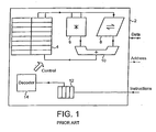
- This data processing system comprises a processor core including a register bank 4, a multiplier 6, a shifter 8, an adder 10, an instruction pipeline 12 and an instruction decoder 14. It will be understood by those skilled in this technical field that the processor core 2 will typically include many further circuit elements, which have been omitted from Figure 1 for the sake of clarity.
- the processor core 2 fetches program instructions to the instruction pipeline 12 wherein they are decoded by the instruction decoder 14 to generate control signals that act upon the register bank 4, the multiplier 6, the shifter 8 and the adder 10 as well as other circuit elements to control the desired data processing operations as specified by the program instruction being decoded.
- the processor core 2 is provided with a data bus, an address bus and an instruction bus.
- One type of processing operation that can be required is the generation of an address offset value.
- One example of this type of operation is the BL/BLX instruction which is present in the Thumb mode of operation of Thumb enabled processors produced by ARM Limited of Cambridge, England.
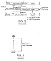
- Figure 2 of the accompanying drawings schematically illustrates such instructions. It will be seen that these instructions can be considered as two 16-bit instructions or one 32-bit instruction.
- the leading five bits (namely 11110) are decoded as indicating that a BL/BLX instruction is present with the remaining eleven bits within the first two bytes being an offset value, including a leading sign bit S, this being offset field 2.
- This offset value is then followed by a bit pattern 111t1 and a further eleven bits of offset, this being offset field 1.
- the "t" bit indicates to the instruction decoder 14 whether the instruction is a BL instruction or a BLX instruction.
- a BL instruction is a branch with link staying within the Thumb mode of operation.
- a BLX instruction is a branch with link combined with a switch to the ARM mode of operation.
- offset values illustrated in Figure 2 provide twenty two bits. This offset value is sign-extended as required and then added to the branch instruction's address. This offset value range is able to support branch jumps of plus or minus 4MB to 16-bit halfword-aligned targets.
- Figure 3 schematically illustrates the action of a BL instruction in jumping the program execution flow to a new point.
- the maximum jump that can be commanded is constrained by the maximum address offset value which may be specified.
- the present invention provides apparatus for processing data, said apparatus comprising:
- the invention recognises that some bits within the existing address offset generating instructions may be redundant in that they are not required to positively identify and accordingly decode the instruction concerned (e.g. once the first 16 bits of a BL/BLX have been identified the following 16 bits are constrained to be the second half of either a BL instruction or a BLX instruction) and accordingly those bits may be used to instead encode additional address offset information thereby extending the address offset range.
- the encoding used to represent the extra bits of the address offset value must be such that when legacy code is executed in which the extra bits have fixed values (the respective predetermined values), then those fixed values will be decoded in a way that generates the same offset value as was originally intended when the legacy software was written, i.e. appropriately sign extended. This is achieved by the encoding of the present technique as specified above. It will be appreciated that the fixed bits in the legacy code which are being reused to represent additional bits of address offset with the present technique could have had previously fixed values of either "0" or "1".
- a preferred encoding is one in which said respective predetermined values of said high order field bits P k are all equal to 1.
- said directly sign bit specified value of j is N-1. It is advantageous if the sign bit of the final offset can be obtained directly from the instruction encoding, without requiring an exclusive-(N)OR function to be evaluated. As an example, this may be advantageous because the sign bit of the final offset may need to be replicated, in which case putting the buffering delay in parallel with the exclusive-(N)OR delay rather than in series with it reduces critical paths. Another reason why it may be advantageous is that some branch prediction schemes pay attention to the direction of a branch instruction, and so may want to know the sign of the offset without knowing its exact value.
- D k is a predetermined value
- address offset generating instruction could have a variety of different forms and is not necessarily limited to branch instructions. However, the present invention is particularly well suited for use in branch instructions.
- preferred embodiments When using a branch instruction, preferred embodiments combine the branch target address offset with the current program address to generate a branch target address to which the program jumps.
- bits of the address offset value not being specified by the new technique also need to be specified within the address offset generating instruction. These could be encoded in a variety of different ways, but it is advantageously simple when these are directly specified by fields within the address offset generating instruction.
- the present invention provides a method of processing data, said method comprising the steps of:
- the present invention provides a computer program product including a computer program for controlling a computer to perform the steps of:
- the computer program product can take a wide variety of different forms, such as a storage medium or a download from a data connection or the like.
- the computer program concerned should include one or more address offset generating instructions utilizing the present technique.
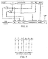
- Figure 5 schematically illustrates an address offset generating instruction (a new BL/BLX instruction in the ARM/Thumb type of system). Comparing this instruction with Figure 2 , it will be seen that the two bits adjacent to the "t" value have been reused to encode additional information regarding the address offset value in accordance with the logical expression shown in Figure 4 . Thus, the full address offset value is given by the legacy address offset fields together with the two additional bit values interpreted as described above.
- Figure 6 illustrates more directly how the address offset value can be derived from the address offset generating instruction of Figure 5 .
- the legacy address offset fields are taken directly and put in the same places as before.
- the two additional bit values encoding the additional address offset information namely P 1 and P 0 are combined with the sign bit S which is the most significant bit of the legacy offset value using respective logic gates as shown to generate the bits B N-2 and B N-3 of the extended address offset value.
- the sign bit S is used directly to provide B N-1 of the extended address offset value.
- the extended address offset value so produced is a 25-bit value (a LSB value of "0" is also incorporated in view of halfword (16-bit halfwords in this example) alignment).
- the 25-bit value is further sign extended to produce a 32-bit value to be combined with a 32-bit address value (e.g. as part of a branch operation).
- This combination may be by adding to the branch instruction's PC value, which is its address plus a constant offset (4 in Thumb/Wrist).
- Other processing operations and combinations of operations which give the same result are also encompassed within the present technique.
- an address offset range which was previously limited to plus or minus 4MB
- this may be extended to plus or minus 16MB, which is a significant advantage.
- This extended range is achieved in a manner which is backwards compatible with existing code.
- Figure 7 is a table illustrating a more general relationship between the high order field bits P 1 and P 0 , the sign bit of the offset S and the result three most significant bits B N-1 and B N-2 and B N-3 of the resulting offset value.
- this corresponds to the legacy encoding and so all three values B N-1 and B N-2 and B N-3 equal S.
- This leaves six other possible combinations of S, P 1 and P 0 which are subject to a one-to-one mapping to the remaining possible 3-bit combinations of B N-1 and B N-2 and B N-3 .
- One example of such a mapping is the one shown in Figures 4 and 6 .
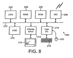
- FIG. 8 schematically illustrates a general purpose computer 200 which may implement program instructions in accordance with the above described techniques.
- the general purpose computer 200 includes a central processing unit 202, a random access memory 204, a read only memory 206, a network interface card 208, a hard disk drive 210, a display driver 212 and monitor 214 and a user input/output circuit 216 with a keyboard 218 and mouse 220 all connected via a common bus 222.
- the central processing unit 202 will execute computer program instructions that may be stored in one or more of the random access memory 204, the read only memory 206 and the hard disk drive 210 or dynamically downloaded via the network interface card 208.
- the results of the processing performed may be displayed to a user via the display driver 212 and the monitor 214.
- User inputs for controlling the operation of the general purpose computer 200 may be received via the user input output circuit 216 from the keyboard 218 or the mouse 220. It will be appreciated that the computer program could be written in a variety of different computer languages. The computer program may be stored and distributed on a recording medium or dynamically downloaded to the general purpose computer 200. When operating under control of an appropriate computer program, the general purpose computer 200 can perform the above described techniques and can be considered to form an apparatus for performing the above described technique.
- the architecture of the general purpose computer 200 could vary considerably and Figure 8 is only one example.
Landscapes
- Engineering & Computer Science (AREA)
- Software Systems (AREA)
- Theoretical Computer Science (AREA)
- Physics & Mathematics (AREA)
- General Engineering & Computer Science (AREA)
- General Physics & Mathematics (AREA)
- Executing Machine-Instructions (AREA)
Claims (26)
- Appareil (2) destiné à traiter des données, ledit appareil comprenant :un décodeur d'instructions (14) sensible à des instructions de programme pour commander des opérations de traitement de données ; et un circuit générateur de décalage d'adresse (4, 6, 8, 10) commandé par ledit décodeur d'instructions et ayant pour fonction de générer un décalage d'adresse à N bits ayant une valeur spécifiée par une instruction génératrice de décalage d'adresse contenant un bit S spécifiant le signe de la valeur de décalage ; caractérisé en ce que :ledit décalage d'adresse à N bits a des valeurs de bits Bi lorsqu'il est exprimé sous la forme d'un nombre en complément à deux, où (N-1)≥i≥Z et (N-1)>Z≥0, ladite instruction génératrice de décalage d'adresse contenant L bits d'extension de décalage Pk, où (N-Z)>L≥1 et L>k≥0, et ledit circuit générateur de décalage d'adresse peut être mis en fonctionnement de manière à ce que :(i) si la totalité desdits bits d'extension de décalage Pk ont des valeurs Dk prédéterminées respectives qui sont d'anciennes valeurs, alors les bits Bj dudit décalage d'adresse à N bits sont donnés par Bj = S pour toutes les valeurs de j telles que (N-1)≥j≥(N-L-1) ; et(ii) si l'un quelconque desdits bits d'extension de décalage Pk n'a pas ladite valeur Dk prédéterminée, alors les bits Bj dudit décalage d'adresse à N bits, où (N-1)≥j≥(N-L-1), sont donnés par une mise en correspondance biunivoque prédéterminée de combinaisons de valeurs desdits bits d'extension de décalage Pk et dudit bit S spécifiant le signe de la valeur de décalage vers des combinaisons de valeurs de Bj autres que les combinaisons Bj = 1 pour toutes les valeurs de j telles que (N-1)≥j≥(N-L-1) et que la combinaison Bj = 0 pour toutes les valeurs de j telles que (N-1)≥j≥(N-L-1).
- Appareil selon la revendication 1, dans lequel lesdites valeurs Dk prédéterminées sont toutes égales à 1.
- Appareil selon l'une quelconque des revendications 1 à 2, dans lequel ledit circuit générateur de décalage d'adresse peut être mis en fonctionnement pour générer des valeurs de bits Bj dudit décalage d'adresse à N bits, chaque valeur de bit Bj ayant une valeur respective prédéterminée parmi :Bj = S pour une valeur de j à bit de signe directement spécifié ;Bj = S OU-EX Pk(j) OU-EX Dk(j), où k(j) est une mise en correspondance biunivoque d'indices des valeurs de j, à l'exclusion de ladite valeur de j à bit de signe directement spécifié, vers des valeurs de k.
- Appareil selon la revendication 3, dans lequel ladite valeur de j à bit de signe directement spécifié est N-1.
- Appareil selon l'une quelconque des revendications précédentes, dans lequel ladite instruction génératrice de décalage d'adresse est une instruction de branchement et ledit décalage d'adresse à N bits est un décalage d'adresse cible de branchement à N bits.
- Appareil selon la revendication 5, dans lequel ledit décalage d'adresse cible de branchement à N bits est combiné à une adresse de programme de ladite instruction de branchement pour générer une adresse cible de branchement.
- Appareil selon l'une quelconque des revendications précédentes, dans lequel ledit décalage d'adresse à N bits est en outre soumis à une extension de signe par ladite instruction génératrice de décalage d'adresse avant l'utilisation.
- Appareil selon l'une quelconque des revendications précédentes, dans lequel L = 2.
- Appareil selon l'une quelconque des revendications précédentes, dans lequel N = 25.
- Appareil selon l'une quelconque des revendications précédentes, dans lequel Z est soit 1 soit 2.
- Appareil selon l'une quelconque des revendications précédentes, dans lequel les valeurs de bits BN-2-L à BZ sont directement spécifiées dans ladite instruction génératrice de décalage d'adresse.
- Procédé de traitement de données, ledit procédé comprenant les étapes consistant à :commander des opérations de traitement des données en utilisant un décodeur d'instructions (14) sensible à des instructions de programmes ; etgénérer un décalage d'adresse à N bits ayant une valeur spécifiée par une instruction génératrice de décalage d'adresse contenant un bit S spécifiant le signe de la valeur de décalage en utilisant un circuit générateur de décalage d'adresse (4, 6, 8, 10) commandé par ledit décodeur d'instructions ; caractérisé en ce que :ledit décalage d'adresse à N bits a des valeurs de bits Bi lorsqu'il est exprimé sous la forme d'un nombre en complément à deux, où (N-1)≥i≥Z et (N-1)>Z≥0, ladite instruction génératrice de décalage d'adresse contient L bits d'extension de décalage Pk, où (N-Z)>L≥1 et L>k≥0, et ledit circuit générateur de décalage d'adresse peut être mis en fonctionnement de manière à ce que :(i) si la totalité desdits bits d'extension de décalage Pk ont des valeurs Dk prédéterminées respectives qui sont d'anciennes valeurs, alors les bits Bj dudit décalage d'adresse à N bits sont donnés par Bj = S pour toutes les valeurs de j telles que (N-1)≥j≥(N-L-1) ; et(ii) si l'un quelconque desdits bits d'extension de décalage Pk n'a pas ladite valeur Dk prédéterminée, alors les bits Bj dudit décalage d'adresse à N bits, où (N-1)≥j≥(N-L-1), sont donnés par une mise en correspondance biunivoque prédéterminée de combinaisons de valeurs desdits bits d'extension de décalage Pk et dudit bit S spécifiant le signe de la valeur de décalage vers des combinaisons de valeurs de Bj autres que les combinaisons Bj = 1 pour toutes les valeurs de j telles que (N-1)≥j≥(N-L-1) et que la combinaison Bj = 0 pour toutes les valeurs de j telles que (N-1)≥j≥(N-L-1).
- Procédé selon la revendication 12, dans lequel lesdites valeurs Dk prédéterminées sont toutes égales à 1.
- Procédé selon l'une quelconque des revendications 12 et 13, dans lequel ledit circuit générateur de décalage d'adresse peut être mis en fonctionnement pour générer des valeurs de bits Bj dudit décalage d'adresse à N bits, chaque valeur de bit Bj ayant une valeur respective prédéterminée parmi :Bj = S pour une valeur de j à bit de signe directement spécifié ;Bj = S OU-EX Pk(j) OU-EX Dk(j), où k(j) est une mise en correspondance biunivoque d'indices des valeurs de j, à l'exclusion de ladite valeur de j à bit de signe directement spécifié, vers des valeurs de k.
- Procédé selon la revendication 14, dans lequel ladite valeur de j à bit de signe directement spécifié est N-1.
- Procédé selon l'une quelconque des revendications 12 à 15, dans lequel ladite instruction génératrice de décalage d'adresse est une instruction de branchement et ledit décalage d'adresse à N bits est un décalage d'adresse cible de branchement à N bits.
- Procédé selon la revendication 16, dans lequel ledit décalage d'adresse cible de branchement à N bits est combiné à une adresse de programme de ladite instruction de branchement pour générer une adresse cible de branchement.
- Procédé selon l'une quelconque des revendications 12 à 17, dans lequel ledit décalage d'adresse à N bits est en outre soumis à une extension de signe par ladite instruction génératrice de décalage d'adresse avant l'utilisation.
- Procédé selon l'une quelconque des revendications 12 à 18, dans lequel L = 2.
- Procédé selon l'une quelconque des revendications 12 à 19, dans lequel N = 25.
- Procédé selon l'une quelconque des revendications 12 à 20, dans lequel Z est soit 1 soit 2.
- Procédé selon l'une quelconque des revendications 12 à 21, dans lequel les valeurs de bits BN-2-L à BZ sont directement spécifiées dans ladite instruction génératrice de décalage d'adresse.
- Produit de programme informatique comprenant un programme informatique destiné à commander un ordinateur afin qu'il mette en oeuvre les étapes consistant à :commander des opérations de traitement de données en utilisant un décodeur d'instructions (14) sensible à des instructions de programmes ; etgénérer un décalage d'adresse à N bits ayant une valeur spécifiée par une instruction génératrice de décalage d'adresse contenant un bit S spécifiant le signe de la valeur de décalage en utilisant un circuit générateur de décalage d'adresse (4, 6, 8, 10) commandé par ledit décodeur d'instructions ; caractérisé en ce que :ledit décalage d'adresse à N bits a des valeurs de bits Bi lorsqu'il est exprimé sous la forme d'un nombre en complément à deux, où (N-1)≥1≥Z et (N-1)>Z≥0, ladite instruction génératrice de décalage d'adresse contient L bits d'extension de décalage Pk, où (N-Z)>L≥1 et L>k≥0, et ledit circuit générateur de décalage d'adresse peut être mis en fonctionnement de manière à ce que :(i) si la totalité desdits bits d'extension de décalage Pk ont des valeurs Dk prédéterminées respectives qui sont d'anciennes valeurs, alors les bits Bj dudit décalage d'adresse à N bits sont donnés par Bj = S pour toutes les valeurs de j telles que (N-1)≥j≥(N-L-1) ; et(ii) si l'un quelconque desdits bits d'extension de décalage Pk n'a pas ladite valeur Dk prédéterminée, alors les bits Bj dudit décalage d'adresse à N bits, où (N-1)≥j≥(N-L-1), sont donnés par une mise en correspondance biunivoque prédéterminée de combinaisons de valeurs desdits bits d'extension de décalage Pk et dudit bit S spécifiant le signe de la valeur de décalage vers des combinaisons de valeurs de Bj autres que les combinaisons Bj = 1 pour toutes les valeurs de j telles que (N-1)≥j≥(N-L-1) et que la combinaison Bj = 0 pour toutes les valeurs de j telles que (N-1)≥j≥(N-L-1).
- Produit de programme informatique selon la revendication 23, dans lequel lesdites valeurs Dk prédéterminées sont toutes égales à 1.
- Produit de programme informatique selon l'une quelconque des revendications 23 et 24, dans lequel ledit circuit générateur de décalage d'adresse peut être mis en fonctionnement pour générer des valeurs de bits Bj dudit décalage d'adresse à N bits, chaque valeur de bit Bj ayant une valeur respective prédéterminée parmi :Bj = S pour une valeur de j à bit de signe directement spécifié ;Bj = S OU-EX Pk(j) OU-EX Dk(j), où k(j) est une mise en correspondance biunivoque d'indices des valeurs de j, à l'exclusion de ladite valeur de j à bit de signe directement spécifié, vers des valeurs de k.
- Produit de programme informatique selon la revendication 25, dans lequel ladite valeur de j à bit de signe directement spécifié est N-1.
Applications Claiming Priority (2)
| Application Number | Priority Date | Filing Date | Title |
|---|---|---|---|
| GB0313510A GB2402757B (en) | 2003-06-11 | 2003-06-11 | Address offset generation within a data processing system |
| PCT/GB2003/005680 WO2004111837A2 (fr) | 2003-06-11 | 2003-12-30 | Decalage d'adresse dans un systeme de traitement de donnees |
Publications (3)
| Publication Number | Publication Date |
|---|---|
| EP1631903A2 EP1631903A2 (fr) | 2006-03-08 |
| EP1631903B1 true EP1631903B1 (fr) | 2012-12-19 |
| EP1631903B8 EP1631903B8 (fr) | 2013-03-06 |
Family
ID=27589902
Family Applications (1)
| Application Number | Title | Priority Date | Filing Date |
|---|---|---|---|
| EP03782716A Expired - Lifetime EP1631903B8 (fr) | 2003-06-11 | 2003-12-30 | Generation de decalage d'adresse dans un systeme de traitement de donnees |
Country Status (11)
| Country | Link |
|---|---|
| US (1) | US7120779B2 (fr) |
| EP (1) | EP1631903B8 (fr) |
| JP (1) | JP3917636B2 (fr) |
| KR (1) | KR100951331B1 (fr) |
| CN (1) | CN100375012C (fr) |
| AU (1) | AU2003290355A1 (fr) |
| GB (1) | GB2402757B (fr) |
| MY (1) | MY134215A (fr) |
| RU (1) | RU2006100297A (fr) |
| TW (1) | TWI290288B (fr) |
| WO (1) | WO2004111837A2 (fr) |
Families Citing this family (7)
| Publication number | Priority date | Publication date | Assignee | Title |
|---|---|---|---|---|
| US7769983B2 (en) * | 2005-05-18 | 2010-08-03 | Qualcomm Incorporated | Caching instructions for a multiple-state processor |
| GB2475653B (en) | 2007-03-12 | 2011-07-13 | Advanced Risc Mach Ltd | Select and insert instructions within data processing systems |
| US7711927B2 (en) * | 2007-03-14 | 2010-05-04 | Qualcomm Incorporated | System, method and software to preload instructions from an instruction set other than one currently executing |
| US20110082999A1 (en) * | 2009-10-07 | 2011-04-07 | Andes Technology Corporation | Data processing engine with integrated data endianness control mechanism |
| GB2488980B (en) * | 2011-03-07 | 2020-02-19 | Advanced Risc Mach Ltd | Address generation in a data processing apparatus |
| US20160132332A1 (en) * | 2013-06-18 | 2016-05-12 | Freescale Semiconductor, Inc. | Signal processing device and method of performing a bit-expand operation |
| US20240143361A1 (en) * | 2022-10-01 | 2024-05-02 | Intel Corporation | Apparatus and method for managing deprecated instruction set architecture (isa) features |
Family Cites Families (12)
| Publication number | Priority date | Publication date | Assignee | Title |
|---|---|---|---|---|
| US4203157A (en) * | 1978-09-05 | 1980-05-13 | Motorola, Inc. | Carry anticipator circuit and method |
| US4935867A (en) * | 1986-03-04 | 1990-06-19 | Advanced Micro Devices, Inc. | Signal processor memory management unit with indirect addressing using selectable offsets and modulo values for indexed address calculations |
| US5386534A (en) * | 1992-10-27 | 1995-01-31 | Motorola, Inc. | Data processing system for generating symmetrical range of addresses of instructing-address-value with the use of inverting sign value |
| US20010025337A1 (en) * | 1996-06-10 | 2001-09-27 | Frank Worrell | Microprocessor including a mode detector for setting compression mode |
| US6049863A (en) | 1996-07-24 | 2000-04-11 | Advanced Micro Devices, Inc. | Predecoding technique for indicating locations of opcode bytes in variable byte-length instructions within a superscalar microprocessor |
| US6237087B1 (en) * | 1998-09-30 | 2001-05-22 | Intel Corporation | Method and apparatus for speeding sequential access of a set-associative cache |
| US6691305B1 (en) * | 1999-11-10 | 2004-02-10 | Nec Corporation | Object code compression using different schemes for different instruction types |
| US7051189B2 (en) * | 2000-03-15 | 2006-05-23 | Arc International | Method and apparatus for processor code optimization using code compression |
| WO2003065165A2 (fr) * | 2002-01-31 | 2003-08-07 | Arc International | Processeur de donnees configurable presentant une architecture de jeu d'instructions a longueur variable |
| US6948053B2 (en) * | 2002-02-25 | 2005-09-20 | International Business Machines Corporation | Efficiently calculating a branch target address |
| US20040049657A1 (en) * | 2002-09-10 | 2004-03-11 | Kling Ralph M. | Extended register space apparatus and methods for processors |
| US20050114633A1 (en) * | 2003-11-25 | 2005-05-26 | Palat Manoj N. | Method and system for executing data-relative code within a non data-relative environment |
-
2003
- 2003-06-11 GB GB0313510A patent/GB2402757B/en not_active Expired - Lifetime
- 2003-12-30 KR KR1020057023535A patent/KR100951331B1/ko not_active Expired - Lifetime
- 2003-12-30 AU AU2003290355A patent/AU2003290355A1/en not_active Abandoned
- 2003-12-30 RU RU2006100297/09A patent/RU2006100297A/ru not_active Application Discontinuation
- 2003-12-30 WO PCT/GB2003/005680 patent/WO2004111837A2/fr not_active Ceased
- 2003-12-30 EP EP03782716A patent/EP1631903B8/fr not_active Expired - Lifetime
- 2003-12-30 JP JP2005500706A patent/JP3917636B2/ja not_active Expired - Lifetime
- 2003-12-30 CN CNB2003801103414A patent/CN100375012C/zh not_active Expired - Lifetime
-
2004
- 2004-01-28 US US10/765,092 patent/US7120779B2/en not_active Expired - Lifetime
- 2004-02-09 TW TW093102968A patent/TWI290288B/zh not_active IP Right Cessation
- 2004-02-10 MY MYPI20040388A patent/MY134215A/en unknown
Also Published As
| Publication number | Publication date |
|---|---|
| GB2402757B (en) | 2005-11-02 |
| US20040255094A1 (en) | 2004-12-16 |
| WO2004111837A3 (fr) | 2007-03-29 |
| KR100951331B1 (ko) | 2010-04-08 |
| TW200428226A (en) | 2004-12-16 |
| US7120779B2 (en) | 2006-10-10 |
| GB0313510D0 (en) | 2003-07-16 |
| AU2003290355A8 (en) | 2005-01-04 |
| GB2402757A (en) | 2004-12-15 |
| CN100375012C (zh) | 2008-03-12 |
| WO2004111837A2 (fr) | 2004-12-23 |
| AU2003290355A1 (en) | 2005-01-04 |
| RU2006100297A (ru) | 2006-06-10 |
| KR20060021349A (ko) | 2006-03-07 |
| EP1631903B8 (fr) | 2013-03-06 |
| CN1788252A (zh) | 2006-06-14 |
| JP2006527419A (ja) | 2006-11-30 |
| TWI290288B (en) | 2007-11-21 |
| JP3917636B2 (ja) | 2007-05-23 |
| EP1631903A2 (fr) | 2006-03-08 |
| MY134215A (en) | 2007-11-30 |
Similar Documents
| Publication | Publication Date | Title |
|---|---|---|
| EP0083209B1 (fr) | Microprocesseur pouvant traiter des instructions de différents types | |
| US7287152B2 (en) | Conditional execution per lane | |
| JP3790619B2 (ja) | 正値化処理及び飽和演算処理からなる丸め処理を好適に行うことができるプロセッサ | |
| US7447871B2 (en) | Data access program instruction encoding | |
| CN1332407A (zh) | 用以执行多重指令组的数据处理装置 | |
| JP2009026106A (ja) | 命令コード圧縮方法と命令フェッチ回路 | |
| JPS6029126B2 (ja) | デ−タ処理装置 | |
| JPH0470662B2 (fr) | ||
| JPH04233640A (ja) | メモリ拡張スキームを切り替える疑似直線バンクを有するマイクロコントローラ | |
| KR100971626B1 (ko) | 다수의 명령어 세트를 갖는 데이터 처리 장치 내에서의명령어 부호화 | |
| EP1631903B1 (fr) | Generation de decalage d'adresse dans un systeme de traitement de donnees | |
| US7647368B2 (en) | Data processing apparatus and method for performing data processing operations on floating point data elements | |
| US20040024992A1 (en) | Decoding method for a multi-length-mode instruction set | |
| US6922773B2 (en) | System and method for encoding constant operands in a wide issue processor | |
| US20050015574A1 (en) | Processor and method capable of executing instruction sets with different lengths | |
| US5721894A (en) | Jump prediction | |
| US6996702B2 (en) | Processing unit with cross-coupled ALUs/accumulators and input data feedback structure including constant generator and bypass to reduce memory contention | |
| JP3252029B2 (ja) | 符号化装置及び符号化方法 | |
| IE56443B1 (en) | Microprogram control | |
| CN113805942A (zh) | 处理器核、处理器及指令处理方法 | |
| JP2006251940A (ja) | マイクロプログラム制御装置 | |
| JPH07146791A (ja) | 命令デコード装置 |
Legal Events
| Date | Code | Title | Description |
|---|---|---|---|
| PUAI | Public reference made under article 153(3) epc to a published international application that has entered the european phase |
Free format text: ORIGINAL CODE: 0009012 |
|
| 17P | Request for examination filed |
Effective date: 20051018 |
|
| AK | Designated contracting states |
Kind code of ref document: A2 Designated state(s): AT BE BG CH CY CZ DE DK EE ES FI FR GB GR HU IE IT LI LU MC NL PT RO SE SI SK TR |
|
| AX | Request for extension of the european patent |
Extension state: AL LT LV MK |
|
| DAX | Request for extension of the european patent (deleted) | ||
| RBV | Designated contracting states (corrected) |
Designated state(s): DE FR GB IT NL |
|
| PUAK | Availability of information related to the publication of the international search report |
Free format text: ORIGINAL CODE: 0009015 |
|
| 17Q | First examination report despatched |
Effective date: 20080722 |
|
| RIC1 | Information provided on ipc code assigned before grant |
Ipc: G06F 9/32 20060101AFI20120531BHEP Ipc: G06F 9/318 20060101ALI20120531BHEP Ipc: G06F 9/30 20060101ALI20120531BHEP Ipc: G06F 9/34 20060101ALI20120531BHEP |
|
| GRAP | Despatch of communication of intention to grant a patent |
Free format text: ORIGINAL CODE: EPIDOSNIGR1 |
|
| GRAS | Grant fee paid |
Free format text: ORIGINAL CODE: EPIDOSNIGR3 |
|
| GRAA | (expected) grant |
Free format text: ORIGINAL CODE: 0009210 |
|
| AK | Designated contracting states |
Kind code of ref document: B1 Designated state(s): DE FR GB IT NL |
|
| REG | Reference to a national code |
Ref country code: GB Ref legal event code: FG4D |
|
| RBV | Designated contracting states (corrected) |
Designated state(s): DE FR IT NL |
|
| REG | Reference to a national code |
Ref country code: DE Ref legal event code: R096 Ref document number: 60342912 Country of ref document: DE Effective date: 20130221 |
|
| REG | Reference to a national code |
Ref country code: NL Ref legal event code: VDEP Effective date: 20121219 |
|
| PG25 | Lapsed in a contracting state [announced via postgrant information from national office to epo] |
Ref country code: NL Free format text: LAPSE BECAUSE OF FAILURE TO SUBMIT A TRANSLATION OF THE DESCRIPTION OR TO PAY THE FEE WITHIN THE PRESCRIBED TIME-LIMIT Effective date: 20121219 |
|
| PLBE | No opposition filed within time limit |
Free format text: ORIGINAL CODE: 0009261 |
|
| STAA | Information on the status of an ep patent application or granted ep patent |
Free format text: STATUS: NO OPPOSITION FILED WITHIN TIME LIMIT |
|
| 26N | No opposition filed |
Effective date: 20130920 |
|
| PG25 | Lapsed in a contracting state [announced via postgrant information from national office to epo] |
Ref country code: IT Free format text: LAPSE BECAUSE OF FAILURE TO SUBMIT A TRANSLATION OF THE DESCRIPTION OR TO PAY THE FEE WITHIN THE PRESCRIBED TIME-LIMIT Effective date: 20121219 |
|
| REG | Reference to a national code |
Ref country code: DE Ref legal event code: R097 Ref document number: 60342912 Country of ref document: DE Effective date: 20130920 |
|
| REG | Reference to a national code |
Ref country code: FR Ref legal event code: PLFP Year of fee payment: 13 |
|
| REG | Reference to a national code |
Ref country code: FR Ref legal event code: PLFP Year of fee payment: 14 |
|
| REG | Reference to a national code |
Ref country code: FR Ref legal event code: PLFP Year of fee payment: 15 |
|
| REG | Reference to a national code |
Ref country code: DE Ref legal event code: R082 Ref document number: 60342912 Country of ref document: DE Representative=s name: D YOUNG & CO LLP, DE |
|
| PGFP | Annual fee paid to national office [announced via postgrant information from national office to epo] |
Ref country code: FR Payment date: 20221122 Year of fee payment: 20 Ref country code: DE Payment date: 20221122 Year of fee payment: 20 |
|
| P01 | Opt-out of the competence of the unified patent court (upc) registered |
Effective date: 20230429 |
|
| REG | Reference to a national code |
Ref country code: DE Ref legal event code: R071 Ref document number: 60342912 Country of ref document: DE |