EP1630869A2 - Active matrix substrate, method of manufacturing active matrix substrate, electro-optical device, and electronic apparatus - Google Patents
Active matrix substrate, method of manufacturing active matrix substrate, electro-optical device, and electronic apparatus Download PDFInfo
- Publication number
- EP1630869A2 EP1630869A2 EP05018371A EP05018371A EP1630869A2 EP 1630869 A2 EP1630869 A2 EP 1630869A2 EP 05018371 A EP05018371 A EP 05018371A EP 05018371 A EP05018371 A EP 05018371A EP 1630869 A2 EP1630869 A2 EP 1630869A2
- Authority
- EP
- European Patent Office
- Prior art keywords
- wires
- active matrix
- substrate
- matrix substrate
- pixel electrodes
- Prior art date
- Legal status (The legal status is an assumption and is not a legal conclusion. Google has not performed a legal analysis and makes no representation as to the accuracy of the status listed.)
- Withdrawn
Links
- 239000000758 substrate Substances 0.000 title claims abstract description 103
- 239000011159 matrix material Substances 0.000 title claims abstract description 41
- 238000004519 manufacturing process Methods 0.000 title claims description 10
- 238000000034 method Methods 0.000 claims description 80
- 239000007788 liquid Substances 0.000 claims description 29
- 239000010408 film Substances 0.000 description 54
- 239000000463 material Substances 0.000 description 35
- 230000008569 process Effects 0.000 description 35
- 239000010410 layer Substances 0.000 description 30
- 239000004973 liquid crystal related substance Substances 0.000 description 24
- 239000004020 conductor Substances 0.000 description 19
- 239000002245 particle Substances 0.000 description 17
- 238000010586 diagram Methods 0.000 description 14
- 239000003990 capacitor Substances 0.000 description 12
- 239000004065 semiconductor Substances 0.000 description 12
- 239000002612 dispersion medium Substances 0.000 description 10
- 239000011344 liquid material Substances 0.000 description 9
- 239000002184 metal Substances 0.000 description 8
- 229910052751 metal Inorganic materials 0.000 description 8
- 230000001681 protective effect Effects 0.000 description 8
- 239000006185 dispersion Substances 0.000 description 7
- 238000001035 drying Methods 0.000 description 7
- 239000003795 chemical substances by application Substances 0.000 description 6
- 238000005530 etching Methods 0.000 description 6
- 230000007246 mechanism Effects 0.000 description 6
- 238000004140 cleaning Methods 0.000 description 5
- 238000007789 sealing Methods 0.000 description 5
- 239000010409 thin film Substances 0.000 description 5
- 239000011135 tin Substances 0.000 description 5
- XTHFKEDIFFGKHM-UHFFFAOYSA-N Dimethoxyethane Chemical compound COCCOC XTHFKEDIFFGKHM-UHFFFAOYSA-N 0.000 description 4
- PXHVJJICTQNCMI-UHFFFAOYSA-N Nickel Chemical compound [Ni] PXHVJJICTQNCMI-UHFFFAOYSA-N 0.000 description 4
- -1 acryl Chemical group 0.000 description 4
- 238000006243 chemical reaction Methods 0.000 description 4
- 239000011521 glass Substances 0.000 description 4
- 238000000206 photolithography Methods 0.000 description 4
- LFQSCWFLJHTTHZ-UHFFFAOYSA-N Ethanol Chemical compound CCO LFQSCWFLJHTTHZ-UHFFFAOYSA-N 0.000 description 3
- YCKRFDGAMUMZLT-UHFFFAOYSA-N Fluorine atom Chemical compound [F] YCKRFDGAMUMZLT-UHFFFAOYSA-N 0.000 description 3
- OKKJLVBELUTLKV-UHFFFAOYSA-N Methanol Chemical compound OC OKKJLVBELUTLKV-UHFFFAOYSA-N 0.000 description 3
- ZMXDDKWLCZADIW-UHFFFAOYSA-N N,N-Dimethylformamide Chemical compound CN(C)C=O ZMXDDKWLCZADIW-UHFFFAOYSA-N 0.000 description 3
- IMNFDUFMRHMDMM-UHFFFAOYSA-N N-Heptane Chemical compound CCCCCCC IMNFDUFMRHMDMM-UHFFFAOYSA-N 0.000 description 3
- YXFVVABEGXRONW-UHFFFAOYSA-N Toluene Chemical compound CC1=CC=CC=C1 YXFVVABEGXRONW-UHFFFAOYSA-N 0.000 description 3
- 230000015572 biosynthetic process Effects 0.000 description 3
- 230000001413 cellular effect Effects 0.000 description 3
- 239000011248 coating agent Substances 0.000 description 3
- 150000001875 compounds Chemical class 0.000 description 3
- 229910052731 fluorine Inorganic materials 0.000 description 3
- 239000011737 fluorine Substances 0.000 description 3
- 238000010438 heat treatment Methods 0.000 description 3
- 150000002430 hydrocarbons Chemical class 0.000 description 3
- 230000010365 information processing Effects 0.000 description 3
- 239000011368 organic material Substances 0.000 description 3
- 229920005989 resin Polymers 0.000 description 3
- 239000011347 resin Substances 0.000 description 3
- 230000004044 response Effects 0.000 description 3
- 239000000243 solution Substances 0.000 description 3
- XLYOFNOQVPJJNP-UHFFFAOYSA-N water Substances O XLYOFNOQVPJJNP-UHFFFAOYSA-N 0.000 description 3
- RYHBNJHYFVUHQT-UHFFFAOYSA-N 1,4-Dioxane Chemical compound C1COCCO1 RYHBNJHYFVUHQT-UHFFFAOYSA-N 0.000 description 2
- YBYIRNPNPLQARY-UHFFFAOYSA-N 1H-indene Chemical compound C1=CC=C2CC=CC2=C1 YBYIRNPNPLQARY-UHFFFAOYSA-N 0.000 description 2
- YEJRWHAVMIAJKC-UHFFFAOYSA-N 4-Butyrolactone Chemical compound O=C1CCCO1 YEJRWHAVMIAJKC-UHFFFAOYSA-N 0.000 description 2
- RYGMFSIKBFXOCR-UHFFFAOYSA-N Copper Chemical compound [Cu] RYGMFSIKBFXOCR-UHFFFAOYSA-N 0.000 description 2
- RTZKZFJDLAIYFH-UHFFFAOYSA-N Diethyl ether Chemical compound CCOCC RTZKZFJDLAIYFH-UHFFFAOYSA-N 0.000 description 2
- IAZDPXIOMUYVGZ-UHFFFAOYSA-N Dimethylsulphoxide Chemical compound CS(C)=O IAZDPXIOMUYVGZ-UHFFFAOYSA-N 0.000 description 2
- 229920000877 Melamine resin Polymers 0.000 description 2
- 239000004640 Melamine resin Substances 0.000 description 2
- LRHPLDYGYMQRHN-UHFFFAOYSA-N N-Butanol Chemical compound CCCCO LRHPLDYGYMQRHN-UHFFFAOYSA-N 0.000 description 2
- 229910052581 Si3N4 Inorganic materials 0.000 description 2
- XUIMIQQOPSSXEZ-UHFFFAOYSA-N Silicon Chemical compound [Si] XUIMIQQOPSSXEZ-UHFFFAOYSA-N 0.000 description 2
- 150000001298 alcohols Chemical class 0.000 description 2
- 238000005229 chemical vapour deposition Methods 0.000 description 2
- 229910052802 copper Inorganic materials 0.000 description 2
- 239000010949 copper Substances 0.000 description 2
- JHIVVAPYMSGYDF-UHFFFAOYSA-N cyclohexanone Chemical compound O=C1CCCCC1 JHIVVAPYMSGYDF-UHFFFAOYSA-N 0.000 description 2
- NNBZCPXTIHJBJL-UHFFFAOYSA-N decalin Chemical compound C1CCCC2CCCCC21 NNBZCPXTIHJBJL-UHFFFAOYSA-N 0.000 description 2
- DIOQZVSQGTUSAI-UHFFFAOYSA-N decane Chemical compound CCCCCCCCCC DIOQZVSQGTUSAI-UHFFFAOYSA-N 0.000 description 2
- SBZXBUIDTXKZTM-UHFFFAOYSA-N diglyme Chemical compound COCCOCCOC SBZXBUIDTXKZTM-UHFFFAOYSA-N 0.000 description 2
- SNRUBQQJIBEYMU-UHFFFAOYSA-N dodecane Chemical compound CCCCCCCCCCCC SNRUBQQJIBEYMU-UHFFFAOYSA-N 0.000 description 2
- SQNZJJAZBFDUTD-UHFFFAOYSA-N durene Chemical compound CC1=CC(C)=C(C)C=C1C SQNZJJAZBFDUTD-UHFFFAOYSA-N 0.000 description 2
- 238000005401 electroluminescence Methods 0.000 description 2
- 150000002170 ethers Chemical class 0.000 description 2
- 239000012530 fluid Substances 0.000 description 2
- 230000006872 improvement Effects 0.000 description 2
- XMGQYMWWDOXHJM-UHFFFAOYSA-N limonene Chemical compound CC(=C)C1CCC(C)=CC1 XMGQYMWWDOXHJM-UHFFFAOYSA-N 0.000 description 2
- 230000005499 meniscus Effects 0.000 description 2
- 239000000203 mixture Substances 0.000 description 2
- 229910052759 nickel Inorganic materials 0.000 description 2
- TVMXDCGIABBOFY-UHFFFAOYSA-N octane Chemical compound CCCCCCCC TVMXDCGIABBOFY-UHFFFAOYSA-N 0.000 description 2
- 230000002093 peripheral effect Effects 0.000 description 2
- 229920001721 polyimide Polymers 0.000 description 2
- 239000009719 polyimide resin Substances 0.000 description 2
- 229920005672 polyolefin resin Polymers 0.000 description 2
- 238000003825 pressing Methods 0.000 description 2
- 238000000926 separation method Methods 0.000 description 2
- 229910052710 silicon Inorganic materials 0.000 description 2
- 239000010703 silicon Substances 0.000 description 2
- HQVNEWCFYHHQES-UHFFFAOYSA-N silicon nitride Chemical compound N12[Si]34N5[Si]62N3[Si]51N64 HQVNEWCFYHHQES-UHFFFAOYSA-N 0.000 description 2
- 229910052709 silver Inorganic materials 0.000 description 2
- 239000004332 silver Substances 0.000 description 2
- NDVLTYZPCACLMA-UHFFFAOYSA-N silver oxide Chemical compound [O-2].[Ag+].[Ag+] NDVLTYZPCACLMA-UHFFFAOYSA-N 0.000 description 2
- 239000002904 solvent Substances 0.000 description 2
- 238000003860 storage Methods 0.000 description 2
- BGHCVCJVXZWKCC-UHFFFAOYSA-N tetradecane Chemical compound CCCCCCCCCCCCCC BGHCVCJVXZWKCC-UHFFFAOYSA-N 0.000 description 2
- LZDKZFUFMNSQCJ-UHFFFAOYSA-N 1,2-diethoxyethane Chemical compound CCOCCOCC LZDKZFUFMNSQCJ-UHFFFAOYSA-N 0.000 description 1
- RRQYJINTUHWNHW-UHFFFAOYSA-N 1-ethoxy-2-(2-ethoxyethoxy)ethane Chemical compound CCOCCOCCOCC RRQYJINTUHWNHW-UHFFFAOYSA-N 0.000 description 1
- CNJRPYFBORAQAU-UHFFFAOYSA-N 1-ethoxy-2-(2-methoxyethoxy)ethane Chemical compound CCOCCOCCOC CNJRPYFBORAQAU-UHFFFAOYSA-N 0.000 description 1
- CAQYAZNFWDDMIT-UHFFFAOYSA-N 1-ethoxy-2-methoxyethane Chemical compound CCOCCOC CAQYAZNFWDDMIT-UHFFFAOYSA-N 0.000 description 1
- CTQNGGLPUBDAKN-UHFFFAOYSA-N O-Xylene Chemical compound CC1=CC=CC=C1C CTQNGGLPUBDAKN-UHFFFAOYSA-N 0.000 description 1
- VYPSYNLAJGMNEJ-UHFFFAOYSA-N Silicium dioxide Chemical compound O=[Si]=O VYPSYNLAJGMNEJ-UHFFFAOYSA-N 0.000 description 1
- BQCADISMDOOEFD-UHFFFAOYSA-N Silver Chemical compound [Ag] BQCADISMDOOEFD-UHFFFAOYSA-N 0.000 description 1
- ATJFFYVFTNAWJD-UHFFFAOYSA-N Tin Chemical compound [Sn] ATJFFYVFTNAWJD-UHFFFAOYSA-N 0.000 description 1
- 229910021417 amorphous silicon Inorganic materials 0.000 description 1
- 238000000137 annealing Methods 0.000 description 1
- 230000008901 benefit Effects 0.000 description 1
- 238000009835 boiling Methods 0.000 description 1
- 239000003086 colorant Substances 0.000 description 1
- 229920001940 conductive polymer Polymers 0.000 description 1
- HHNHBFLGXIUXCM-GFCCVEGCSA-N cyclohexylbenzene Chemical compound [CH]1CCCC[C@@H]1C1=CC=CC=C1 HHNHBFLGXIUXCM-GFCCVEGCSA-N 0.000 description 1
- 229930007927 cymene Natural products 0.000 description 1
- 230000003247 decreasing effect Effects 0.000 description 1
- 238000000151 deposition Methods 0.000 description 1
- 230000008021 deposition Effects 0.000 description 1
- 229940019778 diethylene glycol diethyl ether Drugs 0.000 description 1
- 230000005684 electric field Effects 0.000 description 1
- 150000002148 esters Chemical class 0.000 description 1
- 230000001747 exhibiting effect Effects 0.000 description 1
- PCHJSUWPFVWCPO-UHFFFAOYSA-N gold Chemical compound [Au] PCHJSUWPFVWCPO-UHFFFAOYSA-N 0.000 description 1
- 229910052737 gold Inorganic materials 0.000 description 1
- 239000010931 gold Substances 0.000 description 1
- AMGQUBHHOARCQH-UHFFFAOYSA-N indium;oxotin Chemical compound [In].[Sn]=O AMGQUBHHOARCQH-UHFFFAOYSA-N 0.000 description 1
- 238000002347 injection Methods 0.000 description 1
- 239000007924 injection Substances 0.000 description 1
- 150000002576 ketones Chemical class 0.000 description 1
- 239000011133 lead Substances 0.000 description 1
- 239000002923 metal particle Substances 0.000 description 1
- 230000005012 migration Effects 0.000 description 1
- 238000013508 migration Methods 0.000 description 1
- 239000002105 nanoparticle Substances 0.000 description 1
- 150000002894 organic compounds Chemical class 0.000 description 1
- 230000003647 oxidation Effects 0.000 description 1
- 238000007254 oxidation reaction Methods 0.000 description 1
- HFPZCAJZSCWRBC-UHFFFAOYSA-N p-cymene Chemical compound CC(C)C1=CC=C(C)C=C1 HFPZCAJZSCWRBC-UHFFFAOYSA-N 0.000 description 1
- 238000000059 patterning Methods 0.000 description 1
- 238000000016 photochemical curing Methods 0.000 description 1
- 238000005268 plasma chemical vapour deposition Methods 0.000 description 1
- 239000002985 plastic film Substances 0.000 description 1
- 229920006255 plastic film Polymers 0.000 description 1
- 229920000642 polymer Polymers 0.000 description 1
- 239000002861 polymer material Substances 0.000 description 1
- BDERNNFJNOPAEC-UHFFFAOYSA-N propan-1-ol Chemical compound CCCO BDERNNFJNOPAEC-UHFFFAOYSA-N 0.000 description 1
- RUOJZAUFBMNUDX-UHFFFAOYSA-N propylene carbonate Chemical compound CC1COC(=O)O1 RUOJZAUFBMNUDX-UHFFFAOYSA-N 0.000 description 1
- 239000011241 protective layer Substances 0.000 description 1
- 239000002994 raw material Substances 0.000 description 1
- 229940100890 silver compound Drugs 0.000 description 1
- 150000003379 silver compounds Chemical class 0.000 description 1
- 229910001923 silver oxide Inorganic materials 0.000 description 1
- 238000000638 solvent extraction Methods 0.000 description 1
- CXWXQJXEFPUFDZ-UHFFFAOYSA-N tetralin Chemical compound C1=CC=C2CCCCC2=C1 CXWXQJXEFPUFDZ-UHFFFAOYSA-N 0.000 description 1
- 229910052718 tin Inorganic materials 0.000 description 1
- 238000009834 vaporization Methods 0.000 description 1
- 230000008016 vaporization Effects 0.000 description 1
- 239000008096 xylene Substances 0.000 description 1
Images






Classifications
-
- G—PHYSICS
- G02—OPTICS
- G02F—OPTICAL DEVICES OR ARRANGEMENTS FOR THE CONTROL OF LIGHT BY MODIFICATION OF THE OPTICAL PROPERTIES OF THE MEDIA OF THE ELEMENTS INVOLVED THEREIN; NON-LINEAR OPTICS; FREQUENCY-CHANGING OF LIGHT; OPTICAL LOGIC ELEMENTS; OPTICAL ANALOGUE/DIGITAL CONVERTERS
- G02F1/00—Devices or arrangements for the control of the intensity, colour, phase, polarisation or direction of light arriving from an independent light source, e.g. switching, gating or modulating; Non-linear optics
- G02F1/01—Devices or arrangements for the control of the intensity, colour, phase, polarisation or direction of light arriving from an independent light source, e.g. switching, gating or modulating; Non-linear optics for the control of the intensity, phase, polarisation or colour
- G02F1/13—Devices or arrangements for the control of the intensity, colour, phase, polarisation or direction of light arriving from an independent light source, e.g. switching, gating or modulating; Non-linear optics for the control of the intensity, phase, polarisation or colour based on liquid crystals, e.g. single liquid crystal display cells
- G02F1/133—Constructional arrangements; Operation of liquid crystal cells; Circuit arrangements
- G02F1/136—Liquid crystal cells structurally associated with a semi-conducting layer or substrate, e.g. cells forming part of an integrated circuit
-
- H—ELECTRICITY
- H10—SEMICONDUCTOR DEVICES; ELECTRIC SOLID-STATE DEVICES NOT OTHERWISE PROVIDED FOR
- H10D—INORGANIC ELECTRIC SEMICONDUCTOR DEVICES
- H10D86/00—Integrated devices formed in or on insulating or conducting substrates, e.g. formed in silicon-on-insulator [SOI] substrates or on stainless steel or glass substrates
-
- H—ELECTRICITY
- H10—SEMICONDUCTOR DEVICES; ELECTRIC SOLID-STATE DEVICES NOT OTHERWISE PROVIDED FOR
- H10D—INORGANIC ELECTRIC SEMICONDUCTOR DEVICES
- H10D86/00—Integrated devices formed in or on insulating or conducting substrates, e.g. formed in silicon-on-insulator [SOI] substrates or on stainless steel or glass substrates
- H10D86/01—Manufacture or treatment
- H10D86/021—Manufacture or treatment of multiple TFTs
- H10D86/0241—Manufacture or treatment of multiple TFTs using liquid deposition, e.g. printing
-
- H—ELECTRICITY
- H10—SEMICONDUCTOR DEVICES; ELECTRIC SOLID-STATE DEVICES NOT OTHERWISE PROVIDED FOR
- H10D—INORGANIC ELECTRIC SEMICONDUCTOR DEVICES
- H10D86/00—Integrated devices formed in or on insulating or conducting substrates, e.g. formed in silicon-on-insulator [SOI] substrates or on stainless steel or glass substrates
- H10D86/40—Integrated devices formed in or on insulating or conducting substrates, e.g. formed in silicon-on-insulator [SOI] substrates or on stainless steel or glass substrates characterised by multiple TFTs
- H10D86/441—Interconnections, e.g. scanning lines
-
- H—ELECTRICITY
- H10—SEMICONDUCTOR DEVICES; ELECTRIC SOLID-STATE DEVICES NOT OTHERWISE PROVIDED FOR
- H10D—INORGANIC ELECTRIC SEMICONDUCTOR DEVICES
- H10D86/00—Integrated devices formed in or on insulating or conducting substrates, e.g. formed in silicon-on-insulator [SOI] substrates or on stainless steel or glass substrates
- H10D86/40—Integrated devices formed in or on insulating or conducting substrates, e.g. formed in silicon-on-insulator [SOI] substrates or on stainless steel or glass substrates characterised by multiple TFTs
- H10D86/60—Integrated devices formed in or on insulating or conducting substrates, e.g. formed in silicon-on-insulator [SOI] substrates or on stainless steel or glass substrates characterised by multiple TFTs wherein the TFTs are in active matrices
Definitions
- the present invention relates to an active matrix substrate, a method of manufacturing the active matrix substrate, an electro-optical device, and an electronic apparatus.
- Such liquid crystal display devices have a liquid crystal layer interposed between an upper substrate and a lower substrate.
- the lower substrate 1 includes a glass substrate 2, gate scanning electrodes 3 and source electrodes 4 disposed on the glass substrate 2 to intersect each other, drain electrodes 5 disposed on the glass substrate 2, pixel electrodes (ITO) 6 connected to the drain electrodes 5, insulating layers 7 disposed between the gate scanning electrodes 3 and the source electrodes 4, and TFTs (thin film transistors) made of thin semiconductor material.
- ITO pixel electrodes
- a liquid droplet ejecting method is used for forming the drain electrodes 5 and the like in the active matrix substrate described above. That is, the drain electrodes 5 are formed by applying a conductive material between the TFTs 8 and the pixel electrodes 6 with a liquid droplet ejecting apparatus and solidifying the conductive material.
- a semiconductor film constituting the TFTs 8 is subjected to a dewatering treatment and thus the semiconductor film and the pixel electrodes 6 have a height difference (the semiconductor film is higher than the pixel electrodes 6).
- the conductive material applied onto the semiconductor film flows out toward the pixel electrodes and thus the thickness of the drain electrodes 5 formed on the semiconductor film is reduced, thereby causing a problem that conductivity is deteriorated.
- An advantage of the invention is to provide a method of manufacturing an active matrix substrate in which a conductive material can be prevented from flowing out from a semiconductor film when a conductive film is formed by applying the conductive material between a semiconductor film and pixel electrodes, thereby securing a sufficient thickness of the conductive film.
- an active matrix substrate comprising, on a substrate: lattice-patterned wires, pixel electrodes arranged in an area surrounded with the wires, and switching elements electrically connected to the wires and the pixel electrodes with a conductive film therebetween, wherein an auxiliary conductive portion electrically connecting the pixel electrodes to the conductive film is further provided.
- the auxiliary conductive portion may be formed in the same layer as the wires. Accordingly, it is possible to form the auxiliary conductive portion without increase in the number of processes.
- a bank may be provided in a part on the auxiliary conductive portion. Accordingly, since the conductive film can be located at a predetermined position, it is possible to form the conductive film having a sufficient thickness.
- an active matrix substrate comprising, on a substrate: lattice-patterned wires, pixel electrodes arranged in an area surrounded with the wires, and switching elements electrically connected to the wires and the pixel electrodes with a conductive film therebetween, wherein an auxiliary conductive portion electrically connecting the pixel electrodes to the conductive film is formed at the same time as forming the wires.
- a bank may be formed in a part on the auxiliary conductive portion before forming the conductive film by using a liquid droplet ejecting method. Accordingly, since the conductive film can be located at a predetermined position, it is possible to form the conductive film having a sufficient thickness.
- an electro-optical device comprising any one of the active matrix substrate according to the first aspect and the active matrix substrate manufactured using the method according to the second aspect.
- an electronic apparatus comprising the electro-optical device according to the third aspect.
- Fig. 1 is a partially enlarged view of an active matrix substrate according to the invention.
- Gate wires 40 and source wires 42 are formed in a lattice pattern on the active matrix substrate 20. That is, a plurality of gate wires 40 are formed to extend in the X direction and a plurality of source wires 42 are formed to extend in the Y direction.
- the gate wires 40 are connected to gate electrodes 41 and a TFT 30 is disposed on each gate electrode 41 with an insulating layer therebetween.
- the source wires 42 are connected to source electrodes 43 and one end of each source electrode 43 is connected to the TFT (switching element) 30.
- Pixel electrodes 45 are disposed in areas surrounded with the gate wires 40 and the source wires 42 and each pixel electrode is connected to a TFT 30 through an auxiliary conductive portion 50 and a drain electrode 44.
- Capacitor lines.46 are formed on the active matrix substrate 20 to be approximately parallel to the gate wires 40.
- the capacitor lines 46 are disposed under the pixel electrodes 45 and the source wires 42 with an insulating layer therebetween.
- the gate wires 40, the gate electrodes 41, the source wires 42, the capacitor lines 46, and the auxiliary conductive portion 50 are formed in the same plane.
- Fig. 2 is an equivalent circuit diagram of the active matrix substrate 20 which is used in a liquid crystal display device.
- a plurality of pixels 100a are formed in a matrix in an image display area.
- a pixel switching TFT 30 is formed and a source wire 42 for supplying pixel signals S1, S2, ..., Sn is electrically connected to the source of the TFT 30 through a source electrode 43.
- the pixel signals S1, S2, ..., Sn may be supplied line-sequentially to the source wire 42 in that order and may be supplied to a plurality of source wires 42 adjacent to each other in a unit of groups.
- the gate wire 40 is electrically connected to the gate of the TFT 30 through a gate electrode 41.
- scanning signals G1, G2, ..., Gn are supplied in pulses line-sequentially to the gate wire 40 in that order.
- the pixel electrode 45 is electrically connected to the drain of the TFT 30 through a drain electrode 44.
- the pixel signals S1, S2, ..., Sn supplied from the source wires 42 are written to the pixels at a predetermined time point.
- the pixel signals with a predetermined level written to liquid crystal through the pixel electrodes 45 are held between a counter electrode 121 of a counter substrate 120 shown in Fig. 15 and the pixel electrodes for a predetermined period of time.
- storage capacitors 48 are provided in parallel to liquid crystal capacitors formed between the pixel electrodes 45 and the counter electrode 121 out of the capacitor lines 46.
- the voltage of the pixel electrodes 45 is held by the storage capacitors 48 for a period of time that is three orders of magnitude larger than the time for which the source voltage is applied. Accordingly, the charge holding characteristic can be improved, thereby embodying the liquid crystal display device 100 having a high contrast ratio.
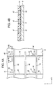
- the active matrix substrate 20 is manufactured through a first process of forming lattice-patterned wires on a substrate P, a second process of forming a stacked portion 35, and a third process of forming the pixel electrodes 45, etc.
- Figs. 3 and 4 are diagrams illustrating a wire forming process as the first process.
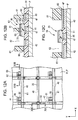
- Figs. 3B and 4B are cross-sectional views taken along Line A-A' of Figs. 3a and 4A, respectively.
- the substrate P on which the lattice-patterned wires such as the gate wires 40 and the source wires 42 are formed may be made of various materials such as glass, quartz glass, Si wafer, plastic film, metal plate, or the like.
- the substrate includes a semiconductor film, a metal film, a dielectric film, an organic film, or the like formed on the surface of the substrate made of the various materials.
- banks 51 made of insulating organic resin are formed on the substrate P.
- the banks are used to dispose wiring ink to be described later at a predetermined position of the substrate P.
- the banks 51 having a plurality of openings 52, 53, 54, 55, and 57 corresponding to positions at which the lattice-patterned wires should be formed are formed on the surface of the cleaned substrate P by using a photolithography method.
- the banks 51 may be made of a polymer material such as acryl resin, polyimide resin, olefin resin, or melamine resin.
- a lyophobic treatment is performed to the banks 51 so as to dispose the wiring ink into the openings 52, 53, 54, 55, and 57.
- a CF 4 plasma process (a plasma process with a gas containing fluorine) is carried out.
- the banks 51 may be filled with a lyophobic component (such as fluorine group) in advance.
- the openings 52, 53, 54, 55, and 57 formed by the banks 51 correspond to the lattice-patterned wires such as the gate wires 40 and the source wires 42. That is, by arranging the wiring ink in the openings 52, 53, 54, 55, and 57 of the banks 51, the lattice-patterned wires such as the gate wires 40 and the source wires 42 are formed.
- the openings 52 and 53 formed to extend in the X direction correspond to the positions at which the gate wires 40 and the capacitor lines 46 should be formed.
- the openings 54 corresponding to the positions at which the gate electrodes 41 should be formed are connected to the openings 52 corresponding to the positions at which the gate wires 40 should be formed.
- the openings 55 formed to extend in the Y direction correspond to the positions at which the source wires 42 should be formed.
- the openings 55 extending in the Y direction are divided at the intersections 56 so as not to intersect the openings 52 and 53 extending in the X direction.
- the openings 57 formed by the banks 51 correspond to the positions at which the auxiliary conductive portions 50 for electrically connecting the drain electrodes 44 to the pixel electrodes 45 should be formed.
- the lattice-patterned wires such as the gate wires 40 and the source wires 42 and the auxiliary conductive portions 50 are formed on the substrate.
- the wiring ink includes a solution in which conductive particles are dispersed in a dispersion medium or a solution in which organic silver compounds or silver oxide nanoparticles are dispersed in a solvent (dispersion medium).
- the conductive particles may include particles of conductive polymer or super-semiconductor, as well as metal particles of gold, silver, copper, tin, lead, or the like.
- the conductive particles may be coated with an organic material so as to improve the dispersion characteristic.
- the diameter of the conductive particles is in the range from 1 nm to 0.1 ⁇ m.
- the particle diameter is greater than 0.1 ⁇ m, a nozzle of a droplet ejecting head to be described later may be clogged.
- the particle diameter is smaller than 1 nm, the volume ratio of a coating agent to the conductive particles is increased and thus the ratio of organic materials contained in the resultant film is too great.
- the dispersion medium is not particularly limited if it can only disperse the conductive particles and does not cause cohesion.
- the dispersion medium may include water, alcohols such as methanol, ethanol, propanol, butanol, etc., hydrocarbon compounds such as n-heptane, n-octane, decane, dodecane, tetradecane, toluene, xylene, cymene, durene, indene, dipentene, tetrahydro naphthalene, decahydro naphthalene, cyclohexyl benzene, etc., ether compounds such as ethylene glycol dimethyl ether, ethylene glycol diethyl ether, ethylene glycol methyl ethyl ether, diethylene glycol dimethyl ether, diethylene glycol diethyl ether, diethylene glycol methyl ethyl ether, 1,2-dimethoxy ethane
- water, alcohols, hydrocarbon compounds, and ether compounds are preferable as the dispersion medium, and water and hydrocarbon compounds are most preferable as the dispersion medium.
- the surface tension of the solution in which the conductive particles are dispersed is in the range from 0.02 N/m to 0.07 N/m.
- the surface tension is smaller than 0.02 N/m, wettability of the ink compositions on the nozzle surface is increased and thus a curved ejection trajectory can be easily caused.
- the surface tension is greater than 0.07 N/m, the meniscus shape at the nozzle end is not stabilized and thus it is difficult to control the amount of ejection or the timing of ejection.
- a surface tension adjusting agent such as a fluorine agent, a silicon agent, and a nonionic agent may be slightly added to the dispersion liquid within a range in which a contact angle with the substrate is not greatly decreased.
- the nonionic surface-tension adjusting agent improves the wettability of a liquid on the substrate and the planar property of a film, thereby preventing micro unevenness of the film.
- the surface-tension adjusting agent may contain organic compounds such as alcohol, ether, ester, and ketone as needed.
- the viscosity of the dispersion liquid is in the range from 1 m ⁇ Pa ⁇ s to 50 m ⁇ Pa ⁇ s.
- the viscosity is smaller than 1 m ⁇ Pa ⁇ s, the surroundings of the nozzle can be easily contaminated due to the outflow of ink.
- the viscosity is greater than 50 m.Pa.s, the frequency of clogging of the nozzle is increased, thereby making it difficult to smoothly eject the liquid droplets.
- a dry process and a baking process are carried out as needed so as to remove the dispersion medium.
- the dry process can be performed by heating the substrate P with a hot plate, an electric furnace, or the like.
- the heating is performed, for example, at a temperature of 180°C for 60 minutes.
- the process temperature of the baking process is properly determined in consideration of the boiling point (vapor pressure) of the dispersion medium, the thermal behavior such as dispersion property or oxidation property of the particles, the amount of coating agent, the heat-proof temperature of a base material, and the like. For example, in order,to remove the coating agent made of organic materials, it is necessary to perform the baking process at a temperature of 250°C.
- the electrical contact between the conductive particles can be secured by means of the dry process and the baking process, thereby obtaining a conductive film.
- a protective metal film 47 may be formed on the wires such as the gate wires 40 or the source wires 42 and the auxiliary conductive portion 50.
- the protective metal film 47 is a thin film for suppressing a (electro) migration phenomenon of the conductive film made of silver or copper. It is preferable that the protective metal film 47 is made of nickel.
- the protective metal film 47 made of nickel is ejected and formed on the substrate P by using the liquid droplet ejecting method.
- a layer including the banks 51, the lattice-patterned wires, and the auxiliary conductive portions 50 is formed on the substrate P.
- Examples of ejection techniques of the liquid droplet ejecting method can include a charging control technique, a pressing vibration technique, an electro-mechanical conversion technique, an electro-thermal conversion technique, and an electrostatic suction technique.
- a charging control technique a material to be deposited is charged with a charging electrode and the deposition direction of the material is controlled with a deflecting electrode, thereby ejecting the material from the nozzles.
- a pressing vibration technique a high pressure of about 30 kg/cm 2 is applied to a material to eject the material from the nozzles.
- a control voltage is not applied, the material is ejected with a straight trajectory from the nozzles.
- the electro-mechanical conversion technique utilizes a property that a piezoelectric element is deformed with a pulse-like electrical signal.
- a pressure is applied to a space storing the material through a flexible material by means of the deformation of the piezoelectric element to push up the material from the space, thereby ejecting the material from the nozzles.
- the material is suddenly vaporized generating bubbles with a heater provided in the space storing the material and the material in the space is ejected by means of the pressure of the bubbles.
- the material is ejected by applying a minute pressure to the space storing the material to form a meniscus of the material at the nozzles and then applying an electrostatic attractive force.
- a technique utilizing variation in the viscosity of a fluid provided with an applied electric field or a technique of ejecting the material with discharged sparks may be used.
- the liquid droplet ejecting method has a merit that materials are negligibly wasted and a desired amount of material can be accurately deposited at a desired position.
- the amount of liquid material (fluid) to be ejected in one droplet in the liquid droplet ejecting method is about 1 to 300 ng.
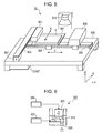
- the liquid droplet ejecting apparatus IJ shown in Fig. 5 is used as a liquid droplet ejecting apparatus used for forming the lattice-patterned wires.
- the liquid droplet ejecting apparatus (inkjet apparatus) IJ ejects (drops) droplets to the substrate P from a droplet ejecting head and includes a droplet ejecting head 301, an X direction driving axis 304, a Y direction guide axis 305, a controller CONT, a stage 307, a cleaning mechanism 308, a stand 309, and a heater 315.
- the stage 307 supports the substrate P on which ink (liquid material) is arranged by the liquid droplet ejecting apparatus IJ and includes a fixing mechanism (not shown) for fixing the substrate P to a reference position.
- the droplet ejecting head 301 is a multinozzle-type droplet ejecting head having a plurality of ejecting nozzles.
- the longitudinal direction corresponds to the Y axis direction.
- a plurality of ejecting nozzles is provided with a constant separation in the Y axis direction on the lower surface of the droplet ejecting head 301.
- the ink containing the conductive particles is ejected to the substrate P supported by the stage 307 from the ejecting nozzles of the droplet ejecting head 301.
- the X direction driving axis is connected to an X direction driving motor 302.
- the X direction driving motor 302 may be a stepping motor and rotates the X direction driving axis 304 in response to an X direction driving signal from the controller CONT.
- the X direction driving axis 304 is rotated, the droplet ejecting head 301 is moved in the X axis direction.
- the Y direction guide axis 305 is fixed to the stand 309.
- the stage 307 comprises a Y direction driving motor 303.
- the Y direction driving motor 303 may be a stepping motor and moves the stage 307 in the Y axis direction in response to a Y direction driving signal from the controller CONT.
- the controller CONT supplies a droplet ejection control voltage to the droplet ejecting head 301.
- the controller supplies a driving pulse signal for controlling the movement of the droplet ejecting head 301 in the X direction to the X direction driving motor 302 and supplies a driving pulse signal for controlling the movement of the stage 307 in the Y direction to the Y direction driving motor 303.
- the cleaning mechanism 308 cleans the droplet ejecting head 301.
- the cleaning mechanism 308 includes a Y direction driving motor (not shown).
- the cleaning mechanism 308 is moved along the Y direction guide axis 305 by means of operating the Y direction driving motor.
- the movement of the cleaning mechanism 308 is also controlled by the controller CONT.
- the heater 315 is a device for heating the substrate P by means of annealing with a lamp and performs vaporization and drying of the solvent contained in the liquid material applied on the substrate P.
- the operation of the heater 315 is also controlled by the controller CONT.
- the liquid droplet ejecting apparatus IJ ejects droplets to the substrate P while allowing the droplet ejecting head 301 to scan the stage 307 supporting the substrate P.
- the X direction is referred to as a scan direction and the Y direction perpendicular to the X direction is referred to as a nonscan direction.
- the ejecting nozzles of the droplet ejecting head 301 are arranged with a constant separation in the Y direction which is the non-scan direction.
- the droplet ejecting head 301 is disposed perpendicular to the moving direction of the substrate P, but the orientation of the droplet ejecting head 301 may be adjusted to intersect the moving direction of the substrate P.
- the orientation of the droplet ejecting head 301 it is possible to adjust the pitch between the nozzles. A distance between the substrate P and the nozzle surface may be adjusted.
- Fig. 6 is a cross-sectional view of the droplet ejecting head 301.
- the droplet ejecting head 301 is provided with a piezoelectric element 322 adjacent to a liquid chamber 321 for receiving the liquid material (wiring ink, etc.).
- the liquid chamber 321 is supplied with the liquid material through a liquid material supply system 323 including a material tank for storing the liquid material.
- the piezoelectric element 322 is connected to a driving circuit 324. By applying a voltage to the piezoelectric element 322 through the driving circuit 324 to and deforming it, the liquid chamber 321 is deformed and thus the liquid material is ejected from the nozzles 325.
- the amount of distortion of the piezoelectric element 322 is controlled by varying the value of the applied voltage.
- the speed of distortion of the piezoelectric element 322 is controlled by varying the frequency of the applied voltage. Since the ejection of droplets using the piezoelectric method does not heat the material, it does not affect the composition of the material.
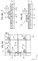
- Figs. 7 to 10 are views illustrating a process of forming a stacked portion as a second process.
- Figs. 7B to 10B are cross-sectional views taken along Line A-A' in Figs. 7A to 10A
- Figs. 8C to 10C are cross-sectional views taken along Line B-B' in Figs. 7A to 10A, respectively.
- the stacked portion 35 including an insulating film 31 and a semiconductor film (contact layer 33 and active layer 32) is formed at a predetermined position on the layer including the banks 51, the lattice-patterned wires, and the auxiliary conductive portions 50.
- the insulating film 31, the active layer 32, and the contact layer 33 are sequentially formed on the entire surface of the substrate P. Specifically, as shown in Fig. 7, a silicon nitride film as the insulating film 31, an amorphous silicon film as the active layer 32, and an n+ type silicon film as the contact layer 33 are sequentially formed by varying the raw material gas or the plasma condition.
- resists 58 are disposed at predetermined positions by using a photolithography method.
- the predetermined positions mean positions on intersections between the gate wires 40 and the source wires 42, on the gate electrodes 41, and the capacitor lines 46, as shown in Fig. 8A.
- the resist 58a disposed on the intersections 56 and the resists 58b disposed on.the capacitor lines 46 are formed so as to not contact each other.
- grooves 59 are formed in the resists 58c disposed on the gate electrodes 41 by performing a half exposure.
- the contact layer 33 and the active layer 32 are removed.
- the insulating film 31 is removed.
- the contact layer 33, the active layer 32, and the insulating film 31 are removed from the areas other than the predetermined positions at which the resists 58 (58a to 58c) are disposed.
- the stacked portion 35 including the insulating film 31 and the semiconductor film (contact layer 33 and active layer 32) is formed at the predetermined positions at which the resists 58 are disposed.
- the grooves 59 are formed in the resists 58c by performing the half exposure and thus grooves are formed by again performing the half exposure before performing the etching.
- the contact layer 33 corresponding to the grooves 59 is removed and is divided in two.
- the TFTs 30 as switching elements including the active layer 32 and the contact layer 33 are formed on the gate electrodes 41.
- a silicon nitride film as the protective film 60 for protecting the contact layer 33 is formed on the entire surface of the substrate P. In this way, the formation of the stacked portion 35 is completed.
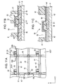
- Figs. 11 to 13 are views illustrating a process of forming the pixel electrodes 45 as a third process.
- Figs. 11B to 13B are cross-sectional views taken along Line A-A' in Figs. 11A to 13A and
- Figs. 11C to 13C are cross-sectional views taken along Line B-B' in Figs. 11A to 13A, respectively.
- the source electrodes 43, the drain electrodes 44, the connection wires 49, and the pixel electrodes 45 are formed.
- the source electrodes 43, the drain electrodes 44, the connection wires 49, and the pixel electrodes 45 may be all made of a light-transmitting material such as ITO (Indium Tin Oxide).
- the electrodes are formed using the liquid droplet ejecting method similarly to the first process.
- banks 61 are formed using the photolithography method so as to cover the gate wires 40 and the source wires 42. That is, as shown in Fig. 11, the lattice-shaped banks 61 are formed. The banks 61 cover a part of the auxiliary conductive portions 50.
- Openings 62 are formed in the intersections 56 between the source wires 42 and the gate wires 40 and between the source wires 42 and the capacitor lines 46. As shown in Fig. 11B, the openings 62 are formed to expose a part of the stacked portions 35 (TFT 30) formed on the gate electrodes 41.
- Openings 63 are formed to expose a part of the stacked portions 35 (TFT 30). Accordingly, the banks 61 are formed to divide each stacked portion 35 (TFT 30) into two parts in the X direction.
- the openings 63 are formed to expose a part of the auxiliary conductive portions 50. Accordingly, the banks 61 are formed to divide each auxiliary conductive portion 50 into two parts in the X direction.
- the banks 61 may be made of polymers such as acryl resin, polyimide resin, olefin resin, and melamine resin, similarly to the banks 51.
- the banks 61 are subjected to the lyophobic process, similarly to the banks 51.
- the openings 62 formed by the banks 61 correspond to the positions at which the connection wires 49 for connecting the divided source wires 42 or the source electrodes 43 should be formed.
- the openings 63 formed by the banks 61 correspond to the positions at which the drain electrodes 44 should be formed.
- the areas surrounded with the banks 61 correspond to the positions at which the pixel electrodes 45 should be formed.
- connection wires 49 for connecting the divided source wires 42, the source electrodes 43, the drain electrodes 44, and the pixel electrodes 45 are formed.
- a conductive material other than the transparent conductive material may be arranged in the openings 62 and 63.
- the protective film 60 formed on the entire surface of the substrate P is removed by an etching process. As a result, as shown in Fig. 12, the protective layer 60 formed in the areas in which the banks 61 are not formed is removed. The protective metal film 47 formed on the lattice-patterned wires is removed.
- the transparent conductive material is ejected and arranged in the openings 62 and 63 of the banks 61 and in the areas surrounded with the banks 61.
- a dispersion liquid in which ITO conductive particles are dispersed in a dispersion medium can be used as the transparent conductive material.
- a dry process and a baking process are performed so as to remove the dispersion medium as needed.
- the electrical contact between the conductive particles is secured, thereby obtaining a conductive film.
- connection wires 49 for connecting the divided source wires 42, the source electrodes 43, the drain electrodes 44, and the pixel electrodes 45 are formed on the substrate P.
- the method of arranging the transparent conductive material by using the liquid droplet ejecting method has been described.
- the transparent conductive material may be arranged by performing the CVD process and the etching process. In this case, the banks 61 are not required.
- the active matrix substrate 20 is manufactured through the processes described above.
- the drain electrodes 44 are formed by arranging the conductive material in the openings 63, it is possible to form the drain electrodes 44 having a sufficient thickness. That is, the contact layer 33 is lyophobic and the contact layer 33 and the pixel electrodes 45 have a height difference. Accordingly, when the openings 63 formed by the banks 61 do not exist, the conductive material flows out toward the pixel electrodes and thus the thickness of the drain electrodes 44 is reduced. Therefore, by providing the openings 63 formed by the banks 61, the conductive material can be prevented from flowing out, thereby forming the drain electrodes 44 having a sufficient thickness.
- auxiliary conductive portions 50 are formed to be exposed on the bottom surface of the openings 63, it is possible to definitely realize the electrical connection between the drain electrodes 44 and the pixel electrodes 45.
- the decrease in conductivity of the drain electrodes 45 can be prevented, thereby obtaining the active matrix substrate 20 having a desired performance.
- the case where the source wires 42 are divided at the intersections 56 has been described.
- the gate wires 40 may be divided at the intersections 56.
- the invention is not limited to the case where the wires such as the source wires 42 are divided at the intersections 56.
- the gate wires 40, the source wires 42, and the capacitor lines 46 are formed using the liquid droplet ejecting method. Accordingly, the auxiliary conductive portions 50 may be formed using the CVD method.
- liquid crystal display device 100 as an example of an electro-optical device employing the active matrix substrate 20 will be described.
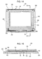
- Fig. 14 is a plan view of the liquid crystal display device 100 as shown from the counter substrate and Fig. 15 is a cross-sectional view taken along Line H-H' of Fig. 14.
- the liquid crystal display device (electro-optical device) 100 has a TFT array substrate 110 having the active matrix substrate 20 and a counter substrate 120 which are bonded to each other with a sealing member 152 as a photo-curing enclosing material.
- the liquid crystal 150 is injected and held in the area on the substrate surface.
- the sealing member 152 is formed in a closed frame shape in the substrate and has no sealing trace without a liquid crystal injection port.
- a peripheral partitioning portion 153 made of a light-shielding material is formed inside the sealing member 152.
- a data-line driving circuit 201 and mounting terminals 202 are formed along one side of the TFT array substrate 110 outside the sealing member 152 and scanning-line driving circuits 204 are formed along two sides adjacent to the one side.
- a plurality of wires 205 for connecting the scanning-line driving circuits 204 provided at both sides of the image display area are provided along the other side of the TFT array substrate 110.
- An inter-substrate electrical connection member 206 for electrically connecting the TFT array substrate 110 and the counter substrate 120 is disposed in at least one corner of the counter substrate 120.
- terminal groups formed in the peripheral portions of a TAB (Tape Automated Bonding) substrate mounted with a driving LSI and the TFT array substrate 110 may be electrically and mechanically connected through an anisotropic conductive film.
- a retardation film, a polarizing film, and the like are arranged in a predetermined direction in accordance with the kinds of the liquid crystal 150 to be used, that is, operation modes such as TN (Twisted Nematic) mode, C-TN mode, VA mode, and IPS mode, or normally-white mode/ normally-black mode, but are not shown.
- operation modes such as TN (Twisted Nematic) mode, C-TN mode, VA mode, and IPS mode, or normally-white mode/ normally-black mode, but are not shown.
- color filters of red (R), green (G), and blue (B) along with protective films thereof are formed in the areas on the counter substrate 120 opposed to the pixel electrodes on the TFT array substrate 110.
- the electro-optical device employing the active matrix substrate 20 may be an organic EL (Electroluminescence) display device.
- the organic EL display device has a structure that a thin film including inorganic and organic fluorescent compounds is interposed between a cathode and an anode.
- the organic EL display device generates excitons by injecting and exciting electrons and holes into the thin film and emits light by using the emission of light when the excitons are recombined.
- the active matrix substrate 20 having the TFTs 30 With materials exhibiting red, green, and blue colors, that is, materials for light-emitting layers, and materials for hole injecting layer and electron transport layers in an ink type and patterning the respective materials, it is possible to manufacture a self-emission full color organic EL display device.
- the active matrix substrate 20 can be applied to a surface conduction type electron emission device or the like using a phenomenon that electron emission occurs by allowing current to flow in a small-area thin film formed on PDP (Plasma Display Panel) or a substrate to be parallel to the film surface.
- PDP Plasma Display Panel
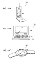
- Fig. 16A is a perspective view illustrating an example of a cellular phone.
- reference numeral 600 denotes a cellular phone body and reference numeral 601 denotes a display unit having the liquid crystal display device 100 according to the above-mentioned embodiment.
- Fig. 16B is a perspective view illustrating an example of a portable information processing apparatus such as a word processor and a personal computer.
- reference numeral 700 denotes an information processing apparatus
- reference numeral 701 denotes an input unit such as a keyboard
- reference numeral 703 denotes an information processing apparatus body
- reference numeral 702 denotes a display unit having the liquid crystal display device 100 according to the above-mentioned embodiment.
- Fig. 16C is a perspective view illustrating an example of a wristwatch-type electronic apparatus.
- reference numeral 800 denotes a watch body and reference numeral 801 denotes a display unit having the liquid crystal display device 100 according to the above-mentioned embodiment.
- the electronic apparatus may have another electro-optical device such as an organic electroluminescence display device, a plasma display device, and the like.
- the embodiment of the invention can be used in a large-sized liquid crystal panel such as a television or monitor.
Landscapes
- Physics & Mathematics (AREA)
- Nonlinear Science (AREA)
- Mathematical Physics (AREA)
- Engineering & Computer Science (AREA)
- Chemical & Material Sciences (AREA)
- Crystallography & Structural Chemistry (AREA)
- Microelectronics & Electronic Packaging (AREA)
- General Physics & Mathematics (AREA)
- Optics & Photonics (AREA)
- Liquid Crystal (AREA)
- Thin Film Transistor (AREA)
- Internal Circuitry In Semiconductor Integrated Circuit Devices (AREA)
- Devices For Indicating Variable Information By Combining Individual Elements (AREA)
- Electrodes Of Semiconductors (AREA)
Abstract
Description
- The present invention relates to an active matrix substrate, a method of manufacturing the active matrix substrate, an electro-optical device, and an electronic apparatus.
- With the spread of portable apparatuses such as notebook computers and cellular phones, thin and light liquid crystal display devices are widely used. Such liquid crystal display devices have a liquid crystal layer interposed between an upper substrate and a lower substrate.
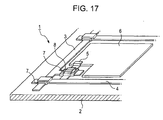
- An example of the lower substrate (an active matrix substrate) is shown in Fig. 17. As shown in the figure, the lower substrate 1 includes a
glass substrate 2,gate scanning electrodes 3 andsource electrodes 4 disposed on theglass substrate 2 to intersect each other,drain electrodes 5 disposed on theglass substrate 2, pixel electrodes (ITO) 6 connected to thedrain electrodes 5,insulating layers 7 disposed between thegate scanning electrodes 3 and thesource electrodes 4, and TFTs (thin film transistors) made of thin semiconductor material. - For example, as disclosed in Japanese Patent No. 3261699, a technique of repeatedly performing a process in which a dry process and photolithography etching are combined is used for forming metal wires in the lower substrate 1.
- A liquid droplet ejecting method is used for forming the
drain electrodes 5 and the like in the active matrix substrate described above. That is, thedrain electrodes 5 are formed by applying a conductive material between the TFTs 8 and thepixel electrodes 6 with a liquid droplet ejecting apparatus and solidifying the conductive material. - A semiconductor film constituting the TFTs 8 is subjected to a dewatering treatment and thus the semiconductor film and the
pixel electrodes 6 have a height difference (the semiconductor film is higher than the pixel electrodes 6). As a result, when the conductive material is applied between the TFTs 8 and thepixel electrodes 6, the conductive material applied onto the semiconductor film flows out toward the pixel electrodes and thus the thickness of thedrain electrodes 5 formed on the semiconductor film is reduced, thereby causing a problem that conductivity is deteriorated. - An advantage of the invention is to provide a method of manufacturing an active matrix substrate in which a conductive material can be prevented from flowing out from a semiconductor film when a conductive film is formed by applying the conductive material between a semiconductor film and pixel electrodes, thereby securing a sufficient thickness of the conductive film.
- According to a first aspect of the invention, there is provided an active matrix substrate comprising, on a substrate: lattice-patterned wires, pixel electrodes arranged in an area surrounded with the wires, and switching elements electrically connected to the wires and the pixel electrodes with a conductive film therebetween, wherein an auxiliary conductive portion electrically connecting the pixel electrodes to the conductive film is further provided.
- In the first aspect of the invention, since it is not necessary to directly form the conductive film on the pixel electrodes, it is possible to prevent the conductive material from flowing out toward the pixel electrodes.
- The auxiliary conductive portion may be formed in the same layer as the wires. Accordingly, it is possible to form the auxiliary conductive portion without increase in the number of processes.
- A bank may be provided in a part on the auxiliary conductive portion. Accordingly, since the conductive film can be located at a predetermined position, it is possible to form the conductive film having a sufficient thickness.
- According to a second aspect of the invention, there is provided a method of manufacturing an active matrix substrate comprising, on a substrate: lattice-patterned wires, pixel electrodes arranged in an area surrounded with the wires, and switching elements electrically connected to the wires and the pixel electrodes with a conductive film therebetween, wherein an auxiliary conductive portion electrically connecting the pixel electrodes to the conductive film is formed at the same time as forming the wires.
- In the second aspect of the invention, since it is not necessary to directly form the conductive film on the pixel electrodes, it is possible to prevent the conductive material from flowing out toward the pixel electrodes.
- A bank may be formed in a part on the auxiliary conductive portion before forming the conductive film by using a liquid droplet ejecting method. Accordingly, since the conductive film can be located at a predetermined position, it is possible to form the conductive film having a sufficient thickness.
- According to a third aspect of the invention, there is provided an electro-optical device comprising any one of the active matrix substrate according to the first aspect and the active matrix substrate manufactured using the method according to the second aspect. In the third aspect of the invention, it is possible to accomplish improvement of performance of the electro-optical device.
- According to a fourth aspect of the invention, there is provided an electronic apparatus comprising the electro-optical device according to the third aspect. In the fourth aspect of the invention, it is possible to accomplish improvement of performance of the electronic apparatus.
- The invention will be described with reference to the accompanying drawings, wherein like numbers reference like elements and wherein:
- Fig. 1 is a partially enlarged view of an active matrix substrate;
- Fig. 2 is an equivalent circuit diagram of the active matrix substrate;
- Fig. 3 is a diagram illustrating a procedure of manufacturing the active matrix substrate;
- Fig. 4 is a diagram illustrating a procedure subsequent to Fig. 3;
- Fig. 5 is a schematic perspective view of a liquid droplet ejecting apparatus;
- Fig. 6 is a cross-sectional view of a droplet ejecting head;
- Fig. 7 is a diagram illustrating a procedure subsequent to Fig. 4;
- Fig. 8 is a diagram illustrating a procedure subsequent to Fig. 7;
- Fig. 9 is a diagram illustrating a procedure subsequent to Fig. 8;
- Fig. 10 is a diagram illustrating a procedure subsequent to Fig. 9;
- Fig. 11 is a diagram illustrating a procedure subsequent to Fig. 10;
- Fig. 12 is a diagram illustrating a procedure subsequent to Fig. 11;
- Fig. 13 is a diagram illustrating a procedure subsequent to Fig. 12;
- Fig. 14 is a plan view of a liquid crystal display device as seen from a counter substrate;
- Fig. 15 is a cross-sectional view of the liquid crystal display device;
- Fig. 16 is a diagram illustrating a specific example of an electronic apparatus; and
- Fig. 17 is a diagram illustrating a conventional active matrix substrate.
- Hereinafter, an active matrix substrate, a method of manufacturing the active matrix substrate, an electro-optical device, and an electronic apparatus according to the present invention will be described with reference to the accompanying drawings.
- Fig. 1 is a partially enlarged view of an active matrix substrate according to the invention.
Gate wires 40 andsource wires 42 are formed in a lattice pattern on theactive matrix substrate 20. That is, a plurality ofgate wires 40 are formed to extend in the X direction and a plurality ofsource wires 42 are formed to extend in the Y direction. - The
gate wires 40 are connected togate electrodes 41 and aTFT 30 is disposed on eachgate electrode 41 with an insulating layer therebetween. On the other hand, thesource wires 42 are connected tosource electrodes 43 and one end of eachsource electrode 43 is connected to the TFT (switching element) 30. -
Pixel electrodes 45 are disposed in areas surrounded with thegate wires 40 and thesource wires 42 and each pixel electrode is connected to aTFT 30 through an auxiliaryconductive portion 50 and adrain electrode 44. - Capacitor lines.46 are formed on the
active matrix substrate 20 to be approximately parallel to thegate wires 40. Thecapacitor lines 46 are disposed under thepixel electrodes 45 and thesource wires 42 with an insulating layer therebetween. - The
gate wires 40, thegate electrodes 41, thesource wires 42, thecapacitor lines 46, and the auxiliaryconductive portion 50 are formed in the same plane. - Fig. 2 is an equivalent circuit diagram of the
active matrix substrate 20 which is used in a liquid crystal display device. - When the
active matrix substrate 20 is used in a liquidcrystal display device 100, a plurality ofpixels 100a are formed in a matrix in an image display area. In eachpixel 100a, apixel switching TFT 30 is formed and asource wire 42 for supplying pixel signals S1, S2, ..., Sn is electrically connected to the source of theTFT 30 through asource electrode 43. The pixel signals S1, S2, ..., Sn may be supplied line-sequentially to thesource wire 42 in that order and may be supplied to a plurality ofsource wires 42 adjacent to each other in a unit of groups. - The
gate wire 40 is electrically connected to the gate of theTFT 30 through agate electrode 41. At a predetermined time point, scanning signals G1, G2, ..., Gn are supplied in pulses line-sequentially to thegate wire 40 in that order. - The
pixel electrode 45 is electrically connected to the drain of theTFT 30 through adrain electrode 44. By turning on theTFT 30 as a switching element only for a predetermined period of time, the pixel signals S1, S2, ..., Sn supplied from thesource wires 42 are written to the pixels at a predetermined time point. In this way, the pixel signals with a predetermined level written to liquid crystal through thepixel electrodes 45 are held between acounter electrode 121 of acounter substrate 120 shown in Fig. 15 and the pixel electrodes for a predetermined period of time. - In order to prevent the held pixel signals S1, S2, ..., Sn from leaking,
storage capacitors 48 are provided in parallel to liquid crystal capacitors formed between thepixel electrodes 45 and thecounter electrode 121 out of the capacitor lines 46. For example, the voltage of thepixel electrodes 45 is held by thestorage capacitors 48 for a period of time that is three orders of magnitude larger than the time for which the source voltage is applied. Accordingly, the charge holding characteristic can be improved, thereby embodying the liquidcrystal display device 100 having a high contrast ratio. - Next, a method of manufacturing the
active matrix substrate 20 will be described with reference to the drawings. - The
active matrix substrate 20 is manufactured through a first process of forming lattice-patterned wires on a substrate P, a second process of forming astacked portion 35, and a third process of forming thepixel electrodes 45, etc. - Now, the respective processes are described in detail.
- Figs. 3 and 4 are diagrams illustrating a wire forming process as the first process. Figs. 3B and 4B are cross-sectional views taken along Line A-A' of Figs. 3a and 4A, respectively.
- The substrate P on which the lattice-patterned wires such as the
gate wires 40 and thesource wires 42 are formed may be made of various materials such as glass, quartz glass, Si wafer, plastic film, metal plate, or the like. The substrate includes a semiconductor film, a metal film, a dielectric film, an organic film, or the like formed on the surface of the substrate made of the various materials. - As shown in Fig. 3A, first,
banks 51 made of insulating organic resin are formed on the substrate P. The banks are used to dispose wiring ink to be described later at a predetermined position of the substrate P. - Specifically, as shown in Fig. 3, the
banks 51 having a plurality ofopenings - The
banks 51 may be made of a polymer material such as acryl resin, polyimide resin, olefin resin, or melamine resin. A lyophobic treatment is performed to thebanks 51 so as to dispose the wiring ink into theopenings banks 51 may be filled with a lyophobic component (such as fluorine group) in advance. - The
openings banks 51 correspond to the lattice-patterned wires such as thegate wires 40 and thesource wires 42. That is, by arranging the wiring ink in theopenings banks 51, the lattice-patterned wires such as thegate wires 40 and thesource wires 42 are formed. - Specifically, the
openings gate wires 40 and thecapacitor lines 46 should be formed. Theopenings 54 corresponding to the positions at which thegate electrodes 41 should be formed are connected to theopenings 52 corresponding to the positions at which thegate wires 40 should be formed. Theopenings 55 formed to extend in the Y direction correspond to the positions at which thesource wires 42 should be formed. Theopenings 55 extending in the Y direction are divided at theintersections 56 so as not to intersect theopenings - The
openings 57 formed by thebanks 51 correspond to the positions at which the auxiliaryconductive portions 50 for electrically connecting thedrain electrodes 44 to thepixel electrodes 45 should be formed. - Next, by ejecting and arranging the wiring ink containing conductive particles in the
openings gate wires 40 and thesource wires 42 and the auxiliaryconductive portions 50 are formed on the substrate. - The wiring ink includes a solution in which conductive particles are dispersed in a dispersion medium or a solution in which organic silver compounds or silver oxide nanoparticles are dispersed in a solvent (dispersion medium). The conductive particles may include particles of conductive polymer or super-semiconductor, as well as metal particles of gold, silver, copper, tin, lead, or the like. The conductive particles may be coated with an organic material so as to improve the dispersion characteristic.
- It is preferable that the diameter of the conductive particles is in the range from 1 nm to 0.1 µm. When the particle diameter is greater than 0.1 µm, a nozzle of a droplet ejecting head to be described later may be clogged. When the particle diameter is smaller than 1 nm, the volume ratio of a coating agent to the conductive particles is increased and thus the ratio of organic materials contained in the resultant film is too great.
- The dispersion medium is not particularly limited if it can only disperse the conductive particles and does not cause cohesion. Examples of the dispersion medium may include water, alcohols such as methanol, ethanol, propanol, butanol, etc., hydrocarbon compounds such as n-heptane, n-octane, decane, dodecane, tetradecane, toluene, xylene, cymene, durene, indene, dipentene, tetrahydro naphthalene, decahydro naphthalene, cyclohexyl benzene, etc., ether compounds such as ethylene glycol dimethyl ether, ethylene glycol diethyl ether, ethylene glycol methyl ethyl ether, diethylene glycol dimethyl ether, diethylene glycol diethyl ether, diethylene glycol methyl ethyl ether, 1,2-dimethoxy ethane, bis (2-methoxy ethyl) ether, p-dioxane, etc., polar compounds such as propylene carbonate, γ-butyrolactone, B-methyl-2-pyrrolidone, dimethyl formamide, dimethyl sulfoxide, cyclohexanone, etc., and so on. Among the above-mentioned compounds, from the view point of a dispersion property of particles, stability of a dispersion liquid, and easy application to the liquid droplet ejecting method (inkjet method), water, alcohols, hydrocarbon compounds, and ether compounds are preferable as the dispersion medium, and water and hydrocarbon compounds are most preferable as the dispersion medium.
- It is preferable that the surface tension of the solution in which the conductive particles are dispersed is in the range from 0.02 N/m to 0.07 N/m. In ejecting liquid by the inkjet method, when the surface tension is smaller than 0.02 N/m, wettability of the ink compositions on the nozzle surface is increased and thus a curved ejection trajectory can be easily caused. On the other hand, when the surface tension is greater than 0.07 N/m, the meniscus shape at the nozzle end is not stabilized and thus it is difficult to control the amount of ejection or the timing of ejection. In order to adjust the surface tension, a surface tension adjusting agent such as a fluorine agent, a silicon agent, and a nonionic agent may be slightly added to the dispersion liquid within a range in which a contact angle with the substrate is not greatly decreased. The nonionic surface-tension adjusting agent improves the wettability of a liquid on the substrate and the planar property of a film, thereby preventing micro unevenness of the film. The surface-tension adjusting agent may contain organic compounds such as alcohol, ether, ester, and ketone as needed.
- It is preferable that the viscosity of the dispersion liquid is in the range from 1 m·Pa·s to 50 m·Pa·s. In ejecting a liquid material in droplets by using the inkjet method, when the viscosity is smaller than 1 m·Pa·s, the surroundings of the nozzle can be easily contaminated due to the outflow of ink. When the viscosity is greater than 50 m.Pa.s, the frequency of clogging of the nozzle is increased, thereby making it difficult to smoothly eject the liquid droplets.
- After ejecting the wiring ink to the substrate P, a dry process and a baking process are carried out as needed so as to remove the dispersion medium.
- The dry process can be performed by heating the substrate P with a hot plate, an electric furnace, or the like. The heating is performed, for example, at a temperature of 180°C for 60 minutes.
- The process temperature of the baking process is properly determined in consideration of the boiling point (vapor pressure) of the dispersion medium, the thermal behavior such as dispersion property or oxidation property of the particles, the amount of coating agent, the heat-proof temperature of a base material, and the like. For example, in order,to remove the coating agent made of organic materials, it is necessary to perform the baking process at a temperature of 250°C.
- The electrical contact between the conductive particles can be secured by means of the dry process and the baking process, thereby obtaining a conductive film.
- A
protective metal film 47 may be formed on the wires such as thegate wires 40 or thesource wires 42 and the auxiliaryconductive portion 50. Theprotective metal film 47 is a thin film for suppressing a (electro) migration phenomenon of the conductive film made of silver or copper. It is preferable that theprotective metal film 47 is made of nickel. Theprotective metal film 47 made of nickel is ejected and formed on the substrate P by using the liquid droplet ejecting method. - Through the processes described above, as shown in Fig. 4, a layer including the
banks 51, the lattice-patterned wires, and the auxiliaryconductive portions 50 is formed on the substrate P. - Examples of ejection techniques of the liquid droplet ejecting method can include a charging control technique, a pressing vibration technique, an electro-mechanical conversion technique, an electro-thermal conversion technique, and an electrostatic suction technique. In the charging control technique, a material to be deposited is charged with a charging electrode and the deposition direction of the material is controlled with a deflecting electrode, thereby ejecting the material from the nozzles. In the pressing vibration technique, a high pressure of about 30 kg/cm2 is applied to a material to eject the material from the nozzles. Here, when a control voltage is not applied, the material is ejected with a straight trajectory from the nozzles. When the control voltage is applied, electrostatic repulsion occurs in the material and the material is deflected and thus not ejected from the nozzles. The electro-mechanical conversion technique utilizes a property that a piezoelectric element is deformed with a pulse-like electrical signal. Here, a pressure is applied to a space storing the material through a flexible material by means of the deformation of the piezoelectric element to push up the material from the space, thereby ejecting the material from the nozzles.
- In the electro-thermal conversion technique, the material is suddenly vaporized generating bubbles with a heater provided in the space storing the material and the material in the space is ejected by means of the pressure of the bubbles. In the electrostatic suction technique, the material is ejected by applying a minute pressure to the space storing the material to form a meniscus of the material at the nozzles and then applying an electrostatic attractive force. In addition, a technique utilizing variation in the viscosity of a fluid provided with an applied electric field or a technique of ejecting the material with discharged sparks may be used. The liquid droplet ejecting method has a merit that materials are negligibly wasted and a desired amount of material can be accurately deposited at a desired position. The amount of liquid material (fluid) to be ejected in one droplet in the liquid droplet ejecting method is about 1 to 300 ng.
- The liquid droplet ejecting apparatus IJ shown in Fig. 5 is used as a liquid droplet ejecting apparatus used for forming the lattice-patterned wires.
- The liquid droplet ejecting apparatus (inkjet apparatus) IJ ejects (drops) droplets to the substrate P from a droplet ejecting head and includes a
droplet ejecting head 301, an Xdirection driving axis 304, a Ydirection guide axis 305, a controller CONT, astage 307, acleaning mechanism 308, astand 309, and aheater 315. Thestage 307 supports the substrate P on which ink (liquid material) is arranged by the liquid droplet ejecting apparatus IJ and includes a fixing mechanism (not shown) for fixing the substrate P to a reference position. - The
droplet ejecting head 301 is a multinozzle-type droplet ejecting head having a plurality of ejecting nozzles. Here, the longitudinal direction corresponds to the Y axis direction. A plurality of ejecting nozzles is provided with a constant separation in the Y axis direction on the lower surface of thedroplet ejecting head 301. The ink containing the conductive particles is ejected to the substrate P supported by thestage 307 from the ejecting nozzles of thedroplet ejecting head 301. - The X direction driving axis is connected to an X
direction driving motor 302. The Xdirection driving motor 302 may be a stepping motor and rotates the Xdirection driving axis 304 in response to an X direction driving signal from the controller CONT. When the Xdirection driving axis 304 is rotated, thedroplet ejecting head 301 is moved in the X axis direction. - The Y
direction guide axis 305 is fixed to thestand 309. Thestage 307 comprises a Ydirection driving motor 303. The Ydirection driving motor 303 may be a stepping motor and moves thestage 307 in the Y axis direction in response to a Y direction driving signal from the controller CONT. - The controller CONT supplies a droplet ejection control voltage to the
droplet ejecting head 301. The controller supplies a driving pulse signal for controlling the movement of thedroplet ejecting head 301 in the X direction to the Xdirection driving motor 302 and supplies a driving pulse signal for controlling the movement of thestage 307 in the Y direction to the Ydirection driving motor 303. - The
cleaning mechanism 308 cleans thedroplet ejecting head 301. Thecleaning mechanism 308 includes a Y direction driving motor (not shown). Thecleaning mechanism 308 is moved along the Ydirection guide axis 305 by means of operating the Y direction driving motor. The movement of thecleaning mechanism 308 is also controlled by the controller CONT. - The
heater 315 is a device for heating the substrate P by means of annealing with a lamp and performs vaporization and drying of the solvent contained in the liquid material applied on the substrate P. The operation of theheater 315 is also controlled by the controller CONT. - The liquid droplet ejecting apparatus IJ ejects droplets to the substrate P while allowing the
droplet ejecting head 301 to scan thestage 307 supporting the substrate P. Hereinafter, the X direction is referred to as a scan direction and the Y direction perpendicular to the X direction is referred to as a nonscan direction. - Accordingly, the ejecting nozzles of the
droplet ejecting head 301 are arranged with a constant separation in the Y direction which is the non-scan direction. In Fig. 3, thedroplet ejecting head 301 is disposed perpendicular to the moving direction of the substrate P, but the orientation of thedroplet ejecting head 301 may be adjusted to intersect the moving direction of the substrate P. As a result, by adjusting the orientation of thedroplet ejecting head 301, it is possible to adjust the pitch between the nozzles. A distance between the substrate P and the nozzle surface may be adjusted. - Fig. 6 is a cross-sectional view of the
droplet ejecting head 301. - The
droplet ejecting head 301 is provided with apiezoelectric element 322 adjacent to a liquid chamber 321 for receiving the liquid material (wiring ink, etc.). The liquid chamber 321 is supplied with the liquid material through a liquidmaterial supply system 323 including a material tank for storing the liquid material. - The
piezoelectric element 322 is connected to adriving circuit 324. By applying a voltage to thepiezoelectric element 322 through the drivingcircuit 324 to and deforming it, the liquid chamber 321 is deformed and thus the liquid material is ejected from thenozzles 325. - In this case, the amount of distortion of the
piezoelectric element 322 is controlled by varying the value of the applied voltage. In addition, the speed of distortion of thepiezoelectric element 322 is controlled by varying the frequency of the applied voltage. Since the ejection of droplets using the piezoelectric method does not heat the material, it does not affect the composition of the material. - Figs. 7 to 10 are views illustrating a process of forming a stacked portion as a second process. Figs. 7B to 10B are cross-sectional views taken along Line A-A' in Figs. 7A to 10A and Figs. 8C to 10C are cross-sectional views taken along Line B-B' in Figs. 7A to 10A, respectively. In the second process, the stacked
portion 35 including an insulatingfilm 31 and a semiconductor film (contact layer 33 and active layer 32) is formed at a predetermined position on the layer including thebanks 51, the lattice-patterned wires, and the auxiliaryconductive portions 50. - First, by using a plasma CVD method, the insulating
film 31, theactive layer 32, and thecontact layer 33 are sequentially formed on the entire surface of the substrate P. Specifically, as shown in Fig. 7, a silicon nitride film as the insulatingfilm 31, an amorphous silicon film as theactive layer 32, and an n+ type silicon film as thecontact layer 33 are sequentially formed by varying the raw material gas or the plasma condition. - Next, as shown in Fig. 8, resists 58 (58a to 58c) are disposed at predetermined positions by using a photolithography method. The predetermined positions mean positions on intersections between the
gate wires 40 and thesource wires 42, on thegate electrodes 41, and thecapacitor lines 46, as shown in Fig. 8A. - The resist 58a disposed on the
intersections 56 and the resists 58b disposed on.thecapacitor lines 46 are formed so as to not contact each other. As shown in Fig. 8B,grooves 59 are formed in the resists 58c disposed on thegate electrodes 41 by performing a half exposure. - Next, by etching the entire surface of the substrate P, the
contact layer 33 and theactive layer 32 are removed. In addition, by performing an etching process, the insulatingfilm 31 is removed. - As a result, as shown in Fig. 9, the
contact layer 33, theactive layer 32, and the insulatingfilm 31 are removed from the areas other than the predetermined positions at which the resists 58 (58a to 58c) are disposed. On the other hand, the stackedportion 35 including the insulatingfilm 31 and the semiconductor film (contact layer 33 and active layer 32) is formed at the predetermined positions at which the resists 58 are disposed. - In the
stacked portions 35 formed on thegate electrodes 41, thegrooves 59 are formed in the resists 58c by performing the half exposure and thus grooves are formed by again performing the half exposure before performing the etching. As shown in Fig. 9B, thecontact layer 33 corresponding to thegrooves 59 is removed and is divided in two. As a result, theTFTs 30 as switching elements including theactive layer 32 and thecontact layer 33 are formed on thegate electrodes 41. - As shown in Fig. 10, a silicon nitride film as the
protective film 60 for protecting thecontact layer 33 is formed on the entire surface of the substrate P. In this way, the formation of the stackedportion 35 is completed. - Figs. 11 to 13 are views illustrating a process of forming the
pixel electrodes 45 as a third process. Figs. 11B to 13B are cross-sectional views taken along Line A-A' in Figs. 11A to 13A and Figs. 11C to 13C are cross-sectional views taken along Line B-B' in Figs. 11A to 13A, respectively. - In the third process, the
source electrodes 43, thedrain electrodes 44, theconnection wires 49, and thepixel electrodes 45 are formed. - The
source electrodes 43, thedrain electrodes 44, theconnection wires 49, and thepixel electrodes 45 may be all made of a light-transmitting material such as ITO (Indium Tin Oxide). The electrodes are formed using the liquid droplet ejecting method similarly to the first process. - First,
banks 61 are formed using the photolithography method so as to cover thegate wires 40 and thesource wires 42. That is, as shown in Fig. 11, the lattice-shapedbanks 61 are formed. Thebanks 61 cover a part of the auxiliaryconductive portions 50. -
Openings 62 are formed in theintersections 56 between thesource wires 42 and thegate wires 40 and between thesource wires 42 and the capacitor lines 46. As shown in Fig. 11B, theopenings 62 are formed to expose a part of the stacked portions 35 (TFT 30) formed on thegate electrodes 41. -
Openings 63 are formed to expose a part of the stacked portions 35 (TFT 30). Accordingly, thebanks 61 are formed to divide each stacked portion 35 (TFT 30) into two parts in the X direction. - The
openings 63 are formed to expose a part of the auxiliaryconductive portions 50. Accordingly, thebanks 61 are formed to divide each auxiliaryconductive portion 50 into two parts in the X direction. - In addition, the
banks 61 may be made of polymers such as acryl resin, polyimide resin, olefin resin, and melamine resin, similarly to thebanks 51. Thebanks 61 are subjected to the lyophobic process, similarly to thebanks 51. - The
openings 62 formed by thebanks 61 correspond to the positions at which theconnection wires 49 for connecting the dividedsource wires 42 or thesource electrodes 43 should be formed. Theopenings 63 formed by thebanks 61 correspond to the positions at which thedrain electrodes 44 should be formed. The areas surrounded with thebanks 61 correspond to the positions at which thepixel electrodes 45 should be formed. - That is, by arranging a transparent conductive material in the
openings banks 61 and in the areas surrounded with thebanks 61, theconnection wires 49 for connecting the dividedsource wires 42, thesource electrodes 43, thedrain electrodes 44, and thepixel electrodes 45 are formed. A conductive material other than the transparent conductive material may be arranged in theopenings - Next, the
protective film 60 formed on the entire surface of the substrate P is removed by an etching process. As a result, as shown in Fig. 12, theprotective layer 60 formed in the areas in which thebanks 61 are not formed is removed. Theprotective metal film 47 formed on the lattice-patterned wires is removed. - Next, the transparent conductive material is ejected and arranged in the
openings banks 61 and in the areas surrounded with thebanks 61. A dispersion liquid in which ITO conductive particles are dispersed in a dispersion medium can be used as the transparent conductive material. - After ejecting the transparent conductive material to the substrate P, a dry process and a baking process are performed so as to remove the dispersion medium as needed. By means of the dry process and the baking process, the electrical contact between the conductive particles is secured, thereby obtaining a conductive film.
- As a result, as shown in Fig. 13, the
connection wires 49 for connecting the dividedsource wires 42, thesource electrodes 43, thedrain electrodes 44, and thepixel electrodes 45 are formed on the substrate P. - In the embodiments, the method of arranging the transparent conductive material by using the liquid droplet ejecting method has been described. However, the transparent conductive material may be arranged by performing the CVD process and the etching process. In this case, the
banks 61 are not required. - The
active matrix substrate 20 is manufactured through the processes described above. - Since the
drain electrodes 44 are formed by arranging the conductive material in theopenings 63, it is possible to form thedrain electrodes 44 having a sufficient thickness. That is, thecontact layer 33 is lyophobic and thecontact layer 33 and thepixel electrodes 45 have a height difference. Accordingly, when theopenings 63 formed by thebanks 61 do not exist, the conductive material flows out toward the pixel electrodes and thus the thickness of thedrain electrodes 44 is reduced. Therefore, by providing theopenings 63 formed by thebanks 61, the conductive material can be prevented from flowing out, thereby forming thedrain electrodes 44 having a sufficient thickness. - Since the auxiliary
conductive portions 50 are formed to be exposed on the bottom surface of theopenings 63, it is possible to definitely realize the electrical connection between thedrain electrodes 44 and thepixel electrodes 45. - As a result, the decrease in conductivity of the
drain electrodes 45 can be prevented, thereby obtaining theactive matrix substrate 20 having a desired performance. - In the embodiment, the case where the
source wires 42 are divided at theintersections 56 has been described. However, thegate wires 40 may be divided at theintersections 56. - The invention is not limited to the case where the wires such as the
source wires 42 are divided at theintersections 56. - Although the case where the
gate wires 40, thesource wires 42, and thecapacitor lines 46 are formed using the liquid droplet ejecting method has been described, they may be formed using a CVD method. Accordingly, the auxiliaryconductive portions 50 may be formed using the CVD method. - Next, a liquid
crystal display device 100 as an example of an electro-optical device employing theactive matrix substrate 20 will be described. - Fig. 14 is a plan view of the liquid
crystal display device 100 as shown from the counter substrate and Fig. 15 is a cross-sectional view taken along Line H-H' of Fig. 14. - In the drawings referred to in the following description, in order to recognize the layers and the members, scales of the layers and the members are different.
- In Figs. 14 and 15, the liquid crystal display device (electro-optical device) 100 has a
TFT array substrate 110 having theactive matrix substrate 20 and acounter substrate 120 which are bonded to each other with a sealingmember 152 as a photo-curing enclosing material. Theliquid crystal 150 is injected and held in the area on the substrate surface. The sealingmember 152 is formed in a closed frame shape in the substrate and has no sealing trace without a liquid crystal injection port. - A
peripheral partitioning portion 153 made of a light-shielding material is formed inside the sealingmember 152. A data-line driving circuit 201 and mountingterminals 202 are formed along one side of theTFT array substrate 110 outside the sealingmember 152 and scanning-line driving circuits 204 are formed along two sides adjacent to the one side. A plurality ofwires 205 for connecting the scanning-line driving circuits 204 provided at both sides of the image display area are provided along the other side of theTFT array substrate 110. An inter-substrateelectrical connection member 206 for electrically connecting theTFT array substrate 110 and thecounter substrate 120 is disposed in at least one corner of thecounter substrate 120. - Instead of forming the data-
line driving circuit 201 and the scanning-line driving circuits 204 on theTFT array substrate 110, terminal groups formed in the peripheral portions of a TAB (Tape Automated Bonding) substrate mounted with a driving LSI and theTFT array substrate 110 may be electrically and mechanically connected through an anisotropic conductive film. - In the liquid
crystal display device 100, a retardation film, a polarizing film, and the like are arranged in a predetermined direction in accordance with the kinds of theliquid crystal 150 to be used, that is, operation modes such as TN (Twisted Nematic) mode, C-TN mode, VA mode, and IPS mode, or normally-white mode/ normally-black mode, but are not shown. - When the liquid
crystal display device 100 is formed for color display, color filters of red (R), green (G), and blue (B) along with protective films thereof are formed in the areas on thecounter substrate 120 opposed to the pixel electrodes on theTFT array substrate 110. - The electro-optical device employing the
active matrix substrate 20 may be an organic EL (Electroluminescence) display device. - The organic EL display device has a structure that a thin film including inorganic and organic fluorescent compounds is interposed between a cathode and an anode. The organic EL display device generates excitons by injecting and exciting electrons and holes into the thin film and emits light by using the emission of light when the excitons are recombined.
- By providing the
active matrix substrate 20 having theTFTs 30 with materials exhibiting red, green, and blue colors, that is, materials for light-emitting layers, and materials for hole injecting layer and electron transport layers in an ink type and patterning the respective materials, it is possible to manufacture a self-emission full color organic EL display device. - The
active matrix substrate 20 can be applied to a surface conduction type electron emission device or the like using a phenomenon that electron emission occurs by allowing current to flow in a small-area thin film formed on PDP (Plasma Display Panel) or a substrate to be parallel to the film surface. - Next, a specific example of an electronic apparatus according to the invention will be described.
- Fig. 16A is a perspective view illustrating an example of a cellular phone. In Fig. 16A,
reference numeral 600 denotes a cellular phone body andreference numeral 601 denotes a display unit having the liquidcrystal display device 100 according to the above-mentioned embodiment. - Fig. 16B is a perspective view illustrating an example of a portable information processing apparatus such as a word processor and a personal computer. In Fig. 16B,
reference numeral 700 denotes an information processing apparatus,reference numeral 701 denotes an input unit such as a keyboard,reference numeral 703 denotes an information processing apparatus body, andreference numeral 702 denotes a display unit having the liquidcrystal display device 100 according to the above-mentioned embodiment. - Fig. 16C is a perspective view illustrating an example of a wristwatch-type electronic apparatus. In Fig. 16C,
reference numeral 800 denotes a watch body andreference numeral 801 denotes a display unit having the liquidcrystal display device 100 according to the above-mentioned embodiment. - As a result, since the electronic apparatuses shown in Figs. 16A to 16C have the liquid
crystal display device 100 according to the above-mentioned embodiment, it is possible to obtain high quality and performance. - Although the electronic apparatus according to the embodiment has the liquid
crystal display device 100, the electronic apparatus may have another electro-optical device such as an organic electroluminescence display device, a plasma display device, and the like. - The embodiment of the invention can be used in a large-sized liquid crystal panel such as a television or monitor.
- Although the exemplary embodiments of the present invention have been hitherto described with reference to the accompanying drawings, the invention is not limited to the exemplary embodiments. The shapes or combinations of the elements shown in the exemplary embodiments are only examples and can be variously changed in response to design requirements without departing from the gist of the invention.
Claims (7)
- An active matrix substrate comprising, on a substrate:lattice-patterned wires, pixel electrodes arranged in an area surrounded with the wires, and switching elements electrically connected to the wires and the pixel electrodes with a conductive film therebetween,wherein an auxiliary conductive portion electrically connecting the pixel electrodes to the conductive film is further provided.
- The active matrix substrate according to Claim 1, wherein the auxiliary conductive portion is formed in the same layer as the wires.
- The active matrix substrate according to Claim 1, wherein a bank is provided in a part of the auxiliary conductive portion.
- A method of manufacturing an active matrix substrate comprising, on a substrate: lattice-patterned wires, pixel electrodes arranged in an area surrounded with the wires, and switching elements electrically connected to the wires and the pixel electrodes with a conductive film therebetween,
wherein an auxiliary conductive portion electrically connecting the pixel electrodes to the conductive film is formed at the same time as forming the wires. - The method according to Claim 4, wherein a bank is formed in a part of the auxiliary conductive portion before forming the conductive film by using a liquid droplet ejecting method.
- An electro-optical device comprising one of the active matrix substrate according to Claim 1 and the active matrix substrate manufactured using the method according to Claim 4.
- An electronic apparatus comprising the electro-optical device according to Claim 6.
Applications Claiming Priority (1)
| Application Number | Priority Date | Filing Date | Title |
|---|---|---|---|
| JP2004247919A JP2006065020A (en) | 2004-08-27 | 2004-08-27 | Active matrix substrate manufacturing method, active matrix substrate, electro-optical device, and electronic apparatus |
Publications (2)
| Publication Number | Publication Date |
|---|---|
| EP1630869A2 true EP1630869A2 (en) | 2006-03-01 |
| EP1630869A3 EP1630869A3 (en) | 2015-02-11 |
Family
ID=35414667
Family Applications (1)
| Application Number | Title | Priority Date | Filing Date |
|---|---|---|---|
| EP05018371.4A Withdrawn EP1630869A3 (en) | 2004-08-27 | 2005-08-24 | Active matrix substrate, method of manufacturing active matrix substrate, electro-optical device, and electronic apparatus |
Country Status (6)
| Country | Link |
|---|---|
| US (1) | US7477336B2 (en) |
| EP (1) | EP1630869A3 (en) |
| JP (1) | JP2006065020A (en) |
| KR (1) | KR100716217B1 (en) |
| CN (1) | CN100399566C (en) |
| TW (1) | TWI283789B (en) |
Cited By (2)
| Publication number | Priority date | Publication date | Assignee | Title |
|---|---|---|---|---|
| EP1701206A1 (en) * | 2005-03-09 | 2006-09-13 | Seiko Epson Corporation | Pixel structure, active matrix substrate, method of manufacturing active matrix substrate, electro-optical device, and electronic apparatus |
| US10937897B2 (en) | 2008-07-31 | 2021-03-02 | Semiconductor Energy Laboratory Co., Ltd. | Semiconductor device and method for manufacturing the same |
Families Citing this family (5)
| Publication number | Priority date | Publication date | Assignee | Title |
|---|---|---|---|---|
| JP4572814B2 (en) * | 2005-11-16 | 2010-11-04 | セイコーエプソン株式会社 | Active matrix substrate, manufacturing method thereof, electro-optical device, and electronic apparatus |
| KR101340727B1 (en) * | 2006-09-11 | 2013-12-12 | 엘지디스플레이 주식회사 | Method for Fabricating Thin Film Pattern, Liquid Crystal Display Panel and Method for Fabricating Thereof Using the same |
| TWI356249B (en) * | 2007-10-26 | 2012-01-11 | Au Optronics Corp | Liquid crystal display panel and liquid crystal di |
| CN101814511B (en) * | 2009-02-23 | 2012-11-21 | 北京京东方光电科技有限公司 | TFT-LCD (Thin Film Transistor Liquid Crystal Display) array substrate and manufacture method thereof |
| KR102774286B1 (en) * | 2019-12-05 | 2025-02-26 | 엘지디스플레이 주식회사 | Thin film transistor array substrate for digital x-ray detector, the digital x-ray detector and manufacturing method thereof |
Family Cites Families (15)
| Publication number | Priority date | Publication date | Assignee | Title |
|---|---|---|---|---|
| JPH02170135A (en) | 1988-12-23 | 1990-06-29 | Nec Corp | Thin-film field effect type transistor element array |
| JPH06160904A (en) | 1992-11-26 | 1994-06-07 | Matsushita Electric Ind Co Ltd | Liquid crystal display device and manufacturing method thereof |
| JP2898509B2 (en) * | 1993-06-23 | 1999-06-02 | シャープ株式会社 | Active matrix substrate and manufacturing method thereof |
| CN101369579B (en) * | 1995-10-03 | 2011-05-04 | 精工爱普生株式会社 | Method for manufacturing active matrix substrate and film element |
| JP3367821B2 (en) * | 1996-06-03 | 2003-01-20 | シャープ株式会社 | Active matrix substrate |
| JPH1020336A (en) * | 1996-07-02 | 1998-01-23 | Sharp Corp | Active matrix substrate and manufacturing method thereof |
| JP3622934B2 (en) * | 1996-07-31 | 2005-02-23 | エルジー フィリップス エルシーディー カンパニー リミテッド | Thin film transistor type liquid crystal display device |
| JP3916823B2 (en) * | 1999-04-07 | 2007-05-23 | シャープ株式会社 | Active matrix substrate, manufacturing method thereof, and flat panel image sensor |
| US6380559B1 (en) | 1999-06-03 | 2002-04-30 | Samsung Electronics Co., Ltd. | Thin film transistor array substrate for a liquid crystal display |
| KR20010046141A (en) * | 1999-11-10 | 2001-06-05 | 구본준 | Method for forming a signal line and TFT using the method |
| JP3597769B2 (en) | 2000-09-18 | 2004-12-08 | シャープ株式会社 | Manufacturing method of electronic components |
| JP4042099B2 (en) * | 2002-04-22 | 2008-02-06 | セイコーエプソン株式会社 | Device manufacturing method, device and electronic apparatus |
| JP3965562B2 (en) | 2002-04-22 | 2007-08-29 | セイコーエプソン株式会社 | Device manufacturing method, device, electro-optical device, and electronic apparatus |
| JP3787839B2 (en) * | 2002-04-22 | 2006-06-21 | セイコーエプソン株式会社 | Device manufacturing method, device and electronic apparatus |
| JP2004062152A (en) * | 2002-06-03 | 2004-02-26 | Sharp Corp | Display device using bidirectional two-terminal element and method of manufacturing the same |
-
2004
- 2004-08-27 JP JP2004247919A patent/JP2006065020A/en active Pending
-
2005
- 2005-07-26 KR KR1020050067657A patent/KR100716217B1/en not_active Expired - Lifetime
- 2005-08-01 TW TW094126066A patent/TWI283789B/en not_active IP Right Cessation
- 2005-08-19 CN CNB2005100926330A patent/CN100399566C/en not_active Expired - Lifetime
- 2005-08-24 EP EP05018371.4A patent/EP1630869A3/en not_active Withdrawn
- 2005-08-26 US US11/212,401 patent/US7477336B2/en active Active
Cited By (4)
| Publication number | Priority date | Publication date | Assignee | Title |
|---|---|---|---|---|
| EP1701206A1 (en) * | 2005-03-09 | 2006-09-13 | Seiko Epson Corporation | Pixel structure, active matrix substrate, method of manufacturing active matrix substrate, electro-optical device, and electronic apparatus |
| US7567309B2 (en) | 2005-03-09 | 2009-07-28 | Seiko Epson Corporation | Pixel electrodes and switching elements formed on same substrate in openings of insulating film formed on the substrate |
| US10937897B2 (en) | 2008-07-31 | 2021-03-02 | Semiconductor Energy Laboratory Co., Ltd. | Semiconductor device and method for manufacturing the same |
| US12074210B2 (en) | 2008-07-31 | 2024-08-27 | Semiconductor Energy Laboratory Co., Ltd. | Semiconductor device and method for manufacturing the same |
Also Published As
| Publication number | Publication date |
|---|---|
| KR100716217B1 (en) | 2007-05-10 |
| CN100399566C (en) | 2008-07-02 |
| CN1741272A (en) | 2006-03-01 |
| TW200609634A (en) | 2006-03-16 |
| JP2006065020A (en) | 2006-03-09 |
| KR20060046763A (en) | 2006-05-17 |
| EP1630869A3 (en) | 2015-02-11 |
| US7477336B2 (en) | 2009-01-13 |
| US20060044486A1 (en) | 2006-03-02 |
| TWI283789B (en) | 2007-07-11 |
Similar Documents
| Publication | Publication Date | Title |
|---|---|---|
| US7767504B2 (en) | Methods for forming film patterns by disposing a liquid within a plural-level partition structure | |
| EP1643300A1 (en) | Barrier structure for forming a conductive pattern by ink jet printing | |
| US7477336B2 (en) | Active matrix substrate, method of manufacturing active matrix substrate, electro-optical device, and electronic apparatus | |
| US7517735B2 (en) | Method of manufacturing active matrix substrate, active matrix substrate, electro-optical device, and electronic apparatus | |
| US7524764B2 (en) | Method of forming film pattern, device, method of manufacturing the same, electro-optical apparatus, and electronic apparatus | |
| JP4380552B2 (en) | Active matrix substrate manufacturing method, active matrix substrate, electro-optical device, and electronic apparatus | |
| KR100841284B1 (en) | Metal wiring formation method and active matrix substrate manufacturing method | |
| US7691562B2 (en) | Method for forming film pattern, and method for manufacturing device, electro-optical device, electronic apparatus and active matrix substrate | |
| EP1648210B1 (en) | Bank structure for defining wire-formation regions | |
| US7560297B2 (en) | Active matrix substrate, manufacturing method thereof, electro-optical device, and electronic apparatus | |
| JP2006019630A (en) | Wiring formation method | |
| JP2004311530A (en) | Pattern forming method, device and manufacturing method thereof, liquid crystal display device manufacturing method, plasma display panel manufacturing method, organic EL device manufacturing method, field emission display manufacturing method, electro-optical device, and electronic equipment | |
| JP2004330164A (en) | Thin-film pattern forming method, device and manufacturing method thereof, electro-optical device, and electronic apparatus | |
| JP2006065019A (en) | Active matrix substrate manufacturing method, active matrix substrate, electro-optical device, and electronic apparatus | |
| JP2007139953A (en) | Active matrix substrate, manufacturing method thereof, electro-optical device, and electronic apparatus | |
| CN100579336C (en) | Method for forming metal wiring and method for manufacturing active matrix substrate | |
| JP2007189130A (en) | Device, manufacturing method thereof, wiring forming method, electro-optical device, and electronic apparatus | |
| JP2007142023A (en) | Device, manufacturing method thereof, wiring forming method, electro-optical device, and electronic apparatus | |
| JP2006332313A (en) | Conductive film pattern forming method, device manufacturing method, electro-optical device, and electronic apparatus | |
| JP2008058455A (en) | Method for manufacturing active matrix substrate and method for manufacturing liquid crystal display device | |
| JP2008058456A (en) | Method for manufacturing active matrix substrate and method for manufacturing liquid crystal display device |
Legal Events
| Date | Code | Title | Description |
|---|---|---|---|
| PUAI | Public reference made under article 153(3) epc to a published international application that has entered the european phase |
Free format text: ORIGINAL CODE: 0009012 |
|
| AK | Designated contracting states |
Kind code of ref document: A2 Designated state(s): AT BE BG CH CY CZ DE DK EE ES FI FR GB GR HU IE IS IT LI LT LU LV MC NL PL PT RO SE SI SK TR |
|
| AX | Request for extension of the european patent |
Extension state: AL BA HR MK YU |
|
| PUAL | Search report despatched |
Free format text: ORIGINAL CODE: 0009013 |
|
| AK | Designated contracting states |
Kind code of ref document: A3 Designated state(s): AT BE BG CH CY CZ DE DK EE ES FI FR GB GR HU IE IS IT LI LT LU LV MC NL PL PT RO SE SI SK TR |
|
| AX | Request for extension of the european patent |
Extension state: AL BA HR MK YU |
|
| RIC1 | Information provided on ipc code assigned before grant |
Ipc: H01L 27/12 20060101AFI20150108BHEP |
|
| AKY | No designation fees paid | ||
| AXX | Extension fees paid |
Extension state: HR Extension state: AL Extension state: YU Extension state: BA Extension state: MK |
|
| REG | Reference to a national code |
Ref country code: DE Ref legal event code: R108 |
|
| STAA | Information on the status of an ep patent application or granted ep patent |
Free format text: STATUS: THE APPLICATION IS DEEMED TO BE WITHDRAWN |
|
| 18D | Application deemed to be withdrawn |
Effective date: 20150812 |