EP1629266B1 - Optical substrate for enhanced detectability of fluorescence - Google Patents
Optical substrate for enhanced detectability of fluorescence Download PDFInfo
- Publication number
- EP1629266B1 EP1629266B1 EP04735866.8A EP04735866A EP1629266B1 EP 1629266 B1 EP1629266 B1 EP 1629266B1 EP 04735866 A EP04735866 A EP 04735866A EP 1629266 B1 EP1629266 B1 EP 1629266B1
- Authority
- EP
- European Patent Office
- Prior art keywords
- layers
- substrate
- wavelength
- layer
- sample
- Prior art date
- Legal status (The legal status is an assumption and is not a legal conclusion. Google has not performed a legal analysis and makes no representation as to the accuracy of the status listed.)
- Expired - Lifetime
Links
Images


Classifications
-
- G—PHYSICS
- G02—OPTICS
- G02B—OPTICAL ELEMENTS, SYSTEMS OR APPARATUS
- G02B5/00—Optical elements other than lenses
- G02B5/20—Filters
- G02B5/28—Interference filters
- G02B5/285—Interference filters comprising deposited thin solid films
-
- G—PHYSICS
- G01—MEASURING; TESTING
- G01N—INVESTIGATING OR ANALYSING MATERIALS BY DETERMINING THEIR CHEMICAL OR PHYSICAL PROPERTIES
- G01N21/00—Investigating or analysing materials by the use of optical means, i.e. using sub-millimetre waves, infrared, visible or ultraviolet light
- G01N21/62—Systems in which the material investigated is excited whereby it emits light or causes a change in wavelength of the incident light
- G01N21/63—Systems in which the material investigated is excited whereby it emits light or causes a change in wavelength of the incident light optically excited
- G01N21/64—Fluorescence; Phosphorescence
- G01N21/645—Specially adapted constructive features of fluorimeters
- G01N21/6452—Individual samples arranged in a regular 2D-array, e.g. multiwell plates
-
- G—PHYSICS
- G01—MEASURING; TESTING
- G01N—INVESTIGATING OR ANALYSING MATERIALS BY DETERMINING THEIR CHEMICAL OR PHYSICAL PROPERTIES
- G01N21/00—Investigating or analysing materials by the use of optical means, i.e. using sub-millimetre waves, infrared, visible or ultraviolet light
- G01N21/01—Arrangements or apparatus for facilitating the optical investigation
- G01N21/03—Cuvette constructions
- G01N21/0303—Optical path conditioning in cuvettes, e.g. windows; adapted optical elements or systems; path modifying or adjustment
Definitions
- the present invention relates to a sample substrate adapted for use with fluorescence excitation light.
- substrates as plates, slides and cells, are used e.g. in examining, indicating, analyzing or identifying fluorescent, phosphorescent or luminescent sample materials, e.g. tagged molecular biological specimens.
- Fluorescence microscopy is often used in the fields of molecular biology, biochemistry and other life sciences for analyzing biological molecules, including nucleic acids (DNA, RNA) and proteins (enzymes, antigens, etc.) that have been tagged or labeled with fluorescent probes.
- DNA diagnostics such as for gene detection, in which a DNA sample is deposited on and bound to a glass substrate. The bound DNA on the substrate can then be imaged by fluorescence. The fluorescence of a sample was originally assessed by visual inspection through a conventional microscope, but this manual method has proved time-consuming and costly. Many different high-speed automated fluorescence imaging systems are now available.
- SNR signal-to-noise ratio
- PMT photomultiplier tube
- Sources of background noise include specular or diffuse reflection of the fluorescence-stimulating laser light from the sample, autofluorescence of the substrate holding the sample, autofluorescence from the optics in the light path of the optical imaging system, stray light, and dark current of the detector. Stray light reaching the detector can be significantly reduced by proper size and placement of apertures in the imaging system. Both stray light and much of the reflected laser light can be rejected, while passing the fluorescent light, by using dichroic and other spectral filters and beamsplitters in the system. Autofluorescence of the optical elements can be reduced by avoiding use of lens cements in the light path, using glass instead of polymeric lenses, or using curved mirrors instead of lenses wherever possible.
- Autofluorescence of the substrate can be reduced by using low fluorescence materials, such as an ultrathin or opaque glass substrate.
- low fluorescence materials such as an ultrathin or opaque glass substrate.
- Strongin discloses a plastic slide that is rendered opaque and substantially nonfluorescent with a quantity of black carbon powder in the plastic.
- Another way of handling autofluorescence is to use a pulsed or modulated excitation and to take advantage of the differences in emission decay rates between background fluorescence and specimen fluorescence, as disclosed in U.S. Pat. Nos. 4,877,965 to Dandliker et al . and 5,091,653 to Creager et al .
- Bogart discloses an assay system and method for detecting the presence or amount of an analyte of interest. It includes a test substrate with an optically active surface that enhances the color contrast, i.e. differences in the observed wavelength (or combination of wavelengths) of light from the surface, between the presence and absence of the analyte in a sample applied onto the test substrate.
- the substrate may comprise a reflective solid optical base, such as a silicon wafer or metallic (e.g., aluminum) base, with an optical thin film coating thereon.
- the coating may comprise several layers, including for example an attachment layer on the upper surface of the base, and a receptive layer on the upper surface of the attachment layer containing a specific binding partner for the analyte of interest.
- the total coating thickness is selected to cause incident light to undergo thin film interference upon reflection, such that a specific color is produced.
- the coating material(s) should have an overall thickness of a quarterwave of the unwanted color to be attenuated so that destructive interference of that color will occur.
- the substrate therefore has a particular background color, which can then be used as a comparative reference against a different observed color when an analyte of interest is present. Both qualitative visual inspection and quantitative instrumented measurement are suggested. Polarization contrast by means of an ellipsometer is also suggested.
- OIA optical immunoassay
- Commercial products include test kits for group A and group B streptococci and for chlamydia trachomatis.
- Bogart further discloses, in another embodiment of his approach (FIG. 17 of the aforementioned patent), the use of these substrates for enhanced fluorescence detection.
- fluorescent label molecules may be attached to the analyte.
- the fluorescent molecules may be attached to any suitably selective and specific receptive material or reagent, such as a secondary antibody, and applied to the surface.
- the fluorescent labels are thus bound to the analyte of interest on the surface, if present, and immobilized to the surface through the analyte bridge.
- Directing light of an excitation wavelength onto the surface stimulates fluorescence of any of the label bound to the surface, thereby revealing the presence of the analyte of interest.
- the reflective substrate may have an antireflection layer whose thickness is selected to suppress reflection of the excitation wavelength, thereby reducing the background noise reaching the detector.
- Bogart states that the fluorescent signal generation is not dependent on the film thickness. Though the fluorescence signal S might be increased by increasing the output power of the laser, reflected laser noise will also increase, with possibly little improvement in the resulting SNR.
- a sample substrate which is reflective for the excitation wavelength.
- This substrate has a transparent coating layer thereon with controlled thickness that has been selected to ensure that a molecular sample placed on top of the coating layer is located at an antinode for the excitation light.
- the substrate includes a rigid base with a specularly reflective upper surface.
- the transparent coating on the upper surface of the base has a thickness selected such that for a particular excitation wavelength of light at normal incidence, the optical path from the top of the coating to the base reflecting surface is substantially an odd multiple (1, 3, 5, etc.) of one-quarter wavelength of the excitation light.
- the optical path length of the material is defined by the wavelength of light, the index of refraction of the material, and the angle of propagation through the material.
- the reflecting surface of the base is at a well defined depth slightly below the physical surface of the base by an amount equal to the sum of the skin (or penetration) depth of the reflective surface material and the optical depth of any surface oxidation on the base.
- the base can be made completely of metal or may be composed of a rigid bottom layer with a top metal coating.
- the metal can be aluminum, silver, gold or rhodium.
- the transparent coating may be a single layer of dielectric material, such as silica, alumina or a fluoride material (such as MgF 2 ).
- the transparent coating could be a multilayer coating with the top layer being a chemically reactive material for .binding a specified biological sample constituent thereto.
- Kains concept of applying a transparent quarterwave layer on a reflecting surface is limited to reflectors with rigid surfaces. Here light is not penetrating beneath the physical surface of the reflector or the penetration is limited to at most some nanometers beneath the surface (skin depth). Practically this represents a limitation to metallic surfaces such as metal substrates or metallic coatings.
- Chaton et al give one example in WO 02/48691 where this effect can be seen. Chaton et al describe the use of dielectric quarterwave stacks which have a mirror function on a silicon substrate in order to enhance the fluorescence.
- the reflectivity of silicium at 550nm is at about 42%. This results in a square electromagnetic field amplitude (E 2 ) on the metallic surface of about 10% of the square of the field amplitude of the free propagating wave E 2 (PW).
- Chaton et al use a quarterwave stack with a design wavelength of 550nm in order to reinforce reflectivity. This means that a system of alternating high and low index dielectric layers is used to increase. the reflectivity, where each individual layer has an optical thickness of one quarter of the design wavelength.
- Chaton et al use a five layer system on silicon with SiO 2 (94nm layer thickness, 3 layers) and Si 3 N 4 (69nm layer thickness, 2 layers) as coating materials.
- Mirrors based on quarterwave stacks are known as Bragg mirrors. Typically such a Bragg mirror is based on a quarterwave stack where the outermost layer is a high index layer.
- Chaton et al use as outermost quarterwave layer an SiO 2 layer, which is the low index material. It is known that the outermost layer being a low index layer results in lower reflection values. Removing the outermost layer (low index layer) would even result in higher reflectivity.
- the Chaton et al describe they use SiO 2 as outermost layer in order to create a physical surface which is compatible with the linker chemistry.
- WO 02/48691 Al discloses fluorescence enhancement by depositing a stack of quarter-wave type layers.
- the reflection band is centered at the design wavelength of 550nm and is 200nm broad. Within the reflection band the reflectivity is increased to slightly below 60%. Because Chaton et al did not take into account the antinode condition, they conclude that the quarterwave stack is effectively enhancing the fluorescence signal for wavelengths between 450nm to 650nm. This wavelength range comprises the wavelengths of the fluorescence materials typically used for fluorescence lables such as CY3 and CY5. Unfortunately only for the design wavelength the antinode condition is well fulfilled. For an excitation wavelength much different from 550nm this condition is not fulfilled. For 450nm the enhancement factor is as low as 0.2 and for 650nm the enhancement factor decreases down to 1.2.
- the sample substrate according to the present invention has an optical structure which is adapted for enhancing fluorescence detection and imaging.
- the format of the sample substrate according to the present invention can be adapted to formats which are typically used in the addressed field, such as e.g. the standard format of microtiter plates.
- a sample substrate which has not anymore the disadvantage to base the reflection of the excitation wavelength completely on the reflectivity of a metal surface.
- a sample substrate may be realized which provides a maximum enhancement of the fluorescence signal for two or more than two different excitation wavelengths.
- application-adjusted enhancement factors for two or more excitation wavelengths are provided, whereby such sample substrates as of the present invention are preferably manufactured by the method as was addressed above with its different embodiments.
- One embodiment of the reflective sample substrate according to the present invention has an interference reflector based on a dielectric multilayer coating.
- the excitation light is reflected with 100% or close to 100%.
- the resulting electromagnetic field distribution connected to the excitation wavelength outside the sample substrate in the cover region is therefore a standing wave or close to a standing wave with planes of nodes and planes of antinodes.
- the layers of the interference reflector may have an optimized thickness distribution that has been selected to ensure that an areal fluorescent sample placed on top of the top coating layer is located in the plane of an antinode of the excitation light.
- the electrical field distribution within such an interference reflector is very different from the field distribution known from specular reflection of a metal surface.
- An additional layer added on top of the interference reflector can cause a decrease in reflectance.
- the inventors investigated the electromagnetic field distribution within the substrate samples they had optimized with the help of such an optimization procedure. They investigated the sample substrates providing enhanced maximum electromagnetic field intensity at the physical surface of the sample for various designs including prior art solutions as disclosed by Kain et al as well as Chaton et al. They found that the electromagnetic field distribution provides a minimum which is located one quarterwave below the physical surface. This was independent how deep actually the electromagnetic field propagates into the samples. In accordance with the invention, the electromagnetic field needs to provide a minimum which is located approximately one quarterwave beneath the physical surface.
- the sample substrate of the present invention can be used in any of a wide number of possible fluorescence microscope systems, including, for example, those described in U.S. Pat. Nos. 4,284,897 to Sawamura et al ., 5,091,652 to Mathies et al ., 5,296,700 to Kumagai , 5,381,224 to Dixon et al ., and 5,504,336 to Noguchi , as well as U.S. patent application Ser. Nos. 08/595,355 , 08/616,174 and 08/791,684 .
- a preferred fluorescence imaging system 1 for use with the present invention is illustrated in FIG. 1 :
- the stimulating beam 11 is preferably a collimated beam of monochromatic coherent light.
- a noncoherent source such as a light emitting diode (LED) could be used and a noncollimated source could be coupled to collimating optics to create a collimated beam. If the stimulating beam 11 is not monochromatic, it may be directed through a filter to reduce any unwanted wavelengths.
- the stimulating beam 11 is then directed through lens systems 12, 12' and a beam splitter 15 onto the surface of the sample substrate 20.
- Any scanning mechanism that produces a two-dimensional scan may be used to move the substrate along orthogonal axis in plane with the surface of the sample substrate.
- the lens system 12 provides coaxial illumination of the sample substrate with the stimulating beam 11.
- the stimulating beam 11 is an excitation beam that stimulates fluorescent light emission from the sample substrate 20 at the illuminated spot: If there are areal fluorescent samples 23, 23' on the illuminated surface of the sample substrate stimulation of detectable fluorescent light results.
- the lens system 12 provides as well coaxial collection of the resulting fluorescent light and a fluorescent beam 29 is formed. To maximize collection efficiency, it is preferred that the lens system 12 has a large numerical aperture.
- the fluorescent light is then collected by the lens system 12, acting as a condenser, and directed as a retro-beam back along the incident light path (but in the opposite direction).
- the fluorescent light generally consists of a broad band of wavelengths different from the wavelength(s) of the incident stimulating beam, and since the system should be designed to work with a variety of fluorochromes, the system is preferably largely achromatic and provides correction of chromatic aberrations over a range of wavelengths.
- a photodetector 31 such as a photomultiplier tube (PMT).
- Whichever imaging system should preferably be capable of scanning at high speed over a large scan field with high resolution imaging and minimal optical aberrations. It should provide coaxial illumination and collection with high collection efficiency. An achromatic system with excellent color correction, as well as a system designed for minimizing background noise (including autofluorescence) is preferred.
- a sample substrate 41 of the present invention comprises a base 43 and an interference reflector 45 on top of said base 43.
- the areal fluorescent samples 23, 23' are applied on top of said interference reflector 45.
- the base 43 could be made of any material that can be coated.
- the base material can be transparent such glass or plastic or it can be metallic such as aluminum. The use of any other rigid bottom layer is possible.
- the interference reflector 45 comprises a dielectric multilayer coating with at least one high index coating layer 47 and at least one low index coating layer 49.
- coating materials for example Nb 2 O 5 , SiO 2 , aluminum oxide, magnesium oxide, oxides of the groups VIb, Vb; IVb, as well as scandium, yttrium, calcium, strontium, zinc, iron, indium, tin, cerium, holmium, as well as oxide of mixtures or alloys of these elements and further oxynitrides of the elements Ti, Ta, Zr, Si, Hf, Al, as well as fluorides of the elements Magnesium, Barium, Strontium, Calcium, the rare earths and lead can be used.
- the layers may be coated for example by one of the following methods: thermal and/or electron beam vapor deposition, replication, transfer, film deposition, by processes of the CVD type (LPCVD, PECVD etc.) or of the PVD type such as sputtering, i.e. DC magnetron sputtering. Ion assisted deposition processes can be used as well as the sol-gel process.
- the layers may transferred onto the base by one of the following methods: bonding and molecular adhesion.
- the top layer of the interference reflector 45 is not necessarily an inert material, but could be biologically active so as to bind with the sample material or a particular constituent of the sample.
- the layer thickness distribution of the multilayer coating comprised in the interference reflector 45 is to be optimized.
- the optimization of the multilayer coating design can be done by applying one of the well known optical thin film calculation and optimization techniques. In most cases these techniques are based on minimizing a merit function which measures the distance of the spectral characteristics of the actual thin film design to the target characteristics. Within a slight modification of the standard process the merit function can be modified in such a way that it comprises a term which is addressing the distance of the square of the electrical field to a desired value, which equals in the present case the maximum value of the standing wave.
- the incident angle of the excitation light, the polarization and the refractive indices of the cover medium, of the coating material and of substrate must be taken into account.
- the sample substrate 41 is designed to work with any fluorescence imaging system, for example like that shown in FIG. 1 .
- the sample substrate 41 according to the present invention is constructed to maximize fluorescent emission and collection without having to increase the power of the laser beam and without having to change the objective or other optics in the system other than the substrate 41 itself.
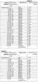
- a multilayer coating comprising 22 layers.
- the coating layer material, layer thickness distribution as well as the index of refraction is listed in Table 1.
- Other coating materials can be used.
- Multilayer coatings comprising more than two materials can be used as well. In the present example the design is optimized for an excitation wavelength of 532 nm.
- Fig. 3 shows schematically the resulting normalized square of the electrical field amplitude as a function of distance from the base 43. Shown as well is the distribution of the index of refraction as a function of the distance from the base 43.
- the square of the electrical field within the interference reflector 45 is oscillating from zero to a local maximum value and back to zero.
- the envelope of the local maxima within the interference reflector is increasing with distance to the base. It is therefore not possible to identify a reflecting surface. Since the excitation light penetrates several wavelenths into the interference reflection, definition of a penetration depth is not useful for defining a reflection surface.
- the areal fluorescent samples 23, 23' is located at or near an antinode of the standing wave which is established above the interference reflector 45 when the stimulating beam is reflected.
- the location of the areal fluorescent samples is especially indicated with an arrow as well as with the broken line.
- maximum fluorescence occurs. Even if the coating thickness is not exactly correct for the excitation wavelength, if the intensity is only 90% or 95% of the peak intensity, the fluorescence signal will still be significantly improved over prior art sample substrates. Variations from the ideal thickness can occur due to sample-to-sample variation and coating variations.
- an optimization strategy of the multilayer coating can be chosen to reach maximum field at the location of the areal fluorescent samples for all excitation wavelengths required. Thus, avoiding the usage of any undesired locations of lower electrical field for any required excitation wavelength.
- the fluorescence imaging system of FIG. 1 could have one or more light sources providing multiple fluorescence excitation wavelengths, either simultaneously or selectably, for different fluorescent sample constituents.
- the nominal optical thickness distribution of the multilayer coating needs and can then be optimized for each of the different excitation wavelengths in parallel for the same multilayer coating.
- Table two shows one example of such a sample substrate optimized for enhancement for the two excitation wavelengths 532nm and 633nm.
- the first excitation wavelength (633nm) is reflected by the dielectric interference layers whereas the second excitation wavelength is reflected by the silver layer.
- the outermost layer of this coating layer system can be used to adjust the electromagnetic field of the first excitation wavelength on the physical surface by adjusting the layer thickness.
- the first layer on the silver coating can be used to adjust the electromagnetic field of the second excitation wavelength by adjusting the layer thickness.
- Table 3 gives an example of a thickness distribution of such a layer system.
- SiO 2 was used as outermost layer. This is the standard material for applying linker chemistry. Linker chemistries are quite sensitive to the materials used on the physical surface of the substrate sample. Therefore different linker chemistries might require outermost layers different from SiO 2 . It is clear that the concept of the invention should not be limited to the use of SiO 2 as outermost layers. In practical examples already TiO 2 and/or Nb 2 O 5 was used. Any other practical optical coating material could be used as well.
- the approach of the present invention can be used due to the absence of any metal layer incorporated.
- the multilayer coating can be in addition optimized to effectively transmit the fluorescent light.
Landscapes
- Physics & Mathematics (AREA)
- Health & Medical Sciences (AREA)
- General Physics & Mathematics (AREA)
- Biochemistry (AREA)
- Chemical & Material Sciences (AREA)
- Analytical Chemistry (AREA)
- Life Sciences & Earth Sciences (AREA)
- General Health & Medical Sciences (AREA)
- Nuclear Medicine, Radiotherapy & Molecular Imaging (AREA)
- Immunology (AREA)
- Pathology (AREA)
- Optics & Photonics (AREA)
- Investigating, Analyzing Materials By Fluorescence Or Luminescence (AREA)
- Optical Measuring Cells (AREA)
Description
- The present invention relates to a sample substrate adapted for use with fluorescence excitation light. Such substrates as plates, slides and cells, are used e.g. in examining, indicating, analyzing or identifying fluorescent, phosphorescent or luminescent sample materials, e.g. tagged molecular biological specimens.
- Fluorescence microscopy is often used in the fields of molecular biology, biochemistry and other life sciences for analyzing biological molecules, including nucleic acids (DNA, RNA) and proteins (enzymes, antigens, etc.) that have been tagged or labeled with fluorescent probes. One such use is DNA diagnostics, such as for gene detection, in which a DNA sample is deposited on and bound to a glass substrate. The bound DNA on the substrate can then be imaged by fluorescence. The fluorescence of a sample was originally assessed by visual inspection through a conventional microscope, but this manual method has proved time-consuming and costly. Many different high-speed automated fluorescence imaging systems are now available.
- An important figure of merit for fluorescence detection and measurement instruments is sensitivity, which is primarily determined by the signal-to-noise ratio (SNR) of the optical imaging system of the instrument. A well-designed imaging system has a signal-to-noise ratio that is limited by its light collection ability and not by internal noise sources. The theoretical SNR of such a system is expressed in terms of the number of photoelectrons at the cathode when using a photomultiplier tube (PMT), which in turn essentially depends upon the number of photons that reach the detector from the area of interest on the sample substrate, the quantum efficiency of the detector, and the number of dark electrons generated by the detector.
- One obvious approach to increasing SNR, and thereby improving sensitivity, is to reduce background noise. Sources of background noise include specular or diffuse reflection of the fluorescence-stimulating laser light from the sample, autofluorescence of the substrate holding the sample, autofluorescence from the optics in the light path of the optical imaging system, stray light, and dark current of the detector. Stray light reaching the detector can be significantly reduced by proper size and placement of apertures in the imaging system. Both stray light and much of the reflected laser light can be rejected, while passing the fluorescent light, by using dichroic and other spectral filters and beamsplitters in the system. Autofluorescence of the optical elements can be reduced by avoiding use of lens cements in the light path, using glass instead of polymeric lenses, or using curved mirrors instead of lenses wherever possible.
- Autofluorescence of the substrate can be reduced by using low fluorescence materials, such as an ultrathin or opaque glass substrate. For example, in
U.S. Pat. No. 5,095,213 Strongin discloses a plastic slide that is rendered opaque and substantially nonfluorescent with a quantity of black carbon powder in the plastic. Another way of handling autofluorescence is to use a pulsed or modulated excitation and to take advantage of the differences in emission decay rates between background fluorescence and specimen fluorescence, as disclosed inU.S. Pat. Nos. 4,877,965 to Dandliker et al . and5,091,653 to Creager et al . - In
U.S. Pat. No. 5,552,272, Bogart discloses an assay system and method for detecting the presence or amount of an analyte of interest. It includes a test substrate with an optically active surface that enhances the color contrast, i.e. differences in the observed wavelength (or combination of wavelengths) of light from the surface, between the presence and absence of the analyte in a sample applied onto the test substrate. In particular, the substrate may comprise a reflective solid optical base, such as a silicon wafer or metallic (e.g., aluminum) base, with an optical thin film coating thereon. The coating may comprise several layers, including for example an attachment layer on the upper surface of the base, and a receptive layer on the upper surface of the attachment layer containing a specific binding partner for the analyte of interest. The total coating thickness is selected to cause incident light to undergo thin film interference upon reflection, such that a specific color is produced. Specifically, the coating material(s) should have an overall thickness of a quarterwave of the unwanted color to be attenuated so that destructive interference of that color will occur. The substrate therefore has a particular background color, which can then be used as a comparative reference against a different observed color when an analyte of interest is present. Both qualitative visual inspection and quantitative instrumented measurement are suggested. Polarization contrast by means of an ellipsometer is also suggested. - One example of the use to which the Bogart approach has been put by Biostar, Inc. of Boulder, Colo., the assignee of the aforementioned patent, is an optical immunoassay (OIA) diagnostic screening test for the rapid detection (in under 30 minutes) of the presence of specific antigens of infectious pathogens in a sample taken from a patient. Commercial products include test kits for group A and group B streptococci and for chlamydia trachomatis. These particular assays are given as examples in the Bogart patent, are described in package inserts for the corresponding Biostar products and are also described in a number of published articles in medical journals. Briefly, they all rely on direct visual detection of a change in the color of light reflection off of the test substrate due to a physical change in the optical thickness of a molecular thin film coating on the substrate surface which results from binding reactions between an immobilized antibody on the test surface and a specific antigen that may be present in a drop of sample liquid applied to the test surface. The original bare test surface has a thin film thickness that results in a predominant visual background gold color when white light is reflected off of the surface. The antigen-antibody binding reaction that occurs when the specific antigen of interest is present in the applied sample results in an increase in the thin film thickness that causes a corresponding change in the color of the test surface from gold to purple. If on the other hand, the antigen is not present in the sample, no binding takes place, the original thin film thickness remains unchanged and the test surface retains its original gold color, indicating a negative result. This diagnostic assay tool is very sensitive and easily interpreted.
- Bogart further discloses, in another embodiment of his approach (FIG. 17 of the aforementioned patent), the use of these substrates for enhanced fluorescence detection. After the analyte of interest has been bound to the surface by reaction with the specific binding partner in the receptive layer of the substrate coating, fluorescent label molecules may be attached to the analyte. In particular, the fluorescent molecules may be attached to any suitably selective and specific receptive material or reagent, such as a secondary antibody, and applied to the surface. The fluorescent labels are thus bound to the analyte of interest on the surface, if present, and immobilized to the surface through the analyte bridge. Directing light of an excitation wavelength onto the surface stimulates fluorescence of any of the label bound to the surface, thereby revealing the presence of the analyte of interest. Because the maximum fluorescence wavelength may not be shifted far enough from the excitation wavelength to be distinguished, the reflective substrate may have an antireflection layer whose thickness is selected to suppress reflection of the excitation wavelength, thereby reducing the background noise reaching the detector. Bogart states that the fluorescent signal generation is not dependent on the film thickness. Though the fluorescence signal S might be increased by increasing the output power of the laser, reflected laser noise will also increase, with possibly little improvement in the resulting SNR.
- In
US 6,008,892 Kain et al disclose a sample substrate which is reflective for the excitation wavelength. This substrate has a transparent coating layer thereon with controlled thickness that has been selected to ensure that a molecular sample placed on top of the coating layer is located at an antinode for the excitation light. In particular, the substrate includes a rigid base with a specularly reflective upper surface. The transparent coating on the upper surface of the base has a thickness selected such that for a particular excitation wavelength of light at normal incidence, the optical path from the top of the coating to the base reflecting surface is substantially an odd multiple (1, 3, 5, etc.) of one-quarter wavelength of the excitation light. The optical path length of the material is defined by the wavelength of light, the index of refraction of the material, and the angle of propagation through the material. In the reflective sample substrate the reflecting surface of the base is at a well defined depth slightly below the physical surface of the base by an amount equal to the sum of the skin (or penetration) depth of the reflective surface material and the optical depth of any surface oxidation on the base. By placing the sample on the coating layer at or near the antinode of the excitation light, maximum fluorescence excitation occurs. A reflective substrate also enhances fluorescence collection by nearly doubling the solid collection angle of a fluorescence imaging microscope system. Thus, the total fluorescence signal is increased, leading to a much improved signal-to-noise ratio. Also, because the coating layer is very thin, there is reduced fluorescence background noise from this material. - As Kain et al describe the base can be made completely of metal or may be composed of a rigid bottom layer with a top metal coating. The metal can be aluminum, silver, gold or rhodium. The transparent coating may be a single layer of dielectric material, such as silica, alumina or a fluoride material (such as MgF2). Alternatively, the transparent coating could be a multilayer coating with the top layer being a chemically reactive material for .binding a specified biological sample constituent thereto.
- Kains concept of applying a transparent quarterwave layer on a reflecting surface is limited to reflectors with rigid surfaces. Here light is not penetrating beneath the physical surface of the reflector or the penetration is limited to at most some nanometers beneath the surface (skin depth). Practically this represents a limitation to metallic surfaces such as metal substrates or metallic coatings.
- As soon as dielectric layers significantly contribute to the reflection, it is difficult to define a penetration depth and the concept of adding a quarterwave layer fails. For example for aluminum mirrors very often additional dielectric layers are used to enhance the reflectivity of the metal which results in so called "pumped metallic mirrors". In this case the dielectric layers are part of the mirror and the last dielectric layer forms the physical surface of the mirror. Light penetrates into such a mirror stack and interference effects together with the metallic reflectivity establish the optical characteristics. Adding an additional quarterwave layer or an odd multiple to such a system very often fails to produce an antinode at the location of fluorescent sample when placed on this layer. In addition in most cases the interference system is disturbed which might result in a drastic decrease of reflectivity.
- However as long as the odd multiple quarterwave condition is fulfilled with respect to the metallic surface it is even possible to enhance fluorescence using the reflectivitiy contribution of the quarterwave layers.
Chaton et al give one example in WO 02/48691 WO 02/48691 - It is an object of the present invention to provide an improved sample substrate which provides increased sample excitation and fluorescence emission.
- The invention is set forth in the appended claims.
- Looking back on the Chaton approach there is one positive effect the authors did not mention: Our investigations showed that using a low index layer as outermost layer results in a field amplitude for 550nm on the surface which is fortunately maximum, 220% more than E2(PW) resulting in an enhancement factor of 2.2. If the authors had used a high index layer as outermost layer the electromagnetic field amplitude would have been minimum.
- Further, with a coating design as used by Chaton et al the reflection band is centered at the design wavelength of 550nm and is 200nm broad. Within the reflection band the reflectivity is increased to slightly below 60%. Because Chaton et al did not take into account the antinode condition, they conclude that the quarterwave stack is effectively enhancing the fluorescence signal for wavelengths between 450nm to 650nm. This wavelength range comprises the wavelengths of the fluorescence materials typically used for fluorescence lables such as CY3 and CY5. Unfortunately only for the design wavelength the antinode condition is well fulfilled. For an excitation wavelength much different from 550nm this condition is not fulfilled. For 450nm the enhancement factor is as low as 0.2 and for 650nm the enhancement factor decreases down to 1.2.
- Thus, the problem is left open by Chaton that it would be desirable to create a sample which provides optimum enhancement for more than one excitation wavelength well separated from each other. Especially for the excitation wavelengths around 532nm-548nm (Cy3) and around 633nm (Cy5) it was still an open question how to realize such a sample substrate.
- Typically there is an inherent difference of signal intensity for Cy3 and Cy5 related for example to differences in affinity of the linker chemistry, resulting in different signal intensities. The question of how to realize for two or more excitation wavelengths approximately the same degree signal intensities was not resolved. The same was valid for considering the possibility to adjust the enhancement factors for two or more excitation wavelengths independently.
- In addition as discussed above, the prior art solutions involved in general interfaces to metallic layers or substrates. Chaton for example restricts the discussion to a silicon substrate. Examples for rigid reflecting surfaces in Kains disclosure always involve metallic surfaces. It was therefore still a problem and was desirable to create a substrate sample providing enhanced fluorescence signal without use of a metallic interface as do Kain et al as well as Chaton et al.
- Thus, the sample substrate according to the present invention has an optical structure which is adapted for enhancing fluorescence detection and imaging. The format of the sample substrate according to the present invention can be adapted to formats which are typically used in the addressed field, such as e.g. the standard format of microtiter plates.
- According to the present invention there is provided at least in some embodiments a sample substrate which has not anymore the disadvantage to base the reflection of the excitation wavelength completely on the reflectivity of a metal surface.
- Thereby, a sample substrate may be realized which provides a maximum enhancement of the fluorescence signal for two or more than two different excitation wavelengths. Thereby and at the sample substrate according to the present invention application-adjusted enhancement factors for two or more excitation wavelengths are provided, whereby such sample substrates as of the present invention are preferably manufactured by the method as was addressed above with its different embodiments.
- One embodiment of the reflective sample substrate according to the present invention has an interference reflector based on a dielectric multilayer coating. The excitation light is reflected with 100% or close to 100%. The resulting electromagnetic field distribution connected to the excitation wavelength outside the sample substrate in the cover region is therefore a standing wave or close to a standing wave with planes of nodes and planes of antinodes. According to the present invention the layers of the interference reflector may have an optimized thickness distribution that has been selected to ensure that an areal fluorescent sample placed on top of the top coating layer is located in the plane of an antinode of the excitation light.
- In this case no quarterwave-thickness requirement for the dielectric layers have to be fulfilled. This gives an additional degree of freedom for the design and the maximum or the desired electromagnetic field can be realized on the physical surface even for two or multiple excitation wavelengths. To be more specific, skipping the condition of using quarterwave layers or odd multiples of quarterwave dielectric layers leads to an additional degree of freedom in the design which can be used to fulfill antinode conditions for two or more excitation wavelengths without the need for compromise as is the case for prior art solutions. This degree of freedom can be used for samples where metallic reflecting interfaces are involved as well as for pure dielectric reflectors.
- The electrical field distribution within such an interference reflector is very different from the field distribution known from specular reflection of a metal surface. An additional layer added on top of the interference reflector can cause a decrease in reflectance. In addition for such an interference reflector it is not possible to define the location of a reflection surface since most of coating layers contribute to the reflection.
- However the inventors found during their studies and experiments that, despite the difficulty to define a reflection surface, it is possible to design an interference reflector in such a way, that there is a maximum field at the physical surface of the reflective sample substrate where the areal fluorescent sample is placed. The design can be found with the help of standard thin film optimization tools, slightly modified to optimize for maximum reflectivity together with maximum field amplitude at the surface of the reflective sample substrate.
- In this case no additional transparent layer is required, no quarterwave-thickness requirement for the dielectric layers have to be fulfilled, so the maximum field can be realized even for two or multiple excitation wavelengths. In addition such a system can be realized without the use of metal layers or a metal substrate at all.
- As already mention such systems can be found using statistical techniques as used typically for optical thin film design, modified to take into account as a part of the optimization target the antinode condition on the physical surface. However the inventors investigated the electromagnetic field distribution within the substrate samples they had optimized with the help of such an optimization procedure. They investigated the sample substrates providing enhanced maximum electromagnetic field intensity at the physical surface of the sample for various designs including prior art solutions as disclosed by Kain et al as well as Chaton et al. They found that the electromagnetic field distribution provides a minimum which is located one quarterwave below the physical surface. This was independent how deep actually the electromagnetic field propagates into the samples. In accordance with the invention, the electromagnetic field needs to provide a minimum which is located approximately one quarterwave beneath the physical surface. This reflects one aspect of the present invention: As long as the substrate sample provides a minimum in the electromagnetic field distribution located approximately one quarterwave beneath the physical surface the eletromagnetic field on the physical surface will be enhanced. The present invention will now be further described by examples and based on figures.
- Therein,
-
FIG. 1 is a schematic drawing of a fluorescence imaging system as typically used. -
FIG. 2 is a close up side section view of a sample substrate of the present invention. -
FIG. 3 is a graph showing the normalized square of the electrical field distribution (E2)/I0 2 versus distance from the base of the sample substrate shown inFig.2 . In addition shown is the distribution of the index of refraction of the multilayer coating. - The sample substrate of the present invention can be used in any of a wide number of possible fluorescence microscope systems, including, for example, those described in
U.S. Pat. Nos. 4,284,897 to Sawamura et al .,5,091,652 to Mathies et al .,5,296,700 to Kumagai ,5,381,224 to Dixon et al ., and5,504,336 to Noguchi , as well asU.S. patent application Ser. Nos. 08/595,355 ,08/616,174 and08/791,684 . - A preferred
fluorescence imaging system 1 for use with the present invention is illustrated inFIG. 1 : Alight source 10, for example a laser, produces anstimulating beam 11. The stimulatingbeam 11 is preferably a collimated beam of monochromatic coherent light. However, a noncoherent source, such as a light emitting diode (LED) could be used and a noncollimated source could be coupled to collimating optics to create a collimated beam. If the stimulatingbeam 11 is not monochromatic, it may be directed through a filter to reduce any unwanted wavelengths. - The stimulating
beam 11 is then directed throughlens systems 12, 12' and abeam splitter 15 onto the surface of thesample substrate 20. Any scanning mechanism that produces a two-dimensional scan may be used to move the substrate along orthogonal axis in plane with the surface of the sample substrate. - The
lens system 12 provides coaxial illumination of the sample substrate with the stimulatingbeam 11. The stimulatingbeam 11 is an excitation beam that stimulates fluorescent light emission from thesample substrate 20 at the illuminated spot: If there are arealfluorescent samples 23, 23' on the illuminated surface of the sample substrate stimulation of detectable fluorescent light results. Thelens system 12 provides as well coaxial collection of the resulting fluorescent light and afluorescent beam 29 is formed. To maximize collection efficiency, it is preferred that thelens system 12 has a large numerical aperture. The fluorescent light is then collected by thelens system 12, acting as a condenser, and directed as a retro-beam back along the incident light path (but in the opposite direction). Since the fluorescent light generally consists of a broad band of wavelengths different from the wavelength(s) of the incident stimulating beam, and since the system should be designed to work with a variety of fluorochromes, the system is preferably largely achromatic and provides correction of chromatic aberrations over a range of wavelengths. Light passing through thelens system 12 impinges upon a photodetector 31, such as a photomultiplier tube (PMT). - Whichever imaging system is used, it should preferably be capable of scanning at high speed over a large scan field with high resolution imaging and minimal optical aberrations. It should provide coaxial illumination and collection with high collection efficiency. An achromatic system with excellent color correction, as well as a system designed for minimizing background noise (including autofluorescence) is preferred.
- With reference to
FIG. 2 , a sample substrate 41 of the present invention comprises abase 43 and aninterference reflector 45 on top of saidbase 43. Theareal fluorescent samples 23, 23' are applied on top of saidinterference reflector 45. - The base 43 could be made of any material that can be coated. For example the base material can be transparent such glass or plastic or it can be metallic such as aluminum. The use of any other rigid bottom layer is possible.
- The
interference reflector 45 comprises a dielectric multilayer coating with at least one highindex coating layer 47 and at least one lowindex coating layer 49. - As coating materials for example Nb2O5, SiO2, aluminum oxide, magnesium oxide, oxides of the groups VIb, Vb; IVb, as well as scandium, yttrium, calcium, strontium, zinc, iron, indium, tin, cerium, holmium, as well as oxide of mixtures or alloys of these elements and further oxynitrides of the elements Ti, Ta, Zr, Si, Hf, Al, as well as fluorides of the elements Magnesium, Barium, Strontium, Calcium, the rare earths and lead can be used.
- The layers may be coated for example by one of the following methods: thermal and/or electron beam vapor deposition, replication, transfer, film deposition, by processes of the CVD type (LPCVD, PECVD etc.) or of the PVD type such as sputtering, i.e. DC magnetron sputtering. Ion assisted deposition processes can be used as well as the sol-gel process. The layers may transferred onto the base by one of the following methods: bonding and molecular adhesion.
- The top layer of the
interference reflector 45 is not necessarily an inert material, but could be biologically active so as to bind with the sample material or a particular constituent of the sample. - In order to maximize the fluorescent emission by maximizing the electrical field at the location of the areal fluorescent sample, the layer thickness distribution of the multilayer coating comprised in the
interference reflector 45 is to be optimized. - The optimization of the multilayer coating design can be done by applying one of the well known optical thin film calculation and optimization techniques. In most cases these techniques are based on minimizing a merit function which measures the distance of the spectral characteristics of the actual thin film design to the target characteristics. Within a slight modification of the standard process the merit function can be modified in such a way that it comprises a term which is addressing the distance of the square of the electrical field to a desired value, which equals in the present case the maximum value of the standing wave.
- In order to correctly determine the proper coating thickness distribution and/or index distribution, the incident angle of the excitation light, the polarization and the refractive indices of the cover medium, of the coating material and of substrate must be taken into account.
- With such an optimization method it is as well possible to design thin film stacks which meet the requirements of maximum field at the location of the
areal fluorescent samples 23, 23' for excitations at two or more excitation wavelengths with the same multilayer coating. It is therefore not necessary to compromise thicknesses to match the desired wavelengths. - The sample substrate 41 is designed to work with any fluorescence imaging system, for example like that shown in
FIG. 1 . The sample substrate 41 according to the present invention is constructed to maximize fluorescent emission and collection without having to increase the power of the laser beam and without having to change the objective or other optics in the system other than the substrate 41 itself. - As an example a multilayer coating is given comprising 22 layers. The coating layer material, layer thickness distribution as well as the index of refraction is listed in Table 1. For this example each individual layer thickness is designed using Nb2O5 (n=2.3) as material with a high optical refractive index and SiO2 (n=1.48) as a material with a low optical refractive index. Other coating materials can be used. Multilayer coatings comprising more than two materials can be used as well. In the present example the design is optimized for an excitation wavelength of 532 nm.
-
Fig. 3 shows schematically the resulting normalized square of the electrical field amplitude as a function of distance from thebase 43. Shown as well is the distribution of the index of refraction as a function of the distance from thebase 43. As can be seen inFig. 3 the square of the electrical field within theinterference reflector 45 is oscillating from zero to a local maximum value and back to zero. The envelope of the local maxima within the interference reflector is increasing with distance to the base. It is therefore not possible to identify a reflecting surface. Since the excitation light penetrates several wavelenths into the interference reflection, definition of a penetration depth is not useful for defining a reflection surface. - As seen in
FIG. 3 , in case the proper coating thickness is provided, theareal fluorescent samples 23, 23' is located at or near an antinode of the standing wave which is established above theinterference reflector 45 when the stimulating beam is reflected. The location of the areal fluorescent samples is especially indicated with an arrow as well as with the broken line. With maximum excitation, maximum fluorescence occurs. Even if the coating thickness is not exactly correct for the excitation wavelength, if the intensity is only 90% or 95% of the peak intensity, the fluorescence signal will still be significantly improved over prior art sample substrates. Variations from the ideal thickness can occur due to sample-to-sample variation and coating variations. - Further, if two or more different excitation wavelengths are to be used with the same substrate sample, an optimization strategy of the multilayer coating can be chosen to reach maximum field at the location of the areal fluorescent samples for all excitation wavelengths required. Thus, avoiding the usage of any undesired locations of lower electrical field for any required excitation wavelength.
- The fluorescence imaging system of
FIG. 1 could have one or more light sources providing multiple fluorescence excitation wavelengths, either simultaneously or selectably, for different fluorescent sample constituents. The nominal optical thickness distribution of the multilayer coating needs and can then be optimized for each of the different excitation wavelengths in parallel for the same multilayer coating. - This is illustrated in more detail in the following example:
Here for the two excitation wavelengths Cy5 at 633nm and Cy3 at 532nm the sample substrate should provide enhanced electromagnetic field on the physical surface. In order to achieve this the inventors proceed according to the following steps: - Designing of a first layer system, reflecting a first wavelength range (620nm-650nm) and transmitting a second wavelength range (520nm-550nm), thereby taking care that the outermost layer is an SiO2 layer.
- Adjusting the outermost layer in such a way, that the square amplitude electromagnetic field for the first excitation wavelength (633nm) on the physical surface of the layer system is almost four times as high as the square of the amplitude electromagnetic field of the incoming propagating plane wave.
- With this the electromagnetic field conditions for the first excitation wavelength are optimum on the surface. The layer thicknesses for this first layer system are now fixed.
- Placing an intermediate layer system between substrate and adjusting the layer thicknesses in order to reflect the second wavelength range.
- Adjusting the thickness of the layer of the intermediate layer system which is adjacent to the first layer system in such a way, that the square amplitude electromagnetic field for the second excitation wavelength (532nm) on the physical surface of the layer system is almost four times as high as the square of the amplitude electromagnetic field of the incoming propagating plane wave.
- With this the electromagnetic field conditions for the second excitation wavelength as well as for the first excitation wavelength are optimum on the surface.
- Table two shows one example of such a sample substrate optimized for enhancement for the two excitation wavelengths 532nm and 633nm.
- Because of this possibility it can be even in the case of the existence of a well defined reflective surface (for example a metallic surface) of advantage to skip the quarterwave condition and to use a dielectric multilayer coating stack and the optimization process as described above to realize maximum fields at the location of the areal fluorescent samples for one more than one excitation wavelength.
- This is illustrated in more detail in the following example:
The first excitation wavelength (633nm) is reflected by the dielectric interference layers whereas the second excitation wavelength is reflected by the silver layer. The outermost layer of this coating layer system can be used to adjust the electromagnetic field of the first excitation wavelength on the physical surface by adjusting the layer thickness. The first layer on the silver coating can be used to adjust the electromagnetic field of the second excitation wavelength by adjusting the layer thickness. Table 3 gives an example of a thickness distribution of such a layer system. - In the examples always SiO2 was used as outermost layer. This is the standard material for applying linker chemistry. Linker chemistries are quite sensitive to the materials used on the physical surface of the substrate sample. Therefore different linker chemistries might require outermost layers different from SiO2. It is clear that the concept of the invention should not be limited to the use of SiO2 as outermost layers. In practical examples already TiO2 and/or Nb2O5 was used. Any other practical optical coating material could be used as well.
- Additionally, in case the fluorescent emission is be detected from the backside of the substrate, the approach of the present invention can be used due to the absence of any metal layer incorporated. In this case the multilayer coating can be in addition optimized to effectively transmit the fluorescent light.
Claims (28)
- A sample substrate (41) adapted for use with fluorescence excitation light with a first wavelength, comprising a base (43) and a reflector, the reflector comprising a reflecting multilayer interference coating (45) with at least two layers (47, 49) and wherein thicknesses of the layers ensures that any fluorescence sample material disposed on top of said multilayer interference coating is located near an antinode of a standing wave formed by the excitation light with said first wavelength incident on said substrate, characterized in that the substrate is adapted so that an electromagnetic field distribution of said fluorescence excitation light provides a minimum which is located one quarterwave below the physical surface and not all of the layers L fulfill a quarterwave condition:

- The sample substrate according to claim 1 further adapted for use with fluorescence excitation light with at least a second wavelength different from the first wavelength, wherein the thicknesses of the layers ensure that the fluorescent sample material disposed on top of said multilayer interference coating is also located near an antinode of a standing wave formed by the excitation light with the second wavelength incident on said substrate.
- The sample substrate according to claim 2, wherein said first wavelength is within the wavelength range of 532nm to 548nm and said second wavelength is around 633nm.
- The sample substrate according to one of the claims 1 to 3 wherein the reflector is metal-free.
- The sample substrate according to one of the claims 1 to 4 wherein the base provides a metallic reflecting surface.
- The sample substrate according to one of the claims 1 to 5 wherein an outermost layer of the reflecting multilayer interference coating is a SiO2 layer.
- The substrate of one of the claims 1 to 6 wherein the multilayer interference coating comprises a first layer system comprising multiple layers and an intermediate layer system comprising multiple layers, the intermediate layer system being disposed between the base and the first layer system.
- The substrate of claim 7 wherein the first layer system transmits light at one of the wavelengths.
- The substrate of claim 7 wherein the intermediate layer system comprises a metal layer disposed on the base and a dielectric layer disposed on the metal layer.
- The substrate of claim 9 wherein the metal layer is one metal of the group comprising silver, gold, aluminum, chromium, platinum and any alloys of these metals.
- The substrate of one of claims to 10 wherein the multilayer interference coating comprises dielectric layers having alternately relatively higher and lower refractive indices such that an outermost layer is one of the layers having a relatively lower refractive index.
- The substrate of claim 11 wherein the layers comprise at least one of Nb2O5, SiO2, aluminum oxide, magnesium oxide; oxides of the groups VIb, Vb, IVb, scandium, yttrium, calcium, strontium, zinc, iron, indium, tin, cerium, or holmium; oxides of mixtures or alloys of scandium, yttrium, calcium, strontium, zinc, iron, indium, tin, cerium, or holmium; and oxynitrides of Ti, Ta, Zr, Si, Hf, or Al; fluorides of magnesium, barium, strontium, calcium, rare earths, and lead.
- The substrate of claim 11 wherein the layers comprise Nb2O5 and SiO2.
- The substrate of one of claims 1 to 13 further comprising a linking coating disposed on an outermost layer of the reflector.
- The substrate of claim 14 wherein the linking coating layer is biologically active.
- The substrate of one of claims 1 to 15 wherein the base is rigid.
- The substrate of one of claims 1 to 16 wherein the base comprises one of glass, plastic, metal, or semiconductor material.
- A method of manufacturing a sample substrate according to any of the previous claims comprising:• selecting layers of the at least two layers of the multilayer interference coating for reflecting the first wavelength of the light; and• determining thicknesses of the layers of the at least two layers.
- The method of claim 18, further comprising• selecting layers of an intermediate layer system of a further multilayer coating for reflecting a second wavelength of the light;• depositing the intermediate layer system between a base and said at least two layers.
- The method of claim 19 further comprising the step of determining the thicknesses of the layers and refraction indices of the layers so as to provide a minimum in the electromagnetic field distribution located approximately one quarter wavelength beneath a physical surface of the substrate.
- The method of one of claims 19 or 20 wherein the at least two layers are selected to transmit light at the second wavelength.
- The method of one of claims 18 to 21 wherein the step of determining the thicknesses of the at least two layers comprises selecting a thickness of an outermost layer to provide a desired enhancement factor at the first wavelength.
- The method of claim 19 wherein a step of determining the thicknesses of the layers of the intermediate layer system comprises selecting a thickness of an outermost layer to provide a desired enhancement factor at the second wavelength.
- The method of one of claims 19 to 23 wherein the step of depositing the intermediate layer system comprises depositing a metal layer on the base and depositing a dielectric layer on the metal layer.
- The method of one of claims 19 to 24 further comprising the step of depositing a linking coating on the at least two layers.
- Use of the sample substrate according to one of claims 1 to 17 in bioanalysis systems.
- A fluorescence imaging system comprising a sample substrate according to one of claims 1 to 17 and a light source directed to a sample material on said sample substrate, said light including the fluorescence excitation wavelength and being particular to a specified fluorescent constituent of said sample material.
- A laser scanner comprising a fluorescence imaging system according to claim 27.
Applications Claiming Priority (3)
| Application Number | Priority Date | Filing Date | Title |
|---|---|---|---|
| US47539503P | 2003-06-03 | 2003-06-03 | |
| US53987204P | 2004-01-28 | 2004-01-28 | |
| PCT/CH2004/000340 WO2004106902A1 (en) | 2003-06-03 | 2004-06-03 | Optical substrate for enhanced detectability of fluorescence |
Publications (2)
| Publication Number | Publication Date |
|---|---|
| EP1629266A1 EP1629266A1 (en) | 2006-03-01 |
| EP1629266B1 true EP1629266B1 (en) | 2023-07-26 |
Family
ID=33493414
Family Applications (1)
| Application Number | Title | Priority Date | Filing Date |
|---|---|---|---|
| EP04735866.8A Expired - Lifetime EP1629266B1 (en) | 2003-06-03 | 2004-06-03 | Optical substrate for enhanced detectability of fluorescence |
Country Status (6)
| Country | Link |
|---|---|
| US (2) | US7227633B2 (en) |
| EP (1) | EP1629266B1 (en) |
| JP (1) | JP4745220B2 (en) |
| CN (1) | CN1798968B (en) |
| TW (1) | TWI329208B (en) |
| WO (1) | WO2004106902A1 (en) |
Families Citing this family (35)
| Publication number | Priority date | Publication date | Assignee | Title |
|---|---|---|---|---|
| DE10150874A1 (en) * | 2001-10-04 | 2003-04-30 | Zeiss Carl | Optical element and method for its production as well as a lithography device and a method for the production of a semiconductor component |
| US7688440B2 (en) * | 2005-01-27 | 2010-03-30 | Prescient Medical, Inc. | Raman spectroscopic test strip systems |
| US9599611B2 (en) | 2005-04-25 | 2017-03-21 | Trustees Of Boston University | Structured substrates for optical surface profiling |
| CN101278186A (en) * | 2005-10-03 | 2008-10-01 | 皇家飞利浦电子股份有限公司 | Biosensors with Improved Sensitivity |
| WO2008028160A2 (en) * | 2006-09-01 | 2008-03-06 | Pacific Biosciences Of California, Inc. | Substrates, systems and methods for analyzing materials |
| US8207509B2 (en) | 2006-09-01 | 2012-06-26 | Pacific Biosciences Of California, Inc. | Substrates, systems and methods for analyzing materials |
| US7988918B2 (en) | 2007-11-01 | 2011-08-02 | Complete Genomics, Inc. | Structures for enhanced detection of fluorescence |
| US9551026B2 (en) | 2007-12-03 | 2017-01-24 | Complete Genomincs, Inc. | Method for nucleic acid detection using voltage enhancement |
| DK3629011T3 (en) | 2008-09-16 | 2024-01-29 | Pacific Biosciences California Inc | INTEGRATED OPTICAL DEVICE |
| US8994946B2 (en) | 2010-02-19 | 2015-03-31 | Pacific Biosciences Of California, Inc. | Integrated analytical system and method |
| EP3460458B1 (en) | 2010-02-19 | 2021-08-11 | Pacific Biosciences of California, Inc. | A method for nucleic acid sequencing |
| JP2013524214A (en) * | 2010-03-29 | 2013-06-17 | アナロジック コーポレイション | Photodetection system and / or photodetection method |
| JP5609729B2 (en) * | 2011-03-18 | 2014-10-22 | 横河電機株式会社 | Microscope device, observation method and sample mounting mechanism |
| US10837879B2 (en) | 2011-11-02 | 2020-11-17 | Complete Genomics, Inc. | Treatment for stabilizing nucleic acid arrays |
| CN102621117B (en) * | 2012-03-09 | 2014-03-12 | 福建师范大学 | Living cell laser scanning co-focusing microscope imaging system |
| US9372308B1 (en) | 2012-06-17 | 2016-06-21 | Pacific Biosciences Of California, Inc. | Arrays of integrated analytical devices and methods for production |
| US9335206B2 (en) | 2012-08-30 | 2016-05-10 | Kla-Tencor Corporation | Wave front aberration metrology of optics of EUV mask inspection system |
| EP2936222B1 (en) | 2012-12-18 | 2019-07-03 | Pacific Biosciences Of California, Inc. | An optical analytical device |
| EP2959283B1 (en) | 2013-02-22 | 2022-08-17 | Pacific Biosciences of California, Inc. | Integrated illumination of optical analytical devices |
| KR102579730B1 (en) | 2014-02-27 | 2023-09-19 | 인튜어티브 서지컬 오퍼레이션즈 인코포레이티드 | System and method for specular reflection detection and reduction |
| DE112015003040T5 (en) * | 2014-06-27 | 2017-03-23 | Keyence Corporation | Photoelectric multi-wavelength meter, confocal meter, interference meter and colorimeter |
| CN107003241B (en) | 2014-08-27 | 2022-01-11 | 加利福尼亚太平洋生物科学股份有限公司 | Integrated analytical device array |
| US10487356B2 (en) | 2015-03-16 | 2019-11-26 | Pacific Biosciences Of California, Inc. | Integrated devices and systems for free-space optical coupling |
| US11983790B2 (en) | 2015-05-07 | 2024-05-14 | Pacific Biosciences Of California, Inc. | Multiprocessor pipeline architecture |
| EP4425153A3 (en) | 2015-06-12 | 2024-11-20 | Pacific Biosciences Of California, Inc. | Integrated target waveguide devices and systems for optical coupling |
| EP3353528B1 (en) | 2015-09-22 | 2023-11-29 | Trustees of Boston University | Multiplexed phenotyping of nanovesicles |
| EP3411713B1 (en) | 2016-02-05 | 2021-06-30 | NanoView Biosciences, Inc. | Detection of exosomes having surface markers |
| DE102016103339A1 (en) * | 2016-02-25 | 2017-08-31 | Fraunhofer-Gesellschaft zur Förderung der angewandten Forschung e.V. | Optical coating and method of making an optical coating with reduced light scattering |
| CN106645086A (en) * | 2016-12-22 | 2017-05-10 | 西安邮电大学 | Preparation method of fractal precious metal nanostructure enhanced spectrum substrate |
| US10859505B2 (en) * | 2018-01-26 | 2020-12-08 | Gemological Institute Of America, Inc. (Gia) | Fluorescence box for gemological applications |
| TWI660218B (en) * | 2018-02-22 | 2019-05-21 | 致茂電子股份有限公司 | Automatic fluorescence detection system |
| US12510462B2 (en) | 2018-06-01 | 2025-12-30 | Unchained Labs | Compositions, systems, and methods for enhanced label-free and fluorescence-based detection of nanoparticles |
| AU2021222009A1 (en) | 2020-02-18 | 2022-09-15 | Pacific Biosciences Of California, Inc. | Highly multiplexed nucleic acid sequencing systems |
| WO2022053971A1 (en) * | 2020-09-09 | 2022-03-17 | Ecole Polytechnique Federale De Lausanne (Epfl) | Measurement device or biochip including an optical microcavity |
| US12535417B2 (en) | 2021-05-04 | 2026-01-27 | Pacific Biosciences Of California, Inc. | Arrays of integrated analytical devices with reduced-scale unit cell |
Family Cites Families (30)
| Publication number | Priority date | Publication date | Assignee | Title |
|---|---|---|---|---|
| US3858046A (en) * | 1973-06-25 | 1974-12-31 | Hughes Aircraft Co | Catadioptric beamsplitter system |
| US4147409A (en) * | 1976-11-22 | 1979-04-03 | Optical Coating Laboratory, Inc. | Laser reflector with reduced electric field intensity |
| JPS53135660A (en) * | 1977-04-30 | 1978-11-27 | Olympus Optical Co Ltd | Fluorescent photometric microscope using laser light |
| DE3109653A1 (en) * | 1980-03-31 | 1982-01-28 | Jenoptik Jena Gmbh, Ddr 6900 Jena | "RESONANCE ABSORBER" |
| US4408825A (en) * | 1980-11-10 | 1983-10-11 | Acton Research Corporation | Vacuum ultraviolet reflectance filter |
| US4627732A (en) * | 1981-05-20 | 1986-12-09 | Raytheon Company | Mode discrimination apparatus |
| US5257140A (en) * | 1982-05-03 | 1993-10-26 | Hughes Aircraft Company | Mirror for infrared and visible wavelength radiation |
| US4877965A (en) * | 1985-07-01 | 1989-10-31 | Diatron Corporation | Fluorometer |
| JPS6435502A (en) * | 1987-07-31 | 1989-02-06 | Nippon Sheet Glass Co Ltd | Reflecting mirror made of multi-layered films |
| US5091653A (en) * | 1987-12-01 | 1992-02-25 | Quantex Corporation | Fiber optic dosimeter using electron trapping materials employing technique for eliminating background fluorescence |
| US5095213A (en) * | 1988-11-03 | 1992-03-10 | Syntex (U.S.A.) Inc. | Method of using an opaque plastic microscope slide for epi-fluorescent microscopy |
| US5091652A (en) * | 1990-01-12 | 1992-02-25 | The Regents Of The University Of California | Laser excited confocal microscope fluorescence scanner and method |
| JP2724563B2 (en) * | 1990-01-14 | 1998-03-09 | 株式会社堀場製作所 | Multilayer interference filter |
| JPH04267202A (en) * | 1991-02-21 | 1992-09-22 | Horiba Ltd | Multi-layer film interference filter |
| JP3082346B2 (en) * | 1991-09-12 | 2000-08-28 | 株式会社ニコン | Fluorescence confocal microscope |
| JP3292935B2 (en) * | 1993-05-18 | 2002-06-17 | 富士写真フイルム株式会社 | Fluorescence spectroscopic image measurement device |
| US5552272A (en) * | 1993-06-10 | 1996-09-03 | Biostar, Inc. | Detection of an analyte by fluorescence using a thin film optical device |
| JPH075311A (en) * | 1993-06-15 | 1995-01-10 | Sony Corp | Optical mirror device |
| US5416583A (en) * | 1993-07-30 | 1995-05-16 | Kearfott Guidance & Navigation Corporation | Quantum well bias mirror for phase modulation in a ring laser gyroscope |
| US5381224A (en) * | 1993-08-30 | 1995-01-10 | A. E. Dixon | Scanning laser imaging system |
| WO1996018205A1 (en) * | 1994-12-08 | 1996-06-13 | Molecular Dynamics, Inc. | Fluorescence imaging system employing a macro scanning objective |
| US5646411A (en) * | 1996-02-01 | 1997-07-08 | Molecular Dynamics, Inc. | Fluorescence imaging system compatible with macro and micro scanning objectives |
| US5847400A (en) * | 1996-02-01 | 1998-12-08 | Molecular Dynamics, Inc. | Fluorescence imaging system having reduced background fluorescence |
| US5694412A (en) * | 1996-04-08 | 1997-12-02 | He Holdings Inc. | Epitaxial visible-light-emitting devices with light extracted through the substrate and method of making same |
| US6008892A (en) * | 1997-05-23 | 1999-12-28 | Molecular Dynamics, Inc. | Optical substrate for enhanced detectability of fluorescence |
| FR2772141B1 (en) * | 1997-12-08 | 2001-10-05 | Commissariat Energie Atomique | LIGHT ABSORBING COVERING WITH HIGH ABSORBING POWER |
| JP2001242083A (en) * | 2000-03-01 | 2001-09-07 | Hamamatsu Photonics Kk | Light intensifying method, light intensifying device, fluorometry using it, and fluorometer |
| FR2813121A1 (en) * | 2000-08-21 | 2002-02-22 | Claude Weisbuch | PERFECTED DEVICE FOR SUPPORTING CHROMOPHORIC ELEMENTS |
| FR2818378B1 (en) * | 2000-12-14 | 2003-06-13 | Commissariat Energie Atomique | LOW BANDWIDTH BROADBAND FLUORESCENCE REINFORCING DEVICE AND BIOLOGICAL OR CHEMICAL OPTICAL SENSOR USING THE SAME |
| GB0122286D0 (en) * | 2001-09-14 | 2001-11-07 | Scient Generics Ltd | Optical coatings for high-throughput laboratory consumables |
-
2004
- 2004-06-01 TW TW093115645A patent/TWI329208B/en not_active IP Right Cessation
- 2004-06-02 US US10/858,792 patent/US7227633B2/en not_active Expired - Lifetime
- 2004-06-03 EP EP04735866.8A patent/EP1629266B1/en not_active Expired - Lifetime
- 2004-06-03 CN CN2004800153868A patent/CN1798968B/en not_active Expired - Lifetime
- 2004-06-03 WO PCT/CH2004/000340 patent/WO2004106902A1/en not_active Ceased
- 2004-06-03 JP JP2006508094A patent/JP4745220B2/en not_active Expired - Fee Related
-
2007
- 2007-04-25 US US11/739,914 patent/US7405819B2/en not_active Expired - Fee Related
Also Published As
| Publication number | Publication date |
|---|---|
| TW200506414A (en) | 2005-02-16 |
| US20070188746A1 (en) | 2007-08-16 |
| CN1798968A (en) | 2006-07-05 |
| US20040247485A1 (en) | 2004-12-09 |
| JP4745220B2 (en) | 2011-08-10 |
| CN1798968B (en) | 2011-08-10 |
| TWI329208B (en) | 2010-08-21 |
| WO2004106902A1 (en) | 2004-12-09 |
| US7405819B2 (en) | 2008-07-29 |
| EP1629266A1 (en) | 2006-03-01 |
| JP2006526768A (en) | 2006-11-24 |
| US7227633B2 (en) | 2007-06-05 |
Similar Documents
| Publication | Publication Date | Title |
|---|---|---|
| US7405819B2 (en) | Optical substrate for enhanced detectability of fluorescence | |
| US6177990B1 (en) | Optical substrate for enhanced detectability of fluorescence | |
| US8287812B2 (en) | Structures for enhanced detection of fluorescence | |
| KR100407821B1 (en) | Waveguide-plasmon resonance sensor using upconversion of active ions and imaging system thereof | |
| US20080240543A1 (en) | Calibration and normalization method for biosensors | |
| WO2005065387A2 (en) | Waveguide comprising scattered light detectable particles | |
| NZ580398A (en) | Grating-based sensor combining label-free binding detection and fluorescence amplification and readout system for sensor | |
| US7349093B2 (en) | Fluorescence measurement apparatus | |
| CN101493411A (en) | Biochip, method for making same, and apparatus applying the biochip | |
| JP2004061211A (en) | Fluorescence detection method and device | |
| EP2076773A1 (en) | Detecting target molecules in a sample | |
| US20050019217A1 (en) | Analytical equipment for determining the chemical structure and/or composition of a plurality of samples and sample holder | |
| US7285789B2 (en) | Optical device for surface-generated fluorescence | |
| US7075641B2 (en) | Biosensor with an arbitrary substrate that can be characterized in photothermal deflection | |
| Burghardt et al. | Around-the-objective total internal reflection fluorescence microscopy |
Legal Events
| Date | Code | Title | Description |
|---|---|---|---|
| PUAI | Public reference made under article 153(3) epc to a published international application that has entered the european phase |
Free format text: ORIGINAL CODE: 0009012 |
|
| 17P | Request for examination filed |
Effective date: 20051015 |
|
| AK | Designated contracting states |
Kind code of ref document: A1 Designated state(s): AT BE BG CH CY CZ DE DK EE ES FI FR GB GR HU IE IT LI LU MC NL PL PT RO SE SI SK TR |
|
| DAX | Request for extension of the european patent (deleted) | ||
| 17Q | First examination report despatched |
Effective date: 20070720 |
|
| RAP1 | Party data changed (applicant data changed or rights of an application transferred) |
Owner name: OC OERLIKON BALZERS AG |
|
| RAP1 | Party data changed (applicant data changed or rights of an application transferred) |
Owner name: OERLIKON TRADING AG, TRUEBBACH |
|
| STAA | Information on the status of an ep patent application or granted ep patent |
Free format text: STATUS: EXAMINATION IS IN PROGRESS |
|
| REG | Reference to a national code |
Ref country code: DE Ref legal event code: R079 Free format text: PREVIOUS MAIN CLASS: G01N0021640000 Ipc: G01N0021030000 Ref country code: DE Ref legal event code: R079 Ref document number: 602004055150 Country of ref document: DE Free format text: PREVIOUS MAIN CLASS: G01N0021640000 Ipc: G01N0021030000 |
|
| RIC1 | Information provided on ipc code assigned before grant |
Ipc: G02B 5/28 20060101ALI20221118BHEP Ipc: G01N 21/64 20060101ALI20221118BHEP Ipc: G01N 21/03 20060101AFI20221118BHEP |
|
| GRAP | Despatch of communication of intention to grant a patent |
Free format text: ORIGINAL CODE: EPIDOSNIGR1 |
|
| STAA | Information on the status of an ep patent application or granted ep patent |
Free format text: STATUS: GRANT OF PATENT IS INTENDED |
|
| INTG | Intention to grant announced |
Effective date: 20230217 |
|
| GRAS | Grant fee paid |
Free format text: ORIGINAL CODE: EPIDOSNIGR3 |
|
| RAP3 | Party data changed (applicant data changed or rights of an application transferred) |
Owner name: OERLIKON SURFACE SOLUTIONS AG, PFAEFFIKON |
|
| GRAA | (expected) grant |
Free format text: ORIGINAL CODE: 0009210 |
|
| STAA | Information on the status of an ep patent application or granted ep patent |
Free format text: STATUS: THE PATENT HAS BEEN GRANTED |
|
| REG | Reference to a national code |
Ref country code: DE Ref legal event code: R081 Ref document number: 602004055150 Country of ref document: DE Owner name: OERLIKON SURFACE SOLUTIONS AG, PFAEFFIKON, CH Free format text: FORMER OWNER: UNAXIS BALZERS AG, BALZERS, LI |
|
| AK | Designated contracting states |
Kind code of ref document: B1 Designated state(s): AT BE BG CH CY CZ DE DK EE ES FI FR GB GR HU IE IT LI LU MC NL PL PT RO SE SI SK TR |
|
| REG | Reference to a national code |
Ref country code: CH Ref legal event code: EP |
|
| REG | Reference to a national code |
Ref country code: DE Ref legal event code: R096 Ref document number: 602004055150 Country of ref document: DE |
|
| REG | Reference to a national code |
Ref country code: IE Ref legal event code: FG4D |
|
| REG | Reference to a national code |
Ref country code: NL Ref legal event code: MP Effective date: 20230726 |
|
| REG | Reference to a national code |
Ref country code: AT Ref legal event code: MK05 Ref document number: 1592459 Country of ref document: AT Kind code of ref document: T Effective date: 20230726 |
|
| PG25 | Lapsed in a contracting state [announced via postgrant information from national office to epo] |
Ref country code: NL Free format text: LAPSE BECAUSE OF FAILURE TO SUBMIT A TRANSLATION OF THE DESCRIPTION OR TO PAY THE FEE WITHIN THE PRESCRIBED TIME-LIMIT Effective date: 20230726 |
|
| PG25 | Lapsed in a contracting state [announced via postgrant information from national office to epo] |
Ref country code: GR Free format text: LAPSE BECAUSE OF FAILURE TO SUBMIT A TRANSLATION OF THE DESCRIPTION OR TO PAY THE FEE WITHIN THE PRESCRIBED TIME-LIMIT Effective date: 20231027 |
|
| PG25 | Lapsed in a contracting state [announced via postgrant information from national office to epo] |
Ref country code: SE Free format text: LAPSE BECAUSE OF FAILURE TO SUBMIT A TRANSLATION OF THE DESCRIPTION OR TO PAY THE FEE WITHIN THE PRESCRIBED TIME-LIMIT Effective date: 20230726 Ref country code: PT Free format text: LAPSE BECAUSE OF FAILURE TO SUBMIT A TRANSLATION OF THE DESCRIPTION OR TO PAY THE FEE WITHIN THE PRESCRIBED TIME-LIMIT Effective date: 20231127 Ref country code: GR Free format text: LAPSE BECAUSE OF FAILURE TO SUBMIT A TRANSLATION OF THE DESCRIPTION OR TO PAY THE FEE WITHIN THE PRESCRIBED TIME-LIMIT Effective date: 20231027 Ref country code: AT Free format text: LAPSE BECAUSE OF FAILURE TO SUBMIT A TRANSLATION OF THE DESCRIPTION OR TO PAY THE FEE WITHIN THE PRESCRIBED TIME-LIMIT Effective date: 20230726 |
|
| PG25 | Lapsed in a contracting state [announced via postgrant information from national office to epo] |
Ref country code: PL Free format text: LAPSE BECAUSE OF FAILURE TO SUBMIT A TRANSLATION OF THE DESCRIPTION OR TO PAY THE FEE WITHIN THE PRESCRIBED TIME-LIMIT Effective date: 20230726 |
|
| PG25 | Lapsed in a contracting state [announced via postgrant information from national office to epo] |
Ref country code: ES Free format text: LAPSE BECAUSE OF FAILURE TO SUBMIT A TRANSLATION OF THE DESCRIPTION OR TO PAY THE FEE WITHIN THE PRESCRIBED TIME-LIMIT Effective date: 20230726 |
|
| REG | Reference to a national code |
Ref country code: DE Ref legal event code: R097 Ref document number: 602004055150 Country of ref document: DE |
|
| PG25 | Lapsed in a contracting state [announced via postgrant information from national office to epo] |
Ref country code: RO Free format text: LAPSE BECAUSE OF FAILURE TO SUBMIT A TRANSLATION OF THE DESCRIPTION OR TO PAY THE FEE WITHIN THE PRESCRIBED TIME-LIMIT Effective date: 20230726 Ref country code: ES Free format text: LAPSE BECAUSE OF FAILURE TO SUBMIT A TRANSLATION OF THE DESCRIPTION OR TO PAY THE FEE WITHIN THE PRESCRIBED TIME-LIMIT Effective date: 20230726 Ref country code: EE Free format text: LAPSE BECAUSE OF FAILURE TO SUBMIT A TRANSLATION OF THE DESCRIPTION OR TO PAY THE FEE WITHIN THE PRESCRIBED TIME-LIMIT Effective date: 20230726 Ref country code: DK Free format text: LAPSE BECAUSE OF FAILURE TO SUBMIT A TRANSLATION OF THE DESCRIPTION OR TO PAY THE FEE WITHIN THE PRESCRIBED TIME-LIMIT Effective date: 20230726 Ref country code: CZ Free format text: LAPSE BECAUSE OF FAILURE TO SUBMIT A TRANSLATION OF THE DESCRIPTION OR TO PAY THE FEE WITHIN THE PRESCRIBED TIME-LIMIT Effective date: 20230726 Ref country code: SK Free format text: LAPSE BECAUSE OF FAILURE TO SUBMIT A TRANSLATION OF THE DESCRIPTION OR TO PAY THE FEE WITHIN THE PRESCRIBED TIME-LIMIT Effective date: 20230726 |
|
| PG25 | Lapsed in a contracting state [announced via postgrant information from national office to epo] |
Ref country code: IT Free format text: LAPSE BECAUSE OF FAILURE TO SUBMIT A TRANSLATION OF THE DESCRIPTION OR TO PAY THE FEE WITHIN THE PRESCRIBED TIME-LIMIT Effective date: 20230726 |
|
| PLBE | No opposition filed within time limit |
Free format text: ORIGINAL CODE: 0009261 |
|
| STAA | Information on the status of an ep patent application or granted ep patent |
Free format text: STATUS: NO OPPOSITION FILED WITHIN TIME LIMIT |
|
| REG | Reference to a national code |
Ref country code: DE Ref legal event code: R071 Ref document number: 602004055150 Country of ref document: DE |
|
| REG | Reference to a national code |
Ref country code: CH Ref legal event code: PL |
|
| REG | Reference to a national code |
Ref country code: BE Ref legal event code: MK Effective date: 20240603 |
|
| 26N | No opposition filed |
Effective date: 20240429 |
|
| PG25 | Lapsed in a contracting state [announced via postgrant information from national office to epo] |
Ref country code: SI Free format text: LAPSE BECAUSE OF FAILURE TO SUBMIT A TRANSLATION OF THE DESCRIPTION OR TO PAY THE FEE WITHIN THE PRESCRIBED TIME-LIMIT Effective date: 20230726 |
|
| PG25 | Lapsed in a contracting state [announced via postgrant information from national office to epo] |
Ref country code: IE Free format text: LAPSE BECAUSE OF EXPIRATION OF PROTECTION Effective date: 20240603 |
|
| PG25 | Lapsed in a contracting state [announced via postgrant information from national office to epo] |
Ref country code: IE Free format text: LAPSE BECAUSE OF EXPIRATION OF PROTECTION Effective date: 20240603 |
|
| PG25 | Lapsed in a contracting state [announced via postgrant information from national office to epo] |
Ref country code: BG Free format text: LAPSE BECAUSE OF FAILURE TO SUBMIT A TRANSLATION OF THE DESCRIPTION OR TO PAY THE FEE WITHIN THE PRESCRIBED TIME-LIMIT Effective date: 20230726 |
|
| PG25 | Lapsed in a contracting state [announced via postgrant information from national office to epo] |
Ref country code: BG Free format text: LAPSE BECAUSE OF FAILURE TO SUBMIT A TRANSLATION OF THE DESCRIPTION OR TO PAY THE FEE WITHIN THE PRESCRIBED TIME-LIMIT Effective date: 20230726 |
|
| REG | Reference to a national code |
Ref country code: GB Ref legal event code: PE20 Expiry date: 20240602 |
|
| PG25 | Lapsed in a contracting state [announced via postgrant information from national office to epo] |
Ref country code: GB Free format text: LAPSE BECAUSE OF EXPIRATION OF PROTECTION Effective date: 20240602 |