EP1626268B1 - Method and apparatus for detecting wear in components of high voltage electrical equipment - Google Patents
Method and apparatus for detecting wear in components of high voltage electrical equipment Download PDFInfo
- Publication number
- EP1626268B1 EP1626268B1 EP05254930A EP05254930A EP1626268B1 EP 1626268 B1 EP1626268 B1 EP 1626268B1 EP 05254930 A EP05254930 A EP 05254930A EP 05254930 A EP05254930 A EP 05254930A EP 1626268 B1 EP1626268 B1 EP 1626268B1
- Authority
- EP
- European Patent Office
- Prior art keywords
- component
- tracer material
- insulating medium
- fluorescent tracer
- electrical
- Prior art date
- Legal status (The legal status is an assumption and is not a legal conclusion. Google has not performed a legal analysis and makes no representation as to the accuracy of the status listed.)
- Expired - Lifetime
Links
Images


Classifications
-
- G—PHYSICS
- G01—MEASURING; TESTING
- G01R—MEASURING ELECTRIC VARIABLES; MEASURING MAGNETIC VARIABLES
- G01R31/00—Arrangements for testing electric properties; Arrangements for locating electric faults; Arrangements for electrical testing characterised by what is being tested not provided for elsewhere
- G01R31/327—Testing of circuit interrupters, switches or circuit-breakers
- G01R31/3271—Testing of circuit interrupters, switches or circuit-breakers of high voltage or medium voltage devices
- G01R31/3272—Apparatus, systems or circuits therefor
- G01R31/3274—Details related to measuring, e.g. sensing, displaying or computing; Measuring of variables related to the contact pieces, e.g. wear, position or resistance
-
- G—PHYSICS
- G01—MEASURING; TESTING
- G01N—INVESTIGATING OR ANALYSING MATERIALS BY DETERMINING THEIR CHEMICAL OR PHYSICAL PROPERTIES
- G01N21/00—Investigating or analysing materials by the use of optical means, i.e. using sub-millimetre waves, infrared, visible or ultraviolet light
- G01N21/62—Systems in which the material investigated is excited whereby it emits light or causes a change in wavelength of the incident light
- G01N21/66—Systems in which the material investigated is excited whereby it emits light or causes a change in wavelength of the incident light electrically excited, e.g. electroluminescence
- G01N21/67—Systems in which the material investigated is excited whereby it emits light or causes a change in wavelength of the incident light electrically excited, e.g. electroluminescence using electric arcs or discharges
-
- H—ELECTRICITY
- H01—ELECTRIC ELEMENTS
- H01H—ELECTRIC SWITCHES; RELAYS; SELECTORS; EMERGENCY PROTECTIVE DEVICES
- H01H1/00—Contacts
- H01H1/0015—Means for testing or for inspecting contacts, e.g. wear indicator
-
- H—ELECTRICITY
- H01—ELECTRIC ELEMENTS
- H01H—ELECTRIC SWITCHES; RELAYS; SELECTORS; EMERGENCY PROTECTIVE DEVICES
- H01H33/00—High-tension or heavy-current switches with arc-extinguishing or arc-preventing means
- H01H33/70—Switches with separate means for directing, obtaining, or increasing flow of arc-extinguishing fluid
- H01H33/7015—Switches with separate means for directing, obtaining, or increasing flow of arc-extinguishing fluid characterised by flow directing elements associated with contacts
- H01H33/7076—Switches with separate means for directing, obtaining, or increasing flow of arc-extinguishing fluid characterised by flow directing elements associated with contacts characterised by the use of special materials
-
- H—ELECTRICITY
- H01—ELECTRIC ELEMENTS
- H01H—ELECTRIC SWITCHES; RELAYS; SELECTORS; EMERGENCY PROTECTIVE DEVICES
- H01H1/00—Contacts
- H01H1/0015—Means for testing or for inspecting contacts, e.g. wear indicator
- H01H2001/0026—Means for testing or for inspecting contacts, e.g. wear indicator wherein one or both contacts contain embedded contact wear signal material, e.g. radioactive material being released as soon as the contact wear reaches the embedded layer
-
- H—ELECTRICITY
- H01—ELECTRIC ELEMENTS
- H01H—ELECTRIC SWITCHES; RELAYS; SELECTORS; EMERGENCY PROTECTIVE DEVICES
- H01H1/00—Contacts
- H01H1/0015—Means for testing or for inspecting contacts, e.g. wear indicator
- H01H2001/0031—Means for testing or for inspecting contacts, e.g. wear indicator by analysing radiation emitted by arc or trace material
-
- H—ELECTRICITY
- H01—ELECTRIC ELEMENTS
- H01H—ELECTRIC SWITCHES; RELAYS; SELECTORS; EMERGENCY PROTECTIVE DEVICES
- H01H9/00—Details of switching devices, not covered by groups H01H1/00 - H01H7/00
- H01H9/0005—Tap change devices
- H01H2009/0061—Monitoring tap change switching devices
-
- H—ELECTRICITY
- H01—ELECTRIC ELEMENTS
- H01H—ELECTRIC SWITCHES; RELAYS; SELECTORS; EMERGENCY PROTECTIVE DEVICES
- H01H33/00—High-tension or heavy-current switches with arc-extinguishing or arc-preventing means
- H01H33/70—Switches with separate means for directing, obtaining, or increasing flow of arc-extinguishing fluid
- H01H33/7015—Switches with separate means for directing, obtaining, or increasing flow of arc-extinguishing fluid characterised by flow directing elements associated with contacts
- H01H33/7023—Switches with separate means for directing, obtaining, or increasing flow of arc-extinguishing fluid characterised by flow directing elements associated with contacts characterised by an insulating tubular gas flow enhancing nozzle
-
- H—ELECTRICITY
- H01—ELECTRIC ELEMENTS
- H01H—ELECTRIC SWITCHES; RELAYS; SELECTORS; EMERGENCY PROTECTIVE DEVICES
- H01H9/00—Details of switching devices, not covered by groups H01H1/00 - H01H7/00
- H01H9/0005—Tap change devices
Definitions
- the invention relates generally to high voltage electrical equipment. More specifically, the invention is directed to detecting wear in components of high voltage electrical equipment that are regularly exposed to electrical arcing.
- Load tap changers, voltage regulators, circuit breakers and switches are used to interrupt power.
- the surfaces of some of their components are eroded by being regularly exposed to electrical arcing and mechanical friction during the course of their normal operation.
- Equipment failure results if these components are allowed to wear out to the extent that their electrical and mechanical integrity is compromised.
- Components most susceptible to erosion are the arcing metal contacts and TEFLON nozzles in sulfur hexafluoride (SF 6 ) gas circuit breakers.
- One approach is installing fiber optic strands into the electrical contacts of the electrical equipment. As the contacts wear, the fiber optic strands become exposed to light emitted from electrical arcing, which may be detected by a photodiode or other sensor placed at the opposite ends of the fiber optic strands. Installing fiber optic strands in electrical contacts is expensive, however, and the fiber optic strands are subject to breakage as a result of mechanical stress.
- Another approach embeds tracer materials at predetermined depths in the electrical contacts or below the surface of a TEFLON nozzle of a SF6 circuit breaker.
- the present invention comprises a method of monitoring a component of an electrical device for wear by exposing a component having a tracer material embedded in it at a predetermined depth to an electrical arc, wearing the component until the tracer material is exposed to the electrical arc, and detecting electromagnetic radiation emitted by the tracer material when the tracer material is exposed to the electrical arc.
- the electromagnetic radiation emitted by the tracer material is distinct from electromagnetic radiation emitted by any other parts of the component; for example, it may have a different wavelength.
- the component is preferably monitored continuously to detect electromagnetic radiation emitted by the tracer material.
- Another embodiment of the present invention comprises a method of manufacturing a component of a device in which an electrical arc may be generated wherein the method involves embedding a tracer material within the component at a predetermined depth.
- Yet another embodiment of the present invention comprises an apparatus for detecting wear in an electrical device in which a tracer material is embedded at a predetermined depth within a component of the electrical device.
- the tracer material emits electromagnetic radiation when the tracer material is exposed to an electrical arc that is distinct from electromagnetic radiation emitted by any other parts of the component; for example, it may have a different wavelength.
- the apparatus preferably includes an electromagnetic detector, such as a photodiode having a narrow bandwidth filter or spectrophotometer, to continuously monitor the component for electromagnetic radiation emitted by the tracer material.
- a fiber optic cable may be used to transmit the electromagnetic radiation to the electromagnetic detector.
- Suitable tracer materials include lithium, cobalt, niobium and rare earth metals, such as yttrium.
- multiple tracer materials may be embedded at multiple pre-determined depths and/or at preselected locations within the component in order to detect the extent and/or location of wearing in the component.
- the present invention provides a method for detecting wear in a component of an electrical device, comprising exposing a component of an electrical device to an electrical arc, wherein the component has a fluorescent tracer material embedded at a predetermined depth; wearing the component such that the fluorescent tracer material is released into an insulating medium surrounding at least a portion of the component; irradiating the insulating medium, thereby causing the fluorescent tracer material to produce fluorescence; and detecting the fluorescence from the fluorescent tracer material.
- the present invention provides a method for manufacturing a component of a device in which an electrical arc may be generated, comprising embedding a fluorescent tracer material in a component of a device at a predetermined depth.
- the present invention also provides a system for detecting wear in an electrical device, comprising a component of a device that is exposed to an electrical arc, wherein the component is insulated by an insulating medium; a fluorescent tracer material embedded at a predetermined depth in the component; and a detector configured to irradiate the fluorescent tracer material and to detect fluorescence produced by the fluorescent tracer material.
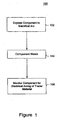
- Figure 1 is a flowchart of a method for detecting wear in a component of an electrical device in accordance with an embodiment of the invention
- Figure 2 is a schematic of an apparatus for detecting wear in a component of an electrical device in accordance with an embodiment of the invention
- Figure 3 is a schematic of the apparatus in Figure 2 at a later time after the component has been worn to expose a tracer material
- Figure 4 is a schematic of an apparatus for detecting two amounts of wear in a component of an electrical device in accordance with an alternate embodiment of the invention
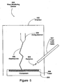
- Figure 5 is a schematic of an apparatus for detecting wear in a component of an electrical device in accordance with an alternate embodiment of the invention
- Figure 6 is a diagram showing a cross-sectional view of components of a load tap changer in accordance with an embodiment of the invention.
- Figure 7 is a diagram showing a partially cut away cross-sectional view of components of a circuit breaker in accordance with an embodiment of the invention.
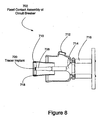
- Figure 8 is a diagram showing a partially cut away cross-sectional view of the fixed contact assembly of a circuit breaker in accordance with an embodiment of the invention.
- Figure 9 is a diagram showing a partially cut away cross-sectional view of the moving contact assembly of a circuit breaker in accordance with an embodiment of the invention.
- Figure 10 provides a schematic of an apparatus for detecting wear in a component of an electrical device in accordance with another embodiment of the invention.
- Figure 11 provides a schematic of an apparatus for detecting wear in a component of an electrical device in accordance with yet another embodiment of the invention.
- FIG. 1 shows a flowchart 100 for detecting wear in a component of an electrical device in accordance with an embodiment of the present invention.
- the component which contains a tracer material embedded in it at a predetermined depth, is exposed to an electrical arc.
- the component wears as a result of the exposure to the electrical arc or other causes, such as mechanical friction.
- the component is continuously monitored for electromagnetic radiation from the tracer material in step 106; the tracer material emits electromagnetic radiation when the component is sufficiently worn so that the embedded tracer material itself is exposed to the electric arc.
- the tracer material is embedded in the component preferably during the manufacturing of the component, but the tracer material may also be embedded in existing components after they have been manufactured.
- Figures 2 and 3 are schematics of an apparatus 200 for detecting wear in a component 202 of an electrical device in accordance with an embodiment of the present invention.
- Figure 2 illustrates the apparatus 200 at an initial time
- Figure 3 illustrates the apparatus at a later time.
- a component 202 of an electrical device (not shown) has a tracer material 204 embedded in it at a predetermined depth.
- the component 202 is exposed to an electrical arc 206 that is generated by an electrical arcing element 208.
- the high temperature of the electrical arc 206 causes the portion of the component 202 that is exposed to the electrical arc 206 to emit electromagnetic radiation 207 that is continuously monitored by an electromagnetic detector, which may be a photodiode 210 or any other suitable detector for electromagnetic radiation (such as a spectrophotometer).
- an electromagnetic detector which may be a photodiode 210 or any other suitable detector for electromagnetic radiation (such as a spectrophotometer).
- a narrow band filter 212 is placed between the photodiode 210 and the component 202 of the electrical device so that the photodiode 210 is allowed to detect electromagnetic radiation having a wavelength in the narrow band that can pass through the narrow band filter 212.
- the electromagnetic radiation 207 has not been transmitted through the narrow band filter 212 because the electromagnetic radiation 207 was not emitted by the tracer material 204.
- the electromagnetic detector is capable of monitoring the component 202 of the electrical device continuously during the operation of the electrical device.
- Figure 3 is a schematic of the apparatus 200 in Figure 2 but at a later time after the component 202 has been worn.
- Figure 3 shows the tracer material 204 on a surface of the component 202, instead of embedded in the component at a predetermined depth.
- the surface of the component 202 has been worn away as a result of exposure to the electrical arc 206 or other causes, such as mechanical friction, so that the tracer material 204 is exposed to the electrical arc 206.
- the high temperature of the electrical arc 206 causes the tracer material 204 to emit electromagnetic radiation 209.
- the tracer material 204 is selected so that when it is exposed to the electrical arc 206, it emits electromagnetic radiation 209 that is distinct from the electromagnetic radiation 207 ( Figure 2 ) emitted by any other parts of the component that are exposed to the electrical arc.
- electromagnetic radiation 209 that is distinct from the electromagnetic radiation 207 ( Figure 2 ) emitted by any other parts of the component that are exposed to the electrical arc.
- lithium which emits red light corresponding to a wavelength of approximately 670.7 nm
- the materials that may be suitable for use as a tracer material in accordance with this invention are lithium, cobalt, niobium and rare earth metals such as yttrium.
- the electromagnetic radiation 209 has been transmitted through the narrow band filter 212 because the electromagnetic radiation 209 was emitted by the tracer material 204.
- the electromagnetic radiation emitted by the tracer material 204 when it is exposed to the electrical arc 206 is detected by a photodiode 210 after the electromagnetic radiation has passed through a narrow band filter 212.
- the narrow band filter removes electromagnetic radiation with a wavelength outside the narrow band that is transmitted by the narrow band filter 212.
- the narrow band filter 212 is selected so that it transmits electromagnetic radiation that is emitted by the tracer material when it is exposed to the electrical arc but not electromagnetic radiation emitted by other parts of the component 202.
- Figure 4 is a schematic of an apparatus 400 for detecting two amounts of wear in a component 202 of an electrical device in accordance with an alternate embodiment of the present invention.
- a first tracer material 402 is embedded at one depth within the component 202 and a second tracer material 404 is embedded at another depth within the component 202.
- the first tracer material 402 and the second tracer material 404 are selected so that when they are exposed to the electrical arc 206, they emit electromagnetic radiation that is distinct from each other as well as from the radiation emitted by any other parts of the component that are exposed to the electrical arc.
- a spectrophotometer 406 analyzes electromagnetic radiation from the component 202 to determine whether the surface of the component 202 has worn to expose either the first tracer material 402 or the second tracer material 404.
- two photodiodes with differing narrow band filters may be used to monitor electromagnetic radiation from the first tracer material 402 and the second tracer material 404.
- Additional tracer materials (not shown) may be imbedded in the component 202 at various depths and/or at different locations in order to estimate the extent and/or location of wear of the component 202 according to which of the tracer materials is exposed to the electrical arc 206.
- FIG. 5 is a schematic of an apparatus 500 for detecting wear in a component 202 of an electrical device in accordance with an alternate embodiment of the present invention.
- an arcing element 208 and a component 202 having an embedded tracer material 204 are placed in an equipment chamber 502 and a fiber optic cable 504 is used to transmit electromagnetic radiation emitted by the component to an electromagnetic detector (not shown) outside the equipment chamber 502.
- FIG. 6 is a cross-sectional view of a diverter switch assembly 600 of a load tap changer in accordance with an embodiment of the invention.
- the diverter switch assembly 600 includes an arcing contact tip assembly 602 at one end of the diverter switch assembly and a compression spring 604 at its opposite end.
- the arcing contact tip assembly 602 may include an elkonite contact 606.
- tracer material 608 is embedded within the elkonite contact 606.
- the tracer material 608 will become exposed to an electrical arc (not shown) after the surface of the elkonite contact 606 is worn away, and an electromagnetic detector (not shown) will detect the distinctive electromagnetic radiation emitted by the tracer material 608.
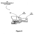
- Figures 7 , 8 and 9 are, respectively, partially cut away cross-sectional views of a circuit breaker 700, the fixed contact assembly 702 of the circuit breaker 700, and the moving contact assembly 708 of the circuit breaker 700 in accordance with an embodiment of the invention.
- Figure 7 shows a circuit breaker 700, comprised of a fixed contact assembly 702 with a fixed contact pin 706, a tank 704, and a moving contact assembly 708.
- Figure 8 shows a fixed contact assembly 702 of a circuit breaker 700, comprised of shielding 710, a multicontact liner and a clamping ring 712, a contact pin holder 714, insulating support 716, a contact crown 718, and a fixed contact pin 706.
- tracer material 720 is embedded within the fixed contact pin 706.
- the tracer material 720 will become exposed to an electrical arc (not shown) after the surface of the fixed contact pin 706 is worn away, and an electromagnetic detector (not shown) will detect the distinctive electromagnetic radiation emitted by the tracer material 720.
- Figure 9 shows a moving contact assembly 708 of a circuit breaker 700, comprised of a main contact 722.
- tracer materials 724 and 726 are embedded within the main contact 722.
- the tracer materials 724 and 726 will become exposed to an electrical arc (not shown) after the surface of the main contact 722 is worn away, and an electromagnetic detector (not shown) will detect the distinctive electromagnetic radiation emitted by the tracer materials 724 and 726.
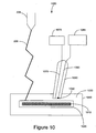
- Figure 10 provides a schematic of an apparatus 1000 for detecting wear in a component of an electrical device in accordance with another embodiment of the invention.
- the tracer material 1010 comprises a fluorescent material.
- the fluorescent material is embedded at a predetermined depth in a component 1020 of an electrical device.
- This embodiment is preferably used when the component 1020 is immersed in an insulating medium 1030, such as a mineral oil.
- the insulating medium preferably surrounds the component 1020 and is contained within a container 1040 or the electrical device within which the component 1020 resides.
- the wear of the component 1020 may be the result of an arc 206 that is discharged from an arcing element 208 or may be the result of mechanical friction.
- the insulating medium 1030 is irradiated or illuminated, thereby exciting the fluorescent tracer material 1010 and causing it to fluoresce.
- a probe 1050 is disposed in the container 1040 or electrical device holding the insulating medium and is used to provide radiation or excitation light to the insulating medium 1030.
- a radiation or electromagnetic radiation source 1075 is connected to the probe by, for example, a fiber optic connection 1070, which supplies radiation to the insulating medium 1030.
- the radiation source 1075 may be any source of light or radiation having a desired wavelength corresponding to the wavelength necessary to cause the fluorescent tracer material 1010 in the insulating medium 1030 to fluoresce.
- the wavelength of the fluorescence is different from the light used to irradiate or illuminate the fluorescent tracer material.
- the fluorescence produced by the fluorescent tracer material 1010 that has been irradiated or illuminated by the radiation from the probe 1050 is also detected by the same probe 1050.
- the probe 1050 also comprises a detector 1055, such as an optical sensor, such as a photodiode, or other suitable device, that may continuously monitor for and detect fluorescence. It should be appreciated that other optical elements, such as filters, may be used in conjunction with the detector 1055 to selectively monitor for specific fluorescence produced by the irradiated fluorescent tracer material 1010 in the insulating medium 1030.
- the detector 1055 is electrically connected by an electrical connector 1060 to a recording device 1065 that will record and analyze the signal provided by the detector 1055 to determine whether the fluorescent tracer material 1010 has been released into the insulating medium 1030, thereby indicating that wear of the component 1020 has progressed to a predetermined amount.
- the detector 1055 may simply be the end of a fiber optic cable that passes received light to an optical monitoring device, such as a spectrophotometer, for analysis (not shown).
- the probe may be permanently positioned within the insulating medium 1030 to irradiate, in-situ, any fluorescent tracer material released into the insulating medium and to detect, in-situ, fluorescence on a continuous, semi-continuous or as-needed basis.
- fluorescence is detected during a time when there is no arcing so as to minimize any interference that may be caused by the arc in detecting the fluorescence.
- the container 1040 may be configured such that the probe 1050 can be inserted only when needed.
- the signal provided by the detector 1055 or by an optical monitoring device, such as a spectrophotometer can also be connected to a computer for data storage and analysis.
- the fluorescent tracer material may be utilized at any desired depth within the component and may be placed at more than one depth within the same component, thereby providing information regarding the rate of deterioration of the component and multiple indications as the component wears.
- the fluorescent tracer material itself may be any fluorescent material; provided that it will either dissolve in, or disperse in, the surrounding insulating medium.
- the fluorescent tracer material will provide enough fluorescence such that, upon dissolving or dispersing in the surrounding insulating medium, such fluorescence can be detected at low concentrations of the fluorescent tracer material in the insulating medium.
- fluorescence from the fluorescent material should be detectable at a concentration of approximately 0.5 ppb of the fluorescent material in the insulating material.
- the fluorescent tracer material upon excitation from a light or energy source, the fluorescent tracer material emits a light ( i . e ., fluorescence) that has a wavelength that is always longer than that of the excitation light (such as ultraviolet or visible light).
- the insulating material is an oil, it is desirable to select a fluorescent tracer material that emits light or fluorescence in the red region of the spectrum to minimize interference from the oil.
- the composition of the fluorescent material may be an organic dye. Any suitable organic dye may be used.
- the organic dye can be a powder or a liquid containing the organic dye powder. If the organic dye is in liquid form, the liquid can be sealed in a container within the electrical component in which it is embedded; however, the container must be capable of rupturing once it is exposed to allow the organic dye to dissolve or disperse into the surrounding insulating medium.
- the organic dye has a high solubility in the insulating medium such as oil, good chemical and thermal stability, a high boiling point, for example, a boiling point greater than approximately 150°C, and the ability to produce a high level of fluorescence.
- the organic dye is a solvent dye, including, for example, azo dyes, which is more soluble in the insulating medium and will not settle out.
- the fluorescent material may also be an inorganic nanocrystal powder.
- the inorganic nanocrystal powder is a semiconductor nanocrystal quantum dot, ranging in a particulate size from approximately 2-10 nm, with a preferred size range of approximately 4-5 nm.
- These types of nanocrystals typically exhibit high fluorescence intensity in a narrow bandwidth, are very chemically and thermally stable, are resistive to fading, and can be excited with a broadband source.
- the nanocrystal powder may be cadmium-tellurium/cadmium sulfide or cadmium-selenium/zinc sulfide, such as EVIDOTS, available from Evident Technology. These specific nanocrystals also emit light in the red region of the spectrum and are prone to less interference from the insulating medium such as oil.
- Figure 11 provides a schematic of an apparatus 1100 for detecting wear in a component of an electrical device in accordance with yet another embodiment of the invention.
- the tracer material 1110 comprises a fluorescent material that is embedded at a predetermined depth of the component 1120, where the component 1120 is immersed in an insulating medium 1130, such as a mineral oil, that is disposed in a container 1140.
- an insulating medium 1130 such as a mineral oil
- the fluorescent tracer material 1110 is exposed and released into the insulating medium 1130.
- the fluorescent tracer material may be any of the materials previously described in connection with Figure 10 . In this embodiment, however, irradiation or excitation of the fluorescent tracer material 1110 that has been released into the surrounding insulating medium 1130, and detection of the resulting fluorescence occurs outside of the electrical component and device.
- the insulating medium surrounding the component is fluidly connected to a sample cell. Therefore, a sample of the insulating medium 1130 is taken from the container 1140 and passed to a sample cell 1170 for analysis. It should be appreciated that the sampling rate and amount may be computer-controlled.
- the sample in the sample cell 1170 is irradiated or excited using radiation from a radiation or electromagnetic source 1150 at a wavelength that corresponds to the wavelength in which the particular fluorescent tracer material fluoresces.
- a detector 1160 such as a spectrophotometer or similar analytical device, can be used to detect the resulting fluorescence.
- the sample is discarded after irradiation and detection through a discharge line 1180. It should be appreciated that sampling may be done on an as-needed basis, including semi-continuously or continuously.
- the sample size will generally be only a few milliliters of insulating material; however, depending upon the sampling frequency, additional insulating medium may need to be added to the insulating medium surrounding the component.
- the sample may be returned to the insulating medium surrounding the component; however, in this case, a baseline or background signal should be established before exciting the next sample to compensate for residual fluorescent tracer material that has been returned.
- the detector 1160 may be coupled to a computer for storage and analysis of the collected data. It should also be appreciated that sampling of the insulating medium may be done manually, thereby avoiding the need to fluidly connect the sample cell to the insulating medium surrounding the component.
Landscapes
- Health & Medical Sciences (AREA)
- General Physics & Mathematics (AREA)
- Physics & Mathematics (AREA)
- Chemical & Material Sciences (AREA)
- Life Sciences & Earth Sciences (AREA)
- Analytical Chemistry (AREA)
- Biochemistry (AREA)
- General Health & Medical Sciences (AREA)
- Nuclear Medicine, Radiotherapy & Molecular Imaging (AREA)
- Immunology (AREA)
- Pathology (AREA)
- Engineering & Computer Science (AREA)
- Theoretical Computer Science (AREA)
- Arc-Extinguishing Devices That Are Switches (AREA)
- Measurement Of Length, Angles, Or The Like Using Electric Or Magnetic Means (AREA)
- Investigating, Analyzing Materials By Fluorescence Or Luminescence (AREA)
Applications Claiming Priority (1)
| Application Number | Priority Date | Filing Date | Title |
|---|---|---|---|
| US10/917,747 US7053625B2 (en) | 2002-09-11 | 2004-08-13 | Method and apparatus for detecting wear in components of high voltage electrical equipment |
Publications (3)
| Publication Number | Publication Date |
|---|---|
| EP1626268A2 EP1626268A2 (en) | 2006-02-15 |
| EP1626268A3 EP1626268A3 (en) | 2007-12-26 |
| EP1626268B1 true EP1626268B1 (en) | 2009-04-29 |
Family
ID=35311765
Family Applications (1)
| Application Number | Title | Priority Date | Filing Date |
|---|---|---|---|
| EP05254930A Expired - Lifetime EP1626268B1 (en) | 2004-08-13 | 2005-08-06 | Method and apparatus for detecting wear in components of high voltage electrical equipment |
Country Status (7)
| Country | Link |
|---|---|
| US (1) | US7053625B2 (enExample) |
| EP (1) | EP1626268B1 (enExample) |
| JP (1) | JP2006054188A (enExample) |
| AT (1) | ATE430307T1 (enExample) |
| AU (1) | AU2005203543B2 (enExample) |
| CA (1) | CA2515618A1 (enExample) |
| DE (1) | DE602005014178D1 (enExample) |
Families Citing this family (9)
| Publication number | Priority date | Publication date | Assignee | Title |
|---|---|---|---|---|
| US7038201B2 (en) * | 2002-12-13 | 2006-05-02 | Nichols Applied Technology, Llc | Method and apparatus for determining electrical contact wear |
| JP5032091B2 (ja) * | 2006-10-12 | 2012-09-26 | 株式会社東芝 | ガス絶縁開閉装置及びガス絶縁開閉装置用部品のアーク損傷検出方法 |
| EP2279548B1 (en) * | 2008-04-21 | 2015-09-16 | ABB Research Ltd. | Arc detector and associated method for detecting undesired arcs |
| JP2013105007A (ja) * | 2011-11-14 | 2013-05-30 | Ricoh Co Ltd | 感光体、プロセスカートリッジ及び画像形成装置 |
| CN102735976B (zh) * | 2012-07-05 | 2014-07-02 | 金施特·尼古拉·弗拉基米罗维奇 | 高压电力设备元件状态的监测方法 |
| US9329238B1 (en) * | 2014-11-14 | 2016-05-03 | Schneider Electric USA, Inc. | Contact wear detection by spectral analysis shift |
| CN104827490B (zh) * | 2015-05-21 | 2016-07-06 | 大连理工大学 | 基于摩擦或静电感应控制的机器人触觉系统及方法 |
| US9885659B1 (en) | 2016-10-04 | 2018-02-06 | International Business Machines Corporation | Method to determine connector metal wear via flouresence |
| US11181462B2 (en) | 2018-11-30 | 2021-11-23 | International Business Machines Corporation | Non-destructive method to determine porosity in metallic coatings |
Family Cites Families (11)
| Publication number | Priority date | Publication date | Assignee | Title |
|---|---|---|---|---|
| US3164006A (en) * | 1962-04-16 | 1965-01-05 | James R Alburger | Evaluation performance of liquid penetrant tracer materials |
| US3715598A (en) | 1969-06-12 | 1973-02-06 | G Tomlin | Integral fault detection system for operating electronics equipment |
| US5389792A (en) | 1993-01-04 | 1995-02-14 | Grumman Aerospace Corporation | Electron microprobe utilizing thermal detector arrays |
| US5453591A (en) | 1994-04-05 | 1995-09-26 | Abb Power T&D Company Inc. | Sensing structure for component wear in high voltage circuit interrupters |
| JPH07333369A (ja) * | 1994-06-13 | 1995-12-22 | Hitachi Ltd | 核融合装置 |
| CN1088197C (zh) | 1994-10-27 | 2002-07-24 | 西门子公司 | 开关器 |
| US5941370A (en) | 1996-09-10 | 1999-08-24 | Nichols; Bruce W. | Electrical contact wear |
| DE19936868A1 (de) * | 1999-08-05 | 2001-02-15 | Patent Treuhand Ges Fuer Elektrische Gluehlampen Mbh | Verfahren und Vorrichtung zur Herstellung von oxidischen Nanokristallen |
| US6448758B1 (en) * | 2000-01-07 | 2002-09-10 | General Electric Company | Method for determining wear and other characteristics of electrodes in high voltage equipment |
| US6777948B2 (en) * | 2002-09-11 | 2004-08-17 | Electric Power Research Institute, Inc. | Method and apparatus for detecting wear in components of high voltage electrical equipment |
| US6884998B2 (en) * | 2002-12-13 | 2005-04-26 | Nichols Applied Technology, Llc | Method and apparatus for determining electrical contact wear |
-
2004
- 2004-08-13 US US10/917,747 patent/US7053625B2/en not_active Expired - Fee Related
-
2005
- 2005-08-06 EP EP05254930A patent/EP1626268B1/en not_active Expired - Lifetime
- 2005-08-06 DE DE602005014178T patent/DE602005014178D1/de not_active Expired - Lifetime
- 2005-08-06 AT AT05254930T patent/ATE430307T1/de not_active IP Right Cessation
- 2005-08-08 CA CA002515618A patent/CA2515618A1/en not_active Abandoned
- 2005-08-09 AU AU2005203543A patent/AU2005203543B2/en not_active Ceased
- 2005-08-15 JP JP2005235462A patent/JP2006054188A/ja active Pending
Also Published As
| Publication number | Publication date |
|---|---|
| EP1626268A3 (en) | 2007-12-26 |
| US7053625B2 (en) | 2006-05-30 |
| US20050104598A1 (en) | 2005-05-19 |
| CA2515618A1 (en) | 2006-02-13 |
| ATE430307T1 (de) | 2009-05-15 |
| AU2005203543A1 (en) | 2006-03-02 |
| EP1626268A2 (en) | 2006-02-15 |
| JP2006054188A (ja) | 2006-02-23 |
| DE602005014178D1 (de) | 2009-06-10 |
| AU2005203543B2 (en) | 2008-02-07 |
Similar Documents
| Publication | Publication Date | Title |
|---|---|---|
| US7368743B2 (en) | Device for detecting fluorescent trace material | |
| EP1626268B1 (en) | Method and apparatus for detecting wear in components of high voltage electrical equipment | |
| CN105675587B (zh) | 基于激光诱导击穿光谱的电力设备在线监测方法及装置 | |
| EP1937937B1 (en) | A method and apparatus for elemental analysis of a fluid downhole | |
| AU2003270071B2 (en) | Method and apparatus for detecting wear in components of high voltage electrical equipment | |
| KR102256458B1 (ko) | 형광 상승-시간을 사용한 오일의 열화 결정 | |
| CN113109682B (zh) | 一种变压器绝缘油荧光在线检测装置 | |
| US20120234227A1 (en) | Temperature Indicators Utilizing Trace Materials | |
| US7280202B2 (en) | Ingredient analysis method and ingredient analysis apparatus | |
| Dominelli et al. | Life extension and condition assessment: techniques for an aging utility infrastructure | |
| KR101911918B1 (ko) | 핵연료 저장용기의 결함탐지 및 이력관리 시스템 | |
| US6884998B2 (en) | Method and apparatus for determining electrical contact wear | |
| CN214895626U (zh) | 一种变压器绝缘油荧光在线检测装置 | |
| EP0434893B1 (en) | Abnormality detecting device | |
| KR20050023878A (ko) | 지상 변압기용 내부이상 검출 진단장치 | |
| KR102601867B1 (ko) | 변압기 수명 평가 장치 | |
| Yan | Portable Optical Probe for Monitoring of Transformer Oils | |
| GB2568367A (en) | Apparatus and method for detecting a tracer | |
| Sabau et al. | The electrochemical stability of mineral insulating oils | |
| Liphard | A nanosecond temperature‐jump apparatus for high pressures | |
| CA2054616A1 (en) | Method of determining stability of insulating oil | |
| KR20220103496A (ko) | 변압기 수명 평가 방법 |
Legal Events
| Date | Code | Title | Description |
|---|---|---|---|
| PUAI | Public reference made under article 153(3) epc to a published international application that has entered the european phase |
Free format text: ORIGINAL CODE: 0009012 |
|
| AK | Designated contracting states |
Kind code of ref document: A2 Designated state(s): AT BE BG CH CY CZ DE DK EE ES FI FR GB GR HU IE IS IT LI LT LU LV MC NL PL PT RO SE SI SK TR |
|
| AX | Request for extension of the european patent |
Extension state: AL BA HR MK YU |
|
| RIN1 | Information on inventor provided before grant (corrected) |
Inventor name: HALL,EDWARD A. Inventor name: DOMINELLI,NICOLA Inventor name: CASSON,DAVID W. Inventor name: SHELLHASE,HANS |
|
| PUAL | Search report despatched |
Free format text: ORIGINAL CODE: 0009013 |
|
| AK | Designated contracting states |
Kind code of ref document: A3 Designated state(s): AT BE BG CH CY CZ DE DK EE ES FI FR GB GR HU IE IS IT LI LT LU LV MC NL PL PT RO SE SI SK TR |
|
| AX | Request for extension of the european patent |
Extension state: AL BA HR MK YU |
|
| RIC1 | Information provided on ipc code assigned before grant |
Ipc: H01H 1/00 20060101ALI20051124BHEP Ipc: G01N 21/64 20060101AFI20071116BHEP Ipc: H01H 33/70 20060101ALI20051124BHEP Ipc: G01R 31/327 20060101ALI20051124BHEP |
|
| 17P | Request for examination filed |
Effective date: 20080606 |
|
| 17Q | First examination report despatched |
Effective date: 20080710 |
|
| AKX | Designation fees paid |
Designated state(s): AT BE BG CH CY CZ DE DK EE ES FI FR GB GR HU IE IS IT LI LT LU LV MC NL PL PT RO SE SI SK TR |
|
| GRAP | Despatch of communication of intention to grant a patent |
Free format text: ORIGINAL CODE: EPIDOSNIGR1 |
|
| GRAS | Grant fee paid |
Free format text: ORIGINAL CODE: EPIDOSNIGR3 |
|
| GRAA | (expected) grant |
Free format text: ORIGINAL CODE: 0009210 |
|
| AK | Designated contracting states |
Kind code of ref document: B1 Designated state(s): AT BE BG CH CY CZ DE DK EE ES FI FR GB GR HU IE IS IT LI LT LU LV MC NL PL PT RO SE SI SK TR |
|
| REG | Reference to a national code |
Ref country code: GB Ref legal event code: FG4D |
|
| REG | Reference to a national code |
Ref country code: CH Ref legal event code: EP |
|
| REF | Corresponds to: |
Ref document number: 602005014178 Country of ref document: DE Date of ref document: 20090610 Kind code of ref document: P |
|
| REG | Reference to a national code |
Ref country code: IE Ref legal event code: FG4D |
|
| NLV1 | Nl: lapsed or annulled due to failure to fulfill the requirements of art. 29p and 29m of the patents act | ||
| PG25 | Lapsed in a contracting state [announced via postgrant information from national office to epo] |
Ref country code: PT Free format text: LAPSE BECAUSE OF FAILURE TO SUBMIT A TRANSLATION OF THE DESCRIPTION OR TO PAY THE FEE WITHIN THE PRESCRIBED TIME-LIMIT Effective date: 20090829 Ref country code: AT Free format text: LAPSE BECAUSE OF FAILURE TO SUBMIT A TRANSLATION OF THE DESCRIPTION OR TO PAY THE FEE WITHIN THE PRESCRIBED TIME-LIMIT Effective date: 20090429 Ref country code: LT Free format text: LAPSE BECAUSE OF FAILURE TO SUBMIT A TRANSLATION OF THE DESCRIPTION OR TO PAY THE FEE WITHIN THE PRESCRIBED TIME-LIMIT Effective date: 20090429 Ref country code: FI Free format text: LAPSE BECAUSE OF FAILURE TO SUBMIT A TRANSLATION OF THE DESCRIPTION OR TO PAY THE FEE WITHIN THE PRESCRIBED TIME-LIMIT Effective date: 20090429 Ref country code: ES Free format text: LAPSE BECAUSE OF FAILURE TO SUBMIT A TRANSLATION OF THE DESCRIPTION OR TO PAY THE FEE WITHIN THE PRESCRIBED TIME-LIMIT Effective date: 20090809 |
|
| PG25 | Lapsed in a contracting state [announced via postgrant information from national office to epo] |
Ref country code: NL Free format text: LAPSE BECAUSE OF FAILURE TO SUBMIT A TRANSLATION OF THE DESCRIPTION OR TO PAY THE FEE WITHIN THE PRESCRIBED TIME-LIMIT Effective date: 20090429 Ref country code: PL Free format text: LAPSE BECAUSE OF FAILURE TO SUBMIT A TRANSLATION OF THE DESCRIPTION OR TO PAY THE FEE WITHIN THE PRESCRIBED TIME-LIMIT Effective date: 20090429 Ref country code: SI Free format text: LAPSE BECAUSE OF FAILURE TO SUBMIT A TRANSLATION OF THE DESCRIPTION OR TO PAY THE FEE WITHIN THE PRESCRIBED TIME-LIMIT Effective date: 20090429 Ref country code: LV Free format text: LAPSE BECAUSE OF FAILURE TO SUBMIT A TRANSLATION OF THE DESCRIPTION OR TO PAY THE FEE WITHIN THE PRESCRIBED TIME-LIMIT Effective date: 20090429 Ref country code: SE Free format text: LAPSE BECAUSE OF FAILURE TO SUBMIT A TRANSLATION OF THE DESCRIPTION OR TO PAY THE FEE WITHIN THE PRESCRIBED TIME-LIMIT Effective date: 20090729 Ref country code: IS Free format text: LAPSE BECAUSE OF FAILURE TO SUBMIT A TRANSLATION OF THE DESCRIPTION OR TO PAY THE FEE WITHIN THE PRESCRIBED TIME-LIMIT Effective date: 20090829 |
|
| PG25 | Lapsed in a contracting state [announced via postgrant information from national office to epo] |
Ref country code: CZ Free format text: LAPSE BECAUSE OF FAILURE TO SUBMIT A TRANSLATION OF THE DESCRIPTION OR TO PAY THE FEE WITHIN THE PRESCRIBED TIME-LIMIT Effective date: 20090429 Ref country code: DK Free format text: LAPSE BECAUSE OF FAILURE TO SUBMIT A TRANSLATION OF THE DESCRIPTION OR TO PAY THE FEE WITHIN THE PRESCRIBED TIME-LIMIT Effective date: 20090429 Ref country code: RO Free format text: LAPSE BECAUSE OF FAILURE TO SUBMIT A TRANSLATION OF THE DESCRIPTION OR TO PAY THE FEE WITHIN THE PRESCRIBED TIME-LIMIT Effective date: 20090429 Ref country code: EE Free format text: LAPSE BECAUSE OF FAILURE TO SUBMIT A TRANSLATION OF THE DESCRIPTION OR TO PAY THE FEE WITHIN THE PRESCRIBED TIME-LIMIT Effective date: 20090429 |
|
| PG25 | Lapsed in a contracting state [announced via postgrant information from national office to epo] |
Ref country code: SK Free format text: LAPSE BECAUSE OF FAILURE TO SUBMIT A TRANSLATION OF THE DESCRIPTION OR TO PAY THE FEE WITHIN THE PRESCRIBED TIME-LIMIT Effective date: 20090429 Ref country code: BE Free format text: LAPSE BECAUSE OF FAILURE TO SUBMIT A TRANSLATION OF THE DESCRIPTION OR TO PAY THE FEE WITHIN THE PRESCRIBED TIME-LIMIT Effective date: 20090429 |
|
| PLBE | No opposition filed within time limit |
Free format text: ORIGINAL CODE: 0009261 |
|
| STAA | Information on the status of an ep patent application or granted ep patent |
Free format text: STATUS: NO OPPOSITION FILED WITHIN TIME LIMIT |
|
| PG25 | Lapsed in a contracting state [announced via postgrant information from national office to epo] |
Ref country code: MC Free format text: LAPSE BECAUSE OF NON-PAYMENT OF DUE FEES Effective date: 20090831 Ref country code: BG Free format text: LAPSE BECAUSE OF FAILURE TO SUBMIT A TRANSLATION OF THE DESCRIPTION OR TO PAY THE FEE WITHIN THE PRESCRIBED TIME-LIMIT Effective date: 20090729 |
|
| REG | Reference to a national code |
Ref country code: CH Ref legal event code: PL |
|
| 26N | No opposition filed |
Effective date: 20100201 |
|
| PG25 | Lapsed in a contracting state [announced via postgrant information from national office to epo] |
Ref country code: LI Free format text: LAPSE BECAUSE OF NON-PAYMENT OF DUE FEES Effective date: 20090831 Ref country code: CH Free format text: LAPSE BECAUSE OF NON-PAYMENT OF DUE FEES Effective date: 20090831 |
|
| PG25 | Lapsed in a contracting state [announced via postgrant information from national office to epo] |
Ref country code: GR Free format text: LAPSE BECAUSE OF FAILURE TO SUBMIT A TRANSLATION OF THE DESCRIPTION OR TO PAY THE FEE WITHIN THE PRESCRIBED TIME-LIMIT Effective date: 20090730 |
|
| PG25 | Lapsed in a contracting state [announced via postgrant information from national office to epo] |
Ref country code: IT Free format text: LAPSE BECAUSE OF FAILURE TO SUBMIT A TRANSLATION OF THE DESCRIPTION OR TO PAY THE FEE WITHIN THE PRESCRIBED TIME-LIMIT Effective date: 20090429 |
|
| PG25 | Lapsed in a contracting state [announced via postgrant information from national office to epo] |
Ref country code: LU Free format text: LAPSE BECAUSE OF NON-PAYMENT OF DUE FEES Effective date: 20090806 |
|
| PG25 | Lapsed in a contracting state [announced via postgrant information from national office to epo] |
Ref country code: HU Free format text: LAPSE BECAUSE OF FAILURE TO SUBMIT A TRANSLATION OF THE DESCRIPTION OR TO PAY THE FEE WITHIN THE PRESCRIBED TIME-LIMIT Effective date: 20091030 |
|
| PG25 | Lapsed in a contracting state [announced via postgrant information from national office to epo] |
Ref country code: TR Free format text: LAPSE BECAUSE OF FAILURE TO SUBMIT A TRANSLATION OF THE DESCRIPTION OR TO PAY THE FEE WITHIN THE PRESCRIBED TIME-LIMIT Effective date: 20090429 |
|
| PG25 | Lapsed in a contracting state [announced via postgrant information from national office to epo] |
Ref country code: CY Free format text: LAPSE BECAUSE OF FAILURE TO SUBMIT A TRANSLATION OF THE DESCRIPTION OR TO PAY THE FEE WITHIN THE PRESCRIBED TIME-LIMIT Effective date: 20090429 |
|
| PGFP | Annual fee paid to national office [announced via postgrant information from national office to epo] |
Ref country code: GB Payment date: 20130624 Year of fee payment: 9 |
|
| PGFP | Annual fee paid to national office [announced via postgrant information from national office to epo] |
Ref country code: DE Payment date: 20130628 Year of fee payment: 9 Ref country code: IE Payment date: 20130705 Year of fee payment: 9 |
|
| PGFP | Annual fee paid to national office [announced via postgrant information from national office to epo] |
Ref country code: FR Payment date: 20130712 Year of fee payment: 9 |
|
| REG | Reference to a national code |
Ref country code: DE Ref legal event code: R119 Ref document number: 602005014178 Country of ref document: DE |
|
| GBPC | Gb: european patent ceased through non-payment of renewal fee |
Effective date: 20140806 |
|
| REG | Reference to a national code |
Ref country code: IE Ref legal event code: MM4A |
|
| REG | Reference to a national code |
Ref country code: DE Ref legal event code: R119 Ref document number: 602005014178 Country of ref document: DE Effective date: 20150303 |
|
| REG | Reference to a national code |
Ref country code: FR Ref legal event code: ST Effective date: 20150430 |
|
| PG25 | Lapsed in a contracting state [announced via postgrant information from national office to epo] |
Ref country code: DE Free format text: LAPSE BECAUSE OF NON-PAYMENT OF DUE FEES Effective date: 20150303 Ref country code: GB Free format text: LAPSE BECAUSE OF NON-PAYMENT OF DUE FEES Effective date: 20140806 |
|
| PG25 | Lapsed in a contracting state [announced via postgrant information from national office to epo] |
Ref country code: FR Free format text: LAPSE BECAUSE OF NON-PAYMENT OF DUE FEES Effective date: 20140901 Ref country code: IE Free format text: LAPSE BECAUSE OF NON-PAYMENT OF DUE FEES Effective date: 20140806 |