EP1623457B1 - Endpoint detection in time division multiplexed processes using an envelope follower algorithm - Google Patents
Endpoint detection in time division multiplexed processes using an envelope follower algorithm Download PDFInfo
- Publication number
- EP1623457B1 EP1623457B1 EP04751610A EP04751610A EP1623457B1 EP 1623457 B1 EP1623457 B1 EP 1623457B1 EP 04751610 A EP04751610 A EP 04751610A EP 04751610 A EP04751610 A EP 04751610A EP 1623457 B1 EP1623457 B1 EP 1623457B1
- Authority
- EP
- European Patent Office
- Prior art keywords
- etch
- emission intensity
- time division
- plasma emission
- plasma
- Prior art date
- Legal status (The legal status is an assumption and is not a legal conclusion. Google has not performed a legal analysis and makes no representation as to the accuracy of the status listed.)
- Expired - Lifetime
Links
Images






Classifications
-
- H—ELECTRICITY
- H01—ELECTRIC ELEMENTS
- H01J—ELECTRIC DISCHARGE TUBES OR DISCHARGE LAMPS
- H01J37/00—Discharge tubes with provision for introducing objects or material to be exposed to the discharge, e.g. for the purpose of examination or processing thereof
- H01J37/32—Gas-filled discharge tubes
- H01J37/32917—Plasma diagnostics
- H01J37/32935—Monitoring and controlling tubes by information coming from the object and/or discharge
-
- B—PERFORMING OPERATIONS; TRANSPORTING
- B81—MICROSTRUCTURAL TECHNOLOGY
- B81C—PROCESSES OR APPARATUS SPECIALLY ADAPTED FOR THE MANUFACTURE OR TREATMENT OF MICROSTRUCTURAL DEVICES OR SYSTEMS
- B81C1/00—Manufacture or treatment of devices or systems in or on a substrate
- B81C1/00436—Shaping materials, i.e. techniques for structuring the substrate or the layers on the substrate
- B81C1/00555—Achieving a desired geometry, i.e. controlling etch rates, anisotropy or selectivity
- B81C1/00563—Avoid or control over-etching
- B81C1/00587—Processes for avoiding or controlling over-etching not provided for in B81C1/00571 - B81C1/00579
-
- H—ELECTRICITY
- H01—ELECTRIC ELEMENTS
- H01J—ELECTRIC DISCHARGE TUBES OR DISCHARGE LAMPS
- H01J37/00—Discharge tubes with provision for introducing objects or material to be exposed to the discharge, e.g. for the purpose of examination or processing thereof
- H01J37/32—Gas-filled discharge tubes
- H01J37/32917—Plasma diagnostics
- H01J37/32935—Monitoring and controlling tubes by information coming from the object and/or discharge
- H01J37/32963—End-point detection
-
- H—ELECTRICITY
- H10—SEMICONDUCTOR DEVICES; ELECTRIC SOLID-STATE DEVICES NOT OTHERWISE PROVIDED FOR
- H10P—GENERIC PROCESSES OR APPARATUS FOR THE MANUFACTURE OR TREATMENT OF DEVICES COVERED BY CLASS H10
- H10P50/00—Etching of wafers, substrates or parts of devices
- H10P50/20—Dry etching; Plasma etching; Reactive-ion etching
- H10P50/24—Dry etching; Plasma etching; Reactive-ion etching of semiconductor materials
- H10P50/242—Dry etching; Plasma etching; Reactive-ion etching of semiconductor materials of Group IV materials
- H10P50/244—Dry etching; Plasma etching; Reactive-ion etching of semiconductor materials of Group IV materials comprising alternated and repeated etching and passivation steps
-
- B—PERFORMING OPERATIONS; TRANSPORTING
- B81—MICROSTRUCTURAL TECHNOLOGY
- B81C—PROCESSES OR APPARATUS SPECIALLY ADAPTED FOR THE MANUFACTURE OR TREATMENT OF MICROSTRUCTURAL DEVICES OR SYSTEMS
- B81C2201/00—Manufacture or treatment of microstructural devices or systems
- B81C2201/01—Manufacture or treatment of microstructural devices or systems in or on a substrate
- B81C2201/0101—Shaping material; Structuring the bulk substrate or layers on the substrate; Film patterning
- B81C2201/0128—Processes for removing material
- B81C2201/013—Etching
- B81C2201/0132—Dry etching, i.e. plasma etching, barrel etching, reactive ion etching [RIE], sputter etching or ion milling
Definitions
- the present invention generally relates to the field of semiconductor wafer processing. More particularly, the present invention is directed to determining the endpoint of etching processes during a time division multiplexed etching and deposition process.
- MEMS micro-electro-mechanical
- SOI Silicon on Insulator
- Si silicon
- SiO 2 silicon dioxide
- Allowing the etch process to proceed beyond the time when the first layer has been removed can result in reduced thickness of the underlying stop layer, or feature profile degradation (known in the art as "notching" for SOI applications).
- OES analyzes the light emitted from a plasma source to draw inferences about the chemical and physical state of the plasma process. In semiconductor processing this technique is commonly used to detect material interfaces during plasma etch processes.
- the OES technique involves monitoring the radiation emitted by the plasma, usually in the ultra violet/visible range (200 nm-1100 nm) portion of the light spectrum.
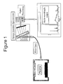
- Figure 1 shows a schematic view of a typical OES configuration.
- the composition of the plasma, and in particular the presence of reactive etch species or etch by-products will determine the spectra (i. e., intensity vs. wavelength) of the emitted radiation.
- the composition of the plasma changes, resulting in a change in the emission spectrum.
- an OES endpoint system By continuously monitoring the plasma emission, it is possible for an OES endpoint system to detect that change and use it to determine when the film has completely cleared. For example, when the OES signal drops below a pre-determined threshold level, this transition is used to trigger "endpoint".
- most of the information relating to endpoint is usually contained within a few wavelengths that correspond to reactants consumed or the etch by-products that are generated during the etch.
- a common method to develop an OES endpoint strategy is to collect a number of spectra of the plasma emission (emission intensity v. wavelength) during both pre-endpoint and post-endpoint conditions.
- Endpoint wavelength candidate-regions can be determined using a number of methods. Spectral regions for endpoint detection can be chosen through statistical methods such as factor analysis or principal component analysis (see U. S. Patent 5,658, 423 to Angell et al . ).
- Another strategy to determine endpoint candidates is through the construction of a difference plot between pre-endpoint (main etch) and post-endpoint (over etch) spectra. Once candidate regions have been selected, assignments of likely chemical species are made for the candidate regions(i. e. , reactant species from dissociated gas precursors or etch products).
- TDM time division multiplexed
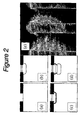
- FIGS 2 (a) to 2 (d) are pictorial examples of one type of the TDM process for deep silicon etching.
- the TDM Si etch process is typically carried out in a reactor configured with a high-density plasma source, typically an Inductively Coupled Plasma (ICP), in conjunction with a radio frequency (RF) biased substrate electrode.
- ICP Inductively Coupled Plasma
- RF radio frequency biased substrate electrode.
- the most common process gases used in the TDM etch process for Si are sulfur hexafluoride (SF 6 ) and octofluorocyclobutane(C 4 F 8 ).
- SF 6 is typically used as the etch gas and C 4 F 8 as the deposition gas.
- SF 6 facilitates spontaneous and isotropic etching of Si ( Figures 2 (a) and 2 (b) )
- C 4 F 8 facilitates protective polymer deposition onto the sidewalls as well as the bottom of etched structures ( Figure 2 (c) ).
- the TDM Si etch process cyclically alternates between etch and deposition process steps enabling high aspect ratio structures to be defined into a masked Si substrate. Upon energetic and directional ion bombardment to the Si substrate, which is present in etch steps, the polymer film coated in the bottom of etched structures from the previous deposition step will be removed to expose the Si surface for further etching ( Figure 2(d) ).
- FIG. 2 (e) shows a scanning electron microscope (SEM) image of a cross section of a silicon structure etched using a TDM process.
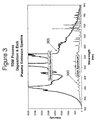
- the plasma emission spectra of etch 300 and deposition 305 steps in a TDM Si etch process are dramatically different due to the different plasma conditions that exist in the deposition and etch steps (e. g., process gas types, pressures, RF powers, etc. ).
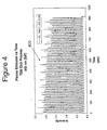
- applying conventional OES methods to a TDM silicon etch process results in an end point trace 400 that is periodic, and cannot be used to detect endpoint.
- the majority of the etch endpoint information is contained within the etch segments of the process.
- U. S. Patent 6,200,822 to Becker et al shows a method to extract endpoint information from the plasma emission of a TDM Si etch process.
- Becker et al. examine the emission intensity of at least one species (typically F or SiF for an Si etch) in the plasma only during the etch step through the use of an externally supplied trigger (typically the transition from one process step to the next).
- an external trigger typically in conjunction with a delay function and a sample-and-hold (peak-hold) circuit, the emission intensity observed in subsequent etch steps can be stitched together to obtain an emission signal that is not periodic in nature.
- the value of the emission intensity for the species in the etch step is held at the last known value during the ensuing deposition step.
- the periodic emission signal is converted into a curve similar to a step function that can be used for process endpoint determination.
- the limitations of this approach are the need for an externally supplied trigger, in addition to the need for a user input delay between the trigger and acquiring the emission data during etch steps.
- U. S. Patent 4,491, 499 to Jerde et al discloses measuring a narrow band of the emission spectrum while simultaneously measuring the intensity of a wider background band centered about the narrow band. In this manner the background signal can be subtracted from the endpoint signal resulting in a more accurate value of the narrow band signal.
- a method of establishing endpoint during a time division multiplex process comprises the steps of subjecting a substrate to the time division multiplex process; monitoring an attribute of a signal generated from the time division multiplex process; processing said attribute of the periodic signal generated from the time division multiplex process using an envelope follower algorithm ; and discontinuing the time division multiplex process at a time based on the processing step.
- a substrate is subjected to the time division multiplex process within a vacuum chamber.
- An attribute, such as emission intensity or plasma impedance, of a periodic signal that is generated by the time division multiplex process is monitored using known optical emission spectrometry techniques.
- the monitoring can be of a plurality of regions of plasma emission intensity.
- the plurality of regions of plasma emission intensity can be chosen using a statistical method such as factor analysis or through an off-line analysis.
- the off-line analysis can be determined by the use of spectra differencing.
- the plurality of regions of plasma emission intensity can be background corrected. Mathematical operations can be performed on multiple regions of plasma emission intensity.
- the attribute of the periodic signal that is generated by the time division multiplex process is processed using an envelope follower algorithm.
- the envelope follower algorithm can use a plurality of peak detect algorithms, can be reset sequentially in a round robin fashion, and can be processed in parallel. Further, the reset can be based a clock period that is at least half the process period of the time division multiplex process. In addition, further processing can be conducted on the extracted amplitude detection signal, including digital signal processing that is filtered using an infinite impulse response filter or a finite impulse response filter. The time division multiplex process is discontinued when endpoint is reached at a time that is based on the processing step.
- TDM time division multiplexed
- the block diagram of Figure 5 shows an overview of the improved OES technique for TDM processes.
- a TDM process is constructed as is well known in the art. At least one region of the plasma emission spectrum (typically within 200-1100 nm for plasma emission) of the TDM process is identified for process endpoint detection. The spectral region (s) is monitored over time during the course of the TDM etch process. The raw emission signal from a TDM process is periodic in nature.
- the envelope follower technique can be used to extract amplitude information from complex waveforms.
- the envelope follower algorithm consists of two or more peak-hold routines operating in parallel that are sequentially reset in a round-robin fashion.
- a second technique consists of a peak-hold algorithm in conjunction with a decay algorithm.
- the peak-hold algorithm is applied to the input data.
- the input data value is compared to the peak-hold value. If the input value is less than the held peak value, the peak value is allowed to decrease over time following a user defined function.
- the decay function can be either linear or non-linear.
- An alternate embodiment of the invention filters the raw data prior to applying the endpoint detection algorithm.
- filtering include, but are not limited to, finite impulse response (FIR) and infinite impulse response (IIR) filters.
- the resulting endpoint trace can be filtered to improve the signal to noise characteristics of the final signal.
- FIR, IIR and other filters may be applied.
- the approach is not limited to a two step cyclical process. In practice it is common to further subdivide the etch portion of the process into a number of sub-steps.
- process parameters within each repetitive loop are not required to remain constant cycle to cycle.
- process morphine it is common during the TDM etching of silicon to gradually decrease the efficiency of the deposition step over the course of the process to maintain profile control (known in the art as process morphine).
- process morphed process small parameter changes are made between some number of etch or deposition steps including, but not limited to, RF bias power, process pressure, ICP power, etc. These changes can also include changing the duration time of the process steps within a TDM cycle.
- a third method to determine a material transition in a TDM process is to filter the data using an FIR, IIR or similar filter without a peak detection algorithm. Contrary to the teachings of Litvak et al. in WO91/18283 the filters do not need to be applied over an integral number of plasma modulation cycles in order to be effective.
- a TDM recipe was used to etch a silicon on insulator (SOI) wafer.
- the recipe is listed in Table 2 below. The example below applies the invention to a 3-step TDM Si etch process.
- the 440 nm peak is assignable to SiF emission (etch product-decreases as the Si is cleared) while the 686 nm peak is assignable to F emission (reactant-increases as the Si is cleared).
- a plot of the value within the 440 nm region versus time shows only a slight decrease in the peak-to-peak values of the oscillating signal as the etch proceeds, and it is difficult to determine a process endpoint.
- FIG. 8 shows a magnified view of the pre-endpoint 800 and post-end point 805 Etch B emission spectra in order to more closely examine the 440 nm peak.
- two spectral regions were monitored,i. e., a narrow 440 nm peak 810 (SiF emission) and a broader spectral region centered around 445 nm 815 for background correction.
- Figure 9 shows a magnified view of the emission intensities at 440 nm and 445 nm over the range of 300 to 400 seconds of total etch time.
- the signal 900 (440 nm) and background 905 (445 nm) regions track each other well (equal or parallel) during the higher intensity deposition step, but diverge near the end of the Etch B step 910.
- Constructing the ratio of the 440 nm signal (designated R1) to the 445 nm background (designated R3) results in the data shown in Figure 10 . Note the periodic and repeating nature of the ratio signal 1000.
- Figure 11 shows the background corrected signal (ratio of 440 nm SiF/445 nm background) over the course of the etch. Note the marked decrease in successive peak heights 1100 near 600 seconds.
- Figure 12 shows a flowchart for the envelope follower TDM endpoint algorithm. Once the data has been acquired, it can be filtered prior to applying the envelope follower.
- Figure 13 shows the data 1300 from Figure 11 after a finite response filter (5 point moving average) has been applied 1305.
- Figures 14 and 15 show the first step of the envelope follower algorithm of the present invention.
- Figure 14 is a graph of a peak-hold algorithm 1400 with reset 1410 applied to the filtered input data 1405 of Figure 13 .
- Figure 15 is a graph of the envelope follower algorithm using multiple peak-holds (1500 and 1505) with sequential resets applied to the filtered input data 1510 of Figure 13 .
- the data for Figures 14 and 15 were acquired at 1 Hz.
- the next step of the envelope follower algorithm determines the maximum value 1600 of the sequential peak hold circuits 1610 (see Figure 16 ).
- Figure 17 shows the resultant envelope follower 1700 for the process. Note the drop in magnitude 1705 near 550 seconds.
- FIG 18 shows the envelope follower signal before 1800 and after 1805 an FIR filter (45 seconds moving average) was applied.
- Figure 19 shows the initial corrected emission input data with the filtered envelope follower endpoint trace 1905.
- the filtered envelope follower trace can subsequently be further processed using commonly known techniques (such as threshold crossing detection or derivative processing) to determine the time at which "endpoint" occurs.
- Figure 20 shows a flowchart for the peak-hold and decay TDM endpoint algorithm.
- Figure 21 shows examples of both linear 2100 and non-linear 2105 decay functions applied to the same input data 2110.
- Figure 22 shows an example of the peak hold 2200 with a linear decay of 55 seconds (e. g., the current peak value would decay to a value of zero in 55 sample intervals).
- the data was acquired at 1 Hz.
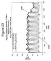
- Figure 23 shows the peak hold with linear decay 2300 applied to the filtered input data 2305.
- a FIR filter was applied after the peak hold decay algorithm.
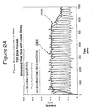
- Figure 24 shows the peak-hold with decay signal before 2400 and after 2405 the FIR filter (30 seconds moving average) was applied.
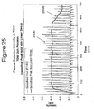
- Figure 25 shows the initial corrected emission input data 2500 with the filtered peak hold decay endpoint trace 2505.
- the filtered peak hold decay trace can subsequently be further processed using commonly known techniques (such as threshold crossing detection or derivative processing) to determine the time at which "endpoint" occurs.
Landscapes
- Engineering & Computer Science (AREA)
- Physics & Mathematics (AREA)
- Plasma & Fusion (AREA)
- Chemical & Material Sciences (AREA)
- Analytical Chemistry (AREA)
- Manufacturing & Machinery (AREA)
- Geometry (AREA)
- Microelectronics & Electronic Packaging (AREA)
- Drying Of Semiconductors (AREA)
- ing And Chemical Polishing (AREA)
- Time-Division Multiplex Systems (AREA)
- Television Systems (AREA)
- Supplying Of Containers To The Packaging Station (AREA)
Abstract
Description
- The present invention generally relates to the field of semiconductor wafer processing. More particularly, the present invention is directed to determining the endpoint of etching processes during a time division multiplexed etching and deposition process.
- During the fabrication of many micro-electro-mechanical (MEMS) devices it is required to etch a layer of material to completion stopping on the layer below (e. g., Silicon on Insulator (SOI) -clearing a silicon (Si) layer stopping on an underlying silicon dioxide (SiO2) layer). Allowing the etch process to proceed beyond the time when the first layer has been removed can result in reduced thickness of the underlying stop layer, or feature profile degradation (known in the art as "notching" for SOI applications).
- As a result, it is crucial in a plasma processing process such as etching that the endpoint of the plasma processing be judged accurately to end the plasma processing with no delay. As a method for detecting the endpoint of plasma processing, a method in which any change in the light spectrum of a specific substance contained within the plasma in the processing chamber is detected, with the endpoint being detected based upon such change, is well known in the art. This method, which is conceived from the observation that the contents in the plasma change as the etching on the substrate progresses, aims to detect a real-time endpoint of the etching process accurately by monitoring a change in the intensity of the light spectrum of a specific substance. This method commonly used to detect plasma process termination times is optical emission spectrometry (OES).
- OES analyzes the light emitted from a plasma source to draw inferences about the chemical and physical state of the plasma process. In semiconductor processing this technique is commonly used to detect material interfaces during plasma etch processes. The OES technique involves monitoring the radiation emitted by the plasma, usually in the ultra violet/visible range (200 nm-1100 nm) portion of the light spectrum.
Figure 1 shows a schematic view of a typical OES configuration. The composition of the plasma, and in particular the presence of reactive etch species or etch by-products, will determine the spectra (i. e., intensity vs. wavelength) of the emitted radiation. During the course of an etch process, and especially at a material transition, the composition of the plasma changes, resulting in a change in the emission spectrum. By continuously monitoring the plasma emission, it is possible for an OES endpoint system to detect that change and use it to determine when the film has completely cleared. For example, when the OES signal drops below a pre-determined threshold level, this transition is used to trigger "endpoint". In practice, most of the information relating to endpoint is usually contained within a few wavelengths that correspond to reactants consumed or the etch by-products that are generated during the etch. - A common method to develop an OES endpoint strategy is to collect a number of spectra of the plasma emission (emission intensity v. wavelength) during both pre-endpoint and post-endpoint conditions. Endpoint wavelength candidate-regions can be determined using a number of methods. Spectral regions for endpoint detection can be chosen through statistical methods such as factor analysis or principal component analysis (see U. S. Patent
5,658, 423 to Angell et al . ). Another strategy to determine endpoint candidates is through the construction of a difference plot between pre-endpoint (main etch) and post-endpoint (over etch) spectra. Once candidate regions have been selected, assignments of likely chemical species are made for the candidate regions(i. e. , reactant species from dissociated gas precursors or etch products). The assignment is not critical in determining success of the strategy, but rather assists in understanding and optimizing the wavelength selection process. A number of references including "Tables of Spectral Lines " by Zaidel et al. and "The Identification of Molecular Spectra by Pearse et al. in conjunction with knowledge of the process chemistry can be used to assign likely species identities for the candidate lines. An example of likely endpoint candidates for a silicon etch process in a sulfur hexafluoride (SF6) plasma would be fluorine (F) lines at 687 nm and 703 nm as well as the silicon fluoride (SiF) emission band at 440 nm. Once these regions have been determined, subsequent parts can be processed using the same OES strategy. - While these OES approaches work well for single step processes or processes with a limited number of discrete etch steps (such as an etch initiation followed by a main etch), it is difficult to apply OES to plasma processes with rapid and periodic plasma perturbations. Examples of such time division multiplexed (TDM) processes are disclosed in U. S. Patent
5,501,893 to Laermer et al . , U. S. Patent4,985, 114 to Okudaira et al . , and U. S. Patent4,795, 529 to Kawasaki et al . Laermer et al. disclose a TDM process for etching high aspect ratio features into Si using an alternating series of etch and deposition steps. -
Figures 2 (a) to 2 (d) are pictorial examples of one type of the TDM process for deep silicon etching. The TDM Si etch process is typically carried out in a reactor configured with a high-density plasma source, typically an Inductively Coupled Plasma (ICP), in conjunction with a radio frequency (RF) biased substrate electrode. The most common process gases used in the TDM etch process for Si are sulfur hexafluoride (SF6) and octofluorocyclobutane(C4F8). SF6 is typically used as the etch gas and C4F8 as the deposition gas. During the etch step, SF6 facilitates spontaneous and isotropic etching of Si (Figures 2 (a) and 2 (b) ) ; in the deposition step, C4F8 facilitates protective polymer deposition onto the sidewalls as well as the bottom of etched structures (Figure 2 (c) ). The TDM Si etch process cyclically alternates between etch and deposition process steps enabling high aspect ratio structures to be defined into a masked Si substrate. Upon energetic and directional ion bombardment to the Si substrate, which is present in etch steps, the polymer film coated in the bottom of etched structures from the previous deposition step will be removed to expose the Si surface for further etching (Figure 2(d) ). The polymer film on the sidewall of the etched structures will remain because it is not subjected to direct ion bombardment, inhibiting lateral etching. Using the TDM Si etch approach allows high aspect ratio features to be defined into Si substrates at high etch rates.Figure 2 (e) shows a scanning electron microscope (SEM) image of a cross section of a silicon structure etched using a TDM process. - As shown in
Figure 3 , the plasma emission spectra ofetch 300 anddeposition 305 steps in a TDM Si etch process are dramatically different due to the different plasma conditions that exist in the deposition and etch steps (e. g., process gas types, pressures, RF powers, etc. ). As shown inFigure 4 , applying conventional OES methods to a TDM silicon etch process results in anend point trace 400 that is periodic, and cannot be used to detect endpoint. For the TDM Si etch, it is expected that the majority of the etch endpoint information is contained within the etch segments of the process. - U. S. Patent
6,200,822 to Becker et al . shows a method to extract endpoint information from the plasma emission of a TDM Si etch process. Becker et al. examine the emission intensity of at least one species (typically F or SiF for an Si etch) in the plasma only during the etch step through the use of an externally supplied trigger (typically the transition from one process step to the next). By using an external trigger in conjunction with a delay function and a sample-and-hold (peak-hold) circuit, the emission intensity observed in subsequent etch steps can be stitched together to obtain an emission signal that is not periodic in nature. The value of the emission intensity for the species in the etch step is held at the last known value during the ensuing deposition step. In this manner the periodic emission signal is converted into a curve similar to a step function that can be used for process endpoint determination. The limitations of this approach are the need for an externally supplied trigger, in addition to the need for a user input delay between the trigger and acquiring the emission data during etch steps. - In an effort to increase the OES method sensitivity U. S. Patent
4,491, 499 to Jerde et al . discloses measuring a narrow band of the emission spectrum while simultaneously measuring the intensity of a wider background band centered about the narrow band. In this manner the background signal can be subtracted from the endpoint signal resulting in a more accurate value of the narrow band signal. - Therefore, there is a need for an endpoint strategy for TDM plasma processes that does not require an external trigger and a user input delay past the trigger to synchronize the plasma emission data collection with the process steps.
- Nothing in the prior art provides the benefits attendant with the present invention.
- Therefore, it is an object of the present invention to provide an improvement which overcomes the inadequacies of the prior art devices and which is a significant contribution to the advancement of the semiconductor processing art.
- The foregoing has outlined some of the pertinent objects of the present invention. These objects should be construed to be merely illustrative of some of the more prominent features and applications of the intended invention. Many other beneficial results can be attained by applying the disclosed invention in a different manner or modifying the invention within the scope of the disclosure.
- According to the present invention, a method of establishing endpoint during a time division multiplex process comprises the steps of subjecting a substrate to the time division multiplex process; monitoring an attribute of a signal generated from the time division multiplex process; processing said attribute of the periodic signal generated from the time division multiplex process using an envelope follower algorithm ; and discontinuing the time division multiplex process at a time based on the processing step.
- A substrate is subjected to the time division multiplex process within a vacuum chamber. An attribute, such as emission intensity or plasma impedance, of a periodic signal that is generated by the time division multiplex process is monitored using known optical emission spectrometry techniques. The monitoring can be of a plurality of regions of plasma emission intensity. The plurality of regions of plasma emission intensity can be chosen using a statistical method such as factor analysis or through an off-line analysis. The off-line analysis can be determined by the use of spectra differencing. In addition, the plurality of regions of plasma emission intensity can be background corrected. Mathematical operations can be performed on multiple regions of plasma emission intensity. The attribute of the periodic signal that is generated by the time division multiplex process is processed using an envelope follower algorithm. The envelope follower algorithm can use a plurality of peak detect algorithms, can be reset sequentially in a round robin fashion, and can be processed in parallel. Further, the reset can be based a clock period that is at least half the process period of the time division multiplex process. In addition, further processing can be conducted on the extracted amplitude detection signal, including digital signal processing that is filtered using an infinite impulse response filter or a finite impulse response filter. The time division multiplex process is discontinued when endpoint is reached at a time that is based on the processing step.
-
-
Figure 1 is a schematic view of a typical optical emission spectroscopy configuration; -
Figure 2 is a pictorial example of one type of the TDM process for deep silicon etching; -
Figure 3 is a graph of the intensity versus wavelength for Deposition and Etch Plasma Emission Spectra for a deep silicon etch process; -
Figure 4 is a graph of the Plasma Emission Intensity versus Time for a typical deep silicon etch process focusing on the emission spectra around the 440 nm peak; -
Figure 5 is a block diagram of the improved OES technique for TDM processes; -
Figure 6 is a graph of the Plasma Emission Intensity versus wavelength for a deep silicon etch process focusing on the emission spectra from the Etch B step before and after the silicon has cleared; -
Figure 7 is a graph of the Difference (Post etch-Pre etch) Plasma Emission Intensity versus wavelength for a deep silicon etch process to determine endpoint candidates; -
Figure 8 is a graph of the Plasma Emission Intensity versus wavelength around the 440 nm region for the etch portion of a deep silicon etch process; -
Figure 9 is a graph of Plasma Emission Intensity versus Time focusing on the Signal (440 nm) and Background (445 nm) for a deep silicon etch process; -
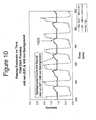
Figure 10 is a graph of Plasma Emission Intensity versus Time focusing on the Signal (440 nm) and Background (445 nm) for a deep silicon etch process and showing the ratio of the 440 nm signal to the 445 nm background; -
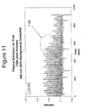
Figure 11 is a graph of the Corrected Plasma Emission Intensity versus Time obtained from the ratio of the 440 nm signal to the 445 nm background over the course of the etch; -
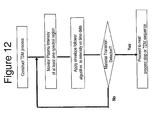
Figure 12 is a flowchart for the envelope follower TDM endpoint algorithm; -
Figure 13 is a graph of the Corrected Plasma Emission Intensity versus Time for a deep silicon etch process using the data fromFigure 11 after a finite response filter has been applied; -
Figure 14 is a graph of Corrected Plasma Emission Intensity versus Time using an envelope follower algorithm with peak-hold and reset applied to the filtered input data ofFigure 13 ; -
Figure 15 is a graph of Corrected Plasma Emission Intensity versus Time using an envelope follower algorithm with multiple peak-holds and sequential resets applied to the filtered input data ofFigure 13 ; -
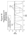
Figure 16 is a graph of Corrected Plasma Emission Intensity versus Time using the envelope follower algorithm to determine the maximum value of the sequential peak hold circuits; -
Figure 17 is a graph of Corrected Plasma Emission Intensity versus Time using the envelope follower of the present invention applied to a TDM etch process; -
Figure 18 is a graph of Corrected Plasma Emission Intensity versus Time using the envelope follower signal before and after an FIR filter was applied; -
Figure 19 is a graph of Corrected Plasma Emission Intensity versus Time showing the initial corrected emission input data with a filtered envelope follower endpoint trace; -
Figure 20 is a flowchart for the peak-hold and decay TDM endpoint algorithm; -
Figure 21 is a graph of Corrected Plasma Emission Intensity versus Time showing examples of both linear and non-linear decay functions applied to the same input data; -
Figure 22 is a graph of Corrected Plasma Emission Intensity versus Time showing an example of the peak hold with a linear decay; -
Figure 23 is a graph of Corrected Plasma Emission Intensity versus Time showing the peak hold with linear decay applied to the filtered input data; -
Figure 24 is a graph of Corrected Plasma Emission Intensity versus Time showing the peak-hold with decay signal before and after the FIR filter was applied; and -
Figure 25 is a graph of Corrected Plasma Emission Intensity versus Time showing the initial corrected emission input data with the filtered peak hold decay endpoint trace. - Similar reference characters refer to similar parts throughout the several views of the drawings.
- We disclose a means of detecting the transition between different materials in a time division multiplexed (TDM) process by analyzing the intensity of at least one wavelength region of the plasma emission without the use of a synchronizing trigger.
- Due to the periodic and repeating nature of a TDM process, by design, the process has a number of characteristic frequencies associated with it. As an example, consider a two step TDM silicon etch process consisting of a five second etch step and a five second deposition step that are subsequently repeated a number of times (see Table 1 below). One characteristic frequency will be 0.1 Hz, determined by the total cycle time (10 seconds).
TABLE 1: Process Parameter Unit of Measure Deposition Etch SF6 Flow sccm 0.5 100 C4F8 Flow sccm 70 0.5 Ar Flow sccm 40 40 Pressure mTorr (1Torr = 133 Pa) 22 23 RF Bias Power W 1 12 ICP Power W 1000 1000 Step Time seconds 5 5 - Note the deposition and etch steps differ in chemistry, RF bias power and pressure resulting in significantly different emission spectra.
- The block diagram of
Figure 5 shows an overview of the improved OES technique for TDM processes. A TDM process is constructed as is well known in the art. At least one region of the plasma emission spectrum (typically within 200-1100 nm for plasma emission) of the TDM process is identified for process endpoint detection. The spectral region (s) is monitored over time during the course of the TDM etch process. The raw emission signal from a TDM process is periodic in nature. - There are a number of ways to detect a material transition in a TDM process without synchronizing the endpoint detection algorithm to the TDM process. These methods include an envelope follower algorithm, and a peak-hold and decay algorithm as well as applying signal processing filters.
- The envelope follower technique can be used to extract amplitude information from complex waveforms. The envelope follower algorithm consists of two or more peak-hold routines operating in parallel that are sequentially reset in a round-robin fashion.
- A second technique consists of a peak-hold algorithm in conjunction with a decay algorithm. The peak-hold algorithm is applied to the input data. The input data value is compared to the peak-hold value. If the input value is less than the held peak value, the peak value is allowed to decrease over time following a user defined function. The decay function can be either linear or non-linear. Once the input value is greater than the decayed hold value, the peak value is updated to the input value, and the decay algorithm restarted. As a result, the algorithm resets itself anytime the input data value exceeds the held value, thereby, avoiding the requirement of synchronizing the algorithm to the TDM process.
- An alternate embodiment of the invention filters the raw data prior to applying the endpoint detection algorithm. Examples of filtering include, but are not limited to, finite impulse response (FIR) and infinite impulse response (IIR) filters.
- Similarly, once the signal has been processed through the endpoint detection algorithm, the resulting endpoint trace can be filtered to improve the signal to noise characteristics of the final signal. Again, FIR, IIR and other filters may be applied.
- Note, the approach is not limited to a two step cyclical process. In practice it is common to further subdivide the etch portion of the process into a number of sub-steps.
- It is also important to note that the process parameters within each repetitive loop are not required to remain constant cycle to cycle. For example, it is common during the TDM etching of silicon to gradually decrease the efficiency of the deposition step over the course of the process to maintain profile control (known in the art as process morphine). In a morphed process, small parameter changes are made between some number of etch or deposition steps including, but not limited to, RF bias power, process pressure, ICP power, etc. These changes can also include changing the duration time of the process steps within a TDM cycle.
- A third method to determine a material transition in a TDM process is to filter the data using an FIR, IIR or similar filter without a peak detection algorithm. Contrary to the teachings of
Litvak et al. in WO91/18283 - While these methods were demonstrated for deep Si etching using an SF6/C4F8 based process, the methods are valid, independent of chemistry, provided a TDM process is utilized. The methods are also useful for detecting material transitions in other materials such as, dielectric materials and metals, where repetitive TDM processes are used.
- A TDM recipe was used to etch a silicon on insulator (SOI) wafer. The recipe is listed in Table 2 below. The example below applies the invention to a 3-step TDM Si etch process.
TABLE 2: Process Parameter Unit of Measure Deposition Etch A Etch B SF6 Flow sccm 1 50 100 C4F8 Flow sccm 70 1 1 Ar Flow sccm 40 40 40 Pressure mTorr (1Torr = 133Pa) 22 23 23 RP Bias Power. W 1 12 12 ICP Power w 1500 1500 1500 Step Time seconds 6 3 7 - The experiments were performed on a commercially available Unaxis Shuttlelock series Deep Silicon Etch (DSE) tool. Emission spectra were collected at a frequency of 1 Hz using a commercially available Unaxis Spectraworks emission spectrometer.
- In order to determine the spectral regions of interest, a test wafer was etched and plasma emission spectra in both the Deposition and Etch B were analyzed prior to and after the silicon layer had been cleared (process endpoint). Since little etching is expected during the deposition phases of the process,
Figure 6 focuses on the emission spectra from the Etch B step before 600 and after 605 the silicon has cleared. Note the slight difference in etch spectra near 450 nm. In order to determine endpoint candidates, a difference spectrum was constructed point-by-point. The resultant spectrum is shown inFigure 7 . Candidates for endpoint detection occur at 440 nm (700) and 686 nm (705). The 440 nm peak is assignable to SiF emission (etch product-decreases as the Si is cleared) while the 686 nm peak is assignable to F emission (reactant-increases as the Si is cleared). As shown previously inFigure 4 , a plot of the value within the 440 nm region versus time shows only a slight decrease in the peak-to-peak values of the oscillating signal as the etch proceeds, and it is difficult to determine a process endpoint. - An improved endpoint strategy was constructed based on the 440 nm emission peak.
Figure 8 shows a magnified view of the pre-endpoint 800 andpost-end point 805 Etch B emission spectra in order to more closely examine the 440 nm peak. In order to reduce correlated noise, two spectral regions were monitored,i. e., a narrow 440 nm peak 810 (SiF emission) and a broader spectral region centered around 445nm 815 for background correction. -
Figure 9 shows a magnified view of the emission intensities at 440 nm and 445 nm over the range of 300 to 400 seconds of total etch time. Note, the signal 900 (440 nm) and background 905 (445 nm) regions track each other well (equal or parallel) during the higher intensity deposition step, but diverge near the end of theEtch B step 910. Constructing the ratio of the 440 nm signal (designated R1) to the 445 nm background (designated R3) results in the data shown inFigure 10 . Note the periodic and repeating nature of theratio signal 1000. -
Figure 11 shows the background corrected signal (ratio of 440 nm SiF/445 nm background) over the course of the etch. Note the marked decrease insuccessive peak heights 1100 near 600 seconds. -
Figure 12 shows a flowchart for the envelope follower TDM endpoint algorithm. Once the data has been acquired, it can be filtered prior to applying the envelope follower.Figure 13 shows thedata 1300 fromFigure 11 after a finite response filter (5 point moving average) has been applied 1305. -
Figures 14 and15 show the first step of the envelope follower algorithm of the present invention.Figure 14 is a graph of a peak-hold algorithm 1400 withreset 1410 applied to the filteredinput data 1405 ofFigure 13 . Whereas,Figure 15 is a graph of the envelope follower algorithm using multiple peak-holds (1500 and 1505) with sequential resets applied to the filteredinput data 1510 ofFigure 13 . The data forFigures 14 and15 were acquired at 1 Hz. - The next step of the envelope follower algorithm determines the
maximum value 1600 of the sequential peak hold circuits 1610 (seeFigure 16 ).Figure 17 shows theresultant envelope follower 1700 for the process. Note the drop inmagnitude 1705 near 550 seconds. - Once the envelope follower has been calculated, additional filtering can be applied to further increase the signal to noise ratio.
Figure 18 shows the envelope follower signal before 1800 and after 1805 an FIR filter (45 seconds moving average) was applied. - In summary,
Figure 19 shows the initial corrected emission input data with the filtered envelopefollower endpoint trace 1905. - The filtered envelope follower trace can subsequently be further processed using commonly known techniques (such as threshold crossing detection or derivative processing) to determine the time at which "endpoint" occurs.
-
Figure 20 shows a flowchart for the peak-hold and decay TDM endpoint algorithm. Once the data has been acquired and filtered (revisitFigure 13 acquired at 1 Hz and filtered with a 5 point moving average) a peak-hold and decay algorithm is applied. -
Figure 21 shows examples of both linear 2100 and non-linear 2105 decay functions applied to thesame input data 2110. -
Figure 22 shows an example of thepeak hold 2200 with a linear decay of 55 seconds (e. g., the current peak value would decay to a value of zero in 55 sample intervals). The data was acquired at 1 Hz. -
Figure 23 shows the peak hold withlinear decay 2300 applied to the filteredinput data 2305. In order to further improve the signal to noise characteristics of the endpoint trace, a FIR filter was applied after the peak hold decay algorithm. -
Figure 24 shows the peak-hold with decay signal before 2400 and after 2405 the FIR filter (30 seconds moving average) was applied. - In summary,
Figure 25 shows the initial correctedemission input data 2500 with the filtered peak holddecay endpoint trace 2505. - The filtered peak hold decay trace can subsequently be further processed using commonly known techniques (such as threshold crossing detection or derivative processing) to determine the time at which "endpoint" occurs.
Claims (19)
- A method of establishing endpoint during a time division multiplex process comprising the steps of:subjecting a substrate to the time division multiplex process;monitoring an attribute of a periodic signal generated from the time division multiplex process;processing said attribute of the periodic signal generated from the time division multiplex process using an envelope follower algorithm; anddiscontinuing the time division multiplex process at a time based on the processing step.
- The method of claim 1 wherein said attribute is plasma emission intensity.
- The method of claim 2 wherein said monitoring step further comprises monitoring a plurality of regions of plasma emission intensity.
- The method of claim 3 wherein said plurality of regions of plasma emission intensity are chosen using a statistical method.
- The method of claim 4 wherein said statistical method further comprises factor analysis.
- The method of claim 3 wherein said plurality of regions of plasma emission intensity are chosen using an off-line analysis.
- The method of claim 6 wherein said off-line analysis further comprises spectra differencing.
- The method of claim 3 wherein said plurality of regions of plasma emission intensity are background corrected.
- The method of claim 3 wherein said monitoring step further comprises performing mathematical operations on said multiple regions of plasma emission intensity.
- The method of claim 1 wherein said attribute is plasma impedance.
- The method of claim 1 wherein said processing step further comprises using a plurality of peak detect algorithms.
- The method of claim 11 wherein said plurality of peak detect algorithms are processed in parallel.
- The method of claim 11 wherein said plurality of peak detect algorithms are reset sequentially in a round robin fashion.
- The method of claim 13 wherein said reset further comprises a clock period that is at least half the process period of the time division multiplex process.
- The method of claim 1 wherein said processing step further comprises post processing of an extracted amplitude detection signal.
- The method of claim 15 wherein said post processing is digital signal processing.
- The method of claim 16 wherein said digital signal processing comprises a filter.
- The method of claim 17 wherein said filter is an infinite impulse response filter.
- The method of claim 17 wherein said filter is a finite impulse response filter.
Applications Claiming Priority (2)
| Application Number | Priority Date | Filing Date | Title |
|---|---|---|---|
| US46933303P | 2003-05-09 | 2003-05-09 | |
| PCT/US2004/014308 WO2004102642A2 (en) | 2003-05-09 | 2004-05-06 | Envelope follower end point detection in time division multiplexed processes |
Publications (2)
| Publication Number | Publication Date |
|---|---|
| EP1623457A2 EP1623457A2 (en) | 2006-02-08 |
| EP1623457B1 true EP1623457B1 (en) | 2008-11-26 |
Family
ID=33452276
Family Applications (1)
| Application Number | Title | Priority Date | Filing Date |
|---|---|---|---|
| EP04751610A Expired - Lifetime EP1623457B1 (en) | 2003-05-09 | 2004-05-06 | Endpoint detection in time division multiplexed processes using an envelope follower algorithm |
Country Status (8)
| Country | Link |
|---|---|
| US (1) | US7101805B2 (en) |
| EP (1) | EP1623457B1 (en) |
| JP (2) | JP2007501532A (en) |
| CN (1) | CN100401491C (en) |
| AT (1) | ATE415702T1 (en) |
| DE (1) | DE602004017983D1 (en) |
| TW (1) | TWI319207B (en) |
| WO (1) | WO2004102642A2 (en) |
Families Citing this family (42)
| Publication number | Priority date | Publication date | Assignee | Title |
|---|---|---|---|---|
| US20060006139A1 (en) * | 2003-05-09 | 2006-01-12 | David Johnson | Selection of wavelengths for end point in a time division multiplexed process |
| WO2006054871A1 (en) * | 2004-11-18 | 2006-05-26 | Semisysco Co., Ltd. | Dry etching apparatuses and methods of forming an electric device using the same |
| FR2880470B1 (en) * | 2004-12-31 | 2007-04-20 | Cit Alcatel | DEVICE AND METHOD FOR CONTROLLING THE ETCH DEPTH DURING PLASMA ALTERNATE ETCHING OF SEMICONDUCTOR SUBSTRATES |
| US7625824B2 (en) * | 2005-06-16 | 2009-12-01 | Oerlikon Usa, Inc. | Process change detection through the use of evolutionary algorithms |
| US7728253B2 (en) * | 2005-06-29 | 2010-06-01 | Northeastern University | Nano-particle trap using a microplasma |
| JP4512533B2 (en) * | 2005-07-27 | 2010-07-28 | 住友精密工業株式会社 | Etching method and etching apparatus |
| WO2007031778A1 (en) * | 2005-09-16 | 2007-03-22 | Aviza Technology Limited | A method of etching a feature in a silicone substrate |
| JP2008010818A (en) * | 2006-06-01 | 2008-01-17 | Sumitomo Electric Ind Ltd | Substrate, substrate inspection method, element, and substrate manufacturing method |
| JP4101280B2 (en) | 2006-07-28 | 2008-06-18 | 住友精密工業株式会社 | Plasma etching method and plasma etching apparatus capable of detecting end point |
| JP5234591B2 (en) * | 2006-07-28 | 2013-07-10 | Sppテクノロジーズ株式会社 | Plasma etching method and plasma etching apparatus capable of detecting end point |
| JP5026326B2 (en) * | 2008-04-04 | 2012-09-12 | 株式会社日立ハイテクノロジーズ | Method and system for determining etching process state |
| US9997325B2 (en) | 2008-07-17 | 2018-06-12 | Verity Instruments, Inc. | Electron beam exciter for use in chemical analysis in processing systems |
| US8538572B2 (en) | 2009-06-30 | 2013-09-17 | Lam Research Corporation | Methods for constructing an optimal endpoint algorithm |
| US8295966B2 (en) | 2009-06-30 | 2012-10-23 | Lam Research Corporation | Methods and apparatus to predict etch rate uniformity for qualification of a plasma chamber |
| US8271121B2 (en) | 2009-06-30 | 2012-09-18 | Lam Research Corporation | Methods and arrangements for in-situ process monitoring and control for plasma processing tools |
| US8983631B2 (en) | 2009-06-30 | 2015-03-17 | Lam Research Corporation | Arrangement for identifying uncontrolled events at the process module level and methods thereof |
| US8473089B2 (en) | 2009-06-30 | 2013-06-25 | Lam Research Corporation | Methods and apparatus for predictive preventive maintenance of processing chambers |
| US8618807B2 (en) | 2009-06-30 | 2013-12-31 | Lam Research Corporation | Arrangement for identifying uncontrolled events at the process module level and methods thereof |
| SG176567A1 (en) * | 2009-06-30 | 2012-01-30 | Lam Res Corp | Arrangement for identifying uncontrolled events at the process module level and methods thereof |
| KR101602449B1 (en) * | 2009-09-14 | 2016-03-15 | 삼성전자주식회사 | Apparatus and method for monitoring chamber status in semiconductor fabrication process |
| JP5223878B2 (en) | 2010-03-30 | 2013-06-26 | 株式会社デンソー | Manufacturing method of semiconductor device |
| US8691702B2 (en) | 2011-03-14 | 2014-04-08 | Plasma-Therm Llc | Method and apparatus for plasma dicing a semi-conductor wafer |
| US8802545B2 (en) | 2011-03-14 | 2014-08-12 | Plasma-Therm Llc | Method and apparatus for plasma dicing a semi-conductor wafer |
| US20130048082A1 (en) * | 2011-08-22 | 2013-02-28 | Mirzafer Abatchev | System, method and apparatus for real time control of rapid alternating processes (rap) |
| JP6002487B2 (en) * | 2012-07-20 | 2016-10-05 | 株式会社日立ハイテクノロジーズ | Analysis method, analysis apparatus, and etching processing system |
| CN103117202B (en) * | 2013-02-19 | 2015-09-09 | 中微半导体设备(上海)有限公司 | The end point determination device and method of plasma-treating technology |
| EP2965349A2 (en) | 2013-03-06 | 2016-01-13 | Plasma-Therm, Llc | Method and apparatus for plasma dicing a semi-conductor wafer |
| JP6239294B2 (en) | 2013-07-18 | 2017-11-29 | 株式会社日立ハイテクノロジーズ | Plasma processing apparatus and method of operating plasma processing apparatus |
| US9209178B2 (en) * | 2013-11-25 | 2015-12-08 | International Business Machines Corporation | finFET isolation by selective cyclic etch |
| CA3000982A1 (en) * | 2014-10-10 | 2016-04-14 | Orthobond, Inc. | Method for detecting and analzying surface films |
| US9640371B2 (en) * | 2014-10-20 | 2017-05-02 | Lam Research Corporation | System and method for detecting a process point in multi-mode pulse processes |
| EP3038132B1 (en) * | 2014-12-22 | 2020-03-11 | IMEC vzw | Method and apparatus for real-time monitoring of plasma etch uniformity |
| US10408763B2 (en) * | 2015-01-30 | 2019-09-10 | Mécanique Analytique Inc. | Systems and methods for testing for a gas leak through a gas flow component |
| JP6356615B2 (en) * | 2015-02-06 | 2018-07-11 | 東芝メモリ株式会社 | Semiconductor manufacturing apparatus and semiconductor manufacturing method |
| JP6549917B2 (en) * | 2015-06-26 | 2019-07-24 | 株式会社日立ハイテクノロジーズ | Plasma processing apparatus and data analysis apparatus therefor |
| US10522429B2 (en) | 2015-11-30 | 2019-12-31 | Taiwan Semiconductor Manufacturing Company, Ltd. | Method of manufacturing semiconductor device |
| JP6479713B2 (en) * | 2016-07-11 | 2019-03-06 | 株式会社Kokusai Electric | Semiconductor device manufacturing method, program, and substrate processing apparatus |
| JP6804694B1 (en) * | 2019-02-08 | 2020-12-23 | 株式会社日立ハイテク | Etching equipment, etching methods and detectors |
| GB201916079D0 (en) | 2019-11-05 | 2019-12-18 | Spts Technologies Ltd | Apparatus and method |
| WO2021130798A1 (en) | 2019-12-23 | 2021-07-01 | 株式会社日立ハイテク | Plasma treatment method and wavelength selecting method used for plasma treatment |
| JP7580046B2 (en) * | 2021-01-19 | 2024-11-11 | パナソニックIpマネジメント株式会社 | Plasma etching method, plasma etching apparatus, and method for manufacturing element chip |
| KR20230029188A (en) | 2021-08-24 | 2023-03-03 | 삼성전자주식회사 | Spectroscopic analysis method, method for fabricating semiconductor device using the same, and substrate process system using the same |
Family Cites Families (41)
| Publication number | Priority date | Publication date | Assignee | Title |
|---|---|---|---|---|
| US4528438A (en) * | 1976-09-16 | 1985-07-09 | Northern Telecom Limited | End point control in plasma etching |
| US4491499A (en) * | 1984-03-29 | 1985-01-01 | At&T Technologies, Inc. | Optical emission end point detector |
| JPS61193505A (en) * | 1985-02-22 | 1986-08-28 | Keio Giken Kogyo Kk | Envelope extracting circuit |
| JPS635529A (en) * | 1986-06-25 | 1988-01-11 | Sharp Corp | Etching end point detector |
| KR900007687B1 (en) * | 1986-10-17 | 1990-10-18 | 가부시기가이샤 히다찌세이사꾸쇼 | Method and device for plasma processing |
| JP2918892B2 (en) * | 1988-10-14 | 1999-07-12 | 株式会社日立製作所 | Plasma etching method |
| US5097430A (en) * | 1990-01-16 | 1992-03-17 | Applied Materials, Inc. | Method and apparatus for displaying process end point signal based on emission concentration within a processing chamber |
| US5208644A (en) | 1990-05-18 | 1993-05-04 | Xinix, Inc. | Interference removal |
| US5160402A (en) * | 1990-05-24 | 1992-11-03 | Applied Materials, Inc. | Multi-channel plasma discharge endpoint detection method |
| US5362356A (en) * | 1990-12-20 | 1994-11-08 | Lsi Logic Corporation | Plasma etching process control |
| JPH05114586A (en) * | 1991-10-22 | 1993-05-07 | Nippon Telegr & Teleph Corp <Ntt> | End point detection device for dry etching |
| DE4241045C1 (en) * | 1992-12-05 | 1994-05-26 | Bosch Gmbh Robert | Process for anisotropic etching of silicon |
| US5308414A (en) | 1992-12-23 | 1994-05-03 | International Business Machines Corporation | Method and apparatus for optical emission end point detection in plasma etching processes |
| TW260857B (en) * | 1993-03-04 | 1995-10-21 | Tokyo Electron Co Ltd | |
| US5980767A (en) * | 1994-02-25 | 1999-11-09 | Tokyo Electron Limited | Method and devices for detecting the end point of plasma process |
| JPH08232087A (en) * | 1994-12-08 | 1996-09-10 | Sumitomo Metal Ind Ltd | Etching end point detection method and etching apparatus |
| US5810963A (en) * | 1995-09-28 | 1998-09-22 | Kabushiki Kaisha Toshiba | Plasma processing apparatus and method |
| US5658423A (en) * | 1995-11-27 | 1997-08-19 | International Business Machines Corporation | Monitoring and controlling plasma processes via optical emission using principal component analysis |
| GB9614160D0 (en) * | 1996-07-05 | 1996-09-04 | Gillette Co | Dry shaving apparatus |
| US6649075B1 (en) * | 1996-07-23 | 2003-11-18 | Applied Materials, Inc. | Method and apparatus for measuring etch uniformity of a semiconductor wafer |
| US5928532A (en) * | 1996-11-11 | 1999-07-27 | Tokyo Electron Limited | Method of detecting end point of plasma processing and apparatus for the same |
| DE19730644C1 (en) * | 1997-07-17 | 1998-11-19 | Bosch Gmbh Robert | Detecting material transition in semiconductor structure |
| US5958258A (en) * | 1997-08-04 | 1999-09-28 | Tokyo Electron Yamanashi Limited | Plasma processing method in semiconductor processing system |
| US6060328A (en) * | 1997-09-05 | 2000-05-09 | Advanced Micro Devices, Inc. | Methods and arrangements for determining an endpoint for an in-situ local interconnect etching process |
| US6153115A (en) * | 1997-10-23 | 2000-11-28 | Massachusetts Institute Of Technology | Monitor of plasma processes with multivariate statistical analysis of plasma emission spectra |
| JPH11176815A (en) * | 1997-12-15 | 1999-07-02 | Ricoh Co Ltd | Dry etching end point determination method and dry etching apparatus |
| JP3563949B2 (en) * | 1997-12-19 | 2004-09-08 | 東京エレクトロン株式会社 | Plasma processing method |
| US6046796A (en) * | 1998-04-22 | 2000-04-04 | Advanced Micro Devices, Inc. | Methodology for improved semiconductor process monitoring using optical emission spectroscopy |
| JP3383236B2 (en) * | 1998-12-01 | 2003-03-04 | 株式会社日立製作所 | Etching end point determining method and etching end point determining apparatus |
| GB9827065D0 (en) * | 1998-12-10 | 1999-02-03 | Orbis Technologies Ltd | A plasma etching control device |
| JP4051470B2 (en) * | 1999-05-18 | 2008-02-27 | 東京エレクトロン株式会社 | End point detection method |
| US6368975B1 (en) * | 1999-07-07 | 2002-04-09 | Applied Materials, Inc. | Method and apparatus for monitoring a process by employing principal component analysis |
| JP2001044171A (en) * | 1999-07-28 | 2001-02-16 | Matsushita Electric Ind Co Ltd | Etching end point detection method and apparatus |
| US6492186B1 (en) * | 1999-08-05 | 2002-12-10 | Eaton Corporation | Method for detecting an endpoint for an oxygen free plasma process |
| US6564114B1 (en) * | 1999-09-08 | 2003-05-13 | Advanced Micro Devices, Inc. | Determining endpoint in etching processes using real-time principal components analysis of optical emission spectra |
| US6582618B1 (en) * | 1999-09-08 | 2003-06-24 | Advanced Micro Devices, Inc. | Method of determining etch endpoint using principal components analysis of optical emission spectra |
| US6451158B1 (en) * | 1999-12-21 | 2002-09-17 | Lam Research Corporation | Apparatus for detecting the endpoint of a photoresist stripping process |
| JP4007748B2 (en) * | 2000-05-12 | 2007-11-14 | 東京応化工業株式会社 | End point detection method of plasma etching process |
| US6358760B1 (en) * | 2000-06-01 | 2002-03-19 | Advanced Micro Devices, Inc. | Method for amorphous silicon local interconnect etch |
| US6903826B2 (en) * | 2001-09-06 | 2005-06-07 | Hitachi, Ltd. | Method and apparatus for determining endpoint of semiconductor element fabricating process |
| KR100426988B1 (en) * | 2001-11-08 | 2004-04-14 | 삼성전자주식회사 | end point detector in semiconductor fabricating equipment and method therefore |
-
2004
- 2004-05-06 WO PCT/US2004/014308 patent/WO2004102642A2/en not_active Ceased
- 2004-05-06 CN CNB2004800125707A patent/CN100401491C/en not_active Expired - Lifetime
- 2004-05-06 US US10/841,818 patent/US7101805B2/en not_active Expired - Lifetime
- 2004-05-06 AT AT04751610T patent/ATE415702T1/en not_active IP Right Cessation
- 2004-05-06 DE DE602004017983T patent/DE602004017983D1/en not_active Expired - Lifetime
- 2004-05-06 EP EP04751610A patent/EP1623457B1/en not_active Expired - Lifetime
- 2004-05-06 JP JP2006532855A patent/JP2007501532A/en active Pending
- 2004-05-07 TW TW093112881A patent/TWI319207B/en not_active IP Right Cessation
-
2010
- 2010-08-13 JP JP2010181312A patent/JP2010251813A/en not_active Abandoned
Also Published As
| Publication number | Publication date |
|---|---|
| EP1623457A2 (en) | 2006-02-08 |
| CN1784778A (en) | 2006-06-07 |
| JP2007501532A (en) | 2007-01-25 |
| WO2004102642A3 (en) | 2005-06-23 |
| CN100401491C (en) | 2008-07-09 |
| ATE415702T1 (en) | 2008-12-15 |
| DE602004017983D1 (en) | 2009-01-08 |
| WO2004102642A2 (en) | 2004-11-25 |
| US20040238489A1 (en) | 2004-12-02 |
| JP2010251813A (en) | 2010-11-04 |
| US7101805B2 (en) | 2006-09-05 |
| TWI319207B (en) | 2010-01-01 |
| TW200511429A (en) | 2005-03-16 |
Similar Documents
| Publication | Publication Date | Title |
|---|---|---|
| US7101805B2 (en) | Envelope follower end point detection in time division multiplexed processes | |
| EP1593141B1 (en) | End point detection in time division multiplexed etch processes | |
| US20060006139A1 (en) | Selection of wavelengths for end point in a time division multiplexed process | |
| US5928532A (en) | Method of detecting end point of plasma processing and apparatus for the same | |
| US5739051A (en) | Method and device for detecting the end point of plasma process | |
| KR102342686B1 (en) | Plasma treatment method | |
| US10665516B2 (en) | Etching method and plasma processing apparatus | |
| US6815362B1 (en) | End point determination of process residues in wafer-less auto clean process using optical emission spectroscopy | |
| KR100454348B1 (en) | An improved method and apparatus for detecting optimal endpoints in plasma etch processes | |
| US20040235303A1 (en) | Endpoint determination of process residues in wafer-less auto clean process using optical emission spectroscopy | |
| JP7201828B2 (en) | Plasma processing apparatus and plasma processing method | |
| US20250283760A1 (en) | Optical emission spectroscopy for advanced process characterization | |
| US10153217B2 (en) | Plasma processing apparatus and plasma processing method | |
| US12362158B2 (en) | Method for OES data collection and endpoint detection | |
| Westerman et al. | Endpoint detection method for time division multiplex etch processes | |
| JP3117355B2 (en) | End point detection method for plasma processing | |
| JP2004253813A (en) | Method and apparatus for detecting end point of plasma processing |
Legal Events
| Date | Code | Title | Description |
|---|---|---|---|
| PUAI | Public reference made under article 153(3) epc to a published international application that has entered the european phase |
Free format text: ORIGINAL CODE: 0009012 |
|
| 17P | Request for examination filed |
Effective date: 20051104 |
|
| AK | Designated contracting states |
Kind code of ref document: A2 Designated state(s): AT BE BG CH CY CZ DE DK EE ES FI FR GB GR HU IE IT LI LU MC NL PL PT RO SE SI SK TR |
|
| AX | Request for extension of the european patent |
Extension state: AL HR LT LV MK |
|
| DAX | Request for extension of the european patent (deleted) | ||
| 17Q | First examination report despatched |
Effective date: 20071002 |
|
| RTI1 | Title (correction) |
Free format text: ENDPOINT DETECTION IN TIME DIVISION MULTIPLEXED PROCESSES USING AN ENVELOPE FOLLOWER ALGORITHM |
|
| GRAP | Despatch of communication of intention to grant a patent |
Free format text: ORIGINAL CODE: EPIDOSNIGR1 |
|
| GRAS | Grant fee paid |
Free format text: ORIGINAL CODE: EPIDOSNIGR3 |
|
| GRAA | (expected) grant |
Free format text: ORIGINAL CODE: 0009210 |
|
| AK | Designated contracting states |
Kind code of ref document: B1 Designated state(s): AT BE BG CH CY CZ DE DK EE ES FI FR GB GR HU IE IT LI LU MC NL PL PT RO SE SI SK TR |
|
| REG | Reference to a national code |
Ref country code: GB Ref legal event code: FG4D |
|
| REG | Reference to a national code |
Ref country code: CH Ref legal event code: EP |
|
| REG | Reference to a national code |
Ref country code: IE Ref legal event code: FG4D |
|
| REF | Corresponds to: |
Ref document number: 602004017983 Country of ref document: DE Date of ref document: 20090108 Kind code of ref document: P |
|
| PG25 | Lapsed in a contracting state [announced via postgrant information from national office to epo] |
Ref country code: ES Free format text: LAPSE BECAUSE OF FAILURE TO SUBMIT A TRANSLATION OF THE DESCRIPTION OR TO PAY THE FEE WITHIN THE PRESCRIBED TIME-LIMIT Effective date: 20090308 Ref country code: AT Free format text: LAPSE BECAUSE OF FAILURE TO SUBMIT A TRANSLATION OF THE DESCRIPTION OR TO PAY THE FEE WITHIN THE PRESCRIBED TIME-LIMIT Effective date: 20081126 |
|
| NLV1 | Nl: lapsed or annulled due to failure to fulfill the requirements of art. 29p and 29m of the patents act | ||
| PG25 | Lapsed in a contracting state [announced via postgrant information from national office to epo] |
Ref country code: NL Free format text: LAPSE BECAUSE OF FAILURE TO SUBMIT A TRANSLATION OF THE DESCRIPTION OR TO PAY THE FEE WITHIN THE PRESCRIBED TIME-LIMIT Effective date: 20081126 Ref country code: FI Free format text: LAPSE BECAUSE OF FAILURE TO SUBMIT A TRANSLATION OF THE DESCRIPTION OR TO PAY THE FEE WITHIN THE PRESCRIBED TIME-LIMIT Effective date: 20081126 Ref country code: PL Free format text: LAPSE BECAUSE OF FAILURE TO SUBMIT A TRANSLATION OF THE DESCRIPTION OR TO PAY THE FEE WITHIN THE PRESCRIBED TIME-LIMIT Effective date: 20081126 Ref country code: SI Free format text: LAPSE BECAUSE OF FAILURE TO SUBMIT A TRANSLATION OF THE DESCRIPTION OR TO PAY THE FEE WITHIN THE PRESCRIBED TIME-LIMIT Effective date: 20081126 |
|
| PG25 | Lapsed in a contracting state [announced via postgrant information from national office to epo] |
Ref country code: BG Free format text: LAPSE BECAUSE OF FAILURE TO SUBMIT A TRANSLATION OF THE DESCRIPTION OR TO PAY THE FEE WITHIN THE PRESCRIBED TIME-LIMIT Effective date: 20090226 Ref country code: RO Free format text: LAPSE BECAUSE OF FAILURE TO SUBMIT A TRANSLATION OF THE DESCRIPTION OR TO PAY THE FEE WITHIN THE PRESCRIBED TIME-LIMIT Effective date: 20081126 Ref country code: DK Free format text: LAPSE BECAUSE OF FAILURE TO SUBMIT A TRANSLATION OF THE DESCRIPTION OR TO PAY THE FEE WITHIN THE PRESCRIBED TIME-LIMIT Effective date: 20081126 Ref country code: EE Free format text: LAPSE BECAUSE OF FAILURE TO SUBMIT A TRANSLATION OF THE DESCRIPTION OR TO PAY THE FEE WITHIN THE PRESCRIBED TIME-LIMIT Effective date: 20081126 Ref country code: BE Free format text: LAPSE BECAUSE OF FAILURE TO SUBMIT A TRANSLATION OF THE DESCRIPTION OR TO PAY THE FEE WITHIN THE PRESCRIBED TIME-LIMIT Effective date: 20081126 |
|
| PG25 | Lapsed in a contracting state [announced via postgrant information from national office to epo] |
Ref country code: PT Free format text: LAPSE BECAUSE OF FAILURE TO SUBMIT A TRANSLATION OF THE DESCRIPTION OR TO PAY THE FEE WITHIN THE PRESCRIBED TIME-LIMIT Effective date: 20090427 Ref country code: SE Free format text: LAPSE BECAUSE OF FAILURE TO SUBMIT A TRANSLATION OF THE DESCRIPTION OR TO PAY THE FEE WITHIN THE PRESCRIBED TIME-LIMIT Effective date: 20090226 Ref country code: CZ Free format text: LAPSE BECAUSE OF FAILURE TO SUBMIT A TRANSLATION OF THE DESCRIPTION OR TO PAY THE FEE WITHIN THE PRESCRIBED TIME-LIMIT Effective date: 20081126 |
|
| PG25 | Lapsed in a contracting state [announced via postgrant information from national office to epo] |
Ref country code: SK Free format text: LAPSE BECAUSE OF FAILURE TO SUBMIT A TRANSLATION OF THE DESCRIPTION OR TO PAY THE FEE WITHIN THE PRESCRIBED TIME-LIMIT Effective date: 20081126 |
|
| PLBE | No opposition filed within time limit |
Free format text: ORIGINAL CODE: 0009261 |
|
| STAA | Information on the status of an ep patent application or granted ep patent |
Free format text: STATUS: NO OPPOSITION FILED WITHIN TIME LIMIT |
|
| 26N | No opposition filed |
Effective date: 20090827 |
|
| PG25 | Lapsed in a contracting state [announced via postgrant information from national office to epo] |
Ref country code: MC Free format text: LAPSE BECAUSE OF NON-PAYMENT OF DUE FEES Effective date: 20090531 |
|
| PG25 | Lapsed in a contracting state [announced via postgrant information from national office to epo] |
Ref country code: IE Free format text: LAPSE BECAUSE OF NON-PAYMENT OF DUE FEES Effective date: 20090506 |
|
| PG25 | Lapsed in a contracting state [announced via postgrant information from national office to epo] |
Ref country code: GR Free format text: LAPSE BECAUSE OF FAILURE TO SUBMIT A TRANSLATION OF THE DESCRIPTION OR TO PAY THE FEE WITHIN THE PRESCRIBED TIME-LIMIT Effective date: 20090227 |
|
| REG | Reference to a national code |
Ref country code: CH Ref legal event code: NV Representative=s name: CABINET ROLAND NITHARDT CONSEILS EN PROPRIETE INDU |
|
| PG25 | Lapsed in a contracting state [announced via postgrant information from national office to epo] |
Ref country code: IT Free format text: LAPSE BECAUSE OF FAILURE TO SUBMIT A TRANSLATION OF THE DESCRIPTION OR TO PAY THE FEE WITHIN THE PRESCRIBED TIME-LIMIT Effective date: 20081126 |
|
| PG25 | Lapsed in a contracting state [announced via postgrant information from national office to epo] |
Ref country code: LU Free format text: LAPSE BECAUSE OF NON-PAYMENT OF DUE FEES Effective date: 20090506 |
|
| PG25 | Lapsed in a contracting state [announced via postgrant information from national office to epo] |
Ref country code: HU Free format text: LAPSE BECAUSE OF FAILURE TO SUBMIT A TRANSLATION OF THE DESCRIPTION OR TO PAY THE FEE WITHIN THE PRESCRIBED TIME-LIMIT Effective date: 20090527 |
|
| PG25 | Lapsed in a contracting state [announced via postgrant information from national office to epo] |
Ref country code: TR Free format text: LAPSE BECAUSE OF FAILURE TO SUBMIT A TRANSLATION OF THE DESCRIPTION OR TO PAY THE FEE WITHIN THE PRESCRIBED TIME-LIMIT Effective date: 20081126 |
|
| PG25 | Lapsed in a contracting state [announced via postgrant information from national office to epo] |
Ref country code: CY Free format text: LAPSE BECAUSE OF FAILURE TO SUBMIT A TRANSLATION OF THE DESCRIPTION OR TO PAY THE FEE WITHIN THE PRESCRIBED TIME-LIMIT Effective date: 20081126 |
|
| REG | Reference to a national code |
Ref country code: FR Ref legal event code: PLFP Year of fee payment: 13 |
|
| REG | Reference to a national code |
Ref country code: FR Ref legal event code: PLFP Year of fee payment: 14 |
|
| REG | Reference to a national code |
Ref country code: FR Ref legal event code: PLFP Year of fee payment: 15 |
|
| P01 | Opt-out of the competence of the unified patent court (upc) registered |
Effective date: 20230524 |
|
| PGFP | Annual fee paid to national office [announced via postgrant information from national office to epo] |
Ref country code: FR Payment date: 20230525 Year of fee payment: 20 Ref country code: DE Payment date: 20230519 Year of fee payment: 20 Ref country code: CH Payment date: 20230602 Year of fee payment: 20 |
|
| PGFP | Annual fee paid to national office [announced via postgrant information from national office to epo] |
Ref country code: GB Payment date: 20230523 Year of fee payment: 20 |
|
| REG | Reference to a national code |
Ref country code: DE Ref legal event code: R071 Ref document number: 602004017983 Country of ref document: DE |
|
| REG | Reference to a national code |
Ref country code: CH Ref legal event code: PL |
|
| REG | Reference to a national code |
Ref country code: GB Ref legal event code: PE20 Expiry date: 20240505 |
|
| PG25 | Lapsed in a contracting state [announced via postgrant information from national office to epo] |
Ref country code: GB Free format text: LAPSE BECAUSE OF EXPIRATION OF PROTECTION Effective date: 20240505 |
|
| PG25 | Lapsed in a contracting state [announced via postgrant information from national office to epo] |
Ref country code: GB Free format text: LAPSE BECAUSE OF EXPIRATION OF PROTECTION Effective date: 20240505 |