EP1619783A2 - Converter with limited voltage rise - Google Patents
Converter with limited voltage rise Download PDFInfo
- Publication number
- EP1619783A2 EP1619783A2 EP05405379A EP05405379A EP1619783A2 EP 1619783 A2 EP1619783 A2 EP 1619783A2 EP 05405379 A EP05405379 A EP 05405379A EP 05405379 A EP05405379 A EP 05405379A EP 1619783 A2 EP1619783 A2 EP 1619783A2
- Authority
- EP
- European Patent Office
- Prior art keywords
- power semiconductor
- semiconductor switch
- limiting network
- increase limiting
- current increase
- Prior art date
- Legal status (The legal status is an assumption and is not a legal conclusion. Google has not performed a legal analysis and makes no representation as to the accuracy of the status listed.)
- Granted
Links
Images

Classifications
-
- H—ELECTRICITY
- H02—GENERATION; CONVERSION OR DISTRIBUTION OF ELECTRIC POWER
- H02M—APPARATUS FOR CONVERSION BETWEEN AC AND AC, BETWEEN AC AND DC, OR BETWEEN DC AND DC, AND FOR USE WITH MAINS OR SIMILAR POWER SUPPLY SYSTEMS; CONVERSION OF DC OR AC INPUT POWER INTO SURGE OUTPUT POWER; CONTROL OR REGULATION THEREOF
- H02M7/00—Conversion of ac power input into dc power output; Conversion of dc power input into ac power output
- H02M7/42—Conversion of dc power input into ac power output without possibility of reversal
- H02M7/44—Conversion of dc power input into ac power output without possibility of reversal by static converters
- H02M7/48—Conversion of dc power input into ac power output without possibility of reversal by static converters using discharge tubes with control electrode or semiconductor devices with control electrode
- H02M7/483—Converters with outputs that each can have more than two voltages levels
-
- H—ELECTRICITY
- H02—GENERATION; CONVERSION OR DISTRIBUTION OF ELECTRIC POWER
- H02M—APPARATUS FOR CONVERSION BETWEEN AC AND AC, BETWEEN AC AND DC, OR BETWEEN DC AND DC, AND FOR USE WITH MAINS OR SIMILAR POWER SUPPLY SYSTEMS; CONVERSION OF DC OR AC INPUT POWER INTO SURGE OUTPUT POWER; CONTROL OR REGULATION THEREOF
- H02M1/00—Details of apparatus for conversion
- H02M1/32—Means for protecting converters other than automatic disconnection
- H02M1/34—Snubber circuits
-
- H—ELECTRICITY
- H02—GENERATION; CONVERSION OR DISTRIBUTION OF ELECTRIC POWER
- H02M—APPARATUS FOR CONVERSION BETWEEN AC AND AC, BETWEEN AC AND DC, OR BETWEEN DC AND DC, AND FOR USE WITH MAINS OR SIMILAR POWER SUPPLY SYSTEMS; CONVERSION OF DC OR AC INPUT POWER INTO SURGE OUTPUT POWER; CONTROL OR REGULATION THEREOF
- H02M7/00—Conversion of ac power input into dc power output; Conversion of dc power input into ac power output
- H02M7/42—Conversion of dc power input into ac power output without possibility of reversal
- H02M7/44—Conversion of dc power input into ac power output without possibility of reversal by static converters
- H02M7/48—Conversion of dc power input into ac power output without possibility of reversal by static converters using discharge tubes with control electrode or semiconductor devices with control electrode
- H02M7/483—Converters with outputs that each can have more than two voltages levels
- H02M7/487—Neutral point clamped inverters
-
- H—ELECTRICITY
- H02—GENERATION; CONVERSION OR DISTRIBUTION OF ELECTRIC POWER
- H02M—APPARATUS FOR CONVERSION BETWEEN AC AND AC, BETWEEN AC AND DC, OR BETWEEN DC AND DC, AND FOR USE WITH MAINS OR SIMILAR POWER SUPPLY SYSTEMS; CONVERSION OF DC OR AC INPUT POWER INTO SURGE OUTPUT POWER; CONTROL OR REGULATION THEREOF
- H02M1/00—Details of apparatus for conversion
- H02M1/32—Means for protecting converters other than automatic disconnection
- H02M1/34—Snubber circuits
- H02M1/348—Passive dissipative snubbers
Definitions
- the invention relates to the field of power electronics. It is based on a converter circuit according to the preamble of claim 1.
- IGCT integrated thyristors with commutated drive electrode
- the converter circuit comprises a DC voltage circuit formed by two series-connected capacitors, wherein the DC voltage circuit has a first main terminal and a second main terminal and a partial terminal formed by the two adjacent and interconnected capacitors.
- the capacitance value of the two capacitors is usually the same chosen big.
- a DC voltage Between the first main terminal and the second main terminal is a DC voltage, between which the first main terminal and the sub-terminal, ie at one capacitor consequently half the DC voltage applied and between the sub-terminal and the second main terminal, that is on the other capacitor also half the DC voltage ,
- the converter circuit has a first current increase limiting network, wherein an inductance and a resistance of the first current increase limiting network is connected to the first main terminal, a capacitance of the first current increase limiting network is connected to the resistor and to the partial terminal, and a diode of the first current increase limiting network is connected to the connection point of the resistor connected to the capacity.
- the converter circuit has a second current increase limiting network, wherein an inductance and a resistance of the second current increase limiting network is connected to the second main terminal, a capacitance of the second current increase limiting network is connected to the resistor and to the partial terminal, and a diode of the second current increase limiting network is connected to the connection point of the resistor connected to the capacity.
- a first, second, third and fourth controllable bidirectional power semiconductor switch and a fifth and sixth non-controllable unidirectional power semiconductor switch is provided, wherein the first, second, third and fourth power semiconductor switches are connected in series and the first power semiconductor switch with the inductance of the first current increase limiting network and the fourth power semiconductor switch is connected to the inductance of the second current increase limiting network.
- the fifth and sixth power semiconductor switches are connected in series, the connection point of the fifth power semiconductor switch to the sixth power semiconductor switch being connected to the sub-terminal, the fifth power semiconductor switch being connected to the connection point of the first power semiconductor switch to the second power semiconductor switch, and the sixth power semiconductor switch being connected to the connection point of the third Power semiconductor switch is connected to the fourth power semiconductor switch.
- first, second, third and fourth controllable bidirectional power semiconductor switches in each case a series circuit of a resistor is connected in parallel with a capacitor, wherein the capacitance has a value of typically 500nF and the resistor has a value typically 1 ohm.
- the respective series connection of the resistor with the capacity with the above-mentioned value-based design serves to achieve a balanced voltage distribution at the associated power semiconductor switch at switching state transitions, ie in the transition from the on state to the off state or from the off state to the on state.
- the object of the invention is therefore to further develop a converter circuit of the type mentioned in such a way that the turn-off losses of power semiconductor switches of the converter circuit can be minimized.
- the converter circuit according to the invention comprises a DC voltage circuit formed by two capacitors connected in series, wherein the DC voltage circuit has a first main terminal and a second main terminal and a partial terminal formed by the two adjacent and interconnected capacitors. Furthermore, a first current increase limiting network is provided, wherein an inductance and a resistance of the first current increase limiting network is connected to the first main terminal, a capacitance of the first current increase limiting network is connected to the resistor and to the partial terminal and a diode of the first current increase limiting network is connected to the connection point of the resistor to the capacitance.
- the inventive converter circuit has a second current increase limiting network, wherein an inductance and a resistance of the second current increase limiting network is connected to the second main terminal, a capacitance of the second current increase limiting network is connected to the resistor and to the partial terminal, and a diode of the second current increase limiting network is connected to the connection point of the second current increase limiting network Resistor connected to capacity.
- a first, second, third and fourth controllable bidirectional power semiconductor switch and a fifth and sixth non-controllable unidirectional power semiconductor switch is provided, wherein the first, second, third and fourth power semiconductor switches are connected in series and the first power semiconductor switch with the inductance of the first current increase limiting network and the fourth power semiconductor switch is connected to the inductance of the second current increase limiting network.
- the fifth and sixth power semiconductor switches are connected in series with the connection point of the fifth power semiconductor switch to the sixth power semiconductor switch connected to the sub-terminal, the fifth power semiconductor switch to the connection point of the first power semiconductor switch to the second power semiconductor switch and the sixth power semiconductor switch to the connection point of the third Power semiconductor switch is connected to the fourth power semiconductor switch.
- a first voltage increase limiting network is connected in parallel to the first power semiconductor switch and connected to the diode of the first current increase limiting network. Furthermore, according to the invention, a second voltage increase limiting network is connected in parallel to the fourth power semiconductor switch and connected to the diode of the second current increase limiting network.
- first and second voltage increase limiting network it is possible by means of the first and second voltage increase limiting network according to the invention to limit the voltage increase during the disconnection of the first, second, third, fourth, fifth and sixth power semiconductor switches, which leads to a significant reduction in the turn-off losses and a significant increase in the maximum turn-off current.
- the respective power semiconductor switch can thereby be largely protected against damage or destruction.
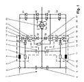
- FIG. 1 shows a first embodiment of the converter circuit according to the invention.
- the converter circuit according to FIG. 1 comprises a DC voltage circuit 1 formed by two capacitors connected in series, the DC voltage circuit 1 having a first main terminal 2 and a second main terminal 3 and a partial terminal 4 formed by the two adjacent and interconnected capacitors.
- an inductor 6 and a resistor 7 of the first current increase limiting network 5 is connected to the first main terminal 2
- a capacitor 8 of the first current increase limiting network 5 with the resistor 7 and to the partial connection 4 and a diode 9 of the first current increase limiting network 5 to the connection point of the resistor 7 is connected to the capacity 8.
- FIG. 1 shows a first embodiment of the converter circuit according to the invention.
- the converter circuit according to FIG. 1 comprises a DC voltage circuit 1 formed by two capacitors connected in series, the DC voltage circuit 1 having a first main terminal 2 and a second main terminal 3 and a partial terminal 4 formed by the two adjacent and interconnected capacitors.
- a second current increase limiting network 10 is provided, an inductance 11 and a resistor 12 of the second current increase limiting network 10 being connected to the second main terminal 3, a capacitor 13 of the second current limiting network 10 being connected to the resistor 12 and to the partial terminal 4 and a diode 14 of the second current increase limiting network 10 is connected to the connection point of the resistor 12 to the capacitor 13.
- the inventive converter circuit has a first, second, third and fourth controllable bidirectional power semiconductor switch S1, S2, S3, S4 and a fifth and sixth non-controllable unidirectional power semiconductor switch S5, S6.
- the fifth and sixth power semiconductor switches S5, S6 is a non-controllable unidirectional power semiconductor switch, each formed by a diode.
- the fifth and sixth power semiconductor switches S5 and S6 form a passive clamp switching group.
- the first, second, third and fourth controllable bidirectional power semiconductor switches S1, S2, S3, S4 are each formed by an integrated thyristor with commutated drive electrode and by a diode connected in anti-parallel to the thyristor.
- the fifth and sixth non-controllable unidirectional power semiconductor switches S5, S6 are preferably each formed by a diode.
- the first, second, third and fourth power semiconductor switches S1, S2, S3, S4 are connected in series and the first power semiconductor switch S1 is connected to the inductor 6 of the first current increase limiting network 5 and the fourth power semiconductor switch S4 is connected to the inductor 11 of the second current increase limiting network 10 connected.
- the fifth and sixth power semiconductor switches S5, S6 are connected in series, the connection point of the fifth power semiconductor switch S5 is connected to the sixth power semiconductor switch S6 to the sub-terminal 4, the fifth power semiconductor switch S6 is connected to the connection point of the first power semiconductor switch S1 to the second power semiconductor switch S2, and sixth power semiconductor switch S6 connected to the connection point of the third power semiconductor switch S3 to the fourth power semiconductor switch S4.
- a first voltage increase limiting network 15 is connected in parallel with the first power semiconductor switch S1 and connected to the diode 9 of the first current increase limiting network 5. Further, a second voltage rise limiting network 16 is parallel to the fourth power semiconductor switch S4 and connected to the diode 14 of the second current increase limiting network 10.
- the second and fourth and sixth power semiconductor switches S2, S4, S6 are switched off, the second voltage increase limiting network 16 causes a current to be driven into the capacitance 20 of the second voltage increase limiting network 16, so that the voltage increases at the second and fourth and sixth power semiconductor switches S2, S4, S6, is limited.
- the limitation of the voltage increase advantageously leads to a significant reduction in the turn-off losses and to a significant increase in the maximum turn-off current to the respective power semiconductor switches S1, S2, S3, S4, S5, S6, whereby they can be largely protected from damage or destruction.
- the first and second voltage increase limiting network 15, 16 are preferably each formed by a series connection of a diode 17, 18, a capacitor 19, 20 and a resistor 21, 22.
- the diode 9 of the first current increase limiting network 5 is connected to the connection point of the diode 17 with the capacitance 19 of the first voltage increase limiting network 15 according to FIG.
- the diode 17 of the first voltage increase limiting network 15 is connected to the connection point of the first power semiconductor switch S1 to the inductance 6 of the first current increase limiting network 5.
- the diode 14 of the second current increase limiting network 10 according to FIG. 1 is connected to the connection point of the diode 18 with the capacitance 20 of the second voltage increase limiting network 16.
- the diode 18 of the second voltage increase limiting network 16 is connected to the connection point of the fourth power semiconductor switch S4 with the inductance 11 of the second current increase limiting network 10.
- the converter circuit according to the invention has a controllable short-circuit element 23, which is connected to the partial connection 4 and to the connection point of the second to the third power semiconductor switch S2, S3.
- the controllable short-circuit element 23 can thus be very easily integrated into the existing network of power semiconductor switches S1, S2, S3, S4, S5, S6 of the converter circuit, so that space can advantageously be saved.
- the controllable short-circuit element 23 is used in a short circuit in one or more of the power semiconductor switch S1, S2, S3, S4, S5, S6 to ensure that caused by the short circuit short circuit current from the capacitors of the DC circuit 1 only very briefly on the or the short-circuited power semiconductor switch S1 , S2, S3, S4, S5, S6 and then via the short-circuit element 23 is directed to the partial connection 4, so that the or the short-circuited power semiconductor switches S1, S2, S3, S4, S5, S6 are not further damaged, loaded or destroyed.
- the triggerable short-circuit element 23 according to FIG.
- a short-circuit current resulting from the short circuit from the phases is not or only with a small amplitude via the power semiconductor switches S1, S2 , S3, S4, S5, S6, in particular via the diodes flowing the power semiconductor switches S1, S2, S3, S4, S5, S6, so that the power semiconductor switches S1, S2, S3, S4, S5, S6 no longer or not at all damaged, be burdened or destroyed.
- Such a short-circuit current or fault current is directed in this case via the short-circuit element 17 to the partial connection 4.
- the short-circuit element 23 is then activated when a short-circuit current is detected by means of a detection device.
- FIG. 2 shows a second embodiment of the converter circuit according to the invention.
- the second embodiment according to FIG. 2 differs from the first embodiment according to FIG. 1 described in detail above in that a controllable short-circuit element is provided which is connected via an inductance 24 to the connection point of the second to the third power semiconductor switch S2, S3 a series circuit of a resistor 25 with a capacitance 26 is connected in parallel to the drivable short-circuit element 23.
- the inductance 24 and series connection of the resistor 25 with the capacitance 26 are optional.
- This triggerable short-circuit element 23 serves in the case of a short circuit at one or more phases of an electrical alternating voltage network connected to the converter circuit.
- the short-circuit element 23 is then activated when a short-circuit current is detected by means of a detection device, wherein the activatable short-circuit element 23 then short-circuits the phases connected to the short-circuit element 23.
- the short-circuit element 23 according to FIG. 1 and FIG. 2 is advantageously formed from two controllable power semiconductors connected in antiparallel with respective pressure contacting, such as, for example, disc thyristors or GTOs.
- the respective controllable power semiconductor switch of the activatable short-circuit element 23 can also be formed by an integrated thyristor with commutated drive electrode or by a triac.
- a balancing resistor 27 is connected in parallel with the series circuit of the fifth and sixth power semiconductor switches S5, S6.
- the Symmetri fürswiderstand 27 is advantageously used, for example, in a shutdown of all power semiconductor switches S1, S2, S3, S4, S5, S6 to achieve a nearly symmetrical voltage distribution across the power semiconductor switch S1, S2, S3, S4, S5, S6 and thus individual power semiconductor switch S1 , S2, S3, S4, S5, S6 to protect against excessive voltages.
Abstract
Description
Die Erfindung bezieht sich auf das Gebiet der Leistungselektronik. Sie geht aus von einer Umrichterschaltung gemäss dem Oberbegriff des Anspruchs 1.The invention relates to the field of power electronics. It is based on a converter circuit according to the preamble of
Leistungshalbleiterschalter, insbesondere integrierte Thyristoren mit kommutierter Ansteuerelektrode (IGCT), werden derzeit vermehrt in der Umrichtertechnik und insbesondere in Umrichterschaltungen zur Schaltung von drei Spannungsniveaus eingesetzt. Eine solche Umrichterschaltung zur Schaltung von drei Spannungsniveaus ist in "Characterization of IGCTs for Series Connected Operation, Conference Record of Annual Meeting of IEEE Industry Applications Society, 2000, October". Darin umfasst die Umrichterschaltung einen durch zwei in Serie geschaltete Kondensatoren gebildeten Gleichspannungskreis, wobei der Gleichspannungskreis einen ersten Hauptanschluss und einen zweiten Hauptanschluss und einen durch die zwei benachbarten und miteinander verbundenen Kondensatoren gebildeten Teilanschluss aufweist. Der Kapazitätswert der beiden Kondensatoren ist üblicherweise gleich gross gewählt. Zwischen dem ersten Hauptanschluss und dem zweiten Hauptanschluss liegt eine Gleichspannung an, wobei zwischen dem ersten Hauptanschluss und dem Teilanschluss, d.h. am einen Kondensator folglich die halbe Gleichspannung anliegt und zwischen dem Teilanschluss und dem zweiten Hauptanschluss, d.h. am anderen Kondensator folglich ebenfalls die halbe Gleichspannung an.Power semiconductor switches, in particular integrated thyristors with commutated drive electrode (IGCT), are currently being used increasingly in converter technology and in particular in converter circuits for switching three voltage levels. Such a converter circuit for switching three voltage levels is described in "Characterization of IGCTs for Series Connected Operation, Conference Record of the Annual Meeting of the IEEE Industry Applications Society, 2000, October". Therein, the converter circuit comprises a DC voltage circuit formed by two series-connected capacitors, wherein the DC voltage circuit has a first main terminal and a second main terminal and a partial terminal formed by the two adjacent and interconnected capacitors. The capacitance value of the two capacitors is usually the same chosen big. Between the first main terminal and the second main terminal is a DC voltage, between which the first main terminal and the sub-terminal, ie at one capacitor consequently half the DC voltage applied and between the sub-terminal and the second main terminal, that is on the other capacitor also half the DC voltage ,
Ferner weist die Umrichterschaltung ein erstes Stromanstiegsbegrenzungsnetzwerk auf, wobei eine Induktivität und ein Widerstand des ersten Stromanstiegsbegrenzungsnetzwerks mit dem ersten Hauptanschluss verbunden ist, eine Kapazität des ersten Stromanstiegsbegrenzungsnetzwerks mit dem Widerstand und mit dem Teilanschluss verbunden ist und eine Diode des ersten Stromanstiegsbegrenzungsnetzwerks mit dem Verbindungspunkt des Widerstands mit der Kapazität verbunden ist. Desweiteren weist die Umrichterschaltung ein zweites Stromanstiegsbegrenzungsnetzwerk auf, wobei eine Induktivität und ein Widerstand des zweiten Stromanstiegsbegrenzungsnetzwerks mit dem zweiten Hauptanschluss verbunden ist, eine Kapazität des zweiten Stromanstiegsbegrenzungsnetzwerks mit dem Widerstand und mit dem Teilanschluss verbunden ist und eine Diode des zweiten Stromanstiegsbegrenzungsnetzwerks mit dem Verbindungspunkt des Widerstands mit der Kapazität verbunden ist. Darüber hinaus ist ein erster, zweiter, dritter und vierter ansteuerbarer bidirektionaler Leistungshalbleiterschalter und ein fünfter und sechster nicht ansteuerbarer unidirektionaler Leistungshalbleiterschalter vorgesehen, wobei der erste, zweite, dritte und vierte Leistungshalbleiterschalter in Serie geschaltet sind und der erste Leistungshalbleiterschalter mit der Induktivität des ersten Stromanstiegsbegrenzungsnetzwerks und der vierte Leistungshalbleiterschalter mit der Induktivität des zweiten Stromanstiegsbegrenzungsnetzwerks verbunden ist. Der fünfte und sechste Leistungshalbleiterschalter ist in Serie geschaltet, wobei der Verbindungspunkt des fünften Leistungshalbleiterschalters mit dem sechsten Leistungshalbleiterschalter mit dem Teilanschluss verbunden ist, der fünfte Leistungshalbleiterschalter mit dem Verbindungspunkt des ersten Leistungshalbleiterschalters mit dem zweiten Leistungshalbleiterschalter verbunden ist und der sechste Leistungshalbleiterschalter mit dem Verbindungspunkt des dritten Leistungshalbleiterschalters mit dem vierten Leistungshalbleiterschalter verbunden ist.Furthermore, the converter circuit has a first current increase limiting network, wherein an inductance and a resistance of the first current increase limiting network is connected to the first main terminal, a capacitance of the first current increase limiting network is connected to the resistor and to the partial terminal, and a diode of the first current increase limiting network is connected to the connection point of the resistor connected to the capacity. Furthermore, the converter circuit has a second current increase limiting network, wherein an inductance and a resistance of the second current increase limiting network is connected to the second main terminal, a capacitance of the second current increase limiting network is connected to the resistor and to the partial terminal, and a diode of the second current increase limiting network is connected to the connection point of the resistor connected to the capacity. In addition, a first, second, third and fourth controllable bidirectional power semiconductor switch and a fifth and sixth non-controllable unidirectional power semiconductor switch is provided, wherein the first, second, third and fourth power semiconductor switches are connected in series and the first power semiconductor switch with the inductance of the first current increase limiting network and the fourth power semiconductor switch is connected to the inductance of the second current increase limiting network. The fifth and sixth power semiconductor switches are connected in series, the connection point of the fifth power semiconductor switch to the sixth power semiconductor switch being connected to the sub-terminal, the fifth power semiconductor switch being connected to the connection point of the first power semiconductor switch to the second power semiconductor switch, and the sixth power semiconductor switch being connected to the connection point of the third Power semiconductor switch is connected to the fourth power semiconductor switch.
Zum ersten, zweiten, dritten und vierten ansteuerbaren bidirektionalen Leistungshalbleiterschalter ist jeweils eine Serienschaltung eines Widerstands mit einer Kapazität parallel geschaltet, wobei die Kapazität einen Wert von typischerweise 500nF und der Widerstand einen Wert typischerweise 1 Ohm aufweist. Die jeweilige Serienschaltung des Widerstands mit der Kapazität mit der vorstehend erwähnten wertemässigen Auslegung dient dazu, eine ausgeglichene Spannungsverteilung an dem zugehörigen Leistungshalbleiterschalter bei Schaltzustandsübergängen, d.h. beim Übergang vom eingeschalteten Zustand zum ausgeschalteten Zustand oder vom ausgeschalteten Zustand zum eingeschalteten Zustand, zu erreichen.For the first, second, third and fourth controllable bidirectional power semiconductor switches in each case a series circuit of a resistor is connected in parallel with a capacitor, wherein the capacitance has a value of typically 500nF and the resistor has a value typically 1 ohm. The respective series connection of the resistor with the capacity with the above-mentioned value-based design serves to achieve a balanced voltage distribution at the associated power semiconductor switch at switching state transitions, ie in the transition from the on state to the off state or from the off state to the on state.
Problematisch bei einer Umrichterschaltung nach "Characterization of IGCTs for Series Connected Operation, Conference Record of Annual Meeting of IEEE Industry Applications Society, 2000, October" ist, dass durch die beschriebene wertemässige Auslegung des Widerstands und der Kapazität der Serienschaltung bei der Abschaltung des zugehörigen Leistungshalbleiterschalters ein hoher Spannungsanstieg bei gleichzeitig hohem Strom auftritt, was zu sehr hohen Abschaltverlusten und dynamischen Überhöhungen der elektrischen Feldstärke im Leistungshalbleiterschalter führt. Solche erhöhten Abschaltverluste und Feldstärken am jeweiligen Leistungshalbleiterschalter können aber diesen beschädigen oder gar zerstören.The problem with a converter circuit according to "Characterization of IGCTs for Series Connected Operation, Conference Record of the Annual Meeting of the IEEE Industry Applications Society, 2000, October" is that the described value-based design of the resistance and the capacity of the series circuit during the disconnection of the associated power semiconductor switch a high voltage rise occurs at the same time as a high current, which leads to very high turn-off losses and dynamic excesses of the electric field strength in the power semiconductor switch. However, such increased turn-off losses and field strengths at the respective power semiconductor switch can damage or even destroy it.
Aufgabe der Erfindung ist es deshalb, eine Umrichterschaltung der eingangs genannten Art derart weiterzuentwickeln, dass die Abschaltverluste an Leistungshalbleiterschaltern der Umrichterschaltung minimiert werden können. Diese Aufgabe wird durch die Merkmale des Anspruchs 1 gelöst. In den abhängigen Ansprüchen sind vorteilhafte Weiterbildungen der Erfindung angegeben.The object of the invention is therefore to further develop a converter circuit of the type mentioned in such a way that the turn-off losses of power semiconductor switches of the converter circuit can be minimized. This object is solved by the features of
Die erfindungsgemässe Umrichterschaltung umfasst einen durch zwei in Serie geschaltete Kondensatoren gebildeten Gleichspannungskreis, wobei der Gleichspannungskreis einen ersten Hauptanschluss und einen zweiten Hauptanschluss und einen durch die zwei benachbarten und miteinander verbundenen Kondensatoren gebildeten Teilanschluss aufweist. Ferner ist ein erstes Stromanstiegsbegrenzungsnetzwerk vorgesehen, wobei eine Induktivität und ein Widerstand des ersten Stromanstiegsbegrenzungsnetzwerks mit dem ersten Hauptanschluss verbunden ist, eine Kapazität des ersten Stromanstiegsbegrenzungsnetzwerks mit dem Widerstand und mit dem Teilanschluss verbunden ist und eine Diode des ersten Stromanstiegsbegrenzungsnetzwerks mit dem Verbindungspunkt des Widerstands mit der Kapazität verbunden ist. Desweiteren weist die erfindungsgemässe Umrichterschaltung ein zweites Stromanstiegsbegrenzungsnetzwerk auf, wobei eine Induktivität und ein Widerstand des zweiten Stromanstiegsbegrenzungsnetzwerks mit dem zweiten Hauptanschluss verbunden ist, eine Kapazität des zweiten Stromanstiegsbegrenzungsnetzwerks mit dem Widerstand und mit dem Teilanschluss verbunden ist und eine Diode des zweiten Stromanstiegsbegrenzungsnetzwerks mit dem Verbindungspunkt des Widerstands mit der Kapazität verbunden ist. Darüber hinaus ist ein erster, zweiter, dritter und vierter ansteuerbarer bidirektionaler Leistungshalbleiterschalter und ein fünfter und sechster nicht ansteuerbarer unidirektionaler Leistungshalbleiterschalter vorgesehen, wobei der erste, zweite, dritte und vierte Leistungshalbleiterschalter in Serie geschaltet sind und der erste Leistungshalbleiterschalter mit der Induktivität des ersten Stromanstiegsbegrenzungsnetzwerks und der vierte Leistungshalbleiterschalter mit der Induktivität des zweiten Stromanstiegsbegrenzungsnetzwerks verbunden ist. Der fünfte und sechste Leistungshalbleiterschalter ist in Serie geschaltet, wobei der Verbindungspunkt des fünften Leistungshalbleiterschalters mit dem sechsten Leistungshalbleiterschalter mit dem Teilanschluss verbunden ist, der fünfte Leistungshalbleiterschalter mit dem Verbindungspunkt des ersten Leistungshalbleiterschalters mit dem zweiten Leistungshalbleiterschalter verbunden ist und der sechste Leistungshalbleiterschalter mit dem Verbindungspunkt des dritten Leistungshalbleiterschalters mit dem vierten Leistungshalbleiterschalter verbunden ist. Erfindungsgemäss ist ein erstes Spannungsanstiegsbegrenzungsnetzwerk parallel zum ersten Leistungshalbleiterschalter geschaltet und mit der Diode des ersten Stromanstiegsbegrenzungsnetzwerks verbunden. Weiterhin ist erfindungsgemäss ein zweites Spannungsanstiegsbegrenzungsnetzwerk parallel zum vierten Leistungshalbleiterschalter geschaltet und mit der Diode des zweiten Stromanstiegsbegrenzungsnetzwerks verbunden.The converter circuit according to the invention comprises a DC voltage circuit formed by two capacitors connected in series, wherein the DC voltage circuit has a first main terminal and a second main terminal and a partial terminal formed by the two adjacent and interconnected capacitors. Furthermore, a first current increase limiting network is provided, wherein an inductance and a resistance of the first current increase limiting network is connected to the first main terminal, a capacitance of the first current increase limiting network is connected to the resistor and to the partial terminal and a diode of the first current increase limiting network is connected to the connection point of the resistor to the capacitance. Furthermore, the inventive converter circuit has a second current increase limiting network, wherein an inductance and a resistance of the second current increase limiting network is connected to the second main terminal, a capacitance of the second current increase limiting network is connected to the resistor and to the partial terminal, and a diode of the second current increase limiting network is connected to the connection point of the second current increase limiting network Resistor connected to capacity. In addition, a first, second, third and fourth controllable bidirectional power semiconductor switch and a fifth and sixth non-controllable unidirectional power semiconductor switch is provided, wherein the first, second, third and fourth power semiconductor switches are connected in series and the first power semiconductor switch with the inductance of the first current increase limiting network and the fourth power semiconductor switch is connected to the inductance of the second current increase limiting network. The fifth and sixth power semiconductor switches are connected in series with the connection point of the fifth power semiconductor switch to the sixth power semiconductor switch connected to the sub-terminal, the fifth power semiconductor switch to the connection point of the first power semiconductor switch to the second power semiconductor switch and the sixth power semiconductor switch to the connection point of the third Power semiconductor switch is connected to the fourth power semiconductor switch. According to the invention, a first voltage increase limiting network is connected in parallel to the first power semiconductor switch and connected to the diode of the first current increase limiting network. Furthermore, according to the invention, a second voltage increase limiting network is connected in parallel to the fourth power semiconductor switch and connected to the diode of the second current increase limiting network.
Vorteilhaft ist es mittels des erfindungsgemässen ersten und zweiten Spannungsanstiegsbegrenzungsnetzwerks möglich, den Spannungsanstieg bei der Abschaltung des ersten, zweiten, dritten, vierten, fünften und sechsten Leistungshalbleiterschalters zu begrenzen, was zu einer signifikanten Verringerung der Abschaltverluste sowie einer signifikanten Erhöhung des maximal abschaltbaren Stromes führt. Der jeweilige Leistungshalbleiterschalter kann dadurch weitestgehend vor einer Beschädigung oder Zerstörung geschützt werden.Advantageously, it is possible by means of the first and second voltage increase limiting network according to the invention to limit the voltage increase during the disconnection of the first, second, third, fourth, fifth and sixth power semiconductor switches, which leads to a significant reduction in the turn-off losses and a significant increase in the maximum turn-off current. The respective power semiconductor switch can thereby be largely protected against damage or destruction.
Diese und weitere Aufgaben, Vorteile und Merkmale der vorliegenden Erfindung werden aus der nachfolgenden detaillierten Beschreibung bevorzugter Ausführungsformen der Erfindung in Verbindung mit der Zeichnung offensichtlich.These and other objects, advantages and features of the present invention will become more apparent from the following detailed description of preferred embodiments of the invention taken in conjunction with the accompanying drawings.
Es zeigen:
- Fig. 1
- eine erste Ausführungsform einer erfindungsgemässen Umrichterschaltung und
- Fig. 2
- eine zweite Ausführungsform der erfindungsgemässen Umrichterschaltung.
- Fig. 1
- a first embodiment of an inventive converter circuit and
- Fig. 2
- A second embodiment of the inventive converter circuit.
Die in der Zeichnung verwendeten Bezugszeichen und deren Bedeutung sind in der Bezugszeichenliste zusammengefasst aufgelistet. Grundsätzlich sind in den Figuren gleiche Teile mit gleichen Bezugszeichen versehen. Die beschriebenen Ausführungsformen stehen beispielhaft für den Erfindungsgegenstand und haben keine beschränkende Wirkung.The reference numerals used in the drawings and their meaning are listed in the list of reference numerals. Basically, the same parts are provided with the same reference numerals in the figures. The described embodiments are exemplary of the subject invention and have no limiting effect.
In Fig. 1 ist eine erste Ausführungsform der erfindungsgemässen Umrichterschaltung gezeigt. Die Umrichterschaltung gemäss Fig. 1 umfasst einen durch zwei in Serie geschaltete Kondensatoren gebildeten Gleichspannungskreis 1, wobei der Gleichspannungskreis 1 einen ersten Hauptanschluss 2 und einen zweiten Hauptanschluss 3 und einen durch die zwei benachbarten und miteinander verbundenen Kondensatoren gebildeten Teilanschluss 4 aufweist. Ferner ist bei der erfindungsgemässen Umrichterschaltung nach Fig. 1 ein erstes Stromanstiegsbegrenzungsnetzwerk 5 vorgesehen, wobei gemäss Fig. 1 eine Induktivität 6 und ein Widerstand 7 des ersten Stromanstiegsbegrenzungsnetzwerks 5 mit dem ersten Hauptanschluss 2 verbunden ist, eine Kapazität 8 des ersten Stromanstiegsbegrenzungsnetzwerks 5 mit dem Widerstand 7 und mit dem Teilanschluss 4 verbunden ist und eine Diode 9 des ersten Stromanstiegsbegrenzungsnetzwerks 5 mit dem Verbindungspunkt des Widerstands 7 mit der Kapazität 8 verbunden ist. Weiterhin ist gemäss Fig. 1 ein zweites Stromanstiegsbegrenzungsnetzwerk 10 vorgesehen, wobei eine Induktivität 11 und ein Widerstand 12 des zweiten Stromanstiegsbegrenzungsnetzwerks 10 mit dem zweiten Hauptanschluss 3 verbunden ist, eine Kapazität 13 des zweiten Stromanstiegsbegrenzungsnetzwerks 10 mit dem Widerstand 12 und mit dem Teilanschluss 4 verbunden ist und eine Diode 14 des zweiten Stromanstiegsbegrenzungsnetzwerks 10 mit dem Verbindungspunkt des Widerstands 12 mit der Kapazität 13 verbunden ist. Darüber hinaus weist die erfindungsgemässe Umrichterschaltung einen ersten, zweiten, dritten und vierten ansteuerbaren bidirektionalen Leistungshalbleiterschalter S1, S2, S3, S4 und einen fünften und sechsten nicht ansteuerbaren unidirektionalen Leistungshalbleiterschalter S5, S6 auf. Der fünfte und sechste Leistungshalbleiterschalter S5, S6 ist ein nicht ansteuerbarer unidirektionaler Leistungshalbleiterschalter, jeweils gebildet durch eine Diode. Somit bildet der fünfte und sechste Leistungshalbleiterschalter S5 und S6 eine passive Klemmschaltgruppe. Vorzugsweise ist der erste, zweite, dritte und vierte ansteuerbare bidirektionale Leistungshalbleiterschalter S1, S2, S3, S4 jeweils durch einen integrierten Thyristor mit kommutierter Ansteuerelektrode und durch eine zu dem Thyristor antiparallel geschaltete Diode gebildet. Ferner ist der fünfte und sechste nicht ansteuerbare unidirektionale Leistungshalbleiterschalter S5, S6 vorzugsweise jeweils durch eine Diode gebildet.FIG. 1 shows a first embodiment of the converter circuit according to the invention. The converter circuit according to FIG. 1 comprises a
Gemäss Fig. 1 sind der erste, zweite, dritte und vierte Leistungshalbleiterschalter S1, S2, S3, S4 in Serie geschaltet und der erste Leistungshalbleiterschalter S1 ist mit der Induktivität 6 des ersten Stromanstiegsbegrenzungsnetzwerks 5 und der vierte Leistungshalbleiterschalter S4 mit der Induktivität 11 des zweiten Stromanstiegsbegrenzungsnetzwerks 10 verbunden. Desweiteren ist der fünfte und sechste Leistungshalbleiterschalter S5, S6 in Serie geschaltet, der Verbindungspunkt des fünften Leistungshalbleiterschalters S5 mit dem sechsten Leistungshalbleiterschalter S6 mit dem Teilanschluss 4 verbunden, der fünfte Leistungshalbleiterschalter S6 mit dem Verbindungspunkt des ersten Leistungshalbleiterschalters S1 mit dem zweiten Leistungshalbleiterschalter S2 verbunden und der sechste Leistungshalbleiterschalter S6 mit dem Verbindungspunkt des dritten Leistungshalbleiterschalters S3 mit dem vierten Leistungshalbleiterschalter S4 verbunden. Erfindungsgemäss ist ein erstes Spannungsanstiegsbegrenzungsnetzwerk 15 parallel zum ersten Leistungshalbleiterschalter S1 geschaltet und mit der Diode 9 des ersten Stromanstiegsbegrenzungsnetzwerks 5 verbunden. Ferner ist ein zweites Spannungsanstiegsbegrenzungsnetzwerk 16 parallel zum vierten Leistungshalbleiterschalter S4 geschaltet und mit der Diode 14 des zweiten Stromanstiegsbegrenzungsnetzwerks 10 verbunden.1, the first, second, third and fourth power semiconductor switches S1, S2, S3, S4 are connected in series and the first power semiconductor switch S1 is connected to the
Das erste Spannungsanstiegsbegrenzungsnetzwerk 15 bewirkt beim Abschaltvorgang des ersten beziehungsweise dritten und fünften Leistungshalbleiterschalters S1, S3, S5, dass ein Strom in die Kapazität 19 des ersten Spannungsanstiegsbegrenzungsnetzwerks 15 getrieben wird, so dass der Spannungsanstieg am ersten beziehungsweise dritten und fünften Leistungshalbleiterschalters S1, S3, S5, begrenzt wird. Zudem bewirkt das zweite Spannungsanstiegsbegrenzungsnetzwerk 16 beim Abschaltvorgang des zweiten beziehungsweise vierten und sechsten Leistungshalbleiterschalters S2, S4, S6, dass ein Strom in die Kapazität 20 des zweiten Spannungsanstiegsbegrenzungsnetzwerks 16 getrieben wird, so dass der Spannungsanstieg am zweiten beziehungsweise vierten und sechsten Leistungshalbleiterschalters S2, S4, S6, begrenzt wird. Die Begrenzung des Spannungsanstiegs führt vorteilhaft zu einer signifikanten Verringerung der Abschaltverluste sowie zu einer signifikanten Erhöhung des maximal abschaltbaren Stromes an den jeweiligen Leistungshalbleiterschaltern S1, S2, S3, S4, S5, S6, wodurch diese weitestgehend vor einer Beschädigung oder Zerstörung geschützt werden können.The first voltage increase limiting
Gemäss Fig. 1 ist das erste und zweite Spannungsanstiegsbegrenzungsnetzwerk 15, 16 vorzugsweise jeweils durch eine Serieschaltung einer Diode 17, 18, einer Kapazität 19, 20 und einem Widerstand 21, 22 gebildet. Die Diode 9 des ersten Stromanstiegsbegrenzungsnetzwerks 5 ist nach Fig. 1 mit dem Verbindungspunkt der Diode 17 mit der Kapazität 19 des ersten Spannungsanstiegsbegrenzungsnetzwerks 15 verbunden. Insbesondere ist die Diode 17 des ersten Spannungsanstiegsbegrenzungsnetzwerks 15 mit dem Verbindungspunkt des ersten Leistungshalbleiterschalters S1 mit der Induktivität 6 des ersten Stromanstiegsbegrenzungsnetzwerks 5 verbunden. Weiterhin ist die Diode 14 des zweiten Stromanstiegsbegrenzungsnetzwerks 10 gemäss Fig. 1 mit dem Verbindungspunkt der Diode 18 mit der Kapazität 20 des zweiten Spannungsanstiegsbegrenzungsnetzwerks 16 verbunden. Insbesondere ist die Diode 18 des zweiten Spannungsanstiegsbegrenzungsnetzwerks 16 mit dem Verbindungspunkt des vierten Leistungshalbleiterschalters S4 mit der Induktivität 11 des zweiten Stromanstiegsbegrenzungsnetzwerks 10 verbunden.According to FIG. 1, the first and second voltage increase limiting
Gemäss Fig. 1 weist die erfindungsgemässe Umrichterschaltung ein ansteuerbares Kurzschlusselement 23 auf, welches mit dem Teilanschluss 4 und mit dem Verbindungspunkt des zweiten mit dem dritten Leistungshalbleiterschalter S2, S3 verbunden ist. Das ansteuerbare Kurzschlusselement 23 lässt sich somit sehr einfach in den bestehenden Verbund der Leistungshalbleiterschalter S1, S2, S3, S4, S5, S6 der Umrichterschaltung integrieren, so dass vorteilhaft Platz gespart werden kann. Das ansteuerbare Kurzschlusselement 23 dient bei einem Kurzschluss in einem oder mehreren der Leistungshalbleiterschalter S1, S2, S3, S4, S5, S6 dazu, dass ein durch den Kurzschluss bedingter Kurzschlussstrom aus den Kondensatoren des Gleichspannungskreises 1 nur sehr kurz über den oder die kurzschlussbehafteten Leistungshalbleiterschalter S1, S2, S3, S4, S5, S6 und dann über das Kurzschlusselement 23 zum Teilanschluss 4 gelenkt wird, damit das oder die kurzschlussbehafteten Leistungshalbleiterschalter S1, S2, S3, S4, S5, S6 nicht weiter beschädigt, belastet oder zerstört werden. Das ansteuerbare Kurzschlusselement 23 gemäss Fig. 1 dient zudem bei einem Kurzschluss an einer oder mehreren Phasen eines an die Umrichterschaltung angeschlossenen elektrischen Wechselspannungsnetzes dazu, dass ein durch den Kurzschluss bedingter Kurzschlussstrom aus den Phasen nicht oder nur mit einer kleinen Amplitude über die Leistungshalbleiterschalter S1, S2, S3, S4, S5, S6, insbesondere über die Dioden der die Leistungshalbleiterschalter S1, S2, S3, S4, S5, S6 fliesst, damit die Leistungshalbleiterschalter S1, S2, S3, S4, S5, S6 nicht weiter oder überhaupt nicht beschädigt, belastet oder zerstört werden. Ein solcher Kurzschlussstrom bzw. Fehlerstrom wird in diesem Fall über das Kurzschlusselement 17 zum Teilanschluss 4 gelenkt. Das Kurzschlusselement 23 wird dann angesteuert, wenn mittels einer Detektionseinrichtung ein Kurzschlussstrom detektiert wird.According to FIG. 1, the converter circuit according to the invention has a controllable short-
In Fig. 2 ist eine zweite Ausführungsform der erfindungsgemässen Umrichterschaltung gezeigt. Die zweite Ausführungsform gemäss Fig. 2 unterscheidet sich von der vorstehend detailliert beschriebenen ersten Ausführungsform gemäss Fig. 1 darin, dass ein ansteuerbares Kurzschlusselement vorgesehen ist, welches über eine Induktivität 24 mit dem Verbindungspunkt des zweiten mit dem dritten Leistungshalbleiterschalter S2, S3 verbunden ist, wobei eine Serienschaltung eines Widerstands 25 mit einer Kapazität 26 parallel zu dem ansteuerbaren Kurzschlusselement 23 geschaltet ist. Die Induktivität 24 und Serienschaltung des Widerstands 25 mit der Kapazität 26 sind optional. Die vorstehend beschriebene Verschaltung der Induktivität 24, des Widerstands 25 und der Kapazität 26 stellt beim Einschalten des Kurzschlusselementes 23 eine Stromanstiegsbegrenzungseinrichtung, d.h. der Stromanstieg beim Einschalten wird begrenzt, sowie beim Abschalten des Kurzschlusselementes 23 eine Spannungsanstiegsbegrenzungseinrichtung, d.h. der Spannungsanstieg beim Abschalten wird begrenzt, dar. Dieses ansteuerbare Kurzschlusselement 23 gemäss Fig. 2 dient bei einem Kurzschluss an einer oder mehreren Phasen eines an die Umrichterschaltung angeschlossenen elektrischen Wechselspannungsnetzes dazu, dass ein durch den Kurzschluss bedingter Kurzschlussstrom aus den Phasen nicht oder nur mit einer kleinen Amplitude über die Leistungshalbleiterschalter S1, S2, S3, S4, S5, S6, insbesondere über die Dioden der die Leistungshalbleiterschalter S1, S2, S3, S4, S5, S6 fliesst, damit die Leistungshalbleiterschalter S1, S2, S3, S4, S5, S6 nicht weiter oder überhaupt nicht beschädigt, belastet oder zerstört werden. Das Kurzschlusselement 23 wird dann angesteuert, wenn mittels einer Detektionseinrichtung ein Kurzschlussstrom detektiert wird, wobei das ansteuerbare Kurzschlusselement 23 dann die jeweils mit dem Kurzschlusselement 23 verbundene Phasen kurzschliesst.FIG. 2 shows a second embodiment of the converter circuit according to the invention. The second embodiment according to FIG. 2 differs from the first embodiment according to FIG. 1 described in detail above in that a controllable short-circuit element is provided which is connected via an
Das Kurzschlusselement 23 nach Fig. 1 und Fig. 2 ist mit Vorteil aus zwei antiparallel geschalteten ansteuerbaren Leistungshalbleitern mit jeweiliger Druckkontaktierung, wie beispielsweise Scheibenthyristoren oder GTOs, gebildet. Der jeweilige ansteuerbare Leistungshalbleiterschalter des ansteuerbaren Kurzschlusselementes 23 kann aber auch durch einen integrierten Thyristor mit kommutierter Ansteuerelektrode oder durch einen Triac gebildet sein.The short-
Gemäss Fig. 1 und Fig. 2 ist parallel zur Serienschaltung des fünften und sechsten Leistungshalbleiterschalters S5, S6 ein Symmetrierungswiderstand 27 geschaltet. Der Symmetrierungswiderstand 27 dient mit Vorteil dazu, beispielsweise bei einem Abschaltvorgang sämtlicher Leistungshalbleiterschalter S1, S2, S3, S4, S5, S6 eine nahezu symmetrische Spannungsverteilung über den Leistungshalbleiterschalter S1, S2, S3, S4, S5, S6 zu erzielen und somit einzelne Leistungshalbleiterschalter S1, S2, S3, S4, S5, S6 vor zu grossen Spannungen zu schützen.According to FIG. 1 and FIG. 2, a balancing
- 11
- GleichspannungskreisDC circuit
- 22
- erster Hauptanschlussfirst main line
- 33
- zweiter Hauptanschlusssecond main connection
- 44
- Teilanschlusspart connection
- 55
- erstes Stromanstiegsbegrenzungsnetzwerkfirst power rise limit network
- 66
- Induktivität des ersten StromanstiegsbegrenzungsnetzwerksInductance of the first current rise limit network
- 77
- Widerstand des ersten StromanstiegsbegrenzungsnetzwerksResistance of the first current rise limit network
- 88th
- Kapazität des ersten StromanstiegsbegrenzungsnetzwerksCapacity of the first river-access-limiting network
- 99
- Diode des ersten StromanstiegsbegrenzungsnetzwerksDiode of the first current rise limit network
- 1010
- zweites Stromanstiegsbegrenzungsnetzwerksecond electricity increase limit network
- 1111
- Induktivität des zweiten StromanstiegsbegrenzungsnetzwerksInductance of the second current rise limit network
- 1212
- Widerstand des zweiten StromanstiegsbegrenzungsnetzwerksResistor of the second current rise limit network
- 1313
- Kapazität des zweiten StromanstiegsbegrenzungsnetzwerksCapacity of the second current increase limiting network
- 1414
- Diode des zweiten StromanstiegsbegrenzungsnetzwerksDiode of the second current rise limit network
- 1515
- erstes Spannungsanstiegsbegrenzungsnetzwerkfirst voltage increase limiting network
- 1616
- zweites Spannungsanstiegsbegrenzungsnetzwerksecond voltage increase limiting network
- 1717
- Diode des ersten SpannungsanstiegsbegrenzungsnetzwerksDiode of the first voltage rise limiting network
- 1818
- Diode des zweiten SpannungsanstiegsbegrenzungsnetzwerksDiode of the second voltage increase limiting network
- 1919
- Kapazität des ersten SpannungsanstiegsbegrenzungsnetzwerksCapacity of the first voltage rise limiting network
- 2020
- Kapazität des zweiten SpannungsanstiegsbegrenzungsnetzwerksCapacity of the second voltage increase limiting network
- 2121
- Widerstand des ersten SpannungsanstiegsbegrenzungsnetzwerksResistance of the first voltage rise limiting network
- 2222
- Widerstand des zweiten SpannungsanstiegsbegrenzungsnetzwerksResistance of the second voltage increase limiting network
- 2323
- KurzschlusselementShort-circuit element
- 2424
- Induktivitätinductance
- 2525
- Widerstandresistance
- 2626
- Kapazitätcapacity
- 2727
- SymmetrierungswiderstandSymmeterisation resistance
- S1S1
- erste Leistungshalbleiterschalterfirst power semiconductor switch
- S2S2
- zweiter Leistungshalbleiterschaltersecond power semiconductor switch
- S3S3
- dritter Leistungshalbleiterschalterthird power semiconductor switch
- S4S4
- vierter Leistungshalbleiterschalterfourth power semiconductor switch
- S5S5
- fünfter Leistungshalbleiterschalterfifth power semiconductor switch
- S6S6
- sechster Leistungshalbleiterschaltersixth power semiconductor switch
Claims (10)
mit einem zweiten Stromanstiegsbegrenzungsnetzwerk (10), wobei eine Induktivität (11) und ein Widerstand (12) des zweiten Stromanstiegsbegrenzungsnetzwerks (10) mit dem zweiten Hauptanschluss (3) verbunden ist, eine Kapazität (13) des zweiten Stromanstiegsbegrenzungsnetzwerks (10) mit dem Widerstand (12) und mit dem Teilanschluss (4) verbunden ist und eine Diode (14) des zweiten Stromanstiegsbegrenzungsnetzwerks (10) mit dem Verbindungspunkt des Widerstands (12) mit der Kapazität (13) verbunden ist,
mit einem ersten, zweiten, dritten und vierten ansteuerbaren bidirektionalen Leistungshalbleiterschalter (S1, S2, S3, S4) und mit einem fünften und sechsten nicht ansteuerbaren unidirektionalen Leistungshalbleiterschalter (S5, S6), wobei der erste, zweite, dritte und vierte Leistungshalbleiterschalter (S1, S2, S3, S4) in Serie geschaltet sind und der erste Leistungshalbleiterschalter (S1) mit der Induktivität (6) des ersten Stromanstiegsbegrenzungsnetzwerks (5) und der vierte Leistungshalbleiterschalter (S4) mit der Induktivität (11) des zweiten Stromanstiegsbegrenzungsnetzwerks (10) verbunden ist, und
wobei der fünfte und sechste Leistungshalbleiterschalter (S5, S6) in Serie geschaltet ist, der Verbindungspunkt des fünften Leistungshalbleiterschalters (S5) mit dem sechsten Leistungshalbleiterschalter (S6) mit dem Teilanschluss (4) verbunden ist, der fünfte Leistungshalbleiterschalter (S6) mit dem Verbindungspunkt des ersten Leistungshalbleiterschalters (S1) mit dem zweiten Leistungshalbleiterschalter (S2) verbunden ist und der sechste Leistungshalbleiterschalter (S6) mit dem Verbindungspunkt des dritten Leistungshalbleiterschalters (S3) mit dem vierten Leistungshalbleiterschalter (S4) verbunden ist, dadurch gekennzeichnet,
dass ein erstes Spannungsanstiegsbegrenzungsnetzwerk (15) parallel zum ersten Leistungshalbleiterschalter (S1) geschaltet ist und mit der Diode (9) des ersten Stromanstiegsbegrenzungsnetzwerks (5) verbunden ist, und
dass ein zweites Spannungsanstiegsbegrenzungsnetzwerk (16) parallel zum vierten Leistungshalbleiterschalter (S4) geschaltet ist und mit der Diode (14) des zweiten Stromanstiegsbegrenzungsnetzwerks (10) verbunden ist.Converter circuit comprising a DC circuit (1) formed by two capacitors connected in series, wherein the DC circuit (1) comprises a first main terminal (2) and a second main terminal (3) and a partial terminal (4) formed by the two adjacent and interconnected capacitors , comprising a first current increase limiting network (5), wherein an inductor (6) and a resistor (7) of the first current increase limiting network (5) is connected to the first main terminal (2), a capacitance (8) of the first current increase limiting network (5) is connected to the first current increase limiting network (5) Resistor (7) and connected to the partial connection (4) and a diode (9) of the first current increase limiting network (5) is connected to the connection point of the resistor (7) to the capacitor (8),
a second current increase limiting network (10), wherein an inductance (11) and a resistance (12) of the second current increase limiting network (10) is connected to the second main terminal (3), a capacitance (13) of the second current increase limiting network (10) having the resistance (12) and is connected to the partial connection (4) and a diode (14) of the second current increase limiting network (10) is connected to the connection point of the resistor (12) to the capacitor (13),
with a first, second, third and fourth controllable bidirectional power semiconductor switch (S1, S2, S3, S4) and with a fifth and sixth non-controllable unidirectional power semiconductor switch (S5, S6), wherein the first, second, third and fourth power semiconductor switch (S1, S2, S3, S4) are connected in series and the first power semiconductor switch (S1) is connected to the inductance (6) of the first current increase limiting network (5) and the fourth power semiconductor switch (S4) is connected to the inductance (11) of the second current increase limiting network (10) , and
wherein the fifth and sixth power semiconductor switches (S5, S6) are connected in series, the connection point of the fifth power semiconductor switch (S5) to the sixth power semiconductor switch (S6) is connected to the sub-terminal (4), the fifth power semiconductor switch (S6) is connected to the connection point of the first power semiconductor switch (S1) is connected to the second power semiconductor switch (S2), and the sixth power semiconductor switch (S6) is connected to the connection point of the third power semiconductor switch (S3) is connected to the fourth power semiconductor switch (S4), characterized
in that a first voltage increase limiting network (15) is connected in parallel with the first power semiconductor switch (S1) and is connected to the diode (9) of the first current increase limiting network (5), and
in that a second voltage increase limiting network (16) is connected in parallel with the fourth power semiconductor switch (S4) and is connected to the diode (14) of the second current increase limiting network (10).
dass die Diode (14) des zweiten Stromanstiegsbegrenzungsnetzwerks (10) mit dem Verbindungspunkt der Diode (18) mit der Kapazität (20) des zweiten Spannungsanstiegsbegrenzungsnetzwerks (16) verbunden ist.A converter circuit according to claim 2, characterized in that the diode (9) of the first current increase limiting network (5) is connected to the connection point of the diode (17) with the capacitance (19) of the first voltage increase limiting network (15), and
in that the diode (14) of the second current increase limiting network (10) is connected to the connection point of the diode (18) with the capacitance (20) of the second voltage increase limiting network (16).
dass eine Serienschaltung eines Widerstands (25) mit einer Kapazität (26) parallel zu dem ansteuerbaren Kurzschlusselement (23) geschaltet ist.Converter circuit according to one of claims 1 to 5, characterized in that a controllable short-circuit element (23) is provided which is connected via an inductor (24) to the connection point of the second with the third power semiconductor switch (S2, S3), and
in that a series circuit of a resistor (25) having a capacitance (26) is connected in parallel with the activatable short-circuit element (23).
Applications Claiming Priority (1)
| Application Number | Priority Date | Filing Date | Title |
|---|---|---|---|
| DE102004034946A DE102004034946A1 (en) | 2004-07-20 | 2004-07-20 | Voltage rise limited converter circuit |
Publications (3)
| Publication Number | Publication Date |
|---|---|
| EP1619783A2 true EP1619783A2 (en) | 2006-01-25 |
| EP1619783A3 EP1619783A3 (en) | 2009-01-28 |
| EP1619783B1 EP1619783B1 (en) | 2010-02-24 |
Family
ID=35058773
Family Applications (1)
| Application Number | Title | Priority Date | Filing Date |
|---|---|---|---|
| EP05405379A Not-in-force EP1619783B1 (en) | 2004-07-20 | 2005-06-13 | Converter with limited voltage rise |
Country Status (5)
| Country | Link |
|---|---|
| EP (1) | EP1619783B1 (en) |
| AT (1) | ATE459126T1 (en) |
| DE (2) | DE102004034946A1 (en) |
| ES (1) | ES2340594T3 (en) |
| PT (1) | PT1619783E (en) |
Cited By (4)
| Publication number | Priority date | Publication date | Assignee | Title |
|---|---|---|---|---|
| CN100571010C (en) * | 2006-11-09 | 2009-12-16 | 天津理工大学 | PWM commutation system and method for work thereof based on IGCT |
| EP2590314A1 (en) * | 2011-11-03 | 2013-05-08 | ABB Technology AG | Inverter system and electronic switching control system with such inverter systems |
| EP2590313A1 (en) * | 2011-11-03 | 2013-05-08 | ABB Technology AG | Inverter system and electronic switching control system with such innverter systems |
| EP2654190B1 (en) | 2012-04-18 | 2022-11-16 | GE Energy Power Conversion GmbH | Method for operating an electric circuit |
Citations (2)
| Publication number | Priority date | Publication date | Assignee | Title |
|---|---|---|---|---|
| EP0321865A2 (en) * | 1987-12-21 | 1989-06-28 | Siemens Aktiengesellschaft | Commutation-discharging, low power loss three-level inverter |
| EP0727870A2 (en) * | 1995-02-14 | 1996-08-21 | Kabushiki Kaisha Toshiba | Power converter |
Family Cites Families (2)
| Publication number | Priority date | Publication date | Assignee | Title |
|---|---|---|---|---|
| US4670828A (en) * | 1986-02-25 | 1987-06-02 | Sundstrand Corporation | Bi-directional switch for neutral point clamped PWM inverter |
| EP1047180A3 (en) * | 1999-04-20 | 2001-04-11 | ABBPATENT GmbH | ARCP three-point power converter or multi-point power converter |
-
2004
- 2004-07-20 DE DE102004034946A patent/DE102004034946A1/en not_active Withdrawn
-
2005
- 2005-06-13 PT PT05405379T patent/PT1619783E/en unknown
- 2005-06-13 EP EP05405379A patent/EP1619783B1/en not_active Not-in-force
- 2005-06-13 DE DE502005009068T patent/DE502005009068D1/en active Active
- 2005-06-13 ES ES05405379T patent/ES2340594T3/en active Active
- 2005-06-13 AT AT05405379T patent/ATE459126T1/en active
Patent Citations (2)
| Publication number | Priority date | Publication date | Assignee | Title |
|---|---|---|---|---|
| EP0321865A2 (en) * | 1987-12-21 | 1989-06-28 | Siemens Aktiengesellschaft | Commutation-discharging, low power loss three-level inverter |
| EP0727870A2 (en) * | 1995-02-14 | 1996-08-21 | Kabushiki Kaisha Toshiba | Power converter |
Non-Patent Citations (1)
| Title |
|---|
| NAGEL A ET AL: "Characterization of IGCTs for series connected operation" 8. Oktober 2000 (2000-10-08), INDUSTRY APPLICATIONS CONFERENCE, 2000. CONFERENCE RECORD OF THE 2000 IEEE 8-12 OCTOBER 2000, PISCATAWAY, NJ, USA,IEEE, PAGE(S) 1923 - 1929 , XP010521374 ISBN: 978-0-7803-6401-1 * das ganze Dokument * * |
Cited By (4)
| Publication number | Priority date | Publication date | Assignee | Title |
|---|---|---|---|---|
| CN100571010C (en) * | 2006-11-09 | 2009-12-16 | 天津理工大学 | PWM commutation system and method for work thereof based on IGCT |
| EP2590314A1 (en) * | 2011-11-03 | 2013-05-08 | ABB Technology AG | Inverter system and electronic switching control system with such inverter systems |
| EP2590313A1 (en) * | 2011-11-03 | 2013-05-08 | ABB Technology AG | Inverter system and electronic switching control system with such innverter systems |
| EP2654190B1 (en) | 2012-04-18 | 2022-11-16 | GE Energy Power Conversion GmbH | Method for operating an electric circuit |
Also Published As
| Publication number | Publication date |
|---|---|
| PT1619783E (en) | 2010-05-27 |
| EP1619783B1 (en) | 2010-02-24 |
| ES2340594T3 (en) | 2010-06-07 |
| ATE459126T1 (en) | 2010-03-15 |
| DE102004034946A1 (en) | 2006-02-16 |
| DE502005009068D1 (en) | 2010-04-08 |
| EP1619783A3 (en) | 2009-01-28 |
Similar Documents
| Publication | Publication Date | Title |
|---|---|---|
| EP2100368B1 (en) | Semiconductor protective elements for controlling short-circuits at the dc end of voltage source converters | |
| DE10005449B4 (en) | Overvoltage protection device for a matrix converter | |
| DE10323220B4 (en) | Short circuit for a partial converter | |
| EP3211784B1 (en) | Double submodule for a modular multilevel converter and modular multilevel converter comprising same | |
| EP3255773B1 (en) | Low loss double submodule for a modular multi-level converter and modular multi-level converter having same | |
| WO2007087732A1 (en) | Switchgear cell and converter circuit for switching a large number of voltage levels | |
| EP3257147A1 (en) | Converter arrangement and method for short-circuit protection thereof | |
| WO2010025758A1 (en) | Device having a converter | |
| EP3556000A1 (en) | Module for modular multi-level inverter comprising a short-circuiter and capacitor current limiting | |
| EP2092622A1 (en) | Rectifier with short circuit current limiting | |
| EP1619783B1 (en) | Converter with limited voltage rise | |
| EP1453192B1 (en) | Inverter circuit with short cicuit protection | |
| EP2625777B1 (en) | Converter circuit | |
| WO2013064310A1 (en) | Inverter circuit and method for operating such an inverter circuit | |
| EP1619785B1 (en) | Converter circuit with voltage rise rate limitation | |
| EP3662572A1 (en) | Submodule for a modular multilevel converter | |
| DE102004034948A1 (en) | Voltage changer, e.g. for switching three voltage levels in a power semiconductor, has capacitors wired in series to form a direct current voltage circuit and networks for limiting current build-up | |
| EP1516420B1 (en) | Circuit arrangement with a voltage link converter | |
| WO2007051321A2 (en) | Voltage changer circuit for switching a multitude of turn-on voltage levels | |
| EP3652849B1 (en) | Coupling between circuits in drive networks | |
| EP2904625B1 (en) | Dc voltage circuit breaker | |
| DE2831495A1 (en) | Overcurrent protection circuit for static inverter - has diode shunting transistor in series with input smoothing capacitor | |
| DE102004034945A1 (en) | Frequency converter for limiting voltage rises has a direct current voltage circuit formed by two capacitors connected in series | |
| DE102004034944A1 (en) | Inverter with current rise limiter has capacitive dc circuit with two current limiting networks and bi-directional power semiconductor switches in parallel with loss limiting circuit | |
| WO2004105225A2 (en) | Converter circuit |
Legal Events
| Date | Code | Title | Description |
|---|---|---|---|
| PUAI | Public reference made under article 153(3) epc to a published international application that has entered the european phase |
Free format text: ORIGINAL CODE: 0009012 |
|
| AK | Designated contracting states |
Kind code of ref document: A2 Designated state(s): AT BE BG CH CY CZ DE DK EE ES FI FR GB GR HU IE IS IT LI LT LU MC NL PL PT RO SE SI SK TR |
|
| AX | Request for extension of the european patent |
Extension state: AL BA HR LV MK YU |
|
| PUAL | Search report despatched |
Free format text: ORIGINAL CODE: 0009013 |
|
| AK | Designated contracting states |
Kind code of ref document: A3 Designated state(s): AT BE BG CH CY CZ DE DK EE ES FI FR GB GR HU IE IS IT LI LT LU MC NL PL PT RO SE SI SK TR |
|
| AX | Request for extension of the european patent |
Extension state: AL BA HR LV MK YU |
|
| 17P | Request for examination filed |
Effective date: 20090122 |
|
| 17Q | First examination report despatched |
Effective date: 20090323 |
|
| AKX | Designation fees paid |
Designated state(s): AT BE BG CH CY CZ DE DK EE ES FI FR GB GR HU IE IS IT LI LT LU MC NL PL PT RO SE SI SK TR |
|
| GRAP | Despatch of communication of intention to grant a patent |
Free format text: ORIGINAL CODE: EPIDOSNIGR1 |
|
| GRAS | Grant fee paid |
Free format text: ORIGINAL CODE: EPIDOSNIGR3 |
|
| GRAA | (expected) grant |
Free format text: ORIGINAL CODE: 0009210 |
|
| AK | Designated contracting states |
Kind code of ref document: B1 Designated state(s): AT BE BG CH CY CZ DE DK EE ES FI FR GB GR HU IE IS IT LI LT LU MC NL PL PT RO SE SI SK TR |
|
| REG | Reference to a national code |
Ref country code: GB Ref legal event code: FG4D Free format text: NOT ENGLISH |
|
| REG | Reference to a national code |
Ref country code: CH Ref legal event code: EP |
|
| REG | Reference to a national code |
Ref country code: IE Ref legal event code: FG4D Free format text: LANGUAGE OF EP DOCUMENT: GERMAN |
|
| REF | Corresponds to: |
Ref document number: 502005009068 Country of ref document: DE Date of ref document: 20100408 Kind code of ref document: P |
|
| REG | Reference to a national code |
Ref country code: PT Ref legal event code: SC4A Free format text: AVAILABILITY OF NATIONAL TRANSLATION Effective date: 20100520 |
|
| REG | Reference to a national code |
Ref country code: ES Ref legal event code: FG2A Ref document number: 2340594 Country of ref document: ES Kind code of ref document: T3 |
|
| REG | Reference to a national code |
Ref country code: NL Ref legal event code: VDEP Effective date: 20100224 |
|
| LTIE | Lt: invalidation of european patent or patent extension |
Effective date: 20100224 |
|
| PG25 | Lapsed in a contracting state [announced via postgrant information from national office to epo] |
Ref country code: IS Free format text: LAPSE BECAUSE OF FAILURE TO SUBMIT A TRANSLATION OF THE DESCRIPTION OR TO PAY THE FEE WITHIN THE PRESCRIBED TIME-LIMIT Effective date: 20100624 Ref country code: LT Free format text: LAPSE BECAUSE OF FAILURE TO SUBMIT A TRANSLATION OF THE DESCRIPTION OR TO PAY THE FEE WITHIN THE PRESCRIBED TIME-LIMIT Effective date: 20100224 |
|
| PG25 | Lapsed in a contracting state [announced via postgrant information from national office to epo] |
Ref country code: PL Free format text: LAPSE BECAUSE OF FAILURE TO SUBMIT A TRANSLATION OF THE DESCRIPTION OR TO PAY THE FEE WITHIN THE PRESCRIBED TIME-LIMIT Effective date: 20100224 Ref country code: FI Free format text: LAPSE BECAUSE OF FAILURE TO SUBMIT A TRANSLATION OF THE DESCRIPTION OR TO PAY THE FEE WITHIN THE PRESCRIBED TIME-LIMIT Effective date: 20100224 Ref country code: SI Free format text: LAPSE BECAUSE OF FAILURE TO SUBMIT A TRANSLATION OF THE DESCRIPTION OR TO PAY THE FEE WITHIN THE PRESCRIBED TIME-LIMIT Effective date: 20100224 |
|
| REG | Reference to a national code |
Ref country code: IE Ref legal event code: FD4D |
|
| PG25 | Lapsed in a contracting state [announced via postgrant information from national office to epo] |
Ref country code: IE Free format text: LAPSE BECAUSE OF FAILURE TO SUBMIT A TRANSLATION OF THE DESCRIPTION OR TO PAY THE FEE WITHIN THE PRESCRIBED TIME-LIMIT Effective date: 20100224 Ref country code: GR Free format text: LAPSE BECAUSE OF FAILURE TO SUBMIT A TRANSLATION OF THE DESCRIPTION OR TO PAY THE FEE WITHIN THE PRESCRIBED TIME-LIMIT Effective date: 20100525 Ref country code: EE Free format text: LAPSE BECAUSE OF FAILURE TO SUBMIT A TRANSLATION OF THE DESCRIPTION OR TO PAY THE FEE WITHIN THE PRESCRIBED TIME-LIMIT Effective date: 20100224 Ref country code: CY Free format text: LAPSE BECAUSE OF FAILURE TO SUBMIT A TRANSLATION OF THE DESCRIPTION OR TO PAY THE FEE WITHIN THE PRESCRIBED TIME-LIMIT Effective date: 20100224 Ref country code: RO Free format text: LAPSE BECAUSE OF FAILURE TO SUBMIT A TRANSLATION OF THE DESCRIPTION OR TO PAY THE FEE WITHIN THE PRESCRIBED TIME-LIMIT Effective date: 20100224 Ref country code: SE Free format text: LAPSE BECAUSE OF FAILURE TO SUBMIT A TRANSLATION OF THE DESCRIPTION OR TO PAY THE FEE WITHIN THE PRESCRIBED TIME-LIMIT Effective date: 20100224 Ref country code: NL Free format text: LAPSE BECAUSE OF FAILURE TO SUBMIT A TRANSLATION OF THE DESCRIPTION OR TO PAY THE FEE WITHIN THE PRESCRIBED TIME-LIMIT Effective date: 20100224 |
|
| PG25 | Lapsed in a contracting state [announced via postgrant information from national office to epo] |
Ref country code: BG Free format text: LAPSE BECAUSE OF FAILURE TO SUBMIT A TRANSLATION OF THE DESCRIPTION OR TO PAY THE FEE WITHIN THE PRESCRIBED TIME-LIMIT Effective date: 20100524 Ref country code: CZ Free format text: LAPSE BECAUSE OF FAILURE TO SUBMIT A TRANSLATION OF THE DESCRIPTION OR TO PAY THE FEE WITHIN THE PRESCRIBED TIME-LIMIT Effective date: 20100224 Ref country code: SK Free format text: LAPSE BECAUSE OF FAILURE TO SUBMIT A TRANSLATION OF THE DESCRIPTION OR TO PAY THE FEE WITHIN THE PRESCRIBED TIME-LIMIT Effective date: 20100224 |
|
| BERE | Be: lapsed |
Owner name: ABB SCHWEIZ A.G. Effective date: 20100630 |
|
| PLBE | No opposition filed within time limit |
Free format text: ORIGINAL CODE: 0009261 |
|
| STAA | Information on the status of an ep patent application or granted ep patent |
Free format text: STATUS: NO OPPOSITION FILED WITHIN TIME LIMIT |
|
| PG25 | Lapsed in a contracting state [announced via postgrant information from national office to epo] |
Ref country code: MC Free format text: LAPSE BECAUSE OF NON-PAYMENT OF DUE FEES Effective date: 20100630 Ref country code: DK Free format text: LAPSE BECAUSE OF FAILURE TO SUBMIT A TRANSLATION OF THE DESCRIPTION OR TO PAY THE FEE WITHIN THE PRESCRIBED TIME-LIMIT Effective date: 20100224 |
|
| 26N | No opposition filed |
Effective date: 20101125 |
|
| PG25 | Lapsed in a contracting state [announced via postgrant information from national office to epo] |
Ref country code: IT Free format text: LAPSE BECAUSE OF FAILURE TO SUBMIT A TRANSLATION OF THE DESCRIPTION OR TO PAY THE FEE WITHIN THE PRESCRIBED TIME-LIMIT Effective date: 20100224 |
|
| PG25 | Lapsed in a contracting state [announced via postgrant information from national office to epo] |
Ref country code: BE Free format text: LAPSE BECAUSE OF NON-PAYMENT OF DUE FEES Effective date: 20100630 |
|
| PG25 | Lapsed in a contracting state [announced via postgrant information from national office to epo] |
Ref country code: LU Free format text: LAPSE BECAUSE OF NON-PAYMENT OF DUE FEES Effective date: 20100613 Ref country code: HU Free format text: LAPSE BECAUSE OF FAILURE TO SUBMIT A TRANSLATION OF THE DESCRIPTION OR TO PAY THE FEE WITHIN THE PRESCRIBED TIME-LIMIT Effective date: 20100825 |
|
| PG25 | Lapsed in a contracting state [announced via postgrant information from national office to epo] |
Ref country code: TR Free format text: LAPSE BECAUSE OF FAILURE TO SUBMIT A TRANSLATION OF THE DESCRIPTION OR TO PAY THE FEE WITHIN THE PRESCRIBED TIME-LIMIT Effective date: 20100224 |
|
| PGFP | Annual fee paid to national office [announced via postgrant information from national office to epo] |
Ref country code: GB Payment date: 20140618 Year of fee payment: 10 |
|
| PGFP | Annual fee paid to national office [announced via postgrant information from national office to epo] |
Ref country code: DE Payment date: 20140619 Year of fee payment: 10 Ref country code: ES Payment date: 20140627 Year of fee payment: 10 Ref country code: PT Payment date: 20140603 Year of fee payment: 10 Ref country code: AT Payment date: 20140611 Year of fee payment: 10 Ref country code: CH Payment date: 20140618 Year of fee payment: 10 |
|
| PGFP | Annual fee paid to national office [announced via postgrant information from national office to epo] |
Ref country code: FR Payment date: 20140619 Year of fee payment: 10 |
|
| REG | Reference to a national code |
Ref country code: PT Ref legal event code: MM4A Free format text: LAPSE DUE TO NON-PAYMENT OF FEES Effective date: 20151214 |
|
| REG | Reference to a national code |
Ref country code: DE Ref legal event code: R119 Ref document number: 502005009068 Country of ref document: DE |
|
| REG | Reference to a national code |
Ref country code: CH Ref legal event code: PL |
|
| REG | Reference to a national code |
Ref country code: AT Ref legal event code: MM01 Ref document number: 459126 Country of ref document: AT Kind code of ref document: T Effective date: 20150613 |
|
| GBPC | Gb: european patent ceased through non-payment of renewal fee |
Effective date: 20150613 |
|
| PG25 | Lapsed in a contracting state [announced via postgrant information from national office to epo] |
Ref country code: PT Free format text: LAPSE BECAUSE OF NON-PAYMENT OF DUE FEES Effective date: 20151214 |
|
| REG | Reference to a national code |
Ref country code: FR Ref legal event code: ST Effective date: 20160229 |
|
| PG25 | Lapsed in a contracting state [announced via postgrant information from national office to epo] |
Ref country code: DE Free format text: LAPSE BECAUSE OF NON-PAYMENT OF DUE FEES Effective date: 20160101 Ref country code: LI Free format text: LAPSE BECAUSE OF NON-PAYMENT OF DUE FEES Effective date: 20150630 Ref country code: GB Free format text: LAPSE BECAUSE OF NON-PAYMENT OF DUE FEES Effective date: 20150613 Ref country code: CH Free format text: LAPSE BECAUSE OF NON-PAYMENT OF DUE FEES Effective date: 20150630 |
|
| PG25 | Lapsed in a contracting state [announced via postgrant information from national office to epo] |
Ref country code: FR Free format text: LAPSE BECAUSE OF NON-PAYMENT OF DUE FEES Effective date: 20150630 Ref country code: AT Free format text: LAPSE BECAUSE OF NON-PAYMENT OF DUE FEES Effective date: 20150613 |
|
| REG | Reference to a national code |
Ref country code: ES Ref legal event code: FD2A Effective date: 20160728 |
|
| PG25 | Lapsed in a contracting state [announced via postgrant information from national office to epo] |
Ref country code: ES Free format text: LAPSE BECAUSE OF NON-PAYMENT OF DUE FEES Effective date: 20150614 |