EP1619495A1 - Method and Apparatus for inspecting a specimen surface and use of fluorescent materials - Google Patents
Method and Apparatus for inspecting a specimen surface and use of fluorescent materials Download PDFInfo
- Publication number
- EP1619495A1 EP1619495A1 EP04077130A EP04077130A EP1619495A1 EP 1619495 A1 EP1619495 A1 EP 1619495A1 EP 04077130 A EP04077130 A EP 04077130A EP 04077130 A EP04077130 A EP 04077130A EP 1619495 A1 EP1619495 A1 EP 1619495A1
- Authority
- EP
- European Patent Office
- Prior art keywords
- beams
- specimen surface
- primary
- primary beams
- converting
- Prior art date
- Legal status (The legal status is an assumption and is not a legal conclusion. Google has not performed a legal analysis and makes no representation as to the accuracy of the status listed.)
- Withdrawn
Links
Images


Classifications
-
- H—ELECTRICITY
- H01—ELECTRIC ELEMENTS
- H01J—ELECTRIC DISCHARGE TUBES OR DISCHARGE LAMPS
- H01J37/00—Discharge tubes with provision for introducing objects or material to be exposed to the discharge, e.g. for the purpose of examination or processing thereof
- H01J37/02—Details
- H01J37/244—Detectors; Associated components or circuits therefor
-
- G—PHYSICS
- G01—MEASURING; TESTING
- G01N—INVESTIGATING OR ANALYSING MATERIALS BY DETERMINING THEIR CHEMICAL OR PHYSICAL PROPERTIES
- G01N23/00—Investigating or analysing materials by the use of wave or particle radiation, e.g. X-rays or neutrons, not covered by groups G01N3/00 – G01N17/00, G01N21/00 or G01N22/00
- G01N23/22—Investigating or analysing materials by the use of wave or particle radiation, e.g. X-rays or neutrons, not covered by groups G01N3/00 – G01N17/00, G01N21/00 or G01N22/00 by measuring secondary emission from the material
- G01N23/225—Investigating or analysing materials by the use of wave or particle radiation, e.g. X-rays or neutrons, not covered by groups G01N3/00 – G01N17/00, G01N21/00 or G01N22/00 by measuring secondary emission from the material using electron or ion
-
- G—PHYSICS
- G01—MEASURING; TESTING
- G01N—INVESTIGATING OR ANALYSING MATERIALS BY DETERMINING THEIR CHEMICAL OR PHYSICAL PROPERTIES
- G01N23/00—Investigating or analysing materials by the use of wave or particle radiation, e.g. X-rays or neutrons, not covered by groups G01N3/00 – G01N17/00, G01N21/00 or G01N22/00
- G01N23/22—Investigating or analysing materials by the use of wave or particle radiation, e.g. X-rays or neutrons, not covered by groups G01N3/00 – G01N17/00, G01N21/00 or G01N22/00 by measuring secondary emission from the material
- G01N23/225—Investigating or analysing materials by the use of wave or particle radiation, e.g. X-rays or neutrons, not covered by groups G01N3/00 – G01N17/00, G01N21/00 or G01N22/00 by measuring secondary emission from the material using electron or ion
- G01N23/2251—Investigating or analysing materials by the use of wave or particle radiation, e.g. X-rays or neutrons, not covered by groups G01N3/00 – G01N17/00, G01N21/00 or G01N22/00 by measuring secondary emission from the material using electron or ion using incident electron beams, e.g. scanning electron microscopy [SEM]
-
- H—ELECTRICITY
- H01—ELECTRIC ELEMENTS
- H01J—ELECTRIC DISCHARGE TUBES OR DISCHARGE LAMPS
- H01J37/00—Discharge tubes with provision for introducing objects or material to be exposed to the discharge, e.g. for the purpose of examination or processing thereof
- H01J37/02—Details
- H01J37/22—Optical, image processing or photographic arrangements associated with the tube
-
- H—ELECTRICITY
- H01—ELECTRIC ELEMENTS
- H01J—ELECTRIC DISCHARGE TUBES OR DISCHARGE LAMPS
- H01J37/00—Discharge tubes with provision for introducing objects or material to be exposed to the discharge, e.g. for the purpose of examination or processing thereof
- H01J37/26—Electron or ion microscopes; Electron or ion diffraction tubes
- H01J37/28—Electron or ion microscopes; Electron or ion diffraction tubes with scanning beams
-
- H—ELECTRICITY
- H10—SEMICONDUCTOR DEVICES; ELECTRIC SOLID-STATE DEVICES NOT OTHERWISE PROVIDED FOR
- H10P—GENERIC PROCESSES OR APPARATUS FOR THE MANUFACTURE OR TREATMENT OF DEVICES COVERED BY CLASS H10
- H10P74/00—Testing or measuring during manufacture or treatment of wafers, substrates or devices
-
- H—ELECTRICITY
- H01—ELECTRIC ELEMENTS
- H01J—ELECTRIC DISCHARGE TUBES OR DISCHARGE LAMPS
- H01J2237/00—Discharge tubes exposing object to beam, e.g. for analysis treatment, etching, imaging
- H01J2237/15—Means for deflecting or directing discharge
- H01J2237/1502—Mechanical adjustments
- H01J2237/1503—Mechanical scanning
-
- H—ELECTRICITY
- H01—ELECTRIC ELEMENTS
- H01J—ELECTRIC DISCHARGE TUBES OR DISCHARGE LAMPS
- H01J2237/00—Discharge tubes exposing object to beam, e.g. for analysis treatment, etching, imaging
- H01J2237/244—Detection characterized by the detecting means
- H01J2237/2443—Scintillation detectors
-
- H—ELECTRICITY
- H01—ELECTRIC ELEMENTS
- H01J—ELECTRIC DISCHARGE TUBES OR DISCHARGE LAMPS
- H01J2237/00—Discharge tubes exposing object to beam, e.g. for analysis treatment, etching, imaging
- H01J2237/244—Detection characterized by the detecting means
- H01J2237/2445—Photon detectors for X-rays, light, e.g. photomultipliers
-
- H—ELECTRICITY
- H01—ELECTRIC ELEMENTS
- H01J—ELECTRIC DISCHARGE TUBES OR DISCHARGE LAMPS
- H01J2237/00—Discharge tubes exposing object to beam, e.g. for analysis treatment, etching, imaging
- H01J2237/248—Components associated with the control of the tube
- H01J2237/2482—Optical means
Definitions
- the invention relates to a method of inspecting a specimen surface, comprising the steps of generating a plurality of primary beams directed towards the specimen surface, focussing the plurality of primary beams onto respective loci on the specimen surface, and collecting a plurality of secondary beams of charged particles originating from the specimen surface upon incidence of the primary beams.
- Such a method is known from e.g. patent publication US 6 465 783, disclosing methods and apparatus for inspecting semi-conductor wafers and other types of specimens, such as masks, using parallel charged particle beams, e.g. electron beams.
- An emitter array including a plurality of charged-particle-beam emitters produces a plurality of primary beams that propagate along a substantially parallel direction.
- the primary beams pass simultaneously through projection lenses so as to cause the beams to be focused onto respective loci on the surface of the specimen so as to cause each locus to emit backscattered and/or secondary electrons, i.e. electrons generated by a secondary process.
- the backscattered and/or secondary electrons are collected and detected by a secondary-electron array including multiple detector units.
- Each detector unit collects and detects secondary electrons emitted from a respective locus to obtain information from the surface of the semi-conductor wafer or other type of specimen.
- Inspection tools are indispensable for improving the yield in the semiconductor manufacturing process.
- the requirements of inspection machines are prescribed in international recognized documents which dictate ever increasing sensitivities for future years.
- a well-known inspection method which in practice does not suffer the resolution limit of optical microscopy is an inspection technique using a scanning electron beam to inspect wafers created in the semiconductor industry.
- a raster scan over the sample is performed with a single focussed electron probe.
- the substrate emits backscattered electrons and secondary electrons, from the point of incidence that can subsequently be detected with an electron detector, and the presence of any defects can be determined from the resulting pattern of backscattered or secondary electrons.
- the electron detector typically comprises a scintillator which collects electrons, a light guide for guiding photons, and a photon detector.
- the productivity of an inspection technique is proportional to the current that can be detected while maintaining resolution.
- the productivity of a single beam inspection machine can thus be increased by using multiple electron beams in parallel, as disclosed in e.g. patent publication US 6 465 783. Simply put, a machine with ten beams increases the productivity ten-fold and so on. Regardless of practical difficulties, the productivity of a multi beam system is highest if the footprint of the substrate (say a 300 mm wafer) is filled with as many individual beams as possible. For a practical system, the inspection field should be significantly smaller than 300 mm.
- a smaller field gives the possibility to use the full productivity enhancement over a small region of the wafer, for instance a single die.
- a larger field leads to the unwanted side effect that some of the beams are not used in the inspection process efficiency.
- the one with the smaller footprint is the preferred system.
- each beam has its own electron detector in such a manner that cross talk between the various detectors can be neglected.
- One of the factors limiting the multiplicity are the dimensions of the electron detectors and the electrical means to transport the electronic information which is contained in the secondary electron beams, especially in the case of a multitude of primary beams.
- a method of inspecting a specimen surface comprising the steps of generating a plurality of primary beams directed towards the specimen surface, focussing the plurality of primary beams onto respective loci on the specimen surface, collecting a plurality of secondary beams of charged particles originating from the specimen surface upon incidence of the primary beams, converting at least one of the collected secondary beams into an optical beam, and detecting the optical beam.
- the secondary beams By converting at least one of the collected secondary beams into an optical beam, and by detecting the optical beam, it is not longer necessary to detect the secondary beam at a location near the surface of the specimen where interference of the secondary beams is minimal. Since the characteristics of the optical beam can also be determined at another location, more space is available for retrieving the information which is originally present in the secondary beam, so that more freedom with respect to the detection system, inclusive data transport means, is obtained. On the other hand, the information which is carried by the secondary particle beam may be detected more compactly. As a consequence, the plurality of primary beams can be arranged closer to each other, thereby reducing the multiplicity limitations of the conventional inspecting method and enhancing the productivity of the inspection apparatus.
- a specimen surface encompasses the top layer of the specimen including material just below the boundary plane of the specimen.
- optical beam resulting from the converting step in the method according to the invention propagates at least initially in a non-waveguiding structure.
- the step of converting the collected secondary beam into the optical beam is accomplished by means of fluorescent material.
- the fluorescent material does not impose requirements with respect to a minimum distance between the individual primary beams. Thus, the distance between the primary beams can be minimized. Further, the converting step can be achieved in a relatively cheap manner.
- the step of detecting the optical beam is accomplished in a detection region outside of a volume enclosing the space being traversed by the plurality of primary beams.
- the problem is reduced of designing the data transport system from the detection means to means for further processing and interpreting means.
- high speed data connection means may be required, such as coaxial cables, which in a conventional multi beam apparatus can limit a minimum distance between individual beams.
- the detection of the optical beam can be carried out more accurately, thereby improving the performance of the inspecting method and apparatus.
- an apparatus for inspecting a specimen surface comprising at least one emitter arranged to emit a plurality of primary beams directed towards the specimen surface, focussing means arranged to focus the plurality of primary beams onto respective loci on the specimen surface, collecting means for collecting a plurality of secondary beams of charged particles originating from the specimen surface upon incidence of the primary beams, converting means for converting at least one of the collected secondary beams into an optical beam, and detection means for detecting the optical beam.
- a method of inspecting a specimen surface comprising the steps of generating a plurality of primary beams directed towards the specimen surface, focussing the plurality of primary beams onto respective loci on the specimen surface, collecting a plurality of secondary beams of charged particles originating from the specimen surface upon incidence of the primary beams, and converting at least one of the collected secondary beams directly into an electronic signal
- an apparatus for inspecting a specimen surface comprising at least one emitter arranged to emit a plurality of primary beams directed towards the specimen surface, focussing means arranged to focus the plurality of primary beams onto respective loci on the specimen surface, collecting means for collecting a plurality of secondary beams of charged particles originating from the specimen surface upon incidence of the primary beams, and converting means for converting at least one of the collected secondary beams directly into an electronic signal.
- FIG. 1 shows a schematic view of an apparatus 1 for inspecting a specimen surface according to a first embodiment of the invention.
- the inspection apparatus 1 comprises an electron emitter 2 emitting, in use, a plurality of primary electron beams 5, which are directed towards a surface 3 of a specimen 4 disposed on a table (not shown) of the apparatus 1.
- the inspection apparatus 1 comprises focussing means embodied as a electron lens system comprising a cascade of lenses 6 to focus the plurality of primary beams 5 onto respective loci 7 on the specimen surface 3.
- a thin sheet like plate 8 comprising phosphor material is disposed.
- the thin sheet 8 comprises apertures 9, so that the primary beams 5 are allowed to pass.
- the plate 8 By positioning the plate 8 in one of the focus planes A, the dimensions of the apertures may remain minimal, resulting in a maximum surface for converting secondary electron beams into optical beams, as will be explained later.
- secondary electrons and backscattered electrons forming a plurality of secondary beams 10 originate from the specimen surface 3.
- the secondary beams 10 are not focussed in the apertures 9 but rather than passing through the apertures 9 they strike the plate 8 which collects the electrons and converts a secondary beam 10 into an optical beam 11 which is focussed by means of an optical lens system 12 onto detection means, embodied as an array of photodetectors 13.
- detection means embodied as an array of photodetectors 13.
- the inspection apparatus can entirely or partly scan the specimen surface 3. Adjustment of the loci 7 can be accomplished by e.g. moving the specimen 4 and/or by repositioning of the primary beams 5.
- the lenses 6 of the focussing means can be implemented as micro lenses, comprising conducting aperture plates. These can be manufactured using standard micromachining fabrication techniques. However, the focussing means may also comprise magnetic fields generated by magnet coils.
- an electrostatic field is generated between the specimen surface 3 and the plate 8 in order to accelerate electrons in the secondary beam 10 and to avoid interference or crosstalk between different secondary beams.
- the initial beam diameter 14 of the optical beam 12 is smaller than the beam diameter at a location where the photodetectors 13 are disposed 15, thereby improving the quality of the optical beam detection and/or relaxing system requirements for the photodetectors 13.
- the optical beam 12 may be guided by means of an optical guide, such as an optical fibre, thereby saving space and relaxing positioning requirements for the photodetectors 13. It is, of course, also possible to combine an optical lens system with an optical fibre structure.
- the array of photodetectors 13 comprise a CCD camera.
- the detection means may be implemented in another way, e.g. by using a CMOS image chip with or without active pixel sensors.
- the detection means may also comprise photodiodes in combination with or without photomultipliers.
- a minimum distance is provided between the primary beams, because it has been found that due to the beam width of the secondary beams 10 interference of secondary beams 10 result in loss of information.
- the secondary beams are detected separately from one another, i.e., without any substantial overlap between the secondary beams.
- the thin sheet like plate 8 may also comprise other fluorescent materials or YAG-materials having the property that the material converts an incident electron beam into an optical beam.
- fluorescent material for converting the secondary beam 10 into the optical beam 11
- electrochromic films i.e. films that change colour on exposure to electron beam radiation, or current detectors driving LED's or lasers.
- the contrast is determined by the difference in electron beam intensity on the electrochromic film, yet the signal can be determined by an intense light source reflecting on the film towards the photodetectors 13. In this manner the problem of detecting a low number of photons for each incident backscattered or secondary electron of the secondary beam 10 is resolved.
- Electrochromic films are known for usage in smart windows incorporating the modulation of incoming light. Fast devices that allow utilization in LCD-like displays are among the other possibilities.
- the plate 8 instead of positioning the thin plate 8 in one of the focus planes A, it is also possible to position the plate 8 closer to the specimen surface, so that overlap of the secondary beams 10 is reduced or further avoided.
- the plate 8 with the phosphor material integrates the functionality of collecting the secondary beams 10 and converting a secondary beam 10 into an optical beam 11.
- the plate 8 comprises a glass plate supporting a coated phosphor layer.
- this can be implemented by means of strips on the plate 8 which are not transparent for the secondary beams 10 and extend towards the specimen surface 3 in order to separate and collect electrons of adjacent secondary beams 10.
- the collecting angle of the secondary beams 10 can be increased, reducing crosstalk, either by using small electrodes disposed in between the apertures 9, or by intentionally leaving a part disposed between the apertures electrically isolated. With such an arrangement, the isolated part charges up and the resulting fields act as an electron channel forcing backscattered electrons towards the closest phosphor site.
- the apertures 9 for the primary beams 5 may have to be drilled or etched.
- the glass plate must be thick enough to have sufficient mechanical rigidity. Whilst this has repercussions on the minimal diameter, and consequently the 'detector spacing', of the apertures 9, it has been found that the rigidity of the glass plate may be improved by using a segmented glass plate, which is relatively thin and may be embedded in a grid for extra support.
- the plate 8 may have other configurations, e.g. it may be configured as a curved surface.
- the inspection apparatus shown in Fig. 1, comprises a single electron emitter illuminating an aperture array 14, thus emitting the plurality of primary electron beams.
- An alternative construction may be formed by providing an array of electron emitters.
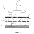
- Fig. 2 shows a schematic view of an inspection apparatus according to a second embodiment of the invention.
- the inspection apparatus 1 comprises an array of electron emitters 2 emitting a plurality of primary electron beams 5 which are focussed by means of a substantially uniform magnetic field.
- the plurality of primary electron beams 5 propagate through apertures 9 in a thin sheet like plate 8 comprising phosphor material.
- Secondary electron beams 10 are collected and converted to optical beams 11 which propagate in the direction of the array of electron emitters 2 and traverse through an optically transparent layer 15 disposed above the emitters 2.
- the optical beams 11 are focussed on detection means, such as a CCD camera, by means of an optical lens system 12.
- the detection means may also comprise other CCD sensors and/or a CMOS active pixel sensor, and/or a photodiode array.
- Fig. 3 shows a schematic view of an inspection apparatus according to a third embodiment of the invention.
- the inspection apparatus 1 comprises an emitter (not shown) emitting a plurality of primary photon beams 5a directed towards a specimen surface 3.
- An optical lens system 6a focuses the primary optical beams 5a onto loci 7 on the specimen surface 3.
- the primary beam 5a is relatively broad.
- a secondary, photoinduced electron beam 10a is emitted which contains spatial information of the surface being impinged by the relatively broad primary beam 5a and which passes through an electronic lens 16 arranged in the centre of the optical lens system 6a.
- the secondary electron beam 10a is collected and converted to an optical beam, and subsequently detected by photodetectors (not shown).
- the information relative to the specimen surface 3 is obtained by processing and imaging the spatial distribution of the detected optical beam, as the optical beams contains spatial information of the surface structure in the relatively broad loci 7.
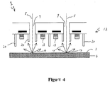
- Fig. 4 shows a schematic view of an inspection apparatus according to a fourth embodiment of the invention.
- the emission process of the plurality of primary beams 5 as well as lens systems are identical to the process and lens systems described under reference to Fig. 1.
- a micro electro mechanical system (MEMS) 17 is disposed between the emitter and the specimen surface 3.
- the MEMS 17 comprises an array of diodes 18 interspersed with apertures 9 to allow transmittance of the primary electron beams 5.
- a secondary electron beam 10 is detected by a diode 18.
- Each detecting area 19 in which a diode 18 is disposed is preferably equipped with electrodes 20 to increase the collecting angle by electrostatic focussing.
- Electrodes 20 also serve to prevent crosstalk between backscattered beams from neighbouring detecting areas 19. Additionally, there is space for embedded electronics to perform some 'on-detector' arithmetic data processing. For instance, addition and subtraction of symmetrically placed diodes 18 gives respectively compositional and topological information; these operations can be implemented on the MEMS 17. For data transport to peripheral instruments the MEMS advantageously might be implemented with a CCD-grid like array, so that an order of a million diodes may be read separately.
- the step of detecting the optical beam is accomplished at a location within a volume being traversed by the plurality of primary beams, as the diodes 18 on the MEMS 17 might convert the secondary beam into an optical beam and subsequently detect the optical beam.
- detection is carried out near the surface 3 of the specimen 4, thereby increasing the quality of the measurement detection of the inspection apparatus 1.
- the design of the apparatus may be simplified due to the omission of detection instruments outside the volume enclosing the space being traversed by the plurality of primary beams. It is noted, however, that it is also possible to convert the collected secondary beams directly to an electronic signal without generating an optical signal.
- a method of inspecting a specimen surface may comprise the steps of generating a plurality of primary beams directed towards the specimen surface, focussing the plurality of primary beams onto respective loci on the specimen surface, collecting a plurality of secondary beams of charged particles originating from the specimen surface upon incidence of the primary beams, and converting at least one of the collected secondary beams directly into an electronic signal.
- the primary electron beams are arranged in such a way that the plurality of primary beams propagate in a substantially parallel direction, so that mutual interaction of the primary beams is avoided and each of the primary beams is focussed onto a single locus on the specimen surface.
- the plurality of primary beams can also be tilted, such that two or more primary beams are focussed onto a single locus, for example, to enhance specific features of the specimen being inspected.
Landscapes
- Chemical & Material Sciences (AREA)
- Analytical Chemistry (AREA)
- General Health & Medical Sciences (AREA)
- Life Sciences & Earth Sciences (AREA)
- Health & Medical Sciences (AREA)
- Biochemistry (AREA)
- Physics & Mathematics (AREA)
- General Physics & Mathematics (AREA)
- Immunology (AREA)
- Pathology (AREA)
- Analysing Materials By The Use Of Radiation (AREA)
- Investigating, Analyzing Materials By Fluorescence Or Luminescence (AREA)
- Length-Measuring Devices Using Wave Or Particle Radiation (AREA)
- Testing Or Measuring Of Semiconductors Or The Like (AREA)
Abstract
The invention relates to a method of inspecting a specimen surface. The method comprises the steps of generating a plurality of primary beams directed towards the specimen surface, focussing the plurality of primary beams onto respective loci on the specimen surface, collecting a plurality of secondary beams of charged particles originating from the specimen surface upon incidence of the primary beams, converting at least one of the collected secondary beams into an optical beam, and detecting the optical beam.
Description
- The invention relates to a method of inspecting a specimen surface, comprising the steps of generating a plurality of primary beams directed towards the specimen surface, focussing the plurality of primary beams onto respective loci on the specimen surface, and collecting a plurality of secondary beams of charged particles originating from the specimen surface upon incidence of the primary beams.
- Such a method is known from e.g. patent publication US 6 465 783, disclosing methods and apparatus for inspecting semi-conductor wafers and other types of specimens, such as masks, using parallel charged particle beams, e.g. electron beams. An emitter array, including a plurality of charged-particle-beam emitters produces a plurality of primary beams that propagate along a substantially parallel direction. The primary beams pass simultaneously through projection lenses so as to cause the beams to be focused onto respective loci on the surface of the specimen so as to cause each locus to emit backscattered and/or secondary electrons, i.e. electrons generated by a secondary process. The backscattered and/or secondary electrons are collected and detected by a secondary-electron array including multiple detector units. Each detector unit collects and detects secondary electrons emitted from a respective locus to obtain information from the surface of the semi-conductor wafer or other type of specimen.
- During manufacture of integrated circuits it is necessary to inspect at various stages the substrate for defects. Inspection tools are indispensable for improving the yield in the semiconductor manufacturing process. The requirements of inspection machines are prescribed in international recognized documents which dictate ever increasing sensitivities for future years.
- A well-known inspection method which in practice does not suffer the resolution limit of optical microscopy is an inspection technique using a scanning electron beam to inspect wafers created in the semiconductor industry. In conventional electron beam inspection machines, a raster scan over the sample is performed with a single focussed electron probe. On irradiation with an electron probe, the substrate emits backscattered electrons and secondary electrons, from the point of incidence that can subsequently be detected with an electron detector, and the presence of any defects can be determined from the resulting pattern of backscattered or secondary electrons. The electron detector typically comprises a scintillator which collects electrons, a light guide for guiding photons, and a photon detector.
- The resolution capability of such a single electron beam system exceeds that of optical techniques, yet the long scanning time per wafer results in a very low throughput. Higher productivity can only be obtained by increasing the current because faster scanning while maintaining the same current leads to prohibitive decrease in signal-to-noise ratio. However, an increase of current occurs at the cost of resolution since Coulomb interactions (mutual repulsion of electrons) in the electron beam increase the minimum possible probe size. Hence, the amount of current in a scanning probe may be limited, thus reducing the scanning speed of the electron beam system to undesired values.
- Consequently, a technique with a single electron beam is impractical for production level inspection in the semiconductor industry. Instead, it is used for supplementary defect inspection of single defects that must be inspected at higher resolution.
- From the condition that a minimum signal-to-noise ratio is required it can be seen that the productivity of an inspection technique is proportional to the current that can be detected while maintaining resolution. The productivity of a single beam inspection machine can thus be increased by using multiple electron beams in parallel, as disclosed in e.g. patent publication US 6 465 783. Simply put, a machine with ten beams increases the productivity ten-fold and so on. Regardless of practical difficulties, the productivity of a multi beam system is highest if the footprint of the substrate (say a 300 mm wafer) is filled with as many individual beams as possible. For a practical system, the inspection field should be significantly smaller than 300 mm. A smaller field gives the possibility to use the full productivity enhancement over a small region of the wafer, for instance a single die. A larger field leads to the unwanted side effect that some of the beams are not used in the inspection process efficiency. Thus, when choosing between two different multi-beam systems with an equal number of beams, the one with the smaller footprint is the preferred system. For such systems it is crucial that each beam has its own electron detector in such a manner that cross talk between the various detectors can be neglected. One of the factors limiting the multiplicity are the dimensions of the electron detectors and the electrical means to transport the electronic information which is contained in the secondary electron beams, especially in the case of a multitude of primary beams.
- It is an object of the invention to provide a method according to the preamble, whereby the disadvantages identified above are reduced. In particular, the invention aims at obtaining a method of inspecting a specimen surface, wherein the multiplicity limitation is reduced. According to a first aspect of the present invention, there is provided a method of inspecting a specimen surface, comprising the steps of generating a plurality of primary beams directed towards the specimen surface, focussing the plurality of primary beams onto respective loci on the specimen surface, collecting a plurality of secondary beams of charged particles originating from the specimen surface upon incidence of the primary beams, converting at least one of the collected secondary beams into an optical beam, and detecting the optical beam.
- By converting at least one of the collected secondary beams into an optical beam, and by detecting the optical beam, it is not longer necessary to detect the secondary beam at a location near the surface of the specimen where interference of the secondary beams is minimal. Since the characteristics of the optical beam can also be determined at another location, more space is available for retrieving the information which is originally present in the secondary beam, so that more freedom with respect to the detection system, inclusive data transport means, is obtained. On the other hand, the information which is carried by the secondary particle beam may be detected more compactly. As a consequence, the plurality of primary beams can be arranged closer to each other, thereby reducing the multiplicity limitations of the conventional inspecting method and enhancing the productivity of the inspection apparatus.
- It is noted that in the context of this application a specimen surface encompasses the top layer of the specimen including material just below the boundary plane of the specimen.
- It is further noted that that the optical beam resulting from the converting step in the method according to the invention propagates at least initially in a non-waveguiding structure.
- In a preferred embodiment according to the invention, the step of converting the collected secondary beam into the optical beam is accomplished by means of fluorescent material. Advantageously, the fluorescent material does not impose requirements with respect to a minimum distance between the individual primary beams. Thus, the distance between the primary beams can be minimized. Further, the converting step can be achieved in a relatively cheap manner.
- In further preferred embodiment of to the invention, the step of detecting the optical beam is accomplished in a detection region outside of a volume enclosing the space being traversed by the plurality of primary beams. In this way, advantage is taken from the fact that the optical beam can pass the primary beams without substantial interference, so that the optical beam can be detected in a region that is not restricted by conditions determined by the geometry of the primary beams. As a consequence, the primary beams can be positioned even closer to each other, resulting in an even faster inspecting method and apparatus.
- It is noted that in the above-mentioned embodiment also the problem is reduced of designing the data transport system from the detection means to means for further processing and interpreting means. Due to the desired scanning speed of the inspecting apparatus, high speed data connection means may be required, such as coaxial cables, which in a conventional multi beam apparatus can limit a minimum distance between individual beams. By detecting the optical beams in a detection region outside of the volume enclosed by the space being traversed by the plurality of primary beams, designing parameters with respect to the high speed data connection are relaxed, thus allowing an ever smaller distance between the individual primary beams.
- By focussing the optical beam onto a detection system in the detection region, e.g. by means of a lens system, the detection of the optical beam can be carried out more accurately, thereby improving the performance of the inspecting method and apparatus.
- According to a second aspect of the present invention, there is provided an apparatus for inspecting a specimen surface, comprising at least one emitter arranged to emit a plurality of primary beams directed towards the specimen surface, focussing means arranged to focus the plurality of primary beams onto respective loci on the specimen surface, collecting means for collecting a plurality of secondary beams of charged particles originating from the specimen surface upon incidence of the primary beams, converting means for converting at least one of the collected secondary beams into an optical beam, and detection means for detecting the optical beam.
- According to a third aspect of the present invention, there is provided a use of fluorescent material in the method of inspecting a specimen surface according to claim 1 for converting the collected beam of secondary particles into the optical beam.
- According to a fourth aspect of the present invention, there is provided a method of inspecting a specimen surface, comprising the steps of generating a plurality of primary beams directed towards the specimen surface, focussing the plurality of primary beams onto respective loci on the specimen surface, collecting a plurality of secondary beams of charged particles originating from the specimen surface upon incidence of the primary beams, and converting at least one of the collected secondary beams directly into an electronic signal
- According to a fifth aspect of the present invention, there is provided an apparatus for inspecting a specimen surface, comprising at least one emitter arranged to emit a plurality of primary beams directed towards the specimen surface, focussing means arranged to focus the plurality of primary beams onto respective loci on the specimen surface, collecting means for collecting a plurality of secondary beams of charged particles originating from the specimen surface upon incidence of the primary beams, and converting means for converting at least one of the collected secondary beams directly into an electronic signal.
- Other advantageous embodiments according to the invention are described in the following claims.
- By way of example only, embodiments of the present invention will now be described with reference to the accompanying figures in which
- Fig. 1 shows a schematic view of an apparatus according to a first embodiment of the invention;
- Fig. 2 shows a schematic view of an apparatus according to a second embodiment of the invention;
- Fig. 3 shows a schematic view of an apparatus according to a third embodiment of the invention; and
- Fig. 4 shows a schematic view of an apparatus according to a fourth embodiment of the invention.
- The figures are merely schematic views of preferred embodiments according to the invention. In the figures, equal or corresponding parts are referred to by the same reference numbers.
- Figure 1 shows a schematic view of an apparatus 1 for inspecting a specimen surface according to a first embodiment of the invention. The inspection apparatus 1 comprises an
electron emitter 2 emitting, in use, a plurality ofprimary electron beams 5, which are directed towards asurface 3 of aspecimen 4 disposed on a table (not shown) of the apparatus 1. Further, the inspection apparatus 1 comprises focussing means embodied as a electron lens system comprising a cascade of lenses 6 to focus the plurality ofprimary beams 5 ontorespective loci 7 on thespecimen surface 3. In one of the focus planes A of the plurality ofprimary beams 5 between theelectron emitter 2 and thespecimen surface 3, a thin sheet like plate 8 comprising phosphor material is disposed. The thin sheet 8 comprisesapertures 9, so that theprimary beams 5 are allowed to pass. By positioning the plate 8 in one of the focus planes A, the dimensions of the apertures may remain minimal, resulting in a maximum surface for converting secondary electron beams into optical beams, as will be explained later. - Upon incidence of the
primary beams 5 onto therespective loci 7 on thespecimen surface 3 secondary electrons and backscattered electrons forming a plurality ofsecondary beams 10 originate from thespecimen surface 3. Thesecondary beams 10 are not focussed in theapertures 9 but rather than passing through theapertures 9 they strike the plate 8 which collects the electrons and converts asecondary beam 10 into an optical beam 11 which is focussed by means of anoptical lens system 12 onto detection means, embodied as an array ofphotodetectors 13. By interpreting the signals detected at the array ofphotodetectors 13 information from thespecimen surface 3 at theloci 7 may be revealed. The inspection apparatus 1 can be used as an inspection tool during manufacturing of chips or after the manufacturing steps have been completed. By adjusting theloci 7 on which theprimary beams 5 are focussed, the inspection apparatus can entirely or partly scan thespecimen surface 3. Adjustment of theloci 7 can be accomplished by e.g. moving thespecimen 4 and/or by repositioning of theprimary beams 5. - The lenses 6 of the focussing means can be implemented as micro lenses, comprising conducting aperture plates. These can be manufactured using standard micromachining fabrication techniques. However, the focussing means may also comprise magnetic fields generated by magnet coils.
- Preferably, an electrostatic field is generated between the
specimen surface 3 and the plate 8 in order to accelerate electrons in thesecondary beam 10 and to avoid interference or crosstalk between different secondary beams. - By an appropriate choice of the focal planes of the
optical lens system 12, theinitial beam diameter 14 of theoptical beam 12 is smaller than the beam diameter at a location where thephotodetectors 13 are disposed 15, thereby improving the quality of the optical beam detection and/or relaxing system requirements for thephotodetectors 13. As an alternative, theoptical beam 12 may be guided by means of an optical guide, such as an optical fibre, thereby saving space and relaxing positioning requirements for thephotodetectors 13. It is, of course, also possible to combine an optical lens system with an optical fibre structure. The array ofphotodetectors 13 comprise a CCD camera. However, in an alternative embodiment, the detection means may be implemented in another way, e.g. by using a CMOS image chip with or without active pixel sensors. The detection means may also comprise photodiodes in combination with or without photomultipliers. - In a preferred embodiment, a minimum distance is provided between the primary beams, because it has been found that due to the beam width of the
secondary beams 10 interference ofsecondary beams 10 result in loss of information. In other words, according to an embodiment of the invention, the secondary beams are detected separately from one another, i.e., without any substantial overlap between the secondary beams. - Instead of a phosphor material, the thin sheet like plate 8 may also comprise other fluorescent materials or YAG-materials having the property that the material converts an incident electron beam into an optical beam. Instead of using fluorescent material for converting the
secondary beam 10 into the optical beam 11, it is also possible to utilize electrochromic films, i.e. films that change colour on exposure to electron beam radiation, or current detectors driving LED's or lasers. In case of the former, the contrast is determined by the difference in electron beam intensity on the electrochromic film, yet the signal can be determined by an intense light source reflecting on the film towards thephotodetectors 13. In this manner the problem of detecting a low number of photons for each incident backscattered or secondary electron of thesecondary beam 10 is resolved. Electrochromic films are known for usage in smart windows incorporating the modulation of incoming light. Fast devices that allow utilization in LCD-like displays are among the other possibilities. - Instead of positioning the thin plate 8 in one of the focus planes A, it is also possible to position the plate 8 closer to the specimen surface, so that overlap of the
secondary beams 10 is reduced or further avoided. It is noted that the plate 8 with the phosphor material integrates the functionality of collecting thesecondary beams 10 and converting asecondary beam 10 into an optical beam 11. As an example, the plate 8 comprises a glass plate supporting a coated phosphor layer. However, it is also possible to implement the above-mentioned functionalities separately, e.g. by providing an auxiliary structure for improving the properties of receiving the individual secondary electron beams. As an example, this can be implemented by means of strips on the plate 8 which are not transparent for thesecondary beams 10 and extend towards thespecimen surface 3 in order to separate and collect electrons of adjacentsecondary beams 10. Further, the collecting angle of thesecondary beams 10 can be increased, reducing crosstalk, either by using small electrodes disposed in between theapertures 9, or by intentionally leaving a part disposed between the apertures electrically isolated. With such an arrangement, the isolated part charges up and the resulting fields act as an electron channel forcing backscattered electrons towards the closest phosphor site. - If the main structure is a glass plate, the
apertures 9 for theprimary beams 5 may have to be drilled or etched. The glass plate must be thick enough to have sufficient mechanical rigidity. Whilst this has repercussions on the minimal diameter, and consequently the 'detector spacing', of theapertures 9, it has been found that the rigidity of the glass plate may be improved by using a segmented glass plate, which is relatively thin and may be embedded in a grid for extra support. As an alternative, the plate 8 may have other configurations, e.g. it may be configured as a curved surface. - The inspection apparatus, shown in Fig. 1, comprises a single electron emitter illuminating an
aperture array 14, thus emitting the plurality of primary electron beams. An alternative construction may be formed by providing an array of electron emitters. - Fig. 2 shows a schematic view of an inspection apparatus according to a second embodiment of the invention. The inspection apparatus 1 comprises an array of
electron emitters 2 emitting a plurality ofprimary electron beams 5 which are focussed by means of a substantially uniform magnetic field. The plurality ofprimary electron beams 5 propagate throughapertures 9 in a thin sheet like plate 8 comprising phosphor material.Secondary electron beams 10 are collected and converted to optical beams 11 which propagate in the direction of the array ofelectron emitters 2 and traverse through an opticallytransparent layer 15 disposed above theemitters 2. Further, the optical beams 11 are focussed on detection means, such as a CCD camera, by means of anoptical lens system 12. The detection means may also comprise other CCD sensors and/or a CMOS active pixel sensor, and/or a photodiode array. - Fig. 3 shows a schematic view of an inspection apparatus according to a third embodiment of the invention. The inspection apparatus 1 comprises an emitter (not shown) emitting a plurality of primary photon beams 5a directed towards a
specimen surface 3. An optical lens system 6a focuses the primary optical beams 5a ontoloci 7 on thespecimen surface 3. In contrast to the preceding embodiments according to the invention, the primary beam 5a is relatively broad. Upon incidence of the primary beam 5a, a secondary, photoinduced electron beam 10a is emitted which contains spatial information of the surface being impinged by the relatively broad primary beam 5a and which passes through anelectronic lens 16 arranged in the centre of the optical lens system 6a. Again, as in the previous embodiments, the secondary electron beam 10a is collected and converted to an optical beam, and subsequently detected by photodetectors (not shown). The information relative to thespecimen surface 3 is obtained by processing and imaging the spatial distribution of the detected optical beam, as the optical beams contains spatial information of the surface structure in the relativelybroad loci 7. - Fig. 4 shows a schematic view of an inspection apparatus according to a fourth embodiment of the invention. In the inspection apparatus 1 the emission process of the plurality of
primary beams 5 as well as lens systems are identical to the process and lens systems described under reference to Fig. 1. However, instead of the thin sheet like plate 8, a micro electro mechanical system (MEMS) 17 is disposed between the emitter and thespecimen surface 3. TheMEMS 17 comprises an array ofdiodes 18 interspersed withapertures 9 to allow transmittance of the primary electron beams 5. Asecondary electron beam 10 is detected by adiode 18. Each detecting area 19 in which adiode 18 is disposed is preferably equipped withelectrodes 20 to increase the collecting angle by electrostatic focussing. Theseelectrodes 20 also serve to prevent crosstalk between backscattered beams from neighbouring detecting areas 19. Additionally, there is space for embedded electronics to perform some 'on-detector' arithmetic data processing. For instance, addition and subtraction of symmetrically placeddiodes 18 gives respectively compositional and topological information; these operations can be implemented on theMEMS 17. For data transport to peripheral instruments the MEMS advantageously might be implemented with a CCD-grid like array, so that an order of a million diodes may be read separately. - In the embodiment described under reference to Fig. 4, the step of detecting the optical beam is accomplished at a location within a volume being traversed by the plurality of primary beams, as the
diodes 18 on theMEMS 17 might convert the secondary beam into an optical beam and subsequently detect the optical beam. In this process, detection is carried out near thesurface 3 of thespecimen 4, thereby increasing the quality of the measurement detection of the inspection apparatus 1. In essence, the design of the apparatus may be simplified due to the omission of detection instruments outside the volume enclosing the space being traversed by the plurality of primary beams. It is noted, however, that it is also possible to convert the collected secondary beams directly to an electronic signal without generating an optical signal. In particular, a method of inspecting a specimen surface may comprise the steps of generating a plurality of primary beams directed towards the specimen surface, focussing the plurality of primary beams onto respective loci on the specimen surface, collecting a plurality of secondary beams of charged particles originating from the specimen surface upon incidence of the primary beams, and converting at least one of the collected secondary beams directly into an electronic signal. - The invention is not restricted to the embodiments described herein. It will be understood that many variants are possible. In the described methods and apparatuses, the primary electron beams are arranged in such a way that the plurality of primary beams propagate in a substantially parallel direction, so that mutual interaction of the primary beams is avoided and each of the primary beams is focussed onto a single locus on the specimen surface. However, the plurality of primary beams can also be tilted, such that two or more primary beams are focussed onto a single locus, for example, to enhance specific features of the specimen being inspected.
- Further such variants will be obvious for the man skilled in the art and are considered to lie within the scope of the invention as formulated in the following claims.
Claims (21)
- Method of inspecting a specimen surface, comprising the steps of- generating a plurality of primary beams directed towards the specimen surface;- focussing the plurality of primary beams onto respective loci on the specimen surface;- collecting a plurality of secondary beams of charged particles originating from the specimen surface upon incidence of the primary beams;- converting at least one of the collected secondary beams into an optical beam; and- detecting the optical beam.
- Method according to claim 1, wherein the step of converting the collected secondary beam into the optical beam is accomplished by means of fluorescent material.
- Method according to claim 2 or claim 3, wherein the step of detecting the optical beam is accomplished in a detection region outside of a volume enclosing the space being traversed by the plurality of primary beams.
- Method according to any preceding claim, comprising the step of focussing the optical beam onto a detection system in the detection region.
- Method according to claim 4, wherein the initial beam diameter of the optical beam is smaller than the beam diameter at a location where the detection system is disposed.
- Method according to any of the preceding claims 1-2, wherein the step of detecting the optical beam is accomplished at a location within a volume being traversed by the plurality of primary beams.
- Method according to claim 6, wherein the step of detecting the optical beams is accomplished by means of a micro electro mechanical system.
- Apparatus for inspecting a specimen surface, comprising- at least one emitter arranged to emit a plurality of primary beams directed towards the specimen surface;- focussing means arranged to focus the plurality of primary beams onto respective loci on the specimen surface;- collecting means for collecting a plurality of secondary beams of charged particles originating from the specimen surface upon incidence of the primary beams;- converting means for converting at least one of the collected secondary beams into an optical beam; and- detection means for detecting the optical beam.
- Apparatus according to claim 8, wherein the converting means comprises fluorescent material.
- Apparatus according to claim 8 or 9, wherein the collecting means and the converting means are integrated.
- Apparatus according to any of the preceding claims 8-10, wherein the converting means comprises phosphor material.
- Apparatus according to any of the preceding claims 8-11, wherein the detection means are located outside of a volume enclosing the space being traversed by the plurality of primary beams.
- Apparatus according to any of the preceding claims 8-12, further comprising optical focussing means for focussing the optical beams to the detection means.
- Apparatus according to any of the preceding claims 8-13, further comprising a micro electro mechanical system for detecting the optical beams at a location within a volume being traversed by the plurality of primary beams.
- Apparatus according to any of the preceding claims, wherein a minimum distance is provided between the primary beams, so that any substantial overlap between the secondary beams is avoided.
- Use of fluorescent material in the method of inspecting a specimen surface according to claim 1 for converting the collected beam of secondary particles into the optical beam.
- Use of fluorescent material according to claim 16, wherein the fluorescent material comprises phosphor material.
- Use of fluorescent material according to claim 17, wherein the phosphor material is embodied in a thin sheet like plate.
- Use of fluorescent material according to any of the preceding claims 16-18, wherein the fluorescent screen is disposed between the at least one emitter and the specimen surface, and is constructed such that the primary beams are allowed to pass.
- Method of inspecting a specimen surface comprising the steps of:- generating a plurality of primary beams directed towards the specimen surface;- focussing the plurality of primary beams onto respective loci on the specimen surface;- collecting a plurality of secondary beams of charged particles originating from the specimen surface upon incidence of the primary beams; and- converting at least one of the collected secondary beams directly into an electronic signal.
- Apparatus for inspecting a specimen surface, comprising- at least one emitter arranged to emit a plurality of primary beams directed towards the specimen surface;- focussing means arranged to focus the plurality of primary beams onto respective loci on the specimen surface;- collecting means for collecting a plurality of secondary beams of charged particles originating from the specimen surface upon incidence of the primary beams; and- converting means for converting at least one of the collected secondary beams directly into an electronic signal.
Priority Applications (8)
| Application Number | Priority Date | Filing Date | Title |
|---|---|---|---|
| EP04077130A EP1619495A1 (en) | 2004-07-23 | 2004-07-23 | Method and Apparatus for inspecting a specimen surface and use of fluorescent materials |
| KR1020077004070A KR101330368B1 (en) | 2004-07-23 | 2005-07-21 | Method and apparatus for inspecting a specimen surface |
| PCT/NL2005/000529 WO2006009444A2 (en) | 2004-07-23 | 2005-07-21 | Method and apparatus for inspecting a specimen surface and use of fluorescent materials |
| EP05764078A EP1779097A2 (en) | 2004-07-23 | 2005-07-21 | Method and apparatus for inspecting a specimen surface and use of fluorescent materials |
| JP2007522450A JP5179176B2 (en) | 2004-07-23 | 2005-07-21 | Method, apparatus for inspecting sample surface, and use of fluorescent material |
| CN2005800316018A CN101023342B (en) | 2004-07-23 | 2005-07-21 | Method of inspecting a specimen surface, apparatus and use of fluorescent material |
| US11/572,398 US7732762B2 (en) | 2004-07-23 | 2005-07-21 | Method of inspecting a specimen surface, apparatus and use of fluorescent material |
| IL180835A IL180835A (en) | 2004-07-23 | 2007-01-21 | Method and apparatus for inspecting a specimen surface and use of fluorescent materials |
Applications Claiming Priority (1)
| Application Number | Priority Date | Filing Date | Title |
|---|---|---|---|
| EP04077130A EP1619495A1 (en) | 2004-07-23 | 2004-07-23 | Method and Apparatus for inspecting a specimen surface and use of fluorescent materials |
Publications (1)
| Publication Number | Publication Date |
|---|---|
| EP1619495A1 true EP1619495A1 (en) | 2006-01-25 |
Family
ID=34928396
Family Applications (2)
| Application Number | Title | Priority Date | Filing Date |
|---|---|---|---|
| EP04077130A Withdrawn EP1619495A1 (en) | 2004-07-23 | 2004-07-23 | Method and Apparatus for inspecting a specimen surface and use of fluorescent materials |
| EP05764078A Withdrawn EP1779097A2 (en) | 2004-07-23 | 2005-07-21 | Method and apparatus for inspecting a specimen surface and use of fluorescent materials |
Family Applications After (1)
| Application Number | Title | Priority Date | Filing Date |
|---|---|---|---|
| EP05764078A Withdrawn EP1779097A2 (en) | 2004-07-23 | 2005-07-21 | Method and apparatus for inspecting a specimen surface and use of fluorescent materials |
Country Status (7)
| Country | Link |
|---|---|
| US (1) | US7732762B2 (en) |
| EP (2) | EP1619495A1 (en) |
| JP (1) | JP5179176B2 (en) |
| KR (1) | KR101330368B1 (en) |
| CN (1) | CN101023342B (en) |
| IL (1) | IL180835A (en) |
| WO (1) | WO2006009444A2 (en) |
Cited By (10)
| Publication number | Priority date | Publication date | Assignee | Title |
|---|---|---|---|---|
| WO2010014850A3 (en) * | 2008-08-01 | 2010-04-01 | Direct Electron, Lp | Apparatus and method including a direct bombardment detector and a secondary detector for use in electron microscopy |
| EP3579263A1 (en) * | 2018-06-07 | 2019-12-11 | FEI Company | Improved multi-beam electron microscope |
| CN110634722A (en) * | 2018-06-25 | 2019-12-31 | Fei 公司 | Multiple Beam Charged Particle Imaging Facility |
| EP3937204A1 (en) * | 2020-07-06 | 2022-01-12 | ASML Netherlands B.V. | Inspection apparatus |
| EP3937205A1 (en) * | 2020-07-06 | 2022-01-12 | ASML Netherlands B.V. | Charged-particle multi-beam column, charged-particle multi-beam column array, inspection method |
| WO2022008462A1 (en) * | 2020-07-06 | 2022-01-13 | Asml Netherlands B.V. | A detector substrate for use in a charged particle multi-beam assessment tool |
| EP4020565A1 (en) * | 2020-12-23 | 2022-06-29 | ASML Netherlands B.V. | Detector substrate, an inspection apparatus and method of sample assessment |
| EP4075476A1 (en) * | 2021-04-15 | 2022-10-19 | ASML Netherlands B.V. | Electron-optical device |
| US11798783B2 (en) | 2020-01-06 | 2023-10-24 | Asml Netherlands B.V. | Charged particle assessment tool, inspection method |
| WO2026068198A1 (en) * | 2024-09-27 | 2026-04-02 | Carl Zeiss Multisem Gmbh | Multi-aperture array for manipulating a plurality of first individual charged particle beams as well as multiple particle beam system comprising the multi-aperture array |
Families Citing this family (22)
| Publication number | Priority date | Publication date | Assignee | Title |
|---|---|---|---|---|
| EP1619495A1 (en) | 2004-07-23 | 2006-01-25 | Nederlandse Organisatie voor toegepast-natuurwetenschappelijk Onderzoek TNO | Method and Apparatus for inspecting a specimen surface and use of fluorescent materials |
| JP4878501B2 (en) * | 2006-05-25 | 2012-02-15 | 株式会社日立ハイテクノロジーズ | Charged particle beam application equipment |
| US7518127B2 (en) * | 2006-12-22 | 2009-04-14 | Von Zanthier Joachim | Sub-wavelength imaging and irradiation with entangled particles |
| JP4597207B2 (en) * | 2008-03-31 | 2010-12-15 | 株式会社日立ハイテクノロジーズ | Scanning electron microscope |
| BR112013033596A2 (en) * | 2011-04-14 | 2017-01-24 | Boehringer Ingelheim Int | method for modifying the radiation characteristic of an excited emitter |
| EP2654069B1 (en) * | 2012-04-16 | 2016-02-24 | ICT Integrated Circuit Testing Gesellschaft für Halbleiterprüftechnik mbH | Multi channel detector, optics therefore and method of operating thereof |
| EP2654068B1 (en) * | 2012-04-16 | 2017-05-17 | ICT Integrated Circuit Testing Gesellschaft für Halbleiterprüftechnik mbH | Switchable multi perspective detector, optics therefore and method of operating thereof |
| US9042516B2 (en) * | 2012-10-09 | 2015-05-26 | The Boeing Company | Nondestructive examination of structures having embedded particles |
| NL2009696C2 (en) * | 2012-10-25 | 2014-04-29 | Univ Delft Tech | Apparatus and method for inspecting a surface of a sample. |
| EP2816585A1 (en) * | 2013-06-17 | 2014-12-24 | ICT Integrated Circuit Testing Gesellschaft für Halbleiterprüftechnik mbH | Charged particle beam system and method of operating thereof |
| NL2013411B1 (en) | 2014-09-04 | 2016-09-27 | Univ Delft Tech | Multi electron beam inspection apparatus. |
| US20180364563A1 (en) * | 2017-06-20 | 2018-12-20 | Applied Materials, Inc. | Method and apparatus for inspecting a sample |
| KR20200044100A (en) | 2017-09-29 | 2020-04-28 | 에이에스엠엘 네델란즈 비.브이. | Multi-cell detector for charged particles |
| US10395887B1 (en) * | 2018-02-20 | 2019-08-27 | Technische Universiteit Delft | Apparatus and method for inspecting a surface of a sample, using a multi-beam charged particle column |
| CN113272934B (en) * | 2018-12-28 | 2024-11-29 | Asml荷兰有限公司 | Device for multiple charged particle beams |
| EP3716312A1 (en) * | 2019-03-28 | 2020-09-30 | FEI Company | Charged particle beam device for inspection of a specimen with a plurality of charged particle beamlets |
| US12080513B2 (en) * | 2019-08-14 | 2024-09-03 | Asml Netherlands B.V. | Cross-talk cancellation in multiple charged-particle beam inspection |
| EP3971939A1 (en) * | 2020-09-17 | 2022-03-23 | ASML Netherlands B.V. | Charged particle assessment tool, inspection method |
| IL300807A (en) | 2020-09-17 | 2023-04-01 | Asml Netherlands Bv | Charged particle assessment tool, inspection method |
| WO2022135926A1 (en) * | 2020-12-23 | 2022-06-30 | Asml Netherlands B.V. | Electron lens |
| IL303983A (en) * | 2020-12-23 | 2023-08-01 | Asml Netherlands Bv | Charged particle optical device |
| US11430633B2 (en) * | 2020-12-29 | 2022-08-30 | Fei Company | Illumination apertures for extended sample lifetimes in helical tomography |
Citations (6)
| Publication number | Priority date | Publication date | Assignee | Title |
|---|---|---|---|---|
| DE19546142A1 (en) * | 1995-11-28 | 1997-06-05 | Roentec Gmbh | Semiconductor X=ray detector for high resolution electron microscopy |
| CH688665A5 (en) * | 1993-01-25 | 1997-12-31 | Zlatimir Dimcovski | Imaging process for biological material and operating in real=time |
| US20020089595A1 (en) * | 1994-06-01 | 2002-07-11 | Risto Olavi Orava | Radiation imaging system with imaging devices arranged in a mosaic |
| US6465783B1 (en) * | 1999-06-24 | 2002-10-15 | Nikon Corporation | High-throughput specimen-inspection apparatus and methods utilizing multiple parallel charged particle beams and an array of multiple secondary-electron-detectors |
| EP1271605A1 (en) * | 2000-11-02 | 2003-01-02 | Ebara Corporation | Electron beam apparatus and method for manufacturing semiconductor device comprising the apparatus |
| US20030164460A1 (en) * | 1997-10-02 | 2003-09-04 | Hitachi, Ltd. | Patterned wafer inspection method and apparatus therefor |
Family Cites Families (20)
| Publication number | Priority date | Publication date | Assignee | Title |
|---|---|---|---|---|
| JPS63175325A (en) | 1987-01-16 | 1988-07-19 | Jeol Ltd | Charged particle detecting device |
| JPH01220352A (en) * | 1988-02-26 | 1989-09-04 | Hitachi Ltd | Scanning electron microscopes and similar equipment |
| GB2229854B (en) * | 1989-03-28 | 1993-10-27 | Robinson Vivian N E | Backscattered electron detector |
| JP3774953B2 (en) * | 1995-10-19 | 2006-05-17 | 株式会社日立製作所 | Scanning electron microscope |
| JP3494152B2 (en) * | 1995-10-19 | 2004-02-03 | 株式会社日立製作所 | Scanning electron microscope |
| JP3434165B2 (en) * | 1997-04-18 | 2003-08-04 | 株式会社日立製作所 | Scanning electron microscope |
| JP4069545B2 (en) * | 1999-05-19 | 2008-04-02 | 株式会社日立製作所 | Electron microscope method, electron microscope array biological sample inspection method and biological inspection apparatus using the same |
| WO2001060456A1 (en) * | 2000-02-19 | 2001-08-23 | Ion Diagnostics, Inc. | Multi-beam multi-column electron beam inspection system |
| EP1339100A1 (en) * | 2000-12-01 | 2003-08-27 | Ebara Corporation | Inspection method and apparatus using electron beam, and device production method using it |
| US6775452B2 (en) * | 2001-05-18 | 2004-08-10 | Applied Materials, Inc. | Phosphor coated waveguide for efficient collection of electron-generated photons |
| US6750455B2 (en) * | 2001-07-02 | 2004-06-15 | Applied Materials, Inc. | Method and apparatus for multiple charged particle beams |
| JP3782692B2 (en) * | 2001-09-06 | 2006-06-07 | 株式会社東芝 | Electron beam apparatus and semiconductor device manufacturing method using the apparatus |
| CN2588367Y (en) * | 2002-12-25 | 2003-11-26 | 北京有色金属研究总院 | Digital image receiving processing system for transmission electron microscope |
| DE10301579A1 (en) * | 2003-01-16 | 2004-07-29 | Leo Elektronenmikroskopie Gmbh | Electron beam device and detector arrangement |
| US7138629B2 (en) | 2003-04-22 | 2006-11-21 | Ebara Corporation | Testing apparatus using charged particles and device manufacturing method using the testing apparatus |
| EP2575144B1 (en) * | 2003-09-05 | 2017-07-12 | Carl Zeiss Microscopy GmbH | Particle-optical systems and arrangements and particle-optical components for such systems and arrangements |
| US7531812B2 (en) * | 2003-10-27 | 2009-05-12 | Politechnika Wroclawska | Method and system for the directional detection of electrons in a scanning electron microscope |
| US7385197B2 (en) * | 2004-07-08 | 2008-06-10 | Ebara Corporation | Electron beam apparatus and a device manufacturing method using the same apparatus |
| EP1619495A1 (en) | 2004-07-23 | 2006-01-25 | Nederlandse Organisatie voor toegepast-natuurwetenschappelijk Onderzoek TNO | Method and Apparatus for inspecting a specimen surface and use of fluorescent materials |
| US7324323B2 (en) * | 2005-01-13 | 2008-01-29 | Lucent Technologies Inc. | Photo-sensitive MEMS structure |
-
2004
- 2004-07-23 EP EP04077130A patent/EP1619495A1/en not_active Withdrawn
-
2005
- 2005-07-21 JP JP2007522450A patent/JP5179176B2/en not_active Expired - Fee Related
- 2005-07-21 KR KR1020077004070A patent/KR101330368B1/en not_active Expired - Fee Related
- 2005-07-21 EP EP05764078A patent/EP1779097A2/en not_active Withdrawn
- 2005-07-21 WO PCT/NL2005/000529 patent/WO2006009444A2/en not_active Ceased
- 2005-07-21 CN CN2005800316018A patent/CN101023342B/en not_active Expired - Fee Related
- 2005-07-21 US US11/572,398 patent/US7732762B2/en active Active
-
2007
- 2007-01-21 IL IL180835A patent/IL180835A/en not_active IP Right Cessation
Patent Citations (6)
| Publication number | Priority date | Publication date | Assignee | Title |
|---|---|---|---|---|
| CH688665A5 (en) * | 1993-01-25 | 1997-12-31 | Zlatimir Dimcovski | Imaging process for biological material and operating in real=time |
| US20020089595A1 (en) * | 1994-06-01 | 2002-07-11 | Risto Olavi Orava | Radiation imaging system with imaging devices arranged in a mosaic |
| DE19546142A1 (en) * | 1995-11-28 | 1997-06-05 | Roentec Gmbh | Semiconductor X=ray detector for high resolution electron microscopy |
| US20030164460A1 (en) * | 1997-10-02 | 2003-09-04 | Hitachi, Ltd. | Patterned wafer inspection method and apparatus therefor |
| US6465783B1 (en) * | 1999-06-24 | 2002-10-15 | Nikon Corporation | High-throughput specimen-inspection apparatus and methods utilizing multiple parallel charged particle beams and an array of multiple secondary-electron-detectors |
| EP1271605A1 (en) * | 2000-11-02 | 2003-01-02 | Ebara Corporation | Electron beam apparatus and method for manufacturing semiconductor device comprising the apparatus |
Non-Patent Citations (2)
| Title |
|---|
| H. SUNAOSHI ET AL: "In-Situ beam position monitoring system for electron beam lithography", SPIE PROCEEDINGS, vol. 3777, July 1999 (1999-07-01), DENVER, COLORADO, pages 15 - 22, XP002306788 * |
| NIEDRIG H ET AL: "Information depth and spatial resolution in BSE microtomography in SEM", NUCLEAR INSTRUMENTS & METHODS IN PHYSICS RESEARCH, SECTION - B: BEAM INTERACTIONS WITH MATERIALS AND ATOMS, NORTH-HOLLAND PUBLISHING COMPANY. AMSTERDAM, NL, vol. 142, no. 4, 1 August 1998 (1998-08-01), pages 523 - 534, XP004141580, ISSN: 0168-583X * |
Cited By (17)
| Publication number | Priority date | Publication date | Assignee | Title |
|---|---|---|---|---|
| WO2010014850A3 (en) * | 2008-08-01 | 2010-04-01 | Direct Electron, Lp | Apparatus and method including a direct bombardment detector and a secondary detector for use in electron microscopy |
| US7952073B2 (en) | 2008-08-01 | 2011-05-31 | Direct Electron, Lp | Apparatus and method including a direct bombardment detector and a secondary detector for use in electron microscopy |
| EP3579263A1 (en) * | 2018-06-07 | 2019-12-11 | FEI Company | Improved multi-beam electron microscope |
| US10937627B2 (en) | 2018-06-07 | 2021-03-02 | Fei Company | Multi-beam electron microscope |
| CN110634722A (en) * | 2018-06-25 | 2019-12-31 | Fei 公司 | Multiple Beam Charged Particle Imaging Facility |
| US12548735B2 (en) | 2020-01-06 | 2026-02-10 | Asml Netherlands B.V. | Charged particle assessment tool, inspection method |
| US11984295B2 (en) | 2020-01-06 | 2024-05-14 | Asml Netherlands B.V. | Charged particle assessment tool, inspection method |
| US11798783B2 (en) | 2020-01-06 | 2023-10-24 | Asml Netherlands B.V. | Charged particle assessment tool, inspection method |
| WO2022008462A1 (en) * | 2020-07-06 | 2022-01-13 | Asml Netherlands B.V. | A detector substrate for use in a charged particle multi-beam assessment tool |
| CN115769332A (en) * | 2020-07-06 | 2023-03-07 | Asml荷兰有限公司 | Charged particle multi-beam train, charged particle multi-beam train array, inspection method |
| WO2022008286A1 (en) * | 2020-07-06 | 2022-01-13 | Asml Netherlands B.V. | Charged-particle multi-beam column, charged-particle multi-beam column array, inspection method |
| EP3937205A1 (en) * | 2020-07-06 | 2022-01-12 | ASML Netherlands B.V. | Charged-particle multi-beam column, charged-particle multi-beam column array, inspection method |
| EP3937204A1 (en) * | 2020-07-06 | 2022-01-12 | ASML Netherlands B.V. | Inspection apparatus |
| EP4020565A1 (en) * | 2020-12-23 | 2022-06-29 | ASML Netherlands B.V. | Detector substrate, an inspection apparatus and method of sample assessment |
| EP4075476A1 (en) * | 2021-04-15 | 2022-10-19 | ASML Netherlands B.V. | Electron-optical device |
| WO2022218634A1 (en) * | 2021-04-15 | 2022-10-20 | Asml Netherlands B.V. | Electron-optical device |
| WO2026068198A1 (en) * | 2024-09-27 | 2026-04-02 | Carl Zeiss Multisem Gmbh | Multi-aperture array for manipulating a plurality of first individual charged particle beams as well as multiple particle beam system comprising the multi-aperture array |
Also Published As
| Publication number | Publication date |
|---|---|
| WO2006009444A9 (en) | 2007-06-21 |
| JP2008507690A (en) | 2008-03-13 |
| KR101330368B1 (en) | 2013-11-15 |
| CN101023342A (en) | 2007-08-22 |
| IL180835A0 (en) | 2007-06-03 |
| WO2006009444A2 (en) | 2006-01-26 |
| EP1779097A2 (en) | 2007-05-02 |
| US20070272856A1 (en) | 2007-11-29 |
| WO2006009444A3 (en) | 2006-04-06 |
| IL180835A (en) | 2015-06-30 |
| CN101023342B (en) | 2011-03-23 |
| US7732762B2 (en) | 2010-06-08 |
| JP5179176B2 (en) | 2013-04-10 |
| KR20070085210A (en) | 2007-08-27 |
Similar Documents
| Publication | Publication Date | Title |
|---|---|---|
| US7732762B2 (en) | Method of inspecting a specimen surface, apparatus and use of fluorescent material | |
| US10395887B1 (en) | Apparatus and method for inspecting a surface of a sample, using a multi-beam charged particle column | |
| EP1439566B1 (en) | Charged particle beam apparatus and method for operating the same | |
| JP5102580B2 (en) | Charged particle beam application equipment | |
| US7714287B1 (en) | Apparatus and method for obtaining topographical dark-field images in a scanning electron microscope | |
| EP2190002B1 (en) | Method for detecting a fine geometry | |
| KR20230021128A (en) | Charged Particle Multi-Beam Column, Charged Particle Multi-Beam Column Array, Inspection Method | |
| US8164059B2 (en) | In-chamber electron detector | |
| KR20220083798A (en) | Method and Charged Particle Beam Device for Inspecting Specimens | |
| EP2487703A1 (en) | Detector for use in charged-particle microscopy | |
| JP2014238962A (en) | Electron beam apparatus | |
| TWI809358B (en) | Charged particle detector, charged particle beam device, radiation detector and radiation detection device | |
| KR20240001152A (en) | Charged particle evaluation system and method | |
| US20200312610A1 (en) | Charged particle beam device for inspection of a specimen with a plurality of charged particle beamlets | |
| TWI827124B (en) | Charged particle apparatus and method | |
| JPH0982261A (en) | electronic microscope | |
| US20240321547A1 (en) | Charged-particle optical device | |
| JP5822614B2 (en) | Inspection device | |
| JP3107593B2 (en) | Pattern inspection equipment | |
| WO2021074260A1 (en) | Systems and methods of profiling charged-particle beams | |
| KR102845787B1 (en) | charged particle beam device | |
| TWI918321B (en) | Charged particle assessment apparatus, inspection method | |
| JP2006032278A (en) | Electron beam device, and device manufacturing method using the same | |
| TW202533269A (en) | High-voltage discharge detection in a charged particle system | |
| WO2025202056A1 (en) | Multi electron-beam system for inspection with backscattered electrons |
Legal Events
| Date | Code | Title | Description |
|---|---|---|---|
| PUAI | Public reference made under article 153(3) epc to a published international application that has entered the european phase |
Free format text: ORIGINAL CODE: 0009012 |
|
| AK | Designated contracting states |
Kind code of ref document: A1 Designated state(s): AT BE BG CH CY CZ DE DK EE ES FI FR GB GR HU IE IT LI LU MC NL PL PT RO SE SI SK TR |
|
| AX | Request for extension of the european patent |
Extension state: AL HR LT LV MK |
|
| AKX | Designation fees paid | ||
| REG | Reference to a national code |
Ref country code: DE Ref legal event code: 8566 |
|
| STAA | Information on the status of an ep patent application or granted ep patent |
Free format text: STATUS: THE APPLICATION IS DEEMED TO BE WITHDRAWN |
|
| 18D | Application deemed to be withdrawn |
Effective date: 20060726 |