EP1615270A1 - Radioactive ray detector - Google Patents
Radioactive ray detector Download PDFInfo
- Publication number
- EP1615270A1 EP1615270A1 EP04726812A EP04726812A EP1615270A1 EP 1615270 A1 EP1615270 A1 EP 1615270A1 EP 04726812 A EP04726812 A EP 04726812A EP 04726812 A EP04726812 A EP 04726812A EP 1615270 A1 EP1615270 A1 EP 1615270A1
- Authority
- EP
- European Patent Office
- Prior art keywords
- radiation
- wiring substrate
- hole
- signal processing
- signal
- Prior art date
- Legal status (The legal status is an assumption and is not a legal conclusion. Google has not performed a legal analysis and makes no representation as to the accuracy of the status listed.)
- Withdrawn
Links
- 230000002285 radioactive effect Effects 0.000 title 1
- 239000000758 substrate Substances 0.000 claims abstract description 244
- 230000005855 radiation Effects 0.000 claims abstract description 205
- 239000011521 glass Substances 0.000 claims abstract description 100
- 239000000463 material Substances 0.000 claims abstract description 46
- 239000004065 semiconductor Substances 0.000 claims description 13
- 230000002093 peripheral effect Effects 0.000 description 11
- 229910052751 metal Inorganic materials 0.000 description 9
- 239000002184 metal Substances 0.000 description 9
- 230000000903 blocking effect Effects 0.000 description 7
- PXHVJJICTQNCMI-UHFFFAOYSA-N Nickel Chemical compound [Ni] PXHVJJICTQNCMI-UHFFFAOYSA-N 0.000 description 6
- 239000005355 lead glass Substances 0.000 description 6
- 238000000034 method Methods 0.000 description 6
- 239000000853 adhesive Substances 0.000 description 4
- 230000001070 adhesive effect Effects 0.000 description 4
- 230000015556 catabolic process Effects 0.000 description 4
- 239000010949 copper Substances 0.000 description 4
- 238000006731 degradation reaction Methods 0.000 description 4
- 238000001514 detection method Methods 0.000 description 4
- 239000010931 gold Substances 0.000 description 4
- 230000003287 optical effect Effects 0.000 description 4
- 238000009429 electrical wiring Methods 0.000 description 3
- 230000035945 sensitivity Effects 0.000 description 3
- RYGMFSIKBFXOCR-UHFFFAOYSA-N Copper Chemical compound [Cu] RYGMFSIKBFXOCR-UHFFFAOYSA-N 0.000 description 2
- BQCADISMDOOEFD-UHFFFAOYSA-N Silver Chemical compound [Ag] BQCADISMDOOEFD-UHFFFAOYSA-N 0.000 description 2
- 239000011651 chromium Substances 0.000 description 2
- 239000002131 composite material Substances 0.000 description 2
- 229910052802 copper Inorganic materials 0.000 description 2
- 230000000694 effects Effects 0.000 description 2
- PCHJSUWPFVWCPO-UHFFFAOYSA-N gold Chemical compound [Au] PCHJSUWPFVWCPO-UHFFFAOYSA-N 0.000 description 2
- 229910052737 gold Inorganic materials 0.000 description 2
- 229910052759 nickel Inorganic materials 0.000 description 2
- 239000002245 particle Substances 0.000 description 2
- 239000011347 resin Substances 0.000 description 2
- 229920005989 resin Polymers 0.000 description 2
- 229910052709 silver Inorganic materials 0.000 description 2
- 239000004332 silver Substances 0.000 description 2
- 229910000679 solder Inorganic materials 0.000 description 2
- 238000011144 upstream manufacturing Methods 0.000 description 2
- 229910004613 CdTe Inorganic materials 0.000 description 1
- 229910004611 CdZnTe Inorganic materials 0.000 description 1
- VYZAMTAEIAYCRO-UHFFFAOYSA-N Chromium Chemical compound [Cr] VYZAMTAEIAYCRO-UHFFFAOYSA-N 0.000 description 1
- XUIMIQQOPSSXEZ-UHFFFAOYSA-N Silicon Chemical compound [Si] XUIMIQQOPSSXEZ-UHFFFAOYSA-N 0.000 description 1
- NRTOMJZYCJJWKI-UHFFFAOYSA-N Titanium nitride Chemical compound [Ti]#N NRTOMJZYCJJWKI-UHFFFAOYSA-N 0.000 description 1
- 239000000956 alloy Substances 0.000 description 1
- 229910045601 alloy Inorganic materials 0.000 description 1
- 229910052782 aluminium Inorganic materials 0.000 description 1
- XAGFODPZIPBFFR-UHFFFAOYSA-N aluminium Chemical compound [Al] XAGFODPZIPBFFR-UHFFFAOYSA-N 0.000 description 1
- 230000005540 biological transmission Effects 0.000 description 1
- 229910052804 chromium Inorganic materials 0.000 description 1
- 239000011231 conductive filler Substances 0.000 description 1
- 239000004020 conductor Substances 0.000 description 1
- 238000000151 deposition Methods 0.000 description 1
- 230000008021 deposition Effects 0.000 description 1
- 239000003365 glass fiber Substances 0.000 description 1
- 238000004519 manufacturing process Methods 0.000 description 1
- 150000002739 metals Chemical class 0.000 description 1
- 238000002161 passivation Methods 0.000 description 1
- 238000000059 patterning Methods 0.000 description 1
- 230000000149 penetrating effect Effects 0.000 description 1
- 238000007747 plating Methods 0.000 description 1
- 229910052710 silicon Inorganic materials 0.000 description 1
- 239000010703 silicon Substances 0.000 description 1
- 238000004544 sputter deposition Methods 0.000 description 1
- 239000000126 substance Substances 0.000 description 1
- 238000007740 vapor deposition Methods 0.000 description 1
Images





Classifications
-
- G—PHYSICS
- G01—MEASURING; TESTING
- G01T—MEASUREMENT OF NUCLEAR OR X-RADIATION
- G01T1/00—Measuring X-radiation, gamma radiation, corpuscular radiation, or cosmic radiation
- G01T1/16—Measuring radiation intensity
- G01T1/20—Measuring radiation intensity with scintillation detectors
- G01T1/2018—Scintillation-photodiode combinations
- G01T1/20187—Position of the scintillator with respect to the photodiode, e.g. photodiode surrounding the crystal, the crystal surrounding the photodiode, shape or size of the scintillator
-
- G—PHYSICS
- G01—MEASURING; TESTING
- G01T—MEASUREMENT OF NUCLEAR OR X-RADIATION
- G01T1/00—Measuring X-radiation, gamma radiation, corpuscular radiation, or cosmic radiation
- G01T1/16—Measuring radiation intensity
- G01T1/20—Measuring radiation intensity with scintillation detectors
- G01T1/2018—Scintillation-photodiode combinations
- G01T1/20185—Coupling means between the photodiode and the scintillator, e.g. optical couplings using adhesives with wavelength-shifting fibres
-
- G—PHYSICS
- G01—MEASURING; TESTING
- G01T—MEASUREMENT OF NUCLEAR OR X-RADIATION
- G01T1/00—Measuring X-radiation, gamma radiation, corpuscular radiation, or cosmic radiation
- G01T1/16—Measuring radiation intensity
- G01T1/20—Measuring radiation intensity with scintillation detectors
- G01T1/2018—Scintillation-photodiode combinations
- G01T1/20188—Auxiliary details, e.g. casings or cooling
- G01T1/2019—Shielding against direct hits
-
- G—PHYSICS
- G01—MEASURING; TESTING
- G01T—MEASUREMENT OF NUCLEAR OR X-RADIATION
- G01T1/00—Measuring X-radiation, gamma radiation, corpuscular radiation, or cosmic radiation
- G01T1/16—Measuring radiation intensity
- G01T1/24—Measuring radiation intensity with semiconductor detectors
-
- H—ELECTRICITY
- H10—SEMICONDUCTOR DEVICES; ELECTRIC SOLID-STATE DEVICES NOT OTHERWISE PROVIDED FOR
- H10F—INORGANIC SEMICONDUCTOR DEVICES SENSITIVE TO INFRARED RADIATION, LIGHT, ELECTROMAGNETIC RADIATION OF SHORTER WAVELENGTH OR CORPUSCULAR RADIATION
- H10F39/00—Integrated devices, or assemblies of multiple devices, comprising at least one element covered by group H10F30/00, e.g. radiation detectors comprising photodiode arrays
- H10F39/10—Integrated devices
- H10F39/12—Image sensors
- H10F39/18—Complementary metal-oxide-semiconductor [CMOS] image sensors; Photodiode array image sensors
- H10F39/189—X-ray, gamma-ray or corpuscular radiation imagers
- H10F39/1895—X-ray, gamma-ray or corpuscular radiation imagers of the hybrid type
-
- H—ELECTRICITY
- H10—SEMICONDUCTOR DEVICES; ELECTRIC SOLID-STATE DEVICES NOT OTHERWISE PROVIDED FOR
- H10F—INORGANIC SEMICONDUCTOR DEVICES SENSITIVE TO INFRARED RADIATION, LIGHT, ELECTROMAGNETIC RADIATION OF SHORTER WAVELENGTH OR CORPUSCULAR RADIATION
- H10F39/00—Integrated devices, or assemblies of multiple devices, comprising at least one element covered by group H10F30/00, e.g. radiation detectors comprising photodiode arrays
- H10F39/80—Constructional details of image sensors
- H10F39/809—Constructional details of image sensors of hybrid image sensors
-
- H—ELECTRICITY
- H10—SEMICONDUCTOR DEVICES; ELECTRIC SOLID-STATE DEVICES NOT OTHERWISE PROVIDED FOR
- H10F—INORGANIC SEMICONDUCTOR DEVICES SENSITIVE TO INFRARED RADIATION, LIGHT, ELECTROMAGNETIC RADIATION OF SHORTER WAVELENGTH OR CORPUSCULAR RADIATION
- H10F77/00—Constructional details of devices covered by this subclass
- H10F77/40—Optical elements or arrangements
- H10F77/496—Luminescent members, e.g. fluorescent sheets
Definitions
- This invention relates to a radiation detector in which employed is a wiring substrate with a conduction path for guiding an electric signal.
- Radiation detectors for use with CT sensors include a detector with a scintillator placed on the light-incident surface of a semiconductor photodetecting element array such as a photodiode array.
- a radiation detector when the radiation to be detected is made incident on the scintillator, such as X-rays, gamma rays, or charged particles, scintillation light is generated by the radiation in the scintillator. The scintillation light is then detected with the semiconductor photodetecting elements, thereby allowing the radiation to be detected.
- the photodetecting element array is also provided with a signal processing element for processing a detected signal that is outputted from each photodetecting element.
- the photodetecting element and the signal processing element can be electrically connected therebetween using various types of wirings, or conduction paths provided in a wiring substrate (e.g., see Japanese Patent Application Laid-Open No. H8-330469).
- part of radiation made incident on the scintillator normally transmits the scintillator and the photodetecting element array.
- the scintillator, the photodetecting element array, the wiring substrate, and the signal processing element may be located along a predetermined alignment direction, and this arrangement raises a problem that the radiation having transmitted the scintillator and the like transmits the wiring substrate to be made incident upon the signal processing element located downstream of the arrangement.
- the radiation made incident on the signal processing element in this manner would result in damage to the signal processing element due to the radiation, thereby causing degradation in the characteristics of the radiation detector such as sensitivity, reliability, or life.
- an object of the invention is to provide a radiation detector which suppresses radiation made incident on signal processing means located downstream of a wiring substrate.
- a radiation detector includes (1) radiation detecting means for detecting incident radiation to output a detected signal, (2) signal processing means for processing the detected signal from the radiation detecting means, and (3) a wiring substrate section having a wiring substrate with a conduction path provided for guiding the detected signal between a signal input surface and a signal output surface, the radiation detecting means and the signal processing means being connected to the signal input surface and the signal output surface, respectively, wherein (4) the wiring substrate includes a glass substrate formed of a predetermined glass material having a radiation shielding function and provided with a through hole, and a conductive member provided in the through hole to serve as the conduction path for establishing electrical continuity between the signal input surface and the signal output surface, and (5) the radiation detecting means, the wiring substrate section, and the signal processing means are located in this order along a predetermined alignment direction, with the signal processing means being disposed with respect to the wiring substrate within an area other than an area on an extension of the through hole.
- the wiring substrate used to electrically connect between the radiation detecting means and the signal processing means is formed of a glass substrate of a predetermined glass material.
- the signal processing means is disposed relative to the through hole of the conduction path provided in the glass substrate so as to be dislocated from an area where the through hole is provided, thereby allowing the signal processing means not to be seen through the through hole.
- a portion with no through hole in the wiring substrate allows the glass material thereof to suppress radiation transmitting from the signal input surface to the signal output surface. Even another portion with a through hole in the wiring substrate will also allow radiation having passed through the through hole not to be made incident on the signal processing means. This realizes a radiation detector which suppresses radiation made incident on the signal processing means irrespective of the presence of the through hole in the wiring substrate.
- the wiring substrate preferably has an electrode pad provided at a predetermined portion facing the signal processing means on the signal output surface of the glass substrate and a wiring for electrically connecting between the electrode pad and the corresponding conductive member. This allows for transferring an electric signal from the radiation detecting means to the signal processing means via the conductive member provided in the wiring substrate, the wiring, and the electrode pad. It is also acceptable to employ other arrangements.
- a radiation detector includes (1) radiation detecting means for detecting incident radiation to output a detected signal, (2) signal processing means for processing the detected signal from the radiation detecting means, and (3) a wiring substrate section having a wiring substrate with a conduction path provided for guiding the detected signal between a signal input surface and a signal output surface, the radiation detecting means and the signal processing means being connected to the signal input surface and the signal output surface, respectively, wherein (4) the wiring substrate includes a glass substrate formed of a predetermined glass material having a radiation shielding function and provided with a through hole, and a conductive member provided in the through hole to serve as the conduction path for establishing electrical continuity between the signal input surface and the signal output surface, and (5) the radiation detecting means, the wiring substrate section, and the signal processing means are located in that order along a predetermined alignment direction, while an opening of the through hole provided in the wiring substrate from the signal input surface to the signal output surface is blocked with a shield member having a radiation shielding function.
- the wiring substrate used to electrically connect between the radiation detecting means and the signal processing means is formed of a glass substrate of a predetermined glass material.
- the shield member for blocking the opening of the through hole in the wiring substrate is provided for the through hole of the conduction path provided in the glass substrate, thereby allowing the signal processing means not to be seen through the through hole.
- a portion with no through hole in the wiring substrate allows the glass material thereof to suppress radiation transmitting from the signal input surface to the signal output surface.
- Another portion with a through hole in the wiring substrate will also allow the shield member to suppress radiation passing through the through hole.
- the shield member is preferably configured such that a predetermined shield material having a radiation shielding function is filled in the through hole.
- the shield member is preferably a bump electrode which is formed of a predetermined shield material having a radiation shielding function and which is electrically connected to the conductive member provided in the through hole.
- the glass substrate is preferably formed of a glass material that contains lead. This allows for effectively suppressing radiation transmitting the wiring substrate. It is also acceptable to employ a substrate formed of another glass material having a radiation shielding function.
- the conductive member can be formed on an inner wall of the through hole provided in the glass substrate.
- the conductive member can also be filled in the through hole provided in the glass substrate.
- the glass substrate of the wiring substrate is preferably provided with a plurality of through holes while a plurality of hollow glass members that are open at both ends are fused together and integrally formed. It is also acceptable to use other glass substrates configured in a variety of ways.
- the radiation detecting means may include a scintillator for generating scintillation light by radiation made incident, and a semiconductor photodetecting element for detecting the scintillation light from the scintillator.
- the radiation detecting means may include a semiconductor detecting element for detecting radiation made incident thereon.
- the wiring substrate section and the radiation detecting means or the wiring substrate section and the signal processing means be electrically connected to each other via a bump electrode.
- a metal bump electrode can be used as electrical connection means, thereby electrically connecting between each portion in a preferred manner.
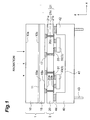
- FIG. 1 is a sectional side view illustrating the sectional structure of a radiation detector according to a first embodiment
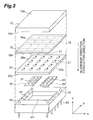
- FIG. 2 is an exploded perspective view illustrating the configuration of the radiation detector shown in FIG. 1;
- FIGS. 3A and 3B are plan views illustrating (A) the configuration of a signal input surface of a wiring substrate, and (B) the configuration of a signal output surface thereof;
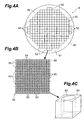
- FIGS. 4A to 4C are views illustrating an example of a glass substrate provided with a plurality of through holes
- FIGS. 5A and 5B are views illustrating an example of the configuration of a conductive member provided in the through hole of the wiring substrate
- FIGS. 6A and 6B are views illustrating another example of the configuration of a conductive member provided in the through hole of the wiring substrate
- FIG. 7 is a sectional side view illustrating the sectional structure of a radiation detector according to a second embodiment
- FIG. 8 is an exploded perspective view illustrating the configuration of the radiation detector shown in FIG. 7;
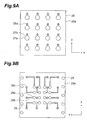
- FIGS. 9A and 9B are plan views illustrating (A) the configuration of a signal input surface of a wiring substrate, and (B) the configuration of a signal output surface thereof;
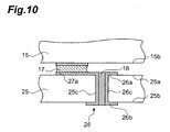
- FIG. 10 is a view illustrating an example of the configuration of a through hole and a shield member in the wiring substrate
- FIG. 11 is a view illustrating another example of the configuration of a through hole and a shield member in the wiring substrate
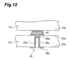
- FIG. 12 is a view illustrating still another example of the configuration of a through hole and a shield member in the wiring substrate
- FIG. 13 is a sectional side view illustrating the sectional structure of a radiation detector according to a third embodiment.
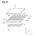
- FIG. 14 is an exploded perspective view illustrating the configuration of the radiation detector shown in FIG. 13.
- FIG. 1 is a sectional side view illustrating the sectional structure of a radiation detector according to a first embodiment of the present invention.
- FIG. 2 is an exploded perspective view illustrating components in the configuration of the radiation detector shown in FIG. 1.
- radiation is incident along the direction of z-axis, and two axes orthogonal to the z-axis are the x-axis and y-axis.
- the negative direction of the z-axis is the conduction direction from a signal input surface to a signal output surface in the wiring substrate, and the alignment direction of the components in the radiation detector.
- the radiation detector shown in FIG. 1 includes a radiation detecting section 1, a wiring substrate section 2, and a signal processing section 3. As shown in FIG. 2, these components are arranged in that order from the upstream side (the upper side in the figure) to the downstream side (the lower side) along the predetermined alignment direction.
- the radiation detecting section 1 is detecting means for detecting a radiation to be detected made incident upon the radiation detector, such as X-rays, gamma rays, or charged particles, to output a detected signal of an electric signal corresponding thereto.
- the radiation detecting section 1 includes a scintillator 10 and a photodiode array 15.
- the scintillator 10 forms the upstream portion of the radiation detecting section 1, with its upper surface 10a serving as a radiation- incident surface of the radiation detector.
- the scintillator 10 generates scintillation light of a predetermined wavelength by radiation made incident from the incident surface 10a.
- the photodiode array (PD array) 15 forms the downstream portion of the radiation detecting section 1.
- the PD array 15 is a photodetecting element array in which a plurality of photodiodes (PDs) which are semiconductor photodetecting elements for detecting scintillation light from the scintillator 10 are arrayed.
- the lower surface of the scintillator 10 serving as a light output surface 10b and the upper surface of the PD array 15 serving as a light-incident surface 15a are optically connected to each other with an optical adhesive 11 that transmits the scintillation light.
- the lower surface 15b of the PD array 15 serves as a signal output surface for outputting a detected signal from each of the photodiodes 16.
- sixteen bump electrodes 17 for outputting the detected signal are disposed in an array of 4 ⁇ 4 corresponding to each of the photodiodes 16.
- the substrate electrode of the photodiodes is formed with a bump electrode on the lower surface 15b of the PD array.
- a drive electrode, a substrate electrode, and an electrode pad for video output and a bump electrode are also required.
- the wiring substrate section 2 Downstream of the radiation detecting section 1, provided is the wiring substrate section 2.
- the wiring substrate section 2 has the wiring substrate 20 formed with a conduction path for guiding an electric signal between the signal input surface and the signal output surface.
- the wiring substrate 20 is formed of a glass substrate of a predetermined glass material having a radiation shielding function. Such a glass material preferably includes, e.g., lead glass containing lead.
- FIGS. 3A and 3B are plan views each illustrating the configuration of the wiring substrate 20; FIG. 3A showing the upper surface thereof as a signal input surface 20a, FIG. 3B showing the lower surface thereof as a signal output surface 20b.
- the glass substrate constituting the wiring substrate 20 includes a plurality of through holes 20c formed between the input surface 20a and the output surface 20b. Also provided in the respective through holes 20c is a conductive member 21 that serves as a conduction path through which electrical continuity is established between the input surface 20a and the output surface 20b.
- These through holes 20c and conductive members 21 are formed with the same pitch as those of the bump electrodes 17 at the PD array 15.
- the conductive member 21 includes a conducting portion 21c formed inside the through hole 20c, an input portion 21 a formed on the outer peripheral portion of the through hole 20c on the input surface 20a in connection with the conducting portion 21c, and an output portion 21b formed on the outer peripheral portion of the through hole 20c on the output surface 20b in connection with the conducting portion 21 c.
- the electrode pad 22a is positioned corresponding to the bump electrode 17 on the output surface 15b of the PD array 15.
- the electrode pad 22a is also electrically connected to the corresponding input portion 21 a of the conductive member 21 via a wiring 22b.
- This configuration allows the photodiode 16 for outputting a detected signal of the PD array 15 to be electrically connected via the bump electrode 17, the electrode pad 22a, and the wiring 22b to the conductive member 21 which is a conduction path that transfers the detected signal in the wiring substrate 20.
- electrode pads 23a and 23c are formed on the output surface 20b of the wiring substrate 20 in addition to the output portion 21b of the conductive member 21.
- the electrode pads 23a and 23c are each electrically connected to the output portion 21b of the corresponding conductive member 21 via wirings 23b and 23d, respectively.
- the electrode pad 24 is used for connection to a housing 40, which is to be described later. Although not illustrated, part or all of the electrode pads 24 are electrically connected to a predetermined portion of the signal processing element.
- the signal processing section 3 and the housing (package) 40 are located downstream of the wiring substrate section 2.
- the signal processing section 3 includes the two signal processing elements 30 and 32 which are each provided with a signal processing circuit for processing the detected signal from the PD array 15 of the radiation detecting section 1.
- a signal processing element 30 is located at an area on the output surface 20b of the wiring substrate 20; the area is sandwiched between the four through holes disposed in the first column L 1 from the negative side along the x-axis (the left side when viewed from the radiation detecting section 1) and the four through holes disposed in the second column L 2 . As shown in FIG. 3B, the signal processing element 30 is disposed in an area between the columns L 1 and L 2 , the area excluding those on the extension of the through holes 20c on the columns L 1 and L 2 .
- eight electrode pads 23a are provided which are electrically connected to the corresponding conductive members 21 in the columns L 1 and L 2 via the wirings 23b.
- a signal processing element 32 is located at an area on the output surface 20b of the wiring substrate 20; the area is sandwiched between the four through holes disposed in the first column L 4 from the positive side along the x-axis (the right side when viewed from the radiation detecting section 1) and the four through holes disposed in the second column L 3 . As shown in FIG. 3B, the signal processing element 32 is disposed in an area between the columns L 3 and L 4 , the area excluding those on the extension of the through holes 20c on the columns L 3 and L 4 .
- eight electrode pads 23c are provided which are electrically connected to the corresponding conductive members 21 in the columns L 3 and L 4 via the wirings 23d.
- On the upper surface of the signal processing element 32 also provided are eight bump electrodes 33 at positions corresponding to the electrode pads 23c. This configuration allows the eight of the conductive members 21 of the wiring substrate 20 in the columns L 3 and L 4 to be electrically connected to the signal processing circuit provided in the signal processing element 32 via the output portions 21b, the wirings 23d, the electrode pads 23c, and the bump electrodes 33.
- the housing 40 is a holding member for integrally holding the radiation detecting section 1, the wiring substrate section 2, and the signal processing section 3.
- the housing 40 includes an element receiving portion 41 which is provided as a recessed portion on the upper surface thereof to receive the signal processing elements 30 and 32 therein, and a support portion 42 which is provided on the outer peripheral portion of the element receiving portion 41, connected to the electrode pads 24 of the wiring substrate 20 via bump electrodes 44, and supporting the radiation detecting section 1, the wiring substrate section 2, and the signal processing section 3.
- leads 43 used for inputting and outputting an electric signal from and to an external portion.
- radiation such as X-rays made incident upon the scintillator 10 of the radiation detecting section 1 will generate scintillation light in the scintillator 10, allowing the scintillation light to be made incident upon the photodiodes 16 of the PD array 15 via the optical adhesive 11.
- the photodiodes 16 detect this scintillation light to output electric signals as detected signals corresponding to the detection of the radiation.
- the detected signal outputted from each of the photodiodes 16 of the PD array 15 is sent to the signal processing elements 30 and 32 via the corresponding bump electrode 17, conductive member 21 of the wiring substrate 20, and bump electrodes 31 and 33 sequentially. Then, the signal processing circuit of the signal processing elements 30 and 32 performs the required signal processing on the detected signal.
- the wiring substrate 20 used for electrically connecting between the radiation detecting section 1 and the signal processing section 3 is formed of a glass substrate of a predetermined glass material. Additionally, the signal processing elements 30 and 32 of the signal processing section 3 are each dislocated from an area where the through hole 20c of the conduction path in the glass substrate is provided, thereby allowing the signal processing elements 30 and 32 not to be seen through the through hole 20c.
- a portion with no through hole 20c in the wiring substrate 20 allows the glass material thereof to suppress radiation transmitting from the signal input surface 20a to the signal output surface 20b. Even another portion with the through hole 20c in the wiring substrate 20 will also allow the radiation having passed through the through hole 20c not to be made incident upon the signal processing elements 30 and 32. This allows for suppressing the radiation made incident upon the signal processing section 3 irrespective of the presence of the through hole 20c in the wiring substrate 20, thereby realizing a radiation detector which can ensure that degradation resulting from damage due to radiation in characteristics such as sensitivity, reliability, and life is suppressed.
- a glass material containing lead as the glass material used for the glass substrate in the wiring substrate 20 of the wiring substrate section 2.
- Use of the lead glass will make it possible to effectively suppress the transmission of radiation through the wiring substrate section 2.
- the wiring substrate 20 employs a glass substrate in which the through hole 20c for forming the conductive member 21 serving as a conduction path is provided between the input surface 20a on the radiation detecting section 1 side and the output surface 20b on the signal processing section 3 side.
- a glass substrate for example, it is possible to use a glass substrate having a plurality of through holes while a plurality of hollow glass members that are open at both ends are fused together and integrally formed.
- FIGS. 4A to 4C are views illustrating an example of the above-mentioned glass substrate provided with a plurality of through holes.
- shown is a general example of the configuration of a glass substrate having a plurality of through holes. Accordingly, the glass substrate shown in FIGS. 4A to 4C has a shape and configuration different from those of the wiring substrate used in the radiation detector shown in FIG. 1.
- FIG. 4A is a plan view illustrating the configuration of the glass substrate
- FIG. 4B being a plan view illustrating the configuration of a multi-channel member included in the glass substrate
- FIG. 4C being a perspective view illustrating the configuration of the glass member included in the multi-channel member.
- FIGS. 4A to 4C show the glass substrate without a conductive member serving as a conduction path in the wiring substrate.
- a glass substrate 9 has a capillary substrate 90.
- the capillary substrate 90 includes a plurality of multi-channel members 92 having a plurality of through holes 93.
- the multi-channel members 92 are fused together and integrally formed while being disposed two-dimensionally within a peripheral member 91 formed of a glass material.
- such a capillary substrate 90 is integrally formed of a plurality of glass fibers, with the core glass portions being removed to thereby form the plurality of through holes 93.
- the multi-channel member 92 is configured such that a plurality of hollow glass members 95 that are open at both ends are fused together and integrally formed.
- the multi-channel member 92 has a square shape (e.g., about 1000 ⁇ m ⁇ 1000 ⁇ m) when viewed from a direction perpendicular to the upper and lower surfaces of the capillary substrate 90.
- the through hole 93 has a circular shape at its opening. For example, the inner diameter of the through hole 93 is about 6 ⁇ m.
- a glass material having a radiation shielding function e.g., a lead glass material is used as the glass material of the peripheral member 91 and the glass members 95 forming the capillary substrate 90.
- the wiring substrate 20 in the radiation detector shown in FIG. 1 for example, it is possible to use one in which a conductive member serving as a conduction path is formed in the through hole of the glass substrate configured as shown in FIGS. 4A to 4C. That is, in such a glass substrate configured in this manner, the shape of the substrate, the number of the through holes and their location and the like are set according to the configuration of the radiation detector.
- the conductive member serving as the conduction path is formed in the through hole provided in the glass substrate, and on each of its surfaces, an electrical wiring pattern comprised of respectively required electrodes and wirings is formed. It is thus possible to obtain a wiring substrate which is configured as shown in FIGS. 3A and 3B.
- FIGS. 5A and 5B are views illustrating an example of the configuration of the conductive member provided in the through hole of the wiring substrate, FIG. 5A being a top plan view, FIG. 5B being a cross-sectional view taken along arrows I-I.
- each of the through holes 20c is formed to have a circular cross-sectional shape with a center axis of an axis perpendicular to the input surface 20a and the output surface 20b of the wiring substrate 20.
- the conductive member 21 electrically connecting between the input surface 20a and the output surface 20b is provided in the through hole 20c as a member formed on the inner wall of the through hole 20c. That is, the conducting portion 21c is formed in the through hole 20c on the inner wall thereof. Additionally, on the outer peripheral portion of the through hole 20c on the input surface 20a, the input portion 21 a is formed in connection with the conducting portion 21 c. Furthermore, on the outer peripheral portion of the through hole 20c on the output surface 20b, formed is the output portion 21b in connection with the conducting portion 21c.
- the conducting portion 21c, the input portion 21a, and the output portion 21 b constitute the conductive member 21 serving as the conduction path in the wiring substrate 20.
- FIGS. 6A and 6B are views illustrating another example of the configuration of the conductive member provided in the through hole of the wiring substrate, FIG. 6A being a top plan view, FIG. 6B being a cross-sectional view taken along arrows II-II.
- a plurality of through holes 20c are formed in a two-dimensional array. As shown in FIG. 6B, each of the through holes 20c is formed to have a circular cross-sectional shape with a center axis of an axis perpendicular to the input surface 20a and the output surface 20b of the wiring substrate 20.
- the conductive member 21 electrically connecting between the input surface 20a and the output surface 20b is provided in the through hole 20c as a member filled in the through hole 20c. That is, the conducting portion 21c is filled in the through hole 20c. Additionally, on the outer peripheral portion of the through hole 20c on the input surface 20a, the input portion 21 a is formed in connection with the conducting portion 21 c. Furthermore, on the outer peripheral portion of the through hole 20c on the output surface 20b, the output portion 21b is formed in connection with the conducting portion 21c.
- the conducting portion 21c, the input portion 21 a, and the output portion 21b constitute the conductive member 21 serving as the conduction path in the first wiring substrate 20.
- the configuration shown in FIGS. 5A and 5B and FIGS. 6A and 6B can be used as the conductive member which is formed as the conduction path in the glass substrate having a plurality of through holes.
- the location of the conduction path in the glass substrate serving as the wiring substrate is preferably set according to the configuration of the radiation detector.
- such an arrangement may be configured such that of a plurality of through holes, a through hole located at a position necessary for a conduction path is selected using a mask or the like to form a conductive member.
- a through hole may also be selectively provided only at a position requiring a conduction path.
- the glass substrate used for the wiring substrate may not be limited to the arrangement shown in FIGS. 4A to 4C but may also employ other arrangements.
- a plurality of glass members each having a through hole are integrated into a multi-channel member, and a plurality of multi-channel members are integrated into a capillary substrate.
- a plurality of glass members may also be integrated directly into a capillary substrate. It is preferable to determine how the individual glass members and multi-channel members are shaped and arranged, and whether and how through holes are provided in each member, as appropriate in a preferred manner according to the arrangement of the conduction path.
- the through hole may also have a polygonal cross-sectional shape other than a circular one, e.g., a rectangular one.
- FIG. 1 A brief explanation will now be made of a method for manufacturing the radiation detector shown in FIG. 1 in accordance with its specific exemplary configuration.
- a glass substrate which is formed of a glass material such as lead glass having a radiation shielding function and with through holes at predetermined positions. Then, the conductive members serving as the conduction paths are formed in the through holes, and additionally, an electrical wiring pattern having respectively required electrodes and wirings is formed on both the input and output surfaces to fabricate the wiring substrate 20 used in the wiring substrate section 2.
- the conductive member 21 made up of the conducting portion 21c, the input portion 21 a, and the output portion 21b is formed in the through hole 20c provided in the glass substrate. Additionally, formed are the electrode pad 22a and the wiring 22b on the input surface 20a as well as the electrode pads 23a, 23c, and 24, and the wirings 23b and 23d on the output surface 20b, thereby providing the wiring substrate 20.
- the above-described conductive member and the electrical wiring pattern provided on the glass substrate can be formed of an electrically conductive metal layer of titanium nitride (TiN), nickel (Ni), aluminum (Al), chromium (Cr), copper (Cu), silver (Ag), gold (Au), or an alloy thereof.
- a metal layer may be a single metal layer, a composite film, or a layered film.
- the layer may be formed by providing a mask of a desired pattern on the glass substrate to form a metal film by vapor deposition, CVD, plating, or sputtering, and then by removing the mask.
- bump electrodes may be further formed on the wiring substrate 20.
- the wiring substrate section 2 of the wiring substrate 20 is fabricated as described above, then, the IC chips of the signal processing elements 30 and 32 with the bump electrodes 31 and 33 formed thereon are aligned with the electrode pads 23a and 23c provided on the output surface 20b of the wiring substrate 20, respectively, for physical and electrical connection therebetween. Furthermore, the PD array 15 with the bump electrodes 17 formed thereon is also aligned with the electrode pads 22a provided on the input surface 20a of the wiring substrate 20 for physical and electrical connection therebetween.
- the bump material to form the bump electrodes 31, 33, and 17 it is possible to use nickel (Ni), copper (Cu), silver (Ag), gold (Au), solder, resin containing an electrically conductive filler, or a composite material thereof. It is also acceptable to interpose an under-bump metal (UBM) between the bump electrode and the underlying electrode pad in order to prevent the metals from diffusing into each other or enhance their mutual contact.
- UBM under-bump metal
- the housing 40 having the bump electrodes 44 formed thereon is aligned with the electrode pads 24 provided on the output surface 20b of the wiring substrate 20 for physical and electrical connection therebetween. This allows for performing an input and output operation of a signal between an external circuit via the leads 43 provided on the housing 40. Furthermore, the scintillator 10 is implemented using the optical adhesive 11 on the light-incident surface 15a of the PD array 15, thereby providing the radiation detector shown in FIG.1.
- FIG. 7 is a sectional side view illustrating the sectional structure of a radiation detector according to a second embodiment.
- FIG. 8 is an exploded perspective view illustrating components in the configuration of the radiation detector shown in FIG. 7.
- the radiation detector shown in FIG. 7 includes the radiation detecting section 1, the wiring substrate section 2, the signal processing section 3, and the housing 40. Of these components, the configurations of the radiation detecting section 1 and the housing 40 are the same as those of the embodiment shown in FIG. 1.
- the wiring substrate section 2 is located downstream of the radiation detecting section 1.
- the wiring substrate section 2 has a wiring substrate 25 in which provided is a conduction path for guiding an electric signal between the signal input surface and the signal output surface.
- the wiring substrate 25 employs, as its substrate, a glass substrate formed of a predetermined glass material having a radiation shielding function.
- a glass substrate formed of a predetermined glass material having a radiation shielding function.
- FIGS. 9A and 9B are plan views each illustrating the configuration of the wiring substrate 25, FIG. 9A illustrating its upper surface as a signal input surface 25a, FIG. 9B illustrating its lower surface as a signal output surface 25b.
- the glass substrate constituting the wiring substrate 25 has a plurality of through holes 25c between the input surface 25a and the output surface 25b.
- Each of the through holes 25c is provided with a conductive member 26, which serves as a conduction path for electrically connecting between the input surface 25a and the output surface 25b.
- These through holes 25c and conductive members 26 are formed with the same pitch as those of the bump electrodes 17 in the PD array 15.
- the through holes and the conductive members for the substrate electrodes of the photodiodes are not illustrated.
- the conductive member 26 includes a conducting portion 26c formed inside the through hole 25c, an input portion 26a formed on the outer peripheral portion of the through hole 25c on the input surface 25a in connection with the conducting portion 26c, and an output portion 26b formed on the outer peripheral portion of the through hole 25c on the output surface 25b in connection with the conducting portion 26c.
- the electrode pad 27a is positioned corresponding to the bump electrode 17 on the output surface 15b of the PD array 15.
- the electrode pad 27a is also electrically connected to the corresponding input portion 26a of the conductive member 26 via a wiring 27b.
- This configuration allows the photodiode 16 for outputting a detected signal of the PD array 15 to be electrically connected via the bump electrode 17, the electrode pad 27a, and the wiring 27b to the conductive member 26 of the conduction path that transfers the detected signal in the wiring substrate 25.
- an electrode pad 28a is formed on the output surface 25b of the wiring substrate 25 in addition to the output portion 26b of the conductive member 26.
- the electrode pad 28a is electrically connected to the output portion 26b of the corresponding conductive member 26 via a wiring 28b.
- the electrode pad 29 is used for connection to the housing 40. Although not illustrated, part or all of the electrode pads 29 are electrically connected to a predetermined portion of the signal processing element.
- the portion excluding the conducting portion 26c inside the through hole 25c is filled with a shield member 18 of a predetermined shield material having a radiation shielding function.
- This configuration allows the opening of the through hole 25c leading from the signal input surface 25a of the wiring substrate 25 to the signal output surface 25b to be blocked with the shield member 18.
- the signal processing section 3 and the housing 40 are placed downstream of the wiring substrate section 2.
- the signal processing section 3 includes a signal processing element 34 which is provided with a signal processing circuit for processing the detected signal from the PD array 15 of the radiation detecting section 1.
- a bump electrode 35 On the upper surface of the signal processing element 34, there is provided a bump electrode 35.
- the bump electrode 35 is positioned corresponding to the electrode pad 28a on the output surface 25b of the wiring substrate 25. This configuration allows the conductive member 26 in the wiring substrate 25 to be electrically connected via the output portion 26b, the wiring 28b, the electrode pad 28a, and the bump electrode 35 to the signal processing circuit provided in the signal processing element 34.
- radiation such as an X-ray made incident upon the scintillator 10 of the radiation detecting section 1 will generate scintillation light in the scintillator 10, allowing the scintillation light to be made incident upon the photodiodes 16 of the PD array 15 via the optical adhesive 11.
- the photodiodes 16 detect this scintillation light to output electric signals as detected signals corresponding to the detection of the radiation.
- the detected signal outputted from each of the photodiodes 16 of the PD array 15 is sent to the signal processing element 34 via the corresponding bump electrode 17, conductive member 26 of the wiring substrate 25, and bump electrode 35 sequentially. Then, the signal processing circuit of the signal processing element 34 performs the required signal processing on the detected signal.
- the wiring substrate 25 used for electrically connecting between the radiation detecting section 1 and the signal processing section 3 is formed of a glass substrate of a predetermined glass material. Additionally, the shield member 18 for blocking the opening of the through hole 25c in the wiring substrate 25 is provided in the through hole 25c of the conduction path provided in the glass substrate, thereby allowing the signal processing element 34 not to be seen through the through hole 25c.
- a portion with no through hole 25c in the wiring substrate 25 allows the glass material thereof to suppress radiation transmitting from the signal input surface 25a to the signal output surface 25b. Even another portion with the through hole 25c in the wiring substrate 25 will also allow the shield member 18 to block the radiation passing through the through hole 25c. This allows for suppressing the radiation made incident upon the signal processing section 3 irrespective of the presence of the through hole 25c in the wiring substrate 25, thereby realizing a radiation detector which can ensure that degradation resulting from damage due to radiation in characteristics such as sensitivity, reliability, and life is suppressed.
- a wiring substrate in which the conductive member serving as the conduction path is formed in the through hole of the glass substrate configured as shown in FIGS. 4A to 4C can be used as the wiring substrate 25 in the radiation detector shown in FIG. 7.
- FIG. 10 is a cross-sectional view illustrating an example of the configuration of the through hole in the wiring substrate and the shield member for blocking the through hole.
- Each of the through holes 25c is formed to have a circular cross-sectional shape with a center axis of an axis perpendicular to the input surface 25a and the output surface 25b of the wiring substrate 25.
- the electrode pad 27a electrically connected to the conductive member 26 is connected with the bump electrode 17 provided on the output surface 15b of the PD array 15.
- the conductive member 26 is provided in the through hole 25c as a member formed on the inner wall in the through hole 25c. That is, the conducting portion 26c is formed on the inner wall of the through hole 25c. Additionally, the input portion 26a and the output portion 26b are formed on the input surface 25a and the output surface 25b, respectively.
- the shield member 18 which is formed of an electrically conductive shield material such as lead and which serves as a conducting portion together with the conducting portion 26c.
- the conductive member 26 and the shield member 18 constitute a conductive member serving as a conduction path in the wiring substrate 25.
- the opening of the through hole 25c is blocked with the shield member 18 having a radiation shielding function, thereby suppressing radiation passing through the through hole 25c.
- FIG. 11 is a cross-sectional view illustrating another example of the configuration of the through hole in the wiring substrate and the shield member blocking the through hole.
- the configuration of the through hole 25c, the electrode pad 27a and the like according to this example is the same as that shown in FIG. 10.
- the conductive member 26 of the through hole 25c is shown only with the input portion 26a on the input surface 25a and the output portion 26b on the output surface 25b.
- the shield member 18 Filled entirely inside the through hole 25c is the shield member 18 which is formed of an electrically conductive shield material such as lead and which serves as a conducting portion.
- the conductive member 26 and the shield member 18 constitute a conductive member serving as a conduction path in the wiring substrate 25.
- the opening of the through hole 25c is blocked with the shield member 18 having a radiation shielding function, thereby suppressing the radiation passing through the through hole 25c.
- the shield member 18 filled in the through hole 25c is preferably formed of an electrically conductive material as described above so that the shield member 18 functions as part of the conduction path between the input surface 25a and the output surface 25b.
- the arrangement with the conducting portion 26c provided inside the through hole 25c may also employ a material of low electrical conductivity so long as the material has a radiation shielding function.
- the arrangement with the shield member blocking the through hole it may be possible to use other various arrangements than those shown in FIG. 10 and FIG. 11.
- FIG. 12 is a cross-sectional view illustrating another example of the configuration of the through hole in the wiring substrate and the shield member for blocking the through hole.
- Each of the through holes 25c is formed to have a circular cross-sectional shape with a center axis of an axis perpendicular to the input surface 25a and the output surface 25b of the wiring substrate 25.
- the conductive member 26 is provided in the through hole 25c as a member formed on the inner wall of the through hole 25c. That is, the conducting portion 26c is formed on the inner wall of the through hole 25c. Additionally, the input portion 26a and the output portion 26b are formed on the input surface 25a and the output surface 25b, respectively.
- the input portion 26a itself of the conductive member 26 is employed as an electrode pad without the electrode pad 27a provided on the input surface 25a of the wiring substrate 25.
- a shield bump electrode 19 of a predetermined shield material such as a solder containing lead, having a radiation shielding function.
- the shield bump electrode 19 is electrically connected to the conductive member 26 provided in the through hole 25c. As such, the opening of the through hole 25c is blocked with the shield bump electrode 19 of a shield member having a radiation shielding function, thereby suppressing the radiation passing through the through hole 25c.
- the radiation detector according to the present invention is not limited to the above-mentioned embodiments but may be modified in a variety of ways.
- the PD array 15 provided as a semiconductor photodetecting element array in the radiation detecting section 1 may be of a front incident type which has photodiodes formed on the light-incident surface (front surface) 15a, or alternatively of a rear incident type which has photodiodes formed on the signal output surface (rear surface) 15b.
- the number and arrangement of the photodiodes serving as photodetecting elements may be set as appropriate.
- Detected signals from the photodiodes can be outputted through the output surface 15b according to a specific arrangement of the PD array.
- a wiring pattern formed on the output surface 15b or a penetrating electrode formed in the PD array 15 for that purpose.
- the radiation detector shown in FIG. 1 and FIG. 7 employs the radiation detecting section 1 that is adapted to have the scintillator 10 for generating scintillation light resulting from radiation being made incident thereon, and the PD array 15 with the photodiodes 16 serving as semiconductor photodetecting elements for detecting the scintillation light from the scintillator 1.0.
- Such an arrangement is of an indirect detection type in which the incident radiation such as an X-ray is converted into light of a predetermined wavelength (e.g., visible light) in the scintillator 10, which is in turn detected by a semiconductor photodetecting element such as a Si-PD array.
- the radiation detecting section it is also possible to use an arrangement without a scintillator in which a semiconductor detecting element detects incident radiation.
- Such an arrangement is of a direct detection type in which incident radiation such as an X ray is detected by a semiconductor detecting element that is formed of CdTe, CdZnTe, or silicon adapted to have a thickness sufficient to absorb X-rays or the like.
- this arrangement corresponds to those of FIG. 1 and FIG. 7, in which the scintillator 10 is excluded and the PD array 15 is replaced by a semiconductor detecting element array.
- the detector may be of a photovoltaic type (photodiode) or photoconductive type.
- a direct bonding method for electrical connection via the bump electrode to connect between the wiring substrate section 2 and the radiation detecting section 1, and between the wiring substrate section 2 and the signal processing section 3.
- Such metal bump electrodes can be used as electrical connection means, thereby electrically connecting between each portion in a preferred manner.
- bump electrodes it may also be possible to employ those methods using, e.g., an under-fill resin after the bump electrodes are connected, an anisotropic conductive film (ACF) method, an anisotropic conductive paste (ACP) method, or a non-conductive paste (NCP) method.
- ACF anisotropic conductive film
- ACP anisotropic conductive paste
- NCP non-conductive paste
- a passivation film of an insulating substance may be deposited on each substrate, as required, with an opening for the electrode pad.
- FIG. 13 is a sectional side view illustrating the sectional structure of a radiation detector according to a third embodiment.
- FIG. 14 is an exploded perspective view illustrating components in the configuration of the radiation detector shown in FIG. 13. In FIG. 14, the scintillator 10 and the housing 40 are not illustrated.
- the radiation detector shown in FIG. 13 includes the radiation detecting section 1, a wiring substrate section 6, the signal processing section 3, and the housing 40. Of these components, the configurations of the radiation detecting section 1 and the housing 40 are the same as those of the embodiment shown in FIG. 1.
- the wiring substrate section 6 is located downstream of the radiation detecting section 1.
- the wiring substrate section 6 has a wiring substrate 60 in which provided is a conduction path for guiding an electric signal between the signal input surface and the signal output surface.
- the wiring substrate 60 employs, as its substrate, a glass substrate formed of a predetermined glass material having a radiation shielding function.
- the wiring substrate section 6 has an area in a predetermined range on the negative side of the y-axis (first area) where implemented are the radiation detecting section 1 and the signal processing section 3, and an area in a predetermined range on the positive side (second area) where implemented are through holes 60c.
- a conductive member 61 which includes a conducting portion 61c formed inside the through hole 60c, an input portion 61 a on an input surface 60a, and an output portion 61 b on an output surface 60b.
- the electrode pad 62a is positioned corresponding to the bump electrode 17 on the output surface 15b of the PD array 15.
- the electrode pad 62a is electrically connected to the corresponding input portion 61a of the conductive member 61 via a wiring 62b.
- the electrode pad 63a is positioned corresponding to a bump electrode 37 on the upper surface of a signal processing element 36 in the signal processing section 3.
- the electrode pad 63a is electrically connected to the corresponding output portion 61 b of the conductive member 61 via a wiring 63b.
- the signal processing element 36 of the signal processing section 3 is implemented in the first area which is dislocated from the second area where the through hole 60c is provided, thereby allowing the signal processing element 36 not to be seen through the through hole 60c.
- this arrangement also allows for suppressing the radiation made incident upon the signal processing section 3 irrespective of the presence of the through hole 60c in the wiring substrate 60. This allows for realizing a radiation detector which can ensure that degradation resulting from damage due to radiation in reliability, and life is suppressed.
- the radiation detector according to the present invention is available as a radiation detector which suppresses radiation made incident upon the signal processing means located downstream of the wiring substrate.
- the wiring substrate used to electrically connect between the radiation detecting means and the signal processing means is formed of a glass substrate of a predetermined glass material.
- the signal processing means is disposed relative to the through hole of the conduction path provided in the glass substrate so as to be dislocated from an area where the through hole is provided, thereby allowing the signal processing means not to be seen through the through hole.
- a portion with no through hole in the wiring substrate allows the glass material thereof to suppress radiation transmitting from the signal input surface to the signal output surface.
- Even another portion with a through hole in the wiring substrate will also allow radiation having passed through the through hole not to be made incident on the signal processing means. This allows for realizing a radiation detector which suppresses radiation made incident on the signal processing means irrespective of the presence of the through hole in the wiring substrate.
- the wiring substrate used to electrically connect between the radiation detecting means and the signal processing means is formed of a glass substrate of a predetermined glass material.
- the shield member for blocking the opening of the through hole in the wiring substrate is disposed in the through hole of the conduction path provided in the glass substrate, thereby allowing the signal processing means not to be seen through the through hole.
- a portion with no through hole in the wiring substrate allows the glass material thereof to suppress radiation transmitting from the signal input surface to the signal output surface.
- Even another portion with a through hole in the wiring substrate will also allow the shield member to suppress radiation passing through the through hole. This allows for realizing a radiation detector which suppresses radiation made incident on the signal processing means irrespective of the presence of the through hole in the wiring substrate.
Landscapes
- Spectroscopy & Molecular Physics (AREA)
- Health & Medical Sciences (AREA)
- Life Sciences & Earth Sciences (AREA)
- General Physics & Mathematics (AREA)
- High Energy & Nuclear Physics (AREA)
- Molecular Biology (AREA)
- Physics & Mathematics (AREA)
- Chemical & Material Sciences (AREA)
- Crystallography & Structural Chemistry (AREA)
- Measurement Of Radiation (AREA)
- Light Receiving Elements (AREA)
- Solid State Image Pick-Up Elements (AREA)
- Transforming Light Signals Into Electric Signals (AREA)
Abstract
A wiring substrate section 2 is provided between a radiation detecting section 1, which is formed of a scintillator 10 and a PD array 15, and signal processing elements 30 and 32 for processing a detected signal outputted from the PD array 15, and the wiring substrate section 2 has a wiring substrate 20 which is formed of a glass material having a radiation shielding function and in which a conductive member 21 serving as a conduction path for guiding the detected signal therethrough is provided in a through hole 20c. Relative to the through hole 20c of the wiring substrate 20, the signal processing elements 30 and 32 of the signal processing section 3, located downstream of the wiring substrate 20, are each disposed in an area excluding those areas on the extension of the through holes 20c, and this allows the signal processing elements 30 and 32 not to be seen through the through holes 20c. This arrangement realizes a radiation detector which suppresses radiation made incident on the signal processing means located downstream of the wiring substrate.
Description
- This invention relates to a radiation detector in which employed is a wiring substrate with a conduction path for guiding an electric signal.
- Radiation detectors for use with CT sensors include a detector with a scintillator placed on the light-incident surface of a semiconductor photodetecting element array such as a photodiode array. In such a radiation detector, when the radiation to be detected is made incident on the scintillator, such as X-rays, gamma rays, or charged particles, scintillation light is generated by the radiation in the scintillator. The scintillation light is then detected with the semiconductor photodetecting elements, thereby allowing the radiation to be detected.
- The photodetecting element array is also provided with a signal processing element for processing a detected signal that is outputted from each photodetecting element. In this case, the photodetecting element and the signal processing element can be electrically connected therebetween using various types of wirings, or conduction paths provided in a wiring substrate (e.g., see Japanese Patent Application Laid-Open No. H8-330469).
- In the above-mentioned radiation detector, part of radiation made incident on the scintillator normally transmits the scintillator and the photodetecting element array. In this case, the scintillator, the photodetecting element array, the wiring substrate, and the signal processing element may be located along a predetermined alignment direction, and this arrangement raises a problem that the radiation having transmitted the scintillator and the like transmits the wiring substrate to be made incident upon the signal processing element located downstream of the arrangement. The radiation made incident on the signal processing element in this manner would result in damage to the signal processing element due to the radiation, thereby causing degradation in the characteristics of the radiation detector such as sensitivity, reliability, or life.
- The present invention has been developed to address the above-mentioned problems, and therefore, an object of the invention is to provide a radiation detector which suppresses radiation made incident on signal processing means located downstream of a wiring substrate.
- To achieve such an object, a radiation detector according to the present invention includes (1) radiation detecting means for detecting incident radiation to output a detected signal, (2) signal processing means for processing the detected signal from the radiation detecting means, and (3) a wiring substrate section having a wiring substrate with a conduction path provided for guiding the detected signal between a signal input surface and a signal output surface, the radiation detecting means and the signal processing means being connected to the signal input surface and the signal output surface, respectively, wherein (4) the wiring substrate includes a glass substrate formed of a predetermined glass material having a radiation shielding function and provided with a through hole, and a conductive member provided in the through hole to serve as the conduction path for establishing electrical continuity between the signal input surface and the signal output surface, and (5) the radiation detecting means, the wiring substrate section, and the signal processing means are located in this order along a predetermined alignment direction, with the signal processing means being disposed with respect to the wiring substrate within an area other than an area on an extension of the through hole.
- In the above-mentioned radiation detector, the wiring substrate used to electrically connect between the radiation detecting means and the signal processing means is formed of a glass substrate of a predetermined glass material. The signal processing means is disposed relative to the through hole of the conduction path provided in the glass substrate so as to be dislocated from an area where the through hole is provided, thereby allowing the signal processing means not to be seen through the through hole.
- According to such an arrangement, a portion with no through hole in the wiring substrate allows the glass material thereof to suppress radiation transmitting from the signal input surface to the signal output surface. Even another portion with a through hole in the wiring substrate will also allow radiation having passed through the through hole not to be made incident on the signal processing means. This realizes a radiation detector which suppresses radiation made incident on the signal processing means irrespective of the presence of the through hole in the wiring substrate.
- In the above-mentioned arrangement, the wiring substrate preferably has an electrode pad provided at a predetermined portion facing the signal processing means on the signal output surface of the glass substrate and a wiring for electrically connecting between the electrode pad and the corresponding conductive member. This allows for transferring an electric signal from the radiation detecting means to the signal processing means via the conductive member provided in the wiring substrate, the wiring, and the electrode pad. It is also acceptable to employ other arrangements.
- Alternatively, a radiation detector according to the present invention includes (1) radiation detecting means for detecting incident radiation to output a detected signal, (2) signal processing means for processing the detected signal from the radiation detecting means, and (3) a wiring substrate section having a wiring substrate with a conduction path provided for guiding the detected signal between a signal input surface and a signal output surface, the radiation detecting means and the signal processing means being connected to the signal input surface and the signal output surface, respectively, wherein (4) the wiring substrate includes a glass substrate formed of a predetermined glass material having a radiation shielding function and provided with a through hole, and a conductive member provided in the through hole to serve as the conduction path for establishing electrical continuity between the signal input surface and the signal output surface, and (5) the radiation detecting means, the wiring substrate section, and the signal processing means are located in that order along a predetermined alignment direction, while an opening of the through hole provided in the wiring substrate from the signal input surface to the signal output surface is blocked with a shield member having a radiation shielding function.
- In the above-mentioned radiation detector, the wiring substrate used to electrically connect between the radiation detecting means and the signal processing means is formed of a glass substrate of a predetermined glass material. The shield member for blocking the opening of the through hole in the wiring substrate is provided for the through hole of the conduction path provided in the glass substrate, thereby allowing the signal processing means not to be seen through the through hole.
- According to such an arrangement, a portion with no through hole in the wiring substrate allows the glass material thereof to suppress radiation transmitting from the signal input surface to the signal output surface. Another portion with a through hole in the wiring substrate will also allow the shield member to suppress radiation passing through the through hole. This arrangement realizes a radiation detector which suppresses radiation made incident on the signal processing means irrespective of the presence of the through hole in the wiring substrate.
- In the above-mentioned arrangement, the shield member is preferably configured such that a predetermined shield material having a radiation shielding function is filled in the through hole. Alternatively, the shield member is preferably a bump electrode which is formed of a predetermined shield material having a radiation shielding function and which is electrically connected to the conductive member provided in the through hole. These arrangements make it possible to shield against radiation in a simple manner in the through hole of the wiring substrate. It is also acceptable to employ other arrangements.
- As for the glass material used for the wiring substrate, the glass substrate is preferably formed of a glass material that contains lead. This allows for effectively suppressing radiation transmitting the wiring substrate. It is also acceptable to employ a substrate formed of another glass material having a radiation shielding function.
- As for the arrangement of the conduction path in the wiring substrate, the conductive member can be formed on an inner wall of the through hole provided in the glass substrate. Alternatively, the conductive member can also be filled in the through hole provided in the glass substrate. These conductive members can be used as the conduction path, thereby allowing for transferring an electric signal between the signal input surface and the signal output surface of the wiring substrate in a preferred manner.
- The glass substrate of the wiring substrate is preferably provided with a plurality of through holes while a plurality of hollow glass members that are open at both ends are fused together and integrally formed. It is also acceptable to use other glass substrates configured in a variety of ways.
- As for the arrangement of the radiation detecting means, the radiation detecting means may include a scintillator for generating scintillation light by radiation made incident, and a semiconductor photodetecting element for detecting the scintillation light from the scintillator. Alternatively, the radiation detecting means may include a semiconductor detecting element for detecting radiation made incident thereon.
- It is preferable that at least either the wiring substrate section and the radiation detecting means or the wiring substrate section and the signal processing means be electrically connected to each other via a bump electrode. Such a metal bump electrode can be used as electrical connection means, thereby electrically connecting between each portion in a preferred manner.
- FIG. 1 is a sectional side view illustrating the sectional structure of a radiation detector according to a first embodiment;
- FIG. 2 is an exploded perspective view illustrating the configuration of the radiation detector shown in FIG. 1;
- FIGS. 3A and 3B are plan views illustrating (A) the configuration of a signal input surface of a wiring substrate, and (B) the configuration of a signal output surface thereof;
- FIGS. 4A to 4C are views illustrating an example of a glass substrate provided with a plurality of through holes;
- FIGS. 5A and 5B are views illustrating an example of the configuration of a conductive member provided in the through hole of the wiring substrate;
- FIGS. 6A and 6B are views illustrating another example of the configuration of a conductive member provided in the through hole of the wiring substrate;
- FIG. 7 is a sectional side view illustrating the sectional structure of a radiation detector according to a second embodiment;
- FIG. 8 is an exploded perspective view illustrating the configuration of the radiation detector shown in FIG. 7;
- FIGS. 9A and 9B are plan views illustrating (A) the configuration of a signal input surface of a wiring substrate, and (B) the configuration of a signal output surface thereof;
- FIG. 10 is a view illustrating an example of the configuration of a through hole and a shield member in the wiring substrate;
- FIG. 11 is a view illustrating another example of the configuration of a through hole and a shield member in the wiring substrate;
- FIG. 12 is a view illustrating still another example of the configuration of a through hole and a shield member in the wiring substrate;
- FIG. 13 is a sectional side view illustrating the sectional structure of a radiation detector according to a third embodiment; and
- FIG. 14 is an exploded perspective view illustrating the configuration of the radiation detector shown in FIG. 13.
- Preferred embodiments of the radiation detector according to the present invention will be described below in detail with reference to the drawings. The same elements will be described by the same reference symbols in the description of the drawings, without redundant description. It is noted that the dimensional ratios in the drawings do not always agree with those in the description.
- FIG. 1 is a sectional side view illustrating the sectional structure of a radiation detector according to a first embodiment of the present invention. FIG. 2 is an exploded perspective view illustrating components in the configuration of the radiation detector shown in FIG. 1. For convenience in description, as shown in FIG. 1 and FIG. 2, it is defined in each of the following drawings that radiation is incident along the direction of z-axis, and two axes orthogonal to the z-axis are the x-axis and y-axis. In the configuration herein, the negative direction of the z-axis is the conduction direction from a signal input surface to a signal output surface in the wiring substrate, and the alignment direction of the components in the radiation detector.
- The radiation detector shown in FIG. 1 includes a
radiation detecting section 1, awiring substrate section 2, and asignal processing section 3. As shown in FIG. 2, these components are arranged in that order from the upstream side (the upper side in the figure) to the downstream side (the lower side) along the predetermined alignment direction. - The
radiation detecting section 1 is detecting means for detecting a radiation to be detected made incident upon the radiation detector, such as X-rays, gamma rays, or charged particles, to output a detected signal of an electric signal corresponding thereto. In this embodiment, theradiation detecting section 1 includes ascintillator 10 and aphotodiode array 15. - The
scintillator 10 forms the upstream portion of theradiation detecting section 1, with itsupper surface 10a serving as a radiation- incident surface of the radiation detector. Thescintillator 10 generates scintillation light of a predetermined wavelength by radiation made incident from theincident surface 10a. - The photodiode array (PD array) 15 forms the downstream portion of the
radiation detecting section 1. ThePD array 15 is a photodetecting element array in which a plurality of photodiodes (PDs) which are semiconductor photodetecting elements for detecting scintillation light from thescintillator 10 are arrayed. The lower surface of thescintillator 10 serving as alight output surface 10b and the upper surface of thePD array 15 serving as a light-incident surface 15a are optically connected to each other with an optical adhesive 11 that transmits the scintillation light. - As an exemplary configuration of the
PD array 15, FIG. 2 shows a PD array in which photodiodes 16 equal in number to 4 × 4=16 are two-dimensionally arrayed along alignment axes or the x-axis and the y-axis. Thelower surface 15b of thePD array 15 serves as a signal output surface for outputting a detected signal from each of thephotodiodes 16. On thelower surface 15b, sixteenbump electrodes 17 for outputting the detected signal are disposed in an array of 4×4 corresponding to each of thephotodiodes 16. - Like the electrode for outputting the detected signal, although not illustrated, the substrate electrode of the photodiodes is formed with a bump electrode on the
lower surface 15b of the PD array. Likewise, only shown are those parts of the electrode pads or through holes formed at awiring substrate 20,signal processing elements electrodes PD array 15. In practice, although not shown, also required are a drive electrode, a substrate electrode, and an electrode pad for video output and a bump electrode. - Downstream of the
radiation detecting section 1, provided is thewiring substrate section 2. In this embodiment, thewiring substrate section 2 has thewiring substrate 20 formed with a conduction path for guiding an electric signal between the signal input surface and the signal output surface. Thewiring substrate 20 is formed of a glass substrate of a predetermined glass material having a radiation shielding function. Such a glass material preferably includes, e.g., lead glass containing lead. - FIGS. 3A and 3B are plan views each illustrating the configuration of the
wiring substrate 20; FIG. 3A showing the upper surface thereof as asignal input surface 20a, FIG. 3B showing the lower surface thereof as asignal output surface 20b. - The glass substrate constituting the
wiring substrate 20 includes a plurality of throughholes 20c formed between theinput surface 20a and theoutput surface 20b. Also provided in the respective throughholes 20c is aconductive member 21 that serves as a conduction path through which electrical continuity is established between theinput surface 20a and theoutput surface 20b. This embodiment employs the configuration in which provided are the throughholes 20c and theconductive members 21 equal in number to 4×4=16, corresponding to the configuration of thePD array 15. These throughholes 20c andconductive members 21 are formed with the same pitch as those of thebump electrodes 17 at thePD array 15. - More specifically, the
conductive member 21 includes a conductingportion 21c formed inside the throughhole 20c, aninput portion 21 a formed on the outer peripheral portion of the throughhole 20c on theinput surface 20a in connection with the conductingportion 21c, and anoutput portion 21b formed on the outer peripheral portion of the throughhole 20c on theoutput surface 20b in connection with the conductingportion 21 c. - As shown in FIG. 3A, there is provided an
electrode pad 22a on theinput surface 20a of thewiring substrate 20 in addition to theinput portion 21 a of theconductive member 21. Theelectrode pad 22a is positioned corresponding to thebump electrode 17 on theoutput surface 15b of thePD array 15. Theelectrode pad 22a is also electrically connected to thecorresponding input portion 21 a of theconductive member 21 via awiring 22b. This configuration allows thephotodiode 16 for outputting a detected signal of thePD array 15 to be electrically connected via thebump electrode 17, theelectrode pad 22a, and thewiring 22b to theconductive member 21 which is a conduction path that transfers the detected signal in thewiring substrate 20. - As shown in FIG. 3B,
electrode pads output surface 20b of thewiring substrate 20 in addition to theoutput portion 21b of theconductive member 21. Theelectrode pads output portion 21b of the correspondingconductive member 21 viawirings electrode pad 24 on theoutput surface 20b. Theelectrode pad 24 is used for connection to ahousing 40, which is to be described later. Although not illustrated, part or all of theelectrode pads 24 are electrically connected to a predetermined portion of the signal processing element. - The
signal processing section 3 and the housing (package) 40 are located downstream of thewiring substrate section 2. In this embodiment, thesignal processing section 3 includes the twosignal processing elements PD array 15 of theradiation detecting section 1. - A
signal processing element 30 is located at an area on theoutput surface 20b of thewiring substrate 20; the area is sandwiched between the four through holes disposed in the first column L1 from the negative side along the x-axis (the left side when viewed from the radiation detecting section 1) and the four through holes disposed in the second column L2. As shown in FIG. 3B, thesignal processing element 30 is disposed in an area between the columns L1 and L2, the area excluding those on the extension of the throughholes 20c on the columns L1 and L2. - In an area on the
output surface 20b of thewiring substrate 20 where thesignal processing element 30 is placed, eightelectrode pads 23a are provided which are electrically connected to the correspondingconductive members 21 in the columns L1 and L2 via thewirings 23b. On the upper surface of thesignal processing element 30, also provided are eightbump electrodes 31 at positions corresponding to theelectrode pads 23a. This configuration allows the eight of theconductive members 21 of thewiring substrate 20 in the columns L1 and L2 to be electrically connected to the signal processing circuit provided in thesignal processing element 30 via theoutput portions 21b, thewirings 23b, theelectrode pads 23a, and thebump electrodes 31. - A
signal processing element 32 is located at an area on theoutput surface 20b of thewiring substrate 20; the area is sandwiched between the four through holes disposed in the first column L4 from the positive side along the x-axis (the right side when viewed from the radiation detecting section 1) and the four through holes disposed in the second column L3. As shown in FIG. 3B, thesignal processing element 32 is disposed in an area between the columns L3 and L4, the area excluding those on the extension of the throughholes 20c on the columns L3 and L4. - In an area on the
output surface 20b of thewiring substrate 20 where thesignal processing element 32 is placed, eightelectrode pads 23c are provided which are electrically connected to the correspondingconductive members 21 in the columns L3 and L4 via thewirings 23d. On the upper surface of thesignal processing element 32, also provided are eightbump electrodes 33 at positions corresponding to theelectrode pads 23c. This configuration allows the eight of theconductive members 21 of thewiring substrate 20 in the columns L3 and L4 to be electrically connected to the signal processing circuit provided in thesignal processing element 32 via theoutput portions 21b, thewirings 23d, theelectrode pads 23c, and thebump electrodes 33. - The
housing 40 is a holding member for integrally holding theradiation detecting section 1, thewiring substrate section 2, and thesignal processing section 3. Thehousing 40 includes anelement receiving portion 41 which is provided as a recessed portion on the upper surface thereof to receive thesignal processing elements support portion 42 which is provided on the outer peripheral portion of theelement receiving portion 41, connected to theelectrode pads 24 of thewiring substrate 20 viabump electrodes 44, and supporting theradiation detecting section 1, thewiring substrate section 2, and thesignal processing section 3. On the lower surface of thehousing 40, there are provided leads 43 used for inputting and outputting an electric signal from and to an external portion. - In the above-mentioned arrangement, radiation such as X-rays made incident upon the
scintillator 10 of theradiation detecting section 1 will generate scintillation light in thescintillator 10, allowing the scintillation light to be made incident upon thephotodiodes 16 of thePD array 15 via theoptical adhesive 11. Thephotodiodes 16 detect this scintillation light to output electric signals as detected signals corresponding to the detection of the radiation. - The detected signal outputted from each of the
photodiodes 16 of thePD array 15 is sent to thesignal processing elements corresponding bump electrode 17,conductive member 21 of thewiring substrate 20, and bumpelectrodes signal processing elements - An explanation will now be made to the effects of the radiation detector according to this embodiment.
- In the radiation detector shown in FIG. 1 to FIGS. 3A and 3B, the
wiring substrate 20 used for electrically connecting between theradiation detecting section 1 and thesignal processing section 3 is formed of a glass substrate of a predetermined glass material. Additionally, thesignal processing elements signal processing section 3 are each dislocated from an area where the throughhole 20c of the conduction path in the glass substrate is provided, thereby allowing thesignal processing elements hole 20c. - According to such an arrangement, a portion with no through
hole 20c in thewiring substrate 20 allows the glass material thereof to suppress radiation transmitting from thesignal input surface 20a to thesignal output surface 20b. Even another portion with the throughhole 20c in thewiring substrate 20 will also allow the radiation having passed through the throughhole 20c not to be made incident upon thesignal processing elements signal processing section 3 irrespective of the presence of the throughhole 20c in thewiring substrate 20, thereby realizing a radiation detector which can ensure that degradation resulting from damage due to radiation in characteristics such as sensitivity, reliability, and life is suppressed. - As described above, it is preferable to use a glass material containing lead as the glass material used for the glass substrate in the
wiring substrate 20 of thewiring substrate section 2. Use of the lead glass will make it possible to effectively suppress the transmission of radiation through thewiring substrate section 2. Here, it is preferable to appropriately set the amount of lead contained in the glass material depending on the level of the radiation shielding function required in the radiation detector. It is also acceptable to use a glass material other than the lead glass. - A description will now be made for the wiring substrate in the wiring substrate section shown in FIG. 1 and the glass substrate used therefore.
- As described above, the
wiring substrate 20 employs a glass substrate in which the throughhole 20c for forming theconductive member 21 serving as a conduction path is provided between theinput surface 20a on theradiation detecting section 1 side and theoutput surface 20b on thesignal processing section 3 side. As such a glass substrate, for example, it is possible to use a glass substrate having a plurality of through holes while a plurality of hollow glass members that are open at both ends are fused together and integrally formed. - FIGS. 4A to 4C are views illustrating an example of the above-mentioned glass substrate provided with a plurality of through holes. Here, shown is a general example of the configuration of a glass substrate having a plurality of through holes. Accordingly, the glass substrate shown in FIGS. 4A to 4C has a shape and configuration different from those of the wiring substrate used in the radiation detector shown in FIG. 1.
- FIG. 4A is a plan view illustrating the configuration of the glass substrate, FIG. 4B being a plan view illustrating the configuration of a multi-channel member included in the glass substrate, FIG. 4C being a perspective view illustrating the configuration of the glass member included in the multi-channel member. FIGS. 4A to 4C show the glass substrate without a conductive member serving as a conduction path in the wiring substrate.
- As shown in FIG. 4A, a
glass substrate 9 has acapillary substrate 90. Thecapillary substrate 90 includes a plurality ofmulti-channel members 92 having a plurality of throughholes 93. Themulti-channel members 92 are fused together and integrally formed while being disposed two-dimensionally within aperipheral member 91 formed of a glass material. - For example, such a
capillary substrate 90 is integrally formed of a plurality of glass fibers, with the core glass portions being removed to thereby form the plurality of throughholes 93. - As shown in FIGS. 4B and 4C, the
multi-channel member 92 is configured such that a plurality ofhollow glass members 95 that are open at both ends are fused together and integrally formed. Themulti-channel member 92 has a square shape (e.g., about 1000µm × 1000µm) when viewed from a direction perpendicular to the upper and lower surfaces of thecapillary substrate 90. The throughhole 93 has a circular shape at its opening. For example, the inner diameter of the throughhole 93 is about 6µm. - As described above in relation to the radiation detector, a glass material having a radiation shielding function, e.g., a lead glass material is used as the glass material of the
peripheral member 91 and theglass members 95 forming thecapillary substrate 90. - As the
wiring substrate 20 in the radiation detector shown in FIG. 1, for example, it is possible to use one in which a conductive member serving as a conduction path is formed in the through hole of the glass substrate configured as shown in FIGS. 4A to 4C. That is, in such a glass substrate configured in this manner, the shape of the substrate, the number of the through holes and their location and the like are set according to the configuration of the radiation detector. The conductive member serving as the conduction path is formed in the through hole provided in the glass substrate, and on each of its surfaces, an electrical wiring pattern comprised of respectively required electrodes and wirings is formed. It is thus possible to obtain a wiring substrate which is configured as shown in FIGS. 3A and 3B. - FIGS. 5A and 5B are views illustrating an example of the configuration of the conductive member provided in the through hole of the wiring substrate, FIG. 5A being a top plan view, FIG. 5B being a cross-sectional view taken along arrows I-I. In the
wiring substrate 20, a plurality of throughholes 20c (e.g., 4×4=16 in number) are formed in a two-dimensional array. As shown in FIG. 5B, each of the throughholes 20c is formed to have a circular cross-sectional shape with a center axis of an axis perpendicular to theinput surface 20a and theoutput surface 20b of thewiring substrate 20. - In the exemplary configuration shown in FIGS. 5A and 5B, the
conductive member 21 electrically connecting between theinput surface 20a and theoutput surface 20b is provided in the throughhole 20c as a member formed on the inner wall of the throughhole 20c. That is, the conductingportion 21c is formed in the throughhole 20c on the inner wall thereof. Additionally, on the outer peripheral portion of the throughhole 20c on theinput surface 20a, theinput portion 21 a is formed in connection with the conductingportion 21 c. Furthermore, on the outer peripheral portion of the throughhole 20c on theoutput surface 20b, formed is theoutput portion 21b in connection with the conductingportion 21c. The conductingportion 21c, theinput portion 21a, and theoutput portion 21 b constitute theconductive member 21 serving as the conduction path in thewiring substrate 20. - FIGS. 6A and 6B are views illustrating another example of the configuration of the conductive member provided in the through hole of the wiring substrate, FIG. 6A being a top plan view, FIG. 6B being a cross-sectional view taken along arrows II-II. In the
wiring substrate 20, a plurality of throughholes 20c are formed in a two-dimensional array. As shown in FIG. 6B, each of the throughholes 20c is formed to have a circular cross-sectional shape with a center axis of an axis perpendicular to theinput surface 20a and theoutput surface 20b of thewiring substrate 20. - In the exemplary configuration shown in FIGS. 6A and 6B, the
conductive member 21 electrically connecting between theinput surface 20a and theoutput surface 20b is provided in the throughhole 20c as a member filled in the throughhole 20c. That is, the conductingportion 21c is filled in the throughhole 20c. Additionally, on the outer peripheral portion of the throughhole 20c on theinput surface 20a, theinput portion 21 a is formed in connection with the conductingportion 21 c. Furthermore, on the outer peripheral portion of the throughhole 20c on theoutput surface 20b, theoutput portion 21b is formed in connection with the conductingportion 21c. The conductingportion 21c, theinput portion 21 a, and theoutput portion 21b constitute theconductive member 21 serving as the conduction path in thefirst wiring substrate 20. - For example, the configuration shown in FIGS. 5A and 5B and FIGS. 6A and 6B can be used as the conductive member which is formed as the conduction path in the glass substrate having a plurality of through holes. In addition, the location of the conduction path in the glass substrate serving as the wiring substrate is preferably set according to the configuration of the radiation detector. For example, such an arrangement may be configured such that of a plurality of through holes, a through hole located at a position necessary for a conduction path is selected using a mask or the like to form a conductive member. Alternatively, a through hole may also be selectively provided only at a position requiring a conduction path.
- The glass substrate used for the wiring substrate may not be limited to the arrangement shown in FIGS. 4A to 4C but may also employ other arrangements. For example, in FIGS. 4A to 4C, a plurality of glass members each having a through hole are integrated into a multi-channel member, and a plurality of multi-channel members are integrated into a capillary substrate. In contrast to this, a plurality of glass members may also be integrated directly into a capillary substrate. It is preferable to determine how the individual glass members and multi-channel members are shaped and arranged, and whether and how through holes are provided in each member, as appropriate in a preferred manner according to the arrangement of the conduction path. The through hole may also have a polygonal cross-sectional shape other than a circular one, e.g., a rectangular one.
- A brief explanation will now be made of a method for manufacturing the radiation detector shown in FIG. 1 in accordance with its specific exemplary configuration.
- First, prepared is a glass substrate which is formed of a glass material such as lead glass having a radiation shielding function and with through holes at predetermined positions. Then, the conductive members serving as the conduction paths are formed in the through holes, and additionally, an electrical wiring pattern having respectively required electrodes and wirings is formed on both the input and output surfaces to fabricate the
wiring substrate 20 used in thewiring substrate section 2. - More specifically, for the wiring substrate of the
wiring substrate section 2, theconductive member 21 made up of the conductingportion 21c, theinput portion 21 a, and theoutput portion 21b is formed in the throughhole 20c provided in the glass substrate. Additionally, formed are theelectrode pad 22a and thewiring 22b on theinput surface 20a as well as theelectrode pads wirings output surface 20b, thereby providing thewiring substrate 20. - For example, the above-described conductive member and the electrical wiring pattern provided on the glass substrate can be formed of an electrically conductive metal layer of titanium nitride (TiN), nickel (Ni), aluminum (Al), chromium (Cr), copper (Cu), silver (Ag), gold (Au), or an alloy thereof. Such a metal layer may be a single metal layer, a composite film, or a layered film. Specifically, the layer may be formed by providing a mask of a desired pattern on the glass substrate to form a metal film by vapor deposition, CVD, plating, or sputtering, and then by removing the mask. Alternatively, it is also possible to pattern and etch a photo-resist after deposition of a metal film, or to employ lift-off or the like for patterning. If required, bump electrodes may be further formed on the
wiring substrate 20. - The
wiring substrate section 2 of thewiring substrate 20 is fabricated as described above, then, the IC chips of thesignal processing elements bump electrodes electrode pads output surface 20b of thewiring substrate 20, respectively, for physical and electrical connection therebetween. Furthermore, thePD array 15 with thebump electrodes 17 formed thereon is also aligned with theelectrode pads 22a provided on theinput surface 20a of thewiring substrate 20 for physical and electrical connection therebetween. - For example, as a bump material to form the
bump electrodes - Subsequently, the
housing 40 having thebump electrodes 44 formed thereon is aligned with theelectrode pads 24 provided on theoutput surface 20b of thewiring substrate 20 for physical and electrical connection therebetween. This allows for performing an input and output operation of a signal between an external circuit via theleads 43 provided on thehousing 40. Furthermore, thescintillator 10 is implemented using theoptical adhesive 11 on the light-incident surface 15a of thePD array 15, thereby providing the radiation detector shown in FIG.1. - FIG. 7 is a sectional side view illustrating the sectional structure of a radiation detector according to a second embodiment. FIG. 8 is an exploded perspective view illustrating components in the configuration of the radiation detector shown in FIG. 7.
- The radiation detector shown in FIG. 7 includes the
radiation detecting section 1, thewiring substrate section 2, thesignal processing section 3, and thehousing 40. Of these components, the configurations of theradiation detecting section 1 and thehousing 40 are the same as those of the embodiment shown in FIG. 1. - The
wiring substrate section 2 is located downstream of theradiation detecting section 1. In this embodiment, thewiring substrate section 2 has awiring substrate 25 in which provided is a conduction path for guiding an electric signal between the signal input surface and the signal output surface. Thewiring substrate 25 employs, as its substrate, a glass substrate formed of a predetermined glass material having a radiation shielding function. For example, as such a glass material, it is preferable to use a lead glass which contains lead in it. - FIGS. 9A and 9B are plan views each illustrating the configuration of the
wiring substrate 25, FIG. 9A illustrating its upper surface as asignal input surface 25a, FIG. 9B illustrating its lower surface as asignal output surface 25b. - The glass substrate constituting the
wiring substrate 25 has a plurality of throughholes 25c between theinput surface 25a and theoutput surface 25b. Each of the throughholes 25c is provided with aconductive member 26, which serves as a conduction path for electrically connecting between theinput surface 25a and theoutput surface 25b. This embodiment employs the configuration in which provided are the throughholes 25c and theconductive members 26 equal in number to 4×4=16, corresponding to the configuration of thePD array 15. These throughholes 25c andconductive members 26 are formed with the same pitch as those of thebump electrodes 17 in thePD array 15. The through holes and the conductive members for the substrate electrodes of the photodiodes are not illustrated. - More specifically, the
conductive member 26 includes a conductingportion 26c formed inside the throughhole 25c, aninput portion 26a formed on the outer peripheral portion of the throughhole 25c on theinput surface 25a in connection with the conductingportion 26c, and anoutput portion 26b formed on the outer peripheral portion of the throughhole 25c on theoutput surface 25b in connection with the conductingportion 26c. - As shown in FIG. 9A, there is provided an
electrode pad 27a on theinput surface 25a of thewiring substrate 25 in addition to theinput portion 26a of theconductive member 26. Theelectrode pad 27a is positioned corresponding to thebump electrode 17 on theoutput surface 15b of thePD array 15. Theelectrode pad 27a is also electrically connected to thecorresponding input portion 26a of theconductive member 26 via awiring 27b. This configuration allows thephotodiode 16 for outputting a detected signal of thePD array 15 to be electrically connected via thebump electrode 17, theelectrode pad 27a, and thewiring 27b to theconductive member 26 of the conduction path that transfers the detected signal in thewiring substrate 25. - As shown in FIG. 9B, an
electrode pad 28a is formed on theoutput surface 25b of thewiring substrate 25 in addition to theoutput portion 26b of theconductive member 26. Theelectrode pad 28a is electrically connected to theoutput portion 26b of the correspondingconductive member 26 via awiring 28b. There is also provided anelectrode pad 29 on theoutput surface 25b. Theelectrode pad 29 is used for connection to thehousing 40. Although not illustrated, part or all of theelectrode pads 29 are electrically connected to a predetermined portion of the signal processing element. - In this embodiment, the portion excluding the conducting
portion 26c inside the throughhole 25c is filled with ashield member 18 of a predetermined shield material having a radiation shielding function. This configuration allows the opening of the throughhole 25c leading from thesignal input surface 25a of thewiring substrate 25 to thesignal output surface 25b to be blocked with theshield member 18. - The
signal processing section 3 and thehousing 40 are placed downstream of thewiring substrate section 2. In this embodiment, thesignal processing section 3 includes asignal processing element 34 which is provided with a signal processing circuit for processing the detected signal from thePD array 15 of theradiation detecting section 1. - On the upper surface of the
signal processing element 34, there is provided abump electrode 35. Thebump electrode 35 is positioned corresponding to theelectrode pad 28a on theoutput surface 25b of thewiring substrate 25. This configuration allows theconductive member 26 in thewiring substrate 25 to be electrically connected via theoutput portion 26b, thewiring 28b, theelectrode pad 28a, and thebump electrode 35 to the signal processing circuit provided in thesignal processing element 34. - In the above-mentioned arrangement, radiation such as an X-ray made incident upon the
scintillator 10 of theradiation detecting section 1 will generate scintillation light in thescintillator 10, allowing the scintillation light to be made incident upon thephotodiodes 16 of thePD array 15 via theoptical adhesive 11. Thephotodiodes 16 detect this scintillation light to output electric signals as detected signals corresponding to the detection of the radiation. - The detected signal outputted from each of the
photodiodes 16 of thePD array 15 is sent to thesignal processing element 34 via thecorresponding bump electrode 17,conductive member 26 of thewiring substrate 25, and bumpelectrode 35 sequentially. Then, the signal processing circuit of thesignal processing element 34 performs the required signal processing on the detected signal. - An explanation will now be made to the effects of the radiation detector according to this embodiment.
- In the radiation detector shown in FIG. 7 to FIGS. 9A and 9B, the
wiring substrate 25 used for electrically connecting between theradiation detecting section 1 and thesignal processing section 3 is formed of a glass substrate of a predetermined glass material. Additionally, theshield member 18 for blocking the opening of the throughhole 25c in thewiring substrate 25 is provided in the throughhole 25c of the conduction path provided in the glass substrate, thereby allowing thesignal processing element 34 not to be seen through the throughhole 25c. - According to such an arrangement, a portion with no through
hole 25c in thewiring substrate 25 allows the glass material thereof to suppress radiation transmitting from thesignal input surface 25a to thesignal output surface 25b. Even another portion with the throughhole 25c in thewiring substrate 25 will also allow theshield member 18 to block the radiation passing through the throughhole 25c. This allows for suppressing the radiation made incident upon thesignal processing section 3 irrespective of the presence of the throughhole 25c in thewiring substrate 25, thereby realizing a radiation detector which can ensure that degradation resulting from damage due to radiation in characteristics such as sensitivity, reliability, and life is suppressed. - Like the
wiring substrate 20 shown in FIG. 1, for example, a wiring substrate in which the conductive member serving as the conduction path is formed in the through hole of the glass substrate configured as shown in FIGS. 4A to 4C can be used as thewiring substrate 25 in the radiation detector shown in FIG. 7. - FIG. 10 is a cross-sectional view illustrating an example of the configuration of the through hole in the wiring substrate and the shield member for blocking the through hole. In the
wiring substrate 25, a plurality of throughholes 25c (e.g., 4×4=16 in number) are formed in a two-dimensional array. Each of the throughholes 25c is formed to have a circular cross-sectional shape with a center axis of an axis perpendicular to theinput surface 25a and theoutput surface 25b of thewiring substrate 25. Theelectrode pad 27a electrically connected to theconductive member 26 is connected with thebump electrode 17 provided on theoutput surface 15b of thePD array 15. - In the exemplary configuration shown in FIG. 10, the
conductive member 26 is provided in the throughhole 25c as a member formed on the inner wall in the throughhole 25c. That is, the conductingportion 26c is formed on the inner wall of the throughhole 25c. Additionally, theinput portion 26a and theoutput portion 26b are formed on theinput surface 25a and theoutput surface 25b, respectively. - Furthermore, filled inside the conducting
portion 26c of the throughhole 25c is theshield member 18 which is formed of an electrically conductive shield material such as lead and which serves as a conducting portion together with the conductingportion 26c. Theconductive member 26 and theshield member 18 constitute a conductive member serving as a conduction path in thewiring substrate 25. The opening of the throughhole 25c is blocked with theshield member 18 having a radiation shielding function, thereby suppressing radiation passing through the throughhole 25c. - FIG. 11 is a cross-sectional view illustrating another example of the configuration of the through hole in the wiring substrate and the shield member blocking the through hole. The configuration of the through
hole 25c, theelectrode pad 27a and the like according to this example is the same as that shown in FIG. 10. - In the exemplary configuration shown in FIG. 11, the
conductive member 26 of the throughhole 25c is shown only with theinput portion 26a on theinput surface 25a and theoutput portion 26b on theoutput surface 25b. Filled entirely inside the throughhole 25c is theshield member 18 which is formed of an electrically conductive shield material such as lead and which serves as a conducting portion. Theconductive member 26 and theshield member 18 constitute a conductive member serving as a conduction path in thewiring substrate 25. The opening of the throughhole 25c is blocked with theshield member 18 having a radiation shielding function, thereby suppressing the radiation passing through the throughhole 25c. - The
shield member 18 filled in the throughhole 25c is preferably formed of an electrically conductive material as described above so that theshield member 18 functions as part of the conduction path between theinput surface 25a and theoutput surface 25b. However, as shown in FIG. 10, the arrangement with the conductingportion 26c provided inside the throughhole 25c may also employ a material of low electrical conductivity so long as the material has a radiation shielding function. As the arrangement with the shield member blocking the through hole, it may be possible to use other various arrangements than those shown in FIG. 10 and FIG. 11. - FIG. 12 is a cross-sectional view illustrating another example of the configuration of the through hole in the wiring substrate and the shield member for blocking the through hole. In the
wiring substrate 25, a plurality of throughholes 25c (e.g., 4×4=16 in number) are formed in a two-dimensional array. Each of the throughholes 25c is formed to have a circular cross-sectional shape with a center axis of an axis perpendicular to theinput surface 25a and theoutput surface 25b of thewiring substrate 25. - In the exemplary configuration shown in FIG. 12, the
conductive member 26 is provided in the throughhole 25c as a member formed on the inner wall of the throughhole 25c. That is, the conductingportion 26c is formed on the inner wall of the throughhole 25c. Additionally, theinput portion 26a and theoutput portion 26b are formed on theinput surface 25a and theoutput surface 25b, respectively. - Furthermore, in this exemplary configuration, the
input portion 26a itself of theconductive member 26 is employed as an electrode pad without theelectrode pad 27a provided on theinput surface 25a of thewiring substrate 25. On theoutput surface 15b of thePD array 15, instead of thebump electrode 17, there is provided ashield bump electrode 19 of a predetermined shield material, such as a solder containing lead, having a radiation shielding function. Theshield bump electrode 19 is electrically connected to theconductive member 26 provided in the throughhole 25c. As such, the opening of the throughhole 25c is blocked with theshield bump electrode 19 of a shield member having a radiation shielding function, thereby suppressing the radiation passing through the throughhole 25c. - The radiation detector according to the present invention is not limited to the above-mentioned embodiments but may be modified in a variety of ways. For example, the
PD array 15 provided as a semiconductor photodetecting element array in theradiation detecting section 1 may be of a front incident type which has photodiodes formed on the light-incident surface (front surface) 15a, or alternatively of a rear incident type which has photodiodes formed on the signal output surface (rear surface) 15b. The number and arrangement of the photodiodes serving as photodetecting elements may be set as appropriate. - Detected signals from the photodiodes can be outputted through the
output surface 15b according to a specific arrangement of the PD array. For example, it is possible to use a wiring pattern formed on theoutput surface 15b or a penetrating electrode formed in thePD array 15 for that purpose. - The radiation detector shown in FIG. 1 and FIG. 7 employs the
radiation detecting section 1 that is adapted to have thescintillator 10 for generating scintillation light resulting from radiation being made incident thereon, and thePD array 15 with thephotodiodes 16 serving as semiconductor photodetecting elements for detecting the scintillation light from the scintillator 1.0. Such an arrangement is of an indirect detection type in which the incident radiation such as an X-ray is converted into light of a predetermined wavelength (e.g., visible light) in thescintillator 10, which is in turn detected by a semiconductor photodetecting element such as a Si-PD array. - Alternatively, as the radiation detecting section, it is also possible to use an arrangement without a scintillator in which a semiconductor detecting element detects incident radiation. Such an arrangement is of a direct detection type in which incident radiation such as an X ray is detected by a semiconductor detecting element that is formed of CdTe, CdZnTe, or silicon adapted to have a thickness sufficient to absorb X-rays or the like. For example, this arrangement corresponds to those of FIG. 1 and FIG. 7, in which the
scintillator 10 is excluded and thePD array 15 is replaced by a semiconductor detecting element array. Here, the detector may be of a photovoltaic type (photodiode) or photoconductive type. - As in the above-mentioned embodiments, it is preferable to use a direct bonding method for electrical connection via the bump electrode to connect between the
wiring substrate section 2 and theradiation detecting section 1, and between thewiring substrate section 2 and thesignal processing section 3. Such metal bump electrodes can be used as electrical connection means, thereby electrically connecting between each portion in a preferred manner. - Alternatively, other than the above-mentioned arrangement using bump electrodes, it may also be possible to employ those methods using, e.g., an under-fill resin after the bump electrodes are connected, an anisotropic conductive film (ACF) method, an anisotropic conductive paste (ACP) method, or a non-conductive paste (NCP) method. Furthermore, a passivation film of an insulating substance may be deposited on each substrate, as required, with an opening for the electrode pad.
- It is also possible to use various arrangements other than that shown in FIG. 1 for the radiation detector in which the signal processing element of the signal processing section is disposed relative to the through hole of the conduction path provided in the wiring substrate so as to be dislocated from an area where the through hole is provided.
- FIG. 13 is a sectional side view illustrating the sectional structure of a radiation detector according to a third embodiment. FIG. 14 is an exploded perspective view illustrating components in the configuration of the radiation detector shown in FIG. 13. In FIG. 14, the
scintillator 10 and thehousing 40 are not illustrated. - The radiation detector shown in FIG. 13 includes the
radiation detecting section 1, awiring substrate section 6, thesignal processing section 3, and thehousing 40. Of these components, the configurations of theradiation detecting section 1 and thehousing 40 are the same as those of the embodiment shown in FIG. 1. - The
wiring substrate section 6 is located downstream of theradiation detecting section 1. In this embodiment, thewiring substrate section 6 has awiring substrate 60 in which provided is a conduction path for guiding an electric signal between the signal input surface and the signal output surface. Thewiring substrate 60 employs, as its substrate, a glass substrate formed of a predetermined glass material having a radiation shielding function. - Furthermore, the
wiring substrate section 6 has an area in a predetermined range on the negative side of the y-axis (first area) where implemented are theradiation detecting section 1 and thesignal processing section 3, and an area in a predetermined range on the positive side (second area) where implemented are throughholes 60c. In relation to the throughhole 60c provided in the second area, there is formed aconductive member 61 which includes a conductingportion 61c formed inside the throughhole 60c, aninput portion 61 a on aninput surface 60a, and anoutput portion 61 b on anoutput surface 60b. - There is provided an
electrode pad 62a in the first area on theinput surface 60a of thewiring substrate 60 in addition to theinput portion 61a of theconductive member 61 provided in the second area. Theelectrode pad 62a is positioned corresponding to thebump electrode 17 on theoutput surface 15b of thePD array 15. Theelectrode pad 62a is electrically connected to thecorresponding input portion 61a of theconductive member 61 via awiring 62b. - Likewise, there is provided an
electrode pad 63a in the first area on theoutput surface 60b of thewiring substrate 60 in addition to theoutput portion 61b of theconductive member 61 provided in the second area. Theelectrode pad 63a is positioned corresponding to abump electrode 37 on the upper surface of asignal processing element 36 in thesignal processing section 3. Theelectrode pad 63a is electrically connected to thecorresponding output portion 61 b of theconductive member 61 via awiring 63b. - In such an arrangement, the
signal processing element 36 of thesignal processing section 3 is implemented in the first area which is dislocated from the second area where the throughhole 60c is provided, thereby allowing thesignal processing element 36 not to be seen through the throughhole 60c. Like the arrangement shown in FIG. 1, this arrangement also allows for suppressing the radiation made incident upon thesignal processing section 3 irrespective of the presence of the throughhole 60c in thewiring substrate 60. This allows for realizing a radiation detector which can ensure that degradation resulting from damage due to radiation in reliability, and life is suppressed. - As described in detail above, the radiation detector according to the present invention is available as a radiation detector which suppresses radiation made incident upon the signal processing means located downstream of the wiring substrate.
- That is, the wiring substrate used to electrically connect between the radiation detecting means and the signal processing means is formed of a glass substrate of a predetermined glass material. Additionally, the signal processing means is disposed relative to the through hole of the conduction path provided in the glass substrate so as to be dislocated from an area where the through hole is provided, thereby allowing the signal processing means not to be seen through the through hole. In this arrangement, a portion with no through hole in the wiring substrate allows the glass material thereof to suppress radiation transmitting from the signal input surface to the signal output surface. Even another portion with a through hole in the wiring substrate will also allow radiation having passed through the through hole not to be made incident on the signal processing means. This allows for realizing a radiation detector which suppresses radiation made incident on the signal processing means irrespective of the presence of the through hole in the wiring substrate.
- Likewise, the wiring substrate used to electrically connect between the radiation detecting means and the signal processing means is formed of a glass substrate of a predetermined glass material. Additionally, the shield member for blocking the opening of the through hole in the wiring substrate is disposed in the through hole of the conduction path provided in the glass substrate, thereby allowing the signal processing means not to be seen through the through hole. In this arrangement, a portion with no through hole in the wiring substrate allows the glass material thereof to suppress radiation transmitting from the signal input surface to the signal output surface. Even another portion with a through hole in the wiring substrate will also allow the shield member to suppress radiation passing through the through hole. This allows for realizing a radiation detector which suppresses radiation made incident on the signal processing means irrespective of the presence of the through hole in the wiring substrate.
Claims (12)
- A radiation detector comprising:radiation detecting means for detecting incident radiation to output a detected signal,signal processing means for processing the detected signal from the radiation detecting means, anda wiring substrate section having a wiring substrate with a conduction path provided for guiding the detected signal between a signal input surface and a signal output surface, the radiation detecting means and the signal processing means being connected to the signal input surface and the signal output surface, respectively, whereinthe wiring substrate includes a glass substrate formed of a predetermined glass material having a radiation shielding function and provided with a through hole, and a conductive member provided in the through hole to serve as the conduction path for establishing electrical continuity between the signal input surface and the signal output surface, andthe radiation detecting means, the wiring substrate section, and the signal processing means are located in that order along a predetermined alignment direction, with the signal processing means being disposed with respect to the wiring substrate within an area other than an area on an extension of the through hole.
- The radiation detector according to Claim 1, wherein the wiring substrate has an electrode pad provided at a predetermined portion facing the signal processing means on the signal output surface of the glass substrate and a wiring for electrically connecting between the electrode pad and the corresponding conductive member.
- A radiation detector comprising:radiation detecting means for detecting incident radiation to output a detected signal,signal processing means for processing the detected signal from the radiation detecting means, anda wiring substrate section having a wiring substrate with a conduction path provided for guiding the detected signal between a signal input surface and a signal output surface, the radiation detecting means and the signal processing means being connected to the signal input surface and the signal output surface, respectively, whereinthe wiring substrate includes a glass substrate formed of a predetermined glass material having a radiation shielding function and provided with a through hole, and a conductive member provided in the through hole to serve as the conduction path for establishing electrical continuity between the signal input surface and the signal output surface, andthe radiation detecting means, the wiring substrate section, and the signal processing means are located in that order along a predetermined alignment direction, while an opening of the through hole provided in the wiring substrate from the signal input surface to the signal output surface is blocked with a shield member having a radiation shielding function.
- The radiation detector according to Claim 3, wherein the shield member is configured such that a predetermined shield material having a radiation shielding function is filled in the through hole.
- The radiation detector according to Claim 3, wherein the shield member is a bump electrode which is formed of a predetermined shield material having a radiation shielding function and which is electrically connected to the conductive member provided in the through hole.
- The radiation detector according to any one of Claims 1 to 5, wherein the glass substrate is formed of the glass material that contains lead.
- The radiation detector according to any one of Claims 1 to 6, wherein the conductive member is formed on an inner wall of the through hole provided in the glass substrate.
- The radiation detector according to any one of Claims 1 to 6, wherein the conductive member is filled in the through hole provided in the glass substrate.
- The radiation detector according to any one of Claims 1 to 8, wherein the glass substrate is provided with the plurality of through holes while a plurality of hollow glass members that are open at both ends are fused together and integrally formed.
- The radiation detector according to any one of Claims 1 to 9, wherein the radiation detecting means includes a scintillator for generating scintillation light by radiation made incident, and a semiconductor photodetecting element for detecting the scintillation light from the scintillator.
- The radiation detector according to any one of Claims 1 to 9, wherein the radiation detecting means includes a semiconductor detecting element for detecting radiation made incident thereon.
- The radiation detector according to any one of Claims 1 to 11, wherein at least either the wiring substrate section and the radiation detecting means or the wiring substrate section and the signal processing means are electrically connected to each other via a bump electrode.
Applications Claiming Priority (2)
| Application Number | Priority Date | Filing Date | Title |
|---|---|---|---|
| JP2003108337A JP4421209B2 (en) | 2003-04-11 | 2003-04-11 | Radiation detector |
| PCT/JP2004/005156 WO2004093194A1 (en) | 2003-04-11 | 2004-04-09 | Radioactive ray detector |
Publications (1)
| Publication Number | Publication Date |
|---|---|
| EP1615270A1 true EP1615270A1 (en) | 2006-01-11 |
Family
ID=33295887
Family Applications (1)
| Application Number | Title | Priority Date | Filing Date |
|---|---|---|---|
| EP04726812A Withdrawn EP1615270A1 (en) | 2003-04-11 | 2004-04-09 | Radioactive ray detector |
Country Status (8)
| Country | Link |
|---|---|
| US (1) | US7507971B2 (en) |
| EP (1) | EP1615270A1 (en) |
| JP (1) | JP4421209B2 (en) |
| KR (1) | KR101108768B1 (en) |
| CN (1) | CN100409447C (en) |
| IL (1) | IL171315A (en) |
| TW (1) | TWI335665B (en) |
| WO (1) | WO2004093194A1 (en) |
Cited By (5)
| Publication number | Priority date | Publication date | Assignee | Title |
|---|---|---|---|---|
| WO2008022820A1 (en) * | 2006-08-24 | 2008-02-28 | Siemens Aktiengesellschaft | Photodetector and use of the photodetector in an x-ray control system |
| WO2008146211A1 (en) * | 2007-05-29 | 2008-12-04 | Koninklijke Philips Electronics N.V. | A tillable sensor device |
| EP2560026A4 (en) * | 2010-04-15 | 2013-11-20 | Hamamatsu Photonics Kk | RADIATION DETECTOR MODULE |
| EP2560027A4 (en) * | 2010-04-15 | 2013-11-20 | Hamamatsu Photonics Kk | CONNECTING SUBSTRATE |
| CN103857994A (en) * | 2011-10-04 | 2014-06-11 | 浜松光子学株式会社 | Production Method for Spectroscopic Sensor |
Families Citing this family (36)
| Publication number | Priority date | Publication date | Assignee | Title |
|---|---|---|---|---|
| US8664030B2 (en) | 1999-03-30 | 2014-03-04 | Daniel Luch | Collector grid and interconnect structures for photovoltaic arrays and modules |
| US8222513B2 (en) | 2006-04-13 | 2012-07-17 | Daniel Luch | Collector grid, electrode structures and interconnect structures for photovoltaic arrays and methods of manufacture |
| US20090111206A1 (en) | 1999-03-30 | 2009-04-30 | Daniel Luch | Collector grid, electrode structures and interrconnect structures for photovoltaic arrays and methods of manufacture |
| US7507903B2 (en) | 1999-03-30 | 2009-03-24 | Daniel Luch | Substrate and collector grid structures for integrated series connected photovoltaic arrays and process of manufacture of such arrays |
| US8138413B2 (en) | 2006-04-13 | 2012-03-20 | Daniel Luch | Collector grid and interconnect structures for photovoltaic arrays and modules |
| US8198696B2 (en) | 2000-02-04 | 2012-06-12 | Daniel Luch | Substrate structures for integrated series connected photovoltaic arrays and process of manufacture of such arrays |
| JP4364514B2 (en) * | 2003-01-08 | 2009-11-18 | 浜松ホトニクス株式会社 | Wiring board and radiation detector using the same |
| US7732229B2 (en) * | 2004-09-18 | 2010-06-08 | Nanosolar, Inc. | Formation of solar cells with conductive barrier layers and foil substrates |
| US7838868B2 (en) * | 2005-01-20 | 2010-11-23 | Nanosolar, Inc. | Optoelectronic architecture having compound conducting substrate |
| US8927315B1 (en) | 2005-01-20 | 2015-01-06 | Aeris Capital Sustainable Ip Ltd. | High-throughput assembly of series interconnected solar cells |
| EP1734583A1 (en) * | 2005-06-14 | 2006-12-20 | Photonis-DEP B.V. | Electron bombarded image sensor array device and its manufactoring method |
| JP4934826B2 (en) * | 2005-12-07 | 2012-05-23 | 株式会社アクロラド | Radiation image detection module and radiation image detection apparatus |
| US9236512B2 (en) | 2006-04-13 | 2016-01-12 | Daniel Luch | Collector grid and interconnect structures for photovoltaic arrays and modules |
| US9006563B2 (en) | 2006-04-13 | 2015-04-14 | Solannex, Inc. | Collector grid and interconnect structures for photovoltaic arrays and modules |
| US8822810B2 (en) | 2006-04-13 | 2014-09-02 | Daniel Luch | Collector grid and interconnect structures for photovoltaic arrays and modules |
| US8884155B2 (en) | 2006-04-13 | 2014-11-11 | Daniel Luch | Collector grid and interconnect structures for photovoltaic arrays and modules |
| US8729385B2 (en) | 2006-04-13 | 2014-05-20 | Daniel Luch | Collector grid and interconnect structures for photovoltaic arrays and modules |
| US9865758B2 (en) | 2006-04-13 | 2018-01-09 | Daniel Luch | Collector grid and interconnect structures for photovoltaic arrays and modules |
| US7504637B2 (en) * | 2006-07-11 | 2009-03-17 | Aeroflex Colorado Springs Inc. | Two component photodiode detector |
| US20090088750A1 (en) * | 2007-09-28 | 2009-04-02 | Tyco Healthcare Group Lp | Insulating Boot with Silicone Overmold for Electrosurgical Forceps |
| US8247243B2 (en) * | 2009-05-22 | 2012-08-21 | Nanosolar, Inc. | Solar cell interconnection |
| JP5610520B2 (en) * | 2010-07-07 | 2014-10-22 | 日本結晶光学株式会社 | Radiation detector |
| JP5569842B2 (en) | 2010-08-04 | 2014-08-13 | 日立アロカメディカル株式会社 | Radiation detector and radiation detection apparatus |
| JP5234201B2 (en) * | 2011-03-23 | 2013-07-10 | 株式会社ニコン | Imaging unit and imaging apparatus |
| JP5973834B2 (en) * | 2012-08-08 | 2016-08-23 | 浜松ホトニクス株式会社 | Radiation detector |
| CN104051480B (en) * | 2013-03-14 | 2017-04-12 | 台湾积体电路制造股份有限公司 | Light Sensing Device With Outgassing Hole |
| US9722099B2 (en) | 2013-03-14 | 2017-08-01 | Taiwan Semiconductor Manufacturing Company, Ltd. | Light sensing device with outgassing hole in a light shielding layer and an anti-reflection film |
| US9526468B2 (en) | 2014-09-09 | 2016-12-27 | General Electric Company | Multiple frame acquisition for exposure control in X-ray medical imagers |
| JP6791771B2 (en) * | 2016-01-26 | 2020-11-25 | 京セラ株式会社 | Detection element mounting board, detection device and detection module |
| DE102016004438A1 (en) | 2016-04-12 | 2017-10-12 | Daimler Ag | Method for operating an electrical energy system |
| US10481280B2 (en) | 2016-07-07 | 2019-11-19 | Canon Kabushiki Kaisha | Radiation detecting apparatus, radiation detecting system, and manufacturing method for radiation detecting apparatus |
| JP6513608B2 (en) * | 2016-07-12 | 2019-05-15 | 浜松ホトニクス株式会社 | Radiation detector |
| WO2019117276A1 (en) * | 2017-12-15 | 2019-06-20 | 株式会社堀場製作所 | Radiation detector and radiation detection device |
| US20220397536A1 (en) * | 2021-06-14 | 2022-12-15 | Kla Corporation | Sensors, imaging systems, and methods for forming a sensor |
| WO2023092333A1 (en) * | 2021-11-24 | 2023-06-01 | Shanghai United Imaging Healthcare Co., Ltd. | Detector systems for imaging |
| CN115101601B (en) * | 2022-07-26 | 2024-04-09 | 中国电子科技集团公司第四十三研究所 | Packaging structure of single photon detector |
Family Cites Families (16)
| Publication number | Priority date | Publication date | Assignee | Title |
|---|---|---|---|---|
| US5043582A (en) * | 1985-12-11 | 1991-08-27 | General Imagining Corporation | X-ray imaging system and solid state detector therefor |
| JPH08330469A (en) * | 1995-05-30 | 1996-12-13 | Hitachi Ltd | Wiring board for semiconductor device and manufacturing method thereof |
| JP3957803B2 (en) * | 1996-02-22 | 2007-08-15 | キヤノン株式会社 | Photoelectric conversion device |
| JPH11121648A (en) * | 1997-10-20 | 1999-04-30 | Fuji Xerox Co Ltd | Electronic component mounted body and substrate constituting the same |
| JP3919363B2 (en) * | 1998-11-10 | 2007-05-23 | 浜松ホトニクス株式会社 | Photomultiplier tube, photomultiplier tube unit and radiation detector |
| DE19945023C2 (en) * | 1999-09-20 | 2003-04-24 | Siemens Ag | Areal image detector for electromagnetic rays, especially X-rays |
| US6292529B1 (en) * | 1999-12-15 | 2001-09-18 | Analogic Corporation | Two-dimensional X-ray detector array for CT applications |
| JP3713418B2 (en) | 2000-05-30 | 2005-11-09 | 光正 小柳 | Manufacturing method of three-dimensional image processing apparatus |
| US6800857B2 (en) * | 2000-08-10 | 2004-10-05 | Canon Kabushiki Kaisha | Large-area fiber plate, radiation image pickup apparatus utilizing the same and producing method therefor |
| JP2003084066A (en) * | 2001-04-11 | 2003-03-19 | Nippon Kessho Kogaku Kk | Radiation detector parts, radiation detectors and radiation detectors |
| JP2003017676A (en) * | 2001-04-27 | 2003-01-17 | Canon Inc | Radiation imaging apparatus and radiation imaging system using the same |
| JP4346865B2 (en) * | 2001-05-10 | 2009-10-21 | キヤノン株式会社 | Image input device, manufacturing method thereof, and radiation imaging system using image input device |
| CN1185915C (en) * | 2001-06-13 | 2005-01-19 | 佳能株式会社 | Flexible substrate, semiconductor device, camera device and X-ray camera system |
| JP4365108B2 (en) * | 2003-01-08 | 2009-11-18 | 浜松ホトニクス株式会社 | Wiring board and radiation detector using the same |
| JP3935091B2 (en) * | 2003-02-27 | 2007-06-20 | 浜松ホトニクス株式会社 | Semiconductor device and radiation detector using the same |
| JP4364514B2 (en) * | 2003-01-08 | 2009-11-18 | 浜松ホトニクス株式会社 | Wiring board and radiation detector using the same |
-
2003
- 2003-04-11 JP JP2003108337A patent/JP4421209B2/en not_active Expired - Fee Related
-
2004
- 2004-04-09 WO PCT/JP2004/005156 patent/WO2004093194A1/en not_active Ceased
- 2004-04-09 TW TW093109833A patent/TWI335665B/en not_active IP Right Cessation
- 2004-04-09 US US10/552,705 patent/US7507971B2/en not_active Expired - Fee Related
- 2004-04-09 EP EP04726812A patent/EP1615270A1/en not_active Withdrawn
- 2004-04-09 CN CNB2004800097548A patent/CN100409447C/en not_active Expired - Fee Related
-
2005
- 2005-10-09 IL IL171315A patent/IL171315A/en not_active IP Right Cessation
- 2005-10-10 KR KR20057019275A patent/KR101108768B1/en not_active Expired - Fee Related
Non-Patent Citations (1)
| Title |
|---|
| See references of WO2004093194A1 * |
Cited By (8)
| Publication number | Priority date | Publication date | Assignee | Title |
|---|---|---|---|---|
| WO2008022820A1 (en) * | 2006-08-24 | 2008-02-28 | Siemens Aktiengesellschaft | Photodetector and use of the photodetector in an x-ray control system |
| WO2008146211A1 (en) * | 2007-05-29 | 2008-12-04 | Koninklijke Philips Electronics N.V. | A tillable sensor device |
| EP2560026A4 (en) * | 2010-04-15 | 2013-11-20 | Hamamatsu Photonics Kk | RADIATION DETECTOR MODULE |
| EP2560027A4 (en) * | 2010-04-15 | 2013-11-20 | Hamamatsu Photonics Kk | CONNECTING SUBSTRATE |
| US8859975B2 (en) | 2010-04-15 | 2014-10-14 | Hamamatsu Photonics K.K. | Radiation detector module |
| US9000388B2 (en) | 2010-04-15 | 2015-04-07 | Hamamatsu Photonics K. K. | Connection substrate |
| CN103857994A (en) * | 2011-10-04 | 2014-06-11 | 浜松光子学株式会社 | Production Method for Spectroscopic Sensor |
| CN103857994B (en) * | 2011-10-04 | 2016-01-20 | 浜松光子学株式会社 | The manufacture method of spectroscopic sensor |
Also Published As
| Publication number | Publication date |
|---|---|
| CN1774809A (en) | 2006-05-17 |
| IL171315A (en) | 2011-09-27 |
| US20070007459A1 (en) | 2007-01-11 |
| CN100409447C (en) | 2008-08-06 |
| TWI335665B (en) | 2011-01-01 |
| WO2004093194A1 (en) | 2004-10-28 |
| US7507971B2 (en) | 2009-03-24 |
| JP4421209B2 (en) | 2010-02-24 |
| JP2004319601A (en) | 2004-11-11 |
| KR101108768B1 (en) | 2012-03-07 |
| KR20060006917A (en) | 2006-01-20 |
| TW200507252A (en) | 2005-02-16 |
Similar Documents
| Publication | Publication Date | Title |
|---|---|---|
| US7507971B2 (en) | Radioactive ray detector | |
| US7326907B2 (en) | Wiring substrate and radiation detector using same | |
| JP4133429B2 (en) | Semiconductor device | |
| JP4138529B2 (en) | Semiconductor device and radiation detector using the same | |
| EP1589582B1 (en) | Wiring substrate and radiation detector using same | |
| CN100407389C (en) | Semiconductor device and radiation detector using same | |
| JP4855439B2 (en) | Radiation detector | |
| JP2008235929A (en) | Semiconductor device | |
| US12243903B2 (en) | Radiation detector, radiation CT apparatus, and method of manufacturing radiation detector |
Legal Events
| Date | Code | Title | Description |
|---|---|---|---|
| PUAI | Public reference made under article 153(3) epc to a published international application that has entered the european phase |
Free format text: ORIGINAL CODE: 0009012 |
|
| 17P | Request for examination filed |
Effective date: 20051006 |
|
| AK | Designated contracting states |
Kind code of ref document: A1 Designated state(s): AT BE BG CH CY CZ DE DK EE ES FI FR GB GR HU IE IT LI LU MC NL PL PT RO SE SI SK TR |
|
| AX | Request for extension of the european patent |
Extension state: AL HR LT LV MK |
|
| DAX | Request for extension of the european patent (deleted) | ||
| RBV | Designated contracting states (corrected) |
Designated state(s): DE FR GB NL |
|
| STAA | Information on the status of an ep patent application or granted ep patent |
Free format text: STATUS: THE APPLICATION HAS BEEN WITHDRAWN |
|
| 18W | Application withdrawn |
Effective date: 20120919 |