EP1612759A2 - Display driving device - Google Patents
Display driving device Download PDFInfo
- Publication number
- EP1612759A2 EP1612759A2 EP05253872A EP05253872A EP1612759A2 EP 1612759 A2 EP1612759 A2 EP 1612759A2 EP 05253872 A EP05253872 A EP 05253872A EP 05253872 A EP05253872 A EP 05253872A EP 1612759 A2 EP1612759 A2 EP 1612759A2
- Authority
- EP
- European Patent Office
- Prior art keywords
- video signal
- display
- field
- driving device
- signal
- Prior art date
- Legal status (The legal status is an assumption and is not a legal conclusion. Google has not performed a legal analysis and makes no representation as to the accuracy of the status listed.)
- Withdrawn
Links
- 239000004973 liquid crystal related substance Substances 0.000 claims abstract description 18
- 238000006243 chemical reaction Methods 0.000 claims description 4
- 230000003111 delayed effect Effects 0.000 abstract description 5
- 238000010586 diagram Methods 0.000 description 10
- 238000000034 method Methods 0.000 description 9
- 230000005540 biological transmission Effects 0.000 description 4
- 230000000007 visual effect Effects 0.000 description 3
- 230000000717 retained effect Effects 0.000 description 2
- 230000001360 synchronised effect Effects 0.000 description 2
- 238000009825 accumulation Methods 0.000 description 1
- 230000000694 effects Effects 0.000 description 1
- 238000005070 sampling Methods 0.000 description 1
- 230000011664 signaling Effects 0.000 description 1
Images



Classifications
-
- G—PHYSICS
- G09—EDUCATION; CRYPTOGRAPHY; DISPLAY; ADVERTISING; SEALS
- G09G—ARRANGEMENTS OR CIRCUITS FOR CONTROL OF INDICATING DEVICES USING STATIC MEANS TO PRESENT VARIABLE INFORMATION
- G09G5/00—Control arrangements or circuits for visual indicators common to cathode-ray tube indicators and other visual indicators
- G09G5/003—Details of a display terminal, the details relating to the control arrangement of the display terminal and to the interfaces thereto
- G09G5/005—Adapting incoming signals to the display format of the display terminal
-
- G—PHYSICS
- G09—EDUCATION; CRYPTOGRAPHY; DISPLAY; ADVERTISING; SEALS
- G09G—ARRANGEMENTS OR CIRCUITS FOR CONTROL OF INDICATING DEVICES USING STATIC MEANS TO PRESENT VARIABLE INFORMATION
- G09G2340/00—Aspects of display data processing
- G09G2340/04—Changes in size, position or resolution of an image
- G09G2340/0407—Resolution change, inclusive of the use of different resolutions for different screen areas
- G09G2340/0421—Horizontal resolution change
-
- G—PHYSICS
- G09—EDUCATION; CRYPTOGRAPHY; DISPLAY; ADVERTISING; SEALS
- G09G—ARRANGEMENTS OR CIRCUITS FOR CONTROL OF INDICATING DEVICES USING STATIC MEANS TO PRESENT VARIABLE INFORMATION
- G09G5/00—Control arrangements or circuits for visual indicators common to cathode-ray tube indicators and other visual indicators
- G09G5/003—Details of a display terminal, the details relating to the control arrangement of the display terminal and to the interfaces thereto
- G09G5/006—Details of the interface to the display terminal
Definitions
- the present invention relates to a display driving device used for applying a scale-conversion to a video signal and driving a display.
- clock frequencies of digital video signals (basically, RGB signals) to be output onto the respective panels are as follows:
- FIG. 5 is a block diagram showing a conventional horizontal scaler 50
- Figure 6 is a simple operational description of this scaler 50.
- An input digital video signal (B) is synchronous with a leading edge of a clock ⁇ 1 (A), and is input into a D-type flip-flop 51.
- a horizontal scaler clock ⁇ 2 is produced by doubling the clock ⁇ 1 in a doubler 52.
- the number of horizontal dots of the input digital video signal is 640 dots
- the number of horizontal dots of a display panel 60 is 1280 dots in this example.
- a digital video signal (D) is the input digital video signal (B) as it is.
- a digital video signal with a delay of one clock (Hereinafter, briefly referred to as a 1-clock-delay video signal (E) by the ⁇ 2) is an output of the D-type flip-flop 51, and becomes a signal delaying by one clock the digital video signal (D) input in the horizontal scaler 50 at timing of a leading edge of the horizontal scaler clock ⁇ 2.
- "A0" of the digital video signal (D) is retained and output, and then, becomes an output of the 1-clock-delay video signal (E) by the ⁇ 2.
- the digital video signal (D) has not yet become “A1", and the output of the 1-clock-delay video signal (E) by the ⁇ 2 is still "A0".
- the output of the 1-clock-delay video signal (E) by the ⁇ 2 is switched to "A1", for example.
- Video data displayed in each dot a, b, c, d, e, f ⁇ of the display panel 60 becomes, in order, A0, (A0 + A1)/2, A1, (A-1 + A2)/2 ⁇ in both first and second fields in the video signal.
- the frequency of the digital video signal to be transmitted to the display panel 60 in the prior art is very high. More particularly, this phenomenon is remarkable in a high-resolution panel, and there is no reliability in a data transmission at a TTL (transistor-transistor logic) level, which results in requiring a transmission according to a transmission standard such as a LVDS (low voltage differential signaling), and others (see Japanese Patent Laying-open No. 2003-152522).
- the horizontal scalers (the multiplier 53, the multiplier 54, and the adder 55) become necessary, and therefore, a size of the display driving device for the horizontal scaler 50 becomes large.
- an embodiment of the present invention seeks to provide a display driving device capable of lowering a frequency of a digital video signal to be transmitted to a display, and reducing a size of a circuit .
- An embodiment of a display driving device of the present invention for applying a scale conversion to a video signal and driving a display, comprises a means for successively supplying to a plurality of adjacent dots aligned horizontally on a display a same-location signal value of the video signal, a means for determining a first field and a second field in the video signal, and a means for deviating a writing phase of the video signal of the display depending on the first field or the second field in the video signal.
- a same-location signal value of the video signal is successively supplied to a plurality of adjacent dots aligned horizontally on a display, and thus, a frequency of the digital video signal to be transmitted to the display becomes low.
- a writing phase of the video signal toward dots of the display is deviated (shifted) in relation to the first field or the second field in the video signal, and thus, it is possible to realize a visual increase of the number of horizontal dots, which makes it possible to eliminate a need of a horizontal scaler.
- one of the two fields may be delayed, so that the writing phase is deviated (shifted).
- the display is a hold-type display such as a liquid crystal panel, and others.
- This embodiment may make it possible to lower the frequency of the digital video signal to be transmitted to the display in the scale conversion, and reduce a size of the circuit.
- Figure 1 is a block diagram showing a display driving device 10 and a liquid crystal panel 20, and Figure 2 is a simple operational description of the display driving device 10.
- An input digital video signal (B) is synchronous with a leading edge of a clock ⁇ 1 (A), and is input into a D-type flip-flop 11.
- a horizontal scaler clock ⁇ 2 is produced by doubling the clock ⁇ 1 in a doubler 12.
- the number of horizontal dots of the input digital video signal is 640 dots
- the number of horizontal dots of the panel is 1280 dots.
- a digital video signal (D) is the input digital video signal (B) as it is.
- a 1-clock-delay video signal (E) by the ⁇ 2 is an output of the D-type flip-flop 11, and becomes a signal generated by delaying by one clock the digital video signal (B) input in the display driving device 10 at timing of a leading edge of the horizontal scaler clock ⁇ 2.
- "A0" of the digital video signal (B) is retained and output, and then, the "A0" becomes an output of the 1-clock-delay video signal (E) by the ⁇ 2.
- the digital video signal (B) has not yet become “A1", and the output of the 1-clock-delay video signal (E) by the ⁇ 2 is still "A0".
- the output of the 1-clock-delay video signal (E) by the ⁇ 2 is switched to "A1", for example.
- Both the digital video signal (D) and the 1-clock-delay video signal (E) are to be output in a period half a ⁇ 2 period.
- a field determination (distinction) circuit 13 inputs a horizontal synchronizing signal and a vertical synchronizing signal, and supplies to a selection circuit 14 a switching signal (in a case of a first field, a logic high signal, and in a case of a second field, a logic low signal, for example) indicating whether the first field or the second field.
- the selection circuit 14 selects the digital video signal (D) input in a terminal A in a case of the switching signal is the logic high signal, or selects the 1-clock-delay video signal (E) input in a terminal B in a case of the logic low signal, for example.
- the liquid crystal panel 20 receives the ⁇ 2 as an operation clock, and receives either the digital video signal (D or E) selected in the selection circuit 14.
- the selected digital video signal is sequentially shifted in a shift register of the liquid crystal panel 20.
- each data is fetched within a latch circuit by a latch pulse.
- a line number selected in a gate driver line selection circuit not shown is 0 (zero)
- a video signal that is D/A (digital to analog)-converted is written into a line 0 (zero).
- a line to be selected is sequentially shifted to 1, 2, 3, and an image is displayed on the panel 20.
- the digital video signal (D or E) is output in a period half the ⁇ 2 period.
- the operation clock of the panel 20 is the ⁇ 2.
- same dot data in the video signal (a same-location signal value in the video signal) is successively supplied to adjacent two dots aligned horizontally on the liquid crystal panel 20.
- the input digital video signal (B) in this field is supplied, without being delayed, to the liquid crystal panel 20 as the digital video signal (D).
- dot data A0 is written into adjacent dots "a", "b” at the endmost of the liquid crystal panel 20
- dot data A1 is written into subsequent adjacent two dots "c", "d”.
- the input digital video signal (B) in this field is delayed, and supplied to the liquid crystal panel 20 as the 1-clock-delay video signal (E).
- a video displaying example by the above-described display driving process is shown in Figure 4.
- a portion (a) in Figure 4 shows the input digital video signal (B) in the first field
- a portion (b) in Figure 4 shows the input digital video signal (B) in the second field.
- a portion (c) in Figure 4 as a result of the above-described display driving process, a second-field video is deviated (shifted) by half the 1 clock ( ⁇ 1) to the right with respect to a first-field video. That is, a visual accumulation effect of the first-field video and the second-field video allows a user to recognize the video in the above-described portion (c) in Figure 4.
- the display driving device of the present embodiment eliminates a need of the horizontal scaler in the conventional configuration. That is, a displaying phase (a writing phase) on the panel 20 is deviated (shifted) by 180 degrees (deviated (shifted) half a period of the ⁇ 1) by each field, without increasing the number of horizontal dots to 1280 dots by the horizontal scaler, so that it is made possible to realize a visual increase of the number of horizontal dots.
- the horizontal scaler is rendered unnecessary, so that a cost is reduced.
- it becomes possible to lower the frequency of the digital video signal to be transmitted to the display panel 20 in the embodiment, the frequency is reduced by half compared to the prior art), which enables a data transmission to be performed, without relying on the LVDS.
- the dot data A0 in the second field is taken out from the input digital video signal (B), and the dot data A0 is supplied to the liquid crystal display panel 20 during a period of half the ⁇ 2 prior to a selection output of the 1-clock-delay video signal (E) of the second field, for example.
- the liquid crystal panel is driven.
- the display driving device of the present embodiment becomes capable of improving a video quality especially when in use for driving a so-called hold-type displaying element such as the liquid crystal panel, and others.
Landscapes
- Engineering & Computer Science (AREA)
- Physics & Mathematics (AREA)
- Computer Hardware Design (AREA)
- General Physics & Mathematics (AREA)
- Theoretical Computer Science (AREA)
- Liquid Crystal Display Device Control (AREA)
- Control Of Indicators Other Than Cathode Ray Tubes (AREA)
- Transforming Electric Information Into Light Information (AREA)
Abstract
Description
- The present invention relates to a display driving device used for applying a scale-conversion to a video signal and driving a display.
- There exist standards such as VGA, XGA, WXGA, and others, for example, regarding the number of dots of a liquid crystal display panel. A resolution of a VGA panel is vertical 480 lines/horizontal 640 dots, and that of an XGA panel is vertical 768 lines/horizontal 1024 dots. Contrary to these, the number of horizontal dots in NTSC, and PAL is 720 dots, and the number of vertical dots in NTSC is 240/field (an encoding parameter of a component signal: ITU-R Rec.601), for example. In these standards, it is necessary that the horizontal and vertical dots are subjected to a scaling process by a scaling circuit in horizontal and vertical directions so as to be converted into horizontal and vertical resolutions of the respective display panels (see Japanese Patent Laying-open No. 2002-244629).
- In a case that a frequency for applying sampling to an input video signal is 13.5 MHz, clock frequencies of digital video signals (basically, RGB signals) to be output onto the respective panels are as follows:
- The VGA → (640/720) · (480/240) · 13.5 MHz = 24 MHz
- The XGA → (1024/720) · (768/240) · 13.5 MHz = 61.44 MHz
- The WXGA → (1280/720) · (768/240) · 13.5 MHz = 76.8 MHz
- Figure 5 is a block diagram showing a conventional
horizontal scaler 50, and Figure 6 is a simple operational description of thisscaler 50. An input digital video signal (B) is synchronous with a leading edge of a clock Φ 1 (A), and is input into a D-type flip-flop 51. In this example, a horizontalscaler clock Φ 2 is produced by doubling theclock Φ 1 in adoubler 52. In addition, for the sake of simplicity, the number of horizontal dots of the input digital video signal is 640 dots, and the number of horizontal dots of adisplay panel 60 is 1280 dots in this example. - A digital video signal (D) is the input digital video signal (B) as it is. A digital video signal with a delay of one clock (Hereinafter, briefly referred to as a 1-clock-delay video signal (E) by the Φ 2) is an output of the D-type flip-
flop 51, and becomes a signal delaying by one clock the digital video signal (D) input in thehorizontal scaler 50 at timing of a leading edge of the horizontalscaler clock Φ 2. At second leading timing of the horizontalscaler clock Φ 2 in Figure 6, "A0" of the digital video signal (D) is retained and output, and then, becomes an output of the 1-clock-delay video signal (E) by theΦ 2. At third leading timing of the horizontalscaler clock Φ 2, the digital video signal (D) has not yet become "A1", and the output of the 1-clock-delay video signal (E) by theΦ 2 is still "A0". At fourth leading timing of the horizontalscaler clock Φ 2, the output of the 1-clock-delay video signal (E) by theΦ 2 is switched to "A1", for example. - By using the 1-clock-delay video signal (E) and the digital video signal (D), an interpolating process of a horizontal direction is applied, so that a video signal (1280 dots) (F) is created. More specifically, in this interpolating process, a horizontal interpolating output (F) obtained by adding an output (a value 0.5 times the digital video signal (D)) of a
multiplier 53 and an output (a value 0.5 times the 1-clock-delay video signal (E)) of amultiplier 54 by anadder 55 is supplied to thedisplay panel 60. Figure 7 shows a concept of displaying in thehorizontal scaler 50. Video data displayed in each dot a, b, c, d, e, f ··· of thedisplay panel 60 becomes, in order, A0, (A0 + A1)/2, A1, (A-1 + A2)/2 ··· in both first and second fields in the video signal. - Thus, the frequency of the digital video signal to be transmitted to the
display panel 60 in the prior art is very high. More particularly, this phenomenon is remarkable in a high-resolution panel, and there is no reliability in a data transmission at a TTL (transistor-transistor logic) level, which results in requiring a transmission according to a transmission standard such as a LVDS (low voltage differential signaling), and others (see Japanese Patent Laying-open No. 2003-152522). In addition, the horizontal scalers (themultiplier 53, themultiplier 54, and the adder 55) become necessary, and therefore, a size of the display driving device for thehorizontal scaler 50 becomes large. - In view of the above-described circumstances, an embodiment of the present invention seeks to provide a display driving device capable of lowering a frequency of a digital video signal to be transmitted to a display, and reducing a size of a circuit .
- An embodiment of a display driving device of the present invention , for applying a scale conversion to a video signal and driving a display, comprises a means for successively supplying to a plurality of adjacent dots aligned horizontally on a display a same-location signal value of the video signal, a means for determining a first field and a second field in the video signal, and a means for deviating a writing phase of the video signal of the display depending on the first field or the second field in the video signal.
- In the above-described configuration, a same-location signal value of the video signal is successively supplied to a plurality of adjacent dots aligned horizontally on a display, and thus, a frequency of the digital video signal to be transmitted to the display becomes low. A writing phase of the video signal toward dots of the display is deviated (shifted) in relation to the first field or the second field in the video signal, and thus, it is possible to realize a visual increase of the number of horizontal dots, which makes it possible to eliminate a need of a horizontal scaler.
- In a display driving device configured as above, one of the two fields, that is, the first field and the second field in the video signal, may be delayed, so that the writing phase is deviated (shifted). In addition, preferably, the display is a hold-type display such as a liquid crystal panel, and others.
- This embodiment may make it possible to lower the frequency of the digital video signal to be transmitted to the display in the scale conversion, and reduce a size of the circuit.
- Optional features, aspects and advantages of the present invention will become more apparent from the following detailed description of a non-limiting embodiment in conjunction with the accompanying drawings.
-
- Figure 1 is a block diagram showing a display driving device of an embodiment of the present invention;
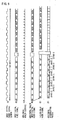
- Figure 2 is a timing chart showing a process content of a video signal;
- Figure 3 is a descriptive diagram showing a video displaying in each field;
- A portion (a) in Figure 4 is a descriptive diagram showing an input digital video signal (B) in a first field;
- A portion (b) in Figure 4 is a descriptive diagram showing an input digital video signal (B) in a second field
- Portions (c) and (d) in Figures 4 are descriptive diagrams showing displaying examples in which display phases are deviated (shifted);
- A portion (e) in Figure 4 is a descriptive diagram showing a case that dots are not deviated (shifted), for the sake of reference;
- Figure 5 is a block diagram showing a conventional display driving device (a horizontal scaler);
- Figure 6 is a timing chart showing a content of a conventional process of a video signal; and
- Figure 7 is a descriptive diagram describing a conventional video displaying in each field.
- Below, an embodiment of the present invention will be described based on Figure 1 to Figure 4.
- Figure 1 is a block diagram showing a
display driving device 10 and aliquid crystal panel 20, and Figure 2 is a simple operational description of thedisplay driving device 10. An input digital video signal (B) is synchronous with a leading edge of a clock Φ 1 (A), and is input into a D-type flip-flop 11. In this example, a horizontalscaler clock Φ 2 is produced by doubling theclock Φ 1 in adoubler 12. In addition, for the sake of simplicity, in this example, the number of horizontal dots of the input digital video signal is 640 dots, and the number of horizontal dots of the panel is 1280 dots. - A digital video signal (D) is the input digital video signal (B) as it is. A 1-clock-delay video signal (E) by the
Φ 2 is an output of the D-type flip-flop 11, and becomes a signal generated by delaying by one clock the digital video signal (B) input in thedisplay driving device 10 at timing of a leading edge of the horizontalscaler clock Φ 2. At second leading timing of the horizontalscaler clock Φ 2 in Figure 2, "A0" of the digital video signal (B) is retained and output, and then, the "A0" becomes an output of the 1-clock-delay video signal (E) by theΦ 2. At third leading timing of the horizontalscaler clock Φ 2, the digital video signal (B) has not yet become "A1", and the output of the 1-clock-delay video signal (E) by theΦ 2 is still "A0". At fourth leading timing of the horizontalscaler clock Φ 2, the output of the 1-clock-delay video signal (E) by theΦ 2 is switched to "A1", for example. Both the digital video signal (D) and the 1-clock-delay video signal (E) are to be output in a period half a Φ2 period. - A field determination (distinction)
circuit 13 inputs a horizontal synchronizing signal and a vertical synchronizing signal, and supplies to a selection circuit 14 a switching signal (in a case of a first field, a logic high signal, and in a case of a second field, a logic low signal, for example) indicating whether the first field or the second field. - The
selection circuit 14 selects the digital video signal (D) input in a terminal A in a case of the switching signal is the logic high signal, or selects the 1-clock-delay video signal (E) input in a terminal B in a case of the logic low signal, for example. - The
liquid crystal panel 20 receives theΦ 2 as an operation clock, and receives either the digital video signal (D or E) selected in theselection circuit 14. Although not shown, in a case of an enable signal is high, the selected digital video signal is sequentially shifted in a shift register of theliquid crystal panel 20. In addition, at a time that a shift of the video signal worth 1 line is completed, each data is fetched within a latch circuit by a latch pulse. At this time, if a line number selected in a gate driver line selection circuit not shown is 0 (zero), a video signal that is D/A (digital to analog)-converted is written into a line 0 (zero). Similarly, a line to be selected is sequentially shifted to 1, 2, 3, and an image is displayed on thepanel 20. - Herein, the digital video signal (D or E) is output in a period half the Φ2 period. The operation clock of the
panel 20 is theΦ 2. Thus, same dot data in the video signal (a same-location signal value in the video signal) is successively supplied to adjacent two dots aligned horizontally on theliquid crystal panel 20. - At timing of the first field in the video signal, the input digital video signal (B) in this field is supplied, without being delayed, to the
liquid crystal panel 20 as the digital video signal (D). In an example shown in Figure 3, dot data A0 is written into adjacent dots "a", "b" at the endmost of theliquid crystal panel 20, and dot data A1 is written into subsequent adjacent two dots "c", "d". On the other hand, at timing of the second field, the input digital video signal (B) in this field is delayed, and supplied to theliquid crystal panel 20 as the 1-clock-delay video signal (E). Therefore, as shown in Figure 3, there is no dot data (xx) with respect to the dot "a" in the second field, the dot data A0 is written into the adjacent dots "b", "c" of theliquid crystal panel 20, and the dot data A1 is written into the subsequent adjacent two dots "d", "e". - A video displaying example by the above-described display driving process is shown in Figure 4. A portion (a) in Figure 4 shows the input digital video signal (B) in the first field, and a portion (b) in Figure 4 shows the input digital video signal (B) in the second field. In a portion (c) in Figure 4, as a result of the above-described display driving process, a second-field video is deviated (shifted) by half the 1 clock (Φ1) to the right with respect to a first-field video. That is, a visual accumulation effect of the first-field video and the second-field video allows a user to recognize the video in the above-described portion (c) in Figure 4. It is noted that as shown in a portion (d) in Figure 4, it may be possible to carry out a process in which the second-field video is deviated (shifted) by half the 1 clock (Φ1) to the left with respect to the first-field video. In addition, for the sake of reference, the video displaying of a case that the dots are not deviated (shifted) is shown in a portion (e) in Figure 4.
- As described above, the display driving device of the present embodiment eliminates a need of the horizontal scaler in the conventional configuration. That is, a displaying phase (a writing phase) on the
panel 20 is deviated (shifted) by 180 degrees (deviated (shifted) half a period of the Φ1) by each field, without increasing the number of horizontal dots to 1280 dots by the horizontal scaler, so that it is made possible to realize a visual increase of the number of horizontal dots. Thus, the horizontal scaler is rendered unnecessary, so that a cost is reduced. In addition, it becomes possible to lower the frequency of the digital video signal to be transmitted to the display panel 20 (in the embodiment, the frequency is reduced by half compared to the prior art), which enables a data transmission to be performed, without relying on the LVDS. - It is noted that in the above-described example, there is no dot data with respect to the dot "a" in the second field. However, it may be possible to adopt a technique in which the dot data A0 in the second field is taken out from the input digital video signal (B), and the dot data A0 is supplied to the liquid
crystal display panel 20 during a period of half theΦ 2 prior to a selection output of the 1-clock-delay video signal (E) of the second field, for example. Furthermore, in the above description, it is shown an example in which the liquid crystal panel is driven. However, it is not always the case. The display driving device of the present embodiment becomes capable of improving a video quality especially when in use for driving a so-called hold-type displaying element such as the liquid crystal panel, and others. - Although the present embodiment has been described and illustrated in detail, it is clearly understood that the same is by way of illustration and example only and is not to be taken by way of limitation, the spirit and scope of the present invention encompassing at least everything falling within the terms of the appended claims.
Claims (5)
- A display driving device for applying a scale conversion to a video signal and driving a display, comprising:a means for successively supplying to a plurality of adjacent dots aligned horizontally on a display a same-location signal value of said video signal;a means for determining a first field and a second field in the video signal; anda means for deviating a writing phase of the video signal of said display depending on the first field or the second field.
- A display driving device according to claim 1, wherein by delaying one of the two fields, that is, the first field and the second field in the video signal, said writing phase is deviated.
- A display driving device according to claim 1 or 2, wherein said display is a hold-type display such as a liquid crystal panel, and others.
- A display driving device, for driving a display with a first number of dots per line to display an image according to an image signal having a second number of dots per line,
characterised in that
the display driving device is arranged to supply in turn the image data values of successive dots in the image signal to the display and to change the supplied data value at a clock frequency based on the second number of dots per line,
and in that
the display driving device is arranged to supply a write clock signal to the display at a clock frequency based on the first number of dots per line. - A display driving device according to claim 4 which is arranged to cause a horizontal offset between the image displayed in one field and the image displayed in the next field.
Applications Claiming Priority (1)
| Application Number | Priority Date | Filing Date | Title |
|---|---|---|---|
| JP2004187642A JP4646556B2 (en) | 2004-06-25 | 2004-06-25 | Display drive device |
Publications (2)
| Publication Number | Publication Date |
|---|---|
| EP1612759A2 true EP1612759A2 (en) | 2006-01-04 |
| EP1612759A3 EP1612759A3 (en) | 2009-09-30 |
Family
ID=34982604
Family Applications (1)
| Application Number | Title | Priority Date | Filing Date |
|---|---|---|---|
| EP05253872A Withdrawn EP1612759A3 (en) | 2004-06-25 | 2005-06-22 | Display driving device |
Country Status (5)
| Country | Link |
|---|---|
| US (1) | US20060001633A1 (en) |
| EP (1) | EP1612759A3 (en) |
| JP (1) | JP4646556B2 (en) |
| CN (1) | CN100449602C (en) |
| TW (1) | TW200606780A (en) |
Families Citing this family (1)
| Publication number | Priority date | Publication date | Assignee | Title |
|---|---|---|---|---|
| JP2010008598A (en) * | 2008-06-25 | 2010-01-14 | Funai Electric Co Ltd | Video display device |
Citations (2)
| Publication number | Priority date | Publication date | Assignee | Title |
|---|---|---|---|---|
| JP2002244629A (en) | 2001-01-15 | 2002-08-30 | Samsung Electronics Co Ltd | Panel driving device and panel driving system for liquid crystal display device |
| JP2003152522A (en) | 2001-08-02 | 2003-05-23 | Koninkl Philips Electronics Nv | Universal PECL / LVDS output configuration circuit |
Family Cites Families (22)
| Publication number | Priority date | Publication date | Assignee | Title |
|---|---|---|---|---|
| JP2742261B2 (en) * | 1987-12-07 | 1998-04-22 | 富士通株式会社 | Matrix type display device |
| JP2000020014A (en) * | 1998-07-06 | 2000-01-21 | Furontekku:Kk | Image display device |
| JP3529617B2 (en) * | 1998-04-07 | 2004-05-24 | アルプス電気株式会社 | Driving circuit and driving method for image display device |
| GB9012326D0 (en) * | 1990-06-01 | 1990-07-18 | Thomson Consumer Electronics | Wide screen television |
| JP2659900B2 (en) * | 1993-10-14 | 1997-09-30 | インターナショナル・ビジネス・マシーンズ・コーポレイション | Display method of image display device |
| JP3219640B2 (en) * | 1994-06-06 | 2001-10-15 | キヤノン株式会社 | Display device |
| JP2869006B2 (en) * | 1994-10-13 | 1999-03-10 | インターナショナル・ビジネス・マシーンズ・コーポレイション | Video signal processing apparatus and video signal processing method |
| JPH09204160A (en) * | 1996-01-29 | 1997-08-05 | Matsushita Electric Ind Co Ltd | Liquid crystal display |
| JP2923906B2 (en) * | 1996-06-07 | 1999-07-26 | 日本電気株式会社 | Drive circuit for liquid crystal display |
| US6380979B1 (en) * | 1996-07-02 | 2002-04-30 | Matsushita Electric Industrial Co., Ltd. | Scanning line converting circuit and interpolation coefficient generating circuit |
| JPH1069253A (en) * | 1996-08-26 | 1998-03-10 | Sanyo Electric Co Ltd | Liquid crystal display |
| WO1998040874A1 (en) * | 1997-03-10 | 1998-09-17 | Komatsu Ltd. | Image synthesizing device, image conversion device, and methods |
| JP3625145B2 (en) * | 1999-01-26 | 2005-03-02 | シャープ株式会社 | Image enlargement device |
| KR100304899B1 (en) * | 1999-07-31 | 2001-09-29 | 구자홍 | Apparatus and method for displaying out of range video of monitor |
| JP2002006790A (en) * | 2000-06-20 | 2002-01-11 | Sanyo Electric Co Ltd | Digital display signal processing circuit and digital display signal processing method |
| KR100442304B1 (en) * | 2000-07-07 | 2004-08-04 | 가부시끼가이샤 도시바 | Display method for liquid crystal display device |
| CN1162011C (en) * | 2000-11-08 | 2004-08-11 | Tcl王牌电子(深圳)有限公司 | TV set with time-share sterescopic image function |
| JP2002215082A (en) * | 2001-01-23 | 2002-07-31 | Matsushita Electric Ind Co Ltd | Image display panel and driving method thereof |
| JP2002323876A (en) * | 2001-04-24 | 2002-11-08 | Nec Corp | Image display method and liquid crystal display device in liquid crystal display device |
| JP3625195B2 (en) * | 2001-07-13 | 2005-03-02 | 日本ビクター株式会社 | Pixel number converter |
| JP4009174B2 (en) * | 2001-11-09 | 2007-11-14 | シャープ株式会社 | Liquid crystal display |
| JP2004093717A (en) * | 2002-08-30 | 2004-03-25 | Hitachi Ltd | Liquid crystal display |
-
2004
- 2004-06-25 JP JP2004187642A patent/JP4646556B2/en not_active Expired - Fee Related
-
2005
- 2005-06-22 EP EP05253872A patent/EP1612759A3/en not_active Withdrawn
- 2005-06-23 CN CNB2005100981696A patent/CN100449602C/en not_active Expired - Fee Related
- 2005-06-23 US US11/159,407 patent/US20060001633A1/en not_active Abandoned
- 2005-06-24 TW TW094121121A patent/TW200606780A/en not_active IP Right Cessation
Patent Citations (2)
| Publication number | Priority date | Publication date | Assignee | Title |
|---|---|---|---|---|
| JP2002244629A (en) | 2001-01-15 | 2002-08-30 | Samsung Electronics Co Ltd | Panel driving device and panel driving system for liquid crystal display device |
| JP2003152522A (en) | 2001-08-02 | 2003-05-23 | Koninkl Philips Electronics Nv | Universal PECL / LVDS output configuration circuit |
Also Published As
| Publication number | Publication date |
|---|---|
| JP2006011015A (en) | 2006-01-12 |
| CN1734551A (en) | 2006-02-15 |
| TW200606780A (en) | 2006-02-16 |
| JP4646556B2 (en) | 2011-03-09 |
| EP1612759A3 (en) | 2009-09-30 |
| TWI310168B (en) | 2009-05-21 |
| US20060001633A1 (en) | 2006-01-05 |
| CN100449602C (en) | 2009-01-07 |
Similar Documents
| Publication | Publication Date | Title |
|---|---|---|
| US6331862B1 (en) | Image expansion display and driver | |
| JP2001042852A (en) | Display device, method, and computer-readable storage medium | |
| US5808596A (en) | Liquid crystal display devices including averaging and delaying circuits | |
| JP3472679B2 (en) | Liquid crystal drive circuit and liquid crystal display device | |
| US7764258B2 (en) | Liquid crystal display apparatus and alternating current driving method therefore | |
| KR920010748B1 (en) | Halftone display driving circuit and halftone display method of liquid crystal matrix panel | |
| US6928118B1 (en) | Device and method for displaying video | |
| JP3602343B2 (en) | Display device | |
| US20060001633A1 (en) | Display driving device | |
| JP3751588B2 (en) | Horizontal shift clock pulse selection circuit for color LCD panel drive | |
| US20070229422A1 (en) | Method and device for controlling delta panel | |
| KR100433239B1 (en) | Apparatus and Method For Transmitting Data And Apparatus And Method for Driving Liquid Crystal Display Using The Same | |
| US8587722B1 (en) | System and method for automatically controlling the phase of a clock signal for sampling an HDTV signal | |
| KR100504077B1 (en) | Liquid crystal display apparatus for controling showing area | |
| JPH11338403A (en) | Display device | |
| JPH08171364A (en) | Liquid crystal drive | |
| EP1589514A2 (en) | Video signal processing circuit, video display, and display driving device | |
| JPH10222133A (en) | Drive circuit for liquid crystal display | |
| KR970002886Y1 (en) | A horizontal driving circuit in a lcd | |
| CN100435554C (en) | Phase recovery method and circuit for image signal processing with phase enhancement leading to weakening | |
| CN100409682C (en) | Image signal processing circuit, image display device and display drive device | |
| JP2009232014A (en) | Phase adjustment circuit | |
| JP2000267620A (en) | Flat panel display | |
| JP2006113304A (en) | Video display apparatus | |
| JPH10304282A (en) | LCD drive circuit |
Legal Events
| Date | Code | Title | Description |
|---|---|---|---|
| PUAI | Public reference made under article 153(3) epc to a published international application that has entered the european phase |
Free format text: ORIGINAL CODE: 0009012 |
|
| AK | Designated contracting states |
Kind code of ref document: A2 Designated state(s): AT BE BG CH CY CZ DE DK EE ES FI FR GB GR HU IE IS IT LI LT LU MC NL PL PT RO SE SI SK TR |
|
| AX | Request for extension of the european patent |
Extension state: AL BA HR LV MK YU |
|
| PUAL | Search report despatched |
Free format text: ORIGINAL CODE: 0009013 |
|
| AK | Designated contracting states |
Kind code of ref document: A3 Designated state(s): AT BE BG CH CY CZ DE DK EE ES FI FR GB GR HU IE IS IT LI LT LU MC NL PL PT RO SE SI SK TR |
|
| AX | Request for extension of the european patent |
Extension state: AL BA HR LV MK YU |
|
| AKX | Designation fees paid |
Designated state(s): DE FR GB |
|
| STAA | Information on the status of an ep patent application or granted ep patent |
Free format text: STATUS: THE APPLICATION IS DEEMED TO BE WITHDRAWN |
|
| 18D | Application deemed to be withdrawn |
Effective date: 20100401 |