EP1612608A2 - Positioning apparatus and photolithography apparatus including the same - Google Patents
Positioning apparatus and photolithography apparatus including the same Download PDFInfo
- Publication number
- EP1612608A2 EP1612608A2 EP05254122A EP05254122A EP1612608A2 EP 1612608 A2 EP1612608 A2 EP 1612608A2 EP 05254122 A EP05254122 A EP 05254122A EP 05254122 A EP05254122 A EP 05254122A EP 1612608 A2 EP1612608 A2 EP 1612608A2
- Authority
- EP
- European Patent Office
- Prior art keywords
- stage
- disposed
- movement stage
- light
- fine movement
- Prior art date
- Legal status (The legal status is an assumption and is not a legal conclusion. Google has not performed a legal analysis and makes no representation as to the accuracy of the status listed.)
- Withdrawn
Links
Images




Classifications
-
- G—PHYSICS
- G03—PHOTOGRAPHY; CINEMATOGRAPHY; ANALOGOUS TECHNIQUES USING WAVES OTHER THAN OPTICAL WAVES; ELECTROGRAPHY; HOLOGRAPHY
- G03F—PHOTOMECHANICAL PRODUCTION OF TEXTURED OR PATTERNED SURFACES, e.g. FOR PRINTING, FOR PROCESSING OF SEMICONDUCTOR DEVICES; MATERIALS THEREFOR; ORIGINALS THEREFOR; APPARATUS SPECIALLY ADAPTED THEREFOR
- G03F7/00—Photomechanical, e.g. photolithographic, production of textured or patterned surfaces, e.g. printing surfaces; Materials therefor, e.g. comprising photoresists; Apparatus specially adapted therefor
- G03F7/70—Microphotolithographic exposure; Apparatus therefor
- G03F7/70691—Handling of masks or workpieces
- G03F7/70775—Position control, e.g. interferometers or encoders for determining the stage position
-
- G—PHYSICS
- G01—MEASURING; TESTING
- G01B—MEASURING LENGTH, THICKNESS OR SIMILAR LINEAR DIMENSIONS; MEASURING ANGLES; MEASURING AREAS; MEASURING IRREGULARITIES OF SURFACES OR CONTOURS
- G01B11/00—Measuring arrangements characterised by the use of optical techniques
- G01B11/24—Measuring arrangements characterised by the use of optical techniques for measuring contours or curvatures
- G01B11/2441—Measuring arrangements characterised by the use of optical techniques for measuring contours or curvatures using interferometry
-
- G—PHYSICS
- G03—PHOTOGRAPHY; CINEMATOGRAPHY; ANALOGOUS TECHNIQUES USING WAVES OTHER THAN OPTICAL WAVES; ELECTROGRAPHY; HOLOGRAPHY
- G03F—PHOTOMECHANICAL PRODUCTION OF TEXTURED OR PATTERNED SURFACES, e.g. FOR PRINTING, FOR PROCESSING OF SEMICONDUCTOR DEVICES; MATERIALS THEREFOR; ORIGINALS THEREFOR; APPARATUS SPECIALLY ADAPTED THEREFOR
- G03F7/00—Photomechanical, e.g. photolithographic, production of textured or patterned surfaces, e.g. printing surfaces; Materials therefor, e.g. comprising photoresists; Apparatus specially adapted therefor
- G03F7/70—Microphotolithographic exposure; Apparatus therefor
- G03F7/70691—Handling of masks or workpieces
- G03F7/70716—Stages
-
- G—PHYSICS
- G03—PHOTOGRAPHY; CINEMATOGRAPHY; ANALOGOUS TECHNIQUES USING WAVES OTHER THAN OPTICAL WAVES; ELECTROGRAPHY; HOLOGRAPHY
- G03F—PHOTOMECHANICAL PRODUCTION OF TEXTURED OR PATTERNED SURFACES, e.g. FOR PRINTING, FOR PROCESSING OF SEMICONDUCTOR DEVICES; MATERIALS THEREFOR; ORIGINALS THEREFOR; APPARATUS SPECIALLY ADAPTED THEREFOR
- G03F7/00—Photomechanical, e.g. photolithographic, production of textured or patterned surfaces, e.g. printing surfaces; Materials therefor, e.g. comprising photoresists; Apparatus specially adapted therefor
- G03F7/70—Microphotolithographic exposure; Apparatus therefor
- G03F7/708—Construction of apparatus, e.g. environment aspects, hygiene aspects or materials
- G03F7/7085—Detection arrangement, e.g. detectors of apparatus alignment possibly mounted on wafers, exposure dose, photo-cleaning flux, stray light, thermal load
-
- G—PHYSICS
- G03—PHOTOGRAPHY; CINEMATOGRAPHY; ANALOGOUS TECHNIQUES USING WAVES OTHER THAN OPTICAL WAVES; ELECTROGRAPHY; HOLOGRAPHY
- G03F—PHOTOMECHANICAL PRODUCTION OF TEXTURED OR PATTERNED SURFACES, e.g. FOR PRINTING, FOR PROCESSING OF SEMICONDUCTOR DEVICES; MATERIALS THEREFOR; ORIGINALS THEREFOR; APPARATUS SPECIALLY ADAPTED THEREFOR
- G03F9/00—Registration or positioning of originals, masks, frames, photographic sheets or textured or patterned surfaces, e.g. automatically
- G03F9/70—Registration or positioning of originals, masks, frames, photographic sheets or textured or patterned surfaces, e.g. automatically for microlithography
- G03F9/7003—Alignment type or strategy, e.g. leveling, global alignment
- G03F9/7023—Aligning or positioning in direction perpendicular to substrate surface
- G03F9/7026—Focusing
-
- G—PHYSICS
- G03—PHOTOGRAPHY; CINEMATOGRAPHY; ANALOGOUS TECHNIQUES USING WAVES OTHER THAN OPTICAL WAVES; ELECTROGRAPHY; HOLOGRAPHY
- G03F—PHOTOMECHANICAL PRODUCTION OF TEXTURED OR PATTERNED SURFACES, e.g. FOR PRINTING, FOR PROCESSING OF SEMICONDUCTOR DEVICES; MATERIALS THEREFOR; ORIGINALS THEREFOR; APPARATUS SPECIALLY ADAPTED THEREFOR
- G03F9/00—Registration or positioning of originals, masks, frames, photographic sheets or textured or patterned surfaces, e.g. automatically
- G03F9/70—Registration or positioning of originals, masks, frames, photographic sheets or textured or patterned surfaces, e.g. automatically for microlithography
- G03F9/7003—Alignment type or strategy, e.g. leveling, global alignment
- G03F9/7023—Aligning or positioning in direction perpendicular to substrate surface
- G03F9/703—Gap setting, e.g. in proximity printer
-
- H—ELECTRICITY
- H10—SEMICONDUCTOR DEVICES; ELECTRIC SOLID-STATE DEVICES NOT OTHERWISE PROVIDED FOR
- H10P—GENERIC PROCESSES OR APPARATUS FOR THE MANUFACTURE OR TREATMENT OF DEVICES COVERED BY CLASS H10
- H10P72/00—Handling or holding of wafers, substrates or devices during manufacture or treatment thereof
- H10P72/06—Apparatus for monitoring, sorting, marking, testing or measuring
- H10P72/0606—Position monitoring, e.g. misposition detection or presence detection
Definitions
- the coarse movement stage 2 is driven by a linear motor.
- Linear motor fixing parts 17X and 17Y are disposed on the base 5.
- a linear motor moving part 18X moves in the X direction relative to the linear motor fixing part 17X
- a linear motor moving part 18Y moves in the Y direction relative to the linear motor fixing part 17Y.
- the linear motor moving parts 18X and 18Y penetrate the coarse movement stage 2. As the linear motor moving parts 18X and 18Y move, the coarse movement stage 2 moves in the X and Y direction within a large area.
- a projection optical system 20 and an alignment optical system 30 are supported by a supporting member 4.
- the base guiding the coarse movement stages 21 and 22 is divided into an exposure area 52 and a measurement area 51.
- the exposure area 52 is an area below the projection optical system 20 in which the coarse and fine movement stages are moved on the base when exposing the wafer disposed on the fine movement stage 11 and 12.
- the measurement area 51 is the area below the alignment optical system 30 in which the coarse and fine movement stages are moved on the base when aligning the wafers disposed on the fine movement stages 11 and 12.
- Mirrors 16a and 16b having XY planes (reflective planes disposed orthogonally to the vertical direction) are disposed on the supporting member 4.
- the mirrors 16a and 16b are interposed between the exposure area 52 and the measurement area 51.
- Z interferometers 15a and 15b are disposed so that they emit measurement light beams and reference light beams in both directions along the X axis below the mirrors 16a and 16b.
Landscapes
- Physics & Mathematics (AREA)
- General Physics & Mathematics (AREA)
- Health & Medical Sciences (AREA)
- Engineering & Computer Science (AREA)
- Environmental & Geological Engineering (AREA)
- Epidemiology (AREA)
- Public Health (AREA)
- Exposure And Positioning Against Photoresist Photosensitive Materials (AREA)
- Exposure Of Semiconductors, Excluding Electron Or Ion Beam Exposure (AREA)
Abstract
Description
- The present invention relates to a positioning apparatus and, more specifically, relates to a positioning apparatus included in a photolithography apparatus used for producing devices such as semiconductors and liquid crystal devices.
- When using a photolithography apparatus for producing a device such as a semiconductor or a liquid crystal device, the substrate must be positioned highly accurately. A positioning mechanism for the photolithography apparatus may include a coarse movement stage movable in a large area and a fine movement stage movable in a smaller area as compared to the coarse movement stage.
- Japanese Patent Laid-Open No. 2001-143997 discloses a method for measuring the displacement of a fine movement stage, on which a wafer is disposed, in the Z direction (vertical direction) for a photolithography apparatus. This method will be briefly described with reference to Fig. 6.
- The positioning apparatus illustrated in Fig. 6 includes a coarse movement stage Sc and a fine movement stage Sf. An X-direction moving element Mx of the coarse movement stage Sc is movable in the X and Y directions relative to a stage base Bs. The fine movement stage Sf is disposed on the X-direction moving element Mx and is movable in a smaller area relative to the X-direction moving element Mx.
- An instrument base Bi is provided for mounting components on the measurement reference side of the positioning apparatus. The instrument base Bi includes an
X interferometer 11 for measuring the position of the fine movement stage Sf in the X direction and aZ interferometer 12 for measuring the position of the fine movement stage Sf in the Z direction. - A mirror surface (light reflector) p1 for measuring the position in the X direction and a
bar mirror 54 and a mirror surface p2 for measuring the position in the Z direction are disposed on the fine movement stage Sf. A mirror surface p7 for measuring the position in the Z direction is disposed on the instrument base Bi. - A measurement light beam emitted from the
Z interferometer 12 is reflected at the mirror surfaces p2 and p7 and is returned to theZ interferometer 12. The measurement light beam is interfered with a reference light beam (not shown in the drawing) to measure a displacement dx+dz. A measurement light beam emitted from theX interferometer 11 is reflected at the mirror surface p1 and returned to theX interferometer 11. The measurement light beam is interfered with a reference light beam (not shown in the drawing) to measure a displacement dx. The displacement in the Z direction is measured by obtaining the difference between the displacement dx+dz and the displacement dx. - In the above-described structure, the reference light beam is guided for a predetermined distance. Therefore, if there is a temperature difference between the light paths of the measurement light beam and the reference light beam, an error occurs in the measured value. In particular, when determining the displacement in the Z direction using the X and
Z interferometers Z interferometers Z interferometers - It is undesirable to dispose a mirror having a reflective surface at an acute angle relative to the vertical direction, such as the
bar mirror 54, as illustrated in Fig. 6, on the fine movement stage Sf because it will have negative effects on the weight and rigidity of the fine movement stage Sf and will cause a degradation in the control of the fine movement stage Sf. - The present invention is directed to a positioning apparatus. In one aspect of the present invention, a positioning apparatus includes a first stage, a second stage movable relative to the first stage, a pair of first light reflectors disposed on the first stage, the first light reflectors positioned at an acute angle with respect to a vertical axis of the apparatus, a pair of second light reflectors disposed on the second stage, the second light reflectors positioned orthogonal to the vertical axis, a reference structure facilitating measurement of a vertical position of the second stage, a pair of third light reflectors disposed on the reference structure, the third light reflectors positioned orthogonal to the vertical axis, and a pair of interferometers configured to measure the vertical position of the second stage using light reflected, in use, from the first, second, and third light reflectors.
- The positioning apparatus according to the present invention is capable of reducing errors in the measurement of the vertical direction. As a result, a second stage of the positioning apparatus can be positioned highly accurately.
- Further features and advantages of the present invention will become apparent from the following description of exemplary embodiments (with reference to the attached drawings).
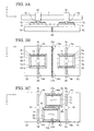
- Figs. 1A-C are schematic drawings illustrating a positioning apparatus according to a first embodiment of the present invention.
- Figs. 2A and 2B are schematic drawings illustrating a positioning apparatus according to a variation of the first embodiment of the present invention.
- Figs. 3A-C are schematic drawings illustrating a positioning apparatus according to a second embodiment of the present invention.
- Fig. 4 is a schematic drawing illustrating a process for producing a device.
- Fig. 5 is a schematic drawing illustrating a process for producing a wafer.
- Fig. 6 is a schematic drawing illustrating a known positioning apparatus.
- A positioning apparatus according to a first embodiment of the present invention will now be described. In this embodiment, a photolithography apparatus including the positioning apparatus is described. The photolithography apparatus is used for manufacturing semiconductor devices, such as semiconductor integrated circuits, and devices having fine patterns, such as micromachines and thin film magnetic heads. By emitting an exposure light beam as exposure energy from a
lighting system 50 to a wafer, which is a substrate, via areticle 40, which is the original plate, and via a projection lens, which is aprojection lens system 20, a predetermined pattern is formed on the wafer disposed on the positioning apparatus. Here, the term "exposure light beam" is a generic term referring to one of a visible light beam, an ultraviolet light beam, an extreme ultraviolet (EUV) light beam, an X-ray beam, an electron beam, and a charged particle beam. The term "projection lens" is a generic term referring to one of a refractive lens, a reflective lens, a catadioptric lens, and a charged particle lens. The pattern may be transferred using a step-and-repeat method or a step-and-scan method. - As illustrated in Fig. 1A, the positioning apparatus includes a
coarse movement stage 2, that moves in a large area relative to abase 5, and afine movement stage 1 that is disposed on thecoarse movement stage 2 and moves in a small area relative to thecoarse movement stage 2. A wafer is disposed on thefine movement stage 1 and is highly accurately positioned relative to the pattern. - The
coarse movement stage 2 is supported movably in the X and Y directions relative to thebase 5. As a support mechanism, air bearings may be used to float thecoarse movement stage 2 or a magnetic force, such as magnetic attraction or a Lorentz force, may be utilized to float thecoarse movement stage 2. Thecoarse movement stage 2 is floated to improve accuracy. According to this embodiment, a surface motor is used as a driving mechanism. In general, the surface motor generates a driving force by applying an electric current to a coil connected to a moving element (movement stage 2) or a fixed element (base 5). The method for generating a driving force may be a system based on variable magnetic resistance (surface pulse motor) or a system based on Lorentz force. Since the mechanisms of these system are disclosed in Japanese Patent Laid-Open Nos. 11-190786 (corresponding to U.S. Patent No. 6,414,742) and 2003-123832 (corresponding to U.S. Patent No. 6,664,619), detailed descriptions are omitted in this document. - The
fine movement stage 1 moves in large strokes together with thecoarse movement stage 2 in the X and Y directions by, for example, electromagnetic coupling. Anactuator 3 is interposed between thecoarse movement stage 2 and thefine movement stage 1. Theactuator 3 moves thefine movement stage 1 in a small area relative to thecoarse movement stage 2. Theactuator 3 may be a linear motor, an electromagnet, an air actuator, or a piezoelectric element. Better accuracy can be achieved by using a non-contact actuator. - The
fine movement stage 1 may be driven in six directions: along the X axis, along the Y axis, along the Z axis (vertical axis), in the ωx direction (around the X axis), in the ωy direction (around the Y axis), and in the ωx direction (around the X axis). However, the number of driving directions is not limited to six directions. - A supporting
member 4 is a reference structure that functions as a reference for measuring the position of thefine movement stage 1. The supportingmember 4 according to this embodiment supports the projectionoptical system 20. In other words, if a structure other than the supporting member is used as a reference for measuring the position of thefine movement stage 1, the structure will be equivalent to the supportingmember 4 according to this embodiment. - Next, the position measurement by the positioning apparatus according to this embodiment will be described with reference to Fig. 1B. Fig. 1B is an exploded view of Fig. 1A. An
X interferometer 10 for measuring the position of thefine movement stage 1 in the X direction, a Y interferometer (not shown in the drawing), andZ interferometers fine movement stage 1 in the Z direction are disposed on the supportingmember 4. - Mirrors (light reflectors) 6a and 6b are disposed on the
coarse movement stage 2. The reflective surfaces of themirrors mirrors Z interferometers mirrors coarse movement stage 2 or may be provided as a unit with thecoarse movement stage 2. -
Mirrors fine movement stage 1. Any type of component may be used as themirrors mirrors - Similarly, mirrors 8a and 8b having XY planes (reflective surfaces orthogonal to the vertical direction) are disposed on the supporting
member 4. Any type of component may be used as themirrors mirrors - The
Z interferometer 9a (9b) measures displacement by emitting a reference light beam La and a measurement light beam Lb and measuring the interference of the two light beams when reflected back. The dotted lines in Fig. 1B indicate light paths of the reference light beam La and the measurement light beam Lb. The reference light beam La and the measurement light beam Lb emitted from theZ interferometer 9a (9b) are bent in the Z direction at themirror 6a (6b). By emitting the reference light beam La and the measurement light beam Lb at different positions on the reflective surface of themirror 6a (6b), the reference light beam La is reflected to themirror 7a (7b) and the measurement light beam Lb is reflected to themirror 8a (8b). The reference light beam La and the measurement light beam Lb emitted to themirrors 7a (7b) and 8a (8b), respectively, in the +Z direction is reflected back in the -Z direction. The reflected light beams La and Lb are bent again at themirror 6a (6b) and returned to theZ interferometer 9a (9b). The interference between the reference light beam La and the measurement light beam Lb enables theZ interferometer 9a - The horizontal (X direction in the drawing) portion dx of the light paths of the reference light beam La and the measurement light beam Lb, pass through substantially the same space, and therefore, the effect of the air fluctuation is cancelled out. Accordingly, errors in the measurement are reduced.
- Here, the reference light beam La may be used as a measurement light beam, and the measurement light beam Lb may be used as a reference light beam, so long as the difference between the two light beams are determined by interfering the two light beams.
- The measurement light beam Lb from the
X interferometer 10 is reflected at the side surface (YZ plane) of themirror 7a (7b) and enters theX interferometer 10 again. TheX interferometer 10 measures the position of thefine movement stage 1 in the X direction from the difference between the measurement light beam Lb and a reference light beam not shown in the drawing. The mirrors for measuring the position of thefine movement stage 1 in the X and Z directions are provided separately in this embodiment. Alternatively, the same mirrors may be used for measuring the position of thefine movement stage 1 in each direction. - For measuring the position of the
fine movement stage 1 in the Y direction, a mirror having an XZ plane is disposed on thefine movement stage 1. A measurement light beam is emitted from the Y interferometer (not shown in the drawing) is reflected at the mirror and a measurement can be made in the same manner as the measurement in the X direction. - By disposing a plurality of X and Y interferometers, the rotational directions (ωx, ωy, ωy directions) of the
fine movement stage 1 can be measured. - Fig. 1C illustrates the positioning apparatus according to this embodiment viewed from the +Z direction. As illustrated in the drawing, the
mirrors Z interferometers fine movement stage 1 is moved. - The
mirrors coarse movement stage 2, and themirrors fine movement stage 1. In this way, even when the projectionoptical system 20 is disposed above the mirror on one side (for example, mirrors 6a and 7a), the mirrors on the other side (for example, mirrors 6b and 7b) can be used to measure the position of thefine movement stage 1 in the Z direction. In other words, even when thecoarse movement stage 2 is moved within a large area, at least one of theZ interferometers fine movement stage 1 in the Z direction. Accordingly, the position of thefine movement stage 1 in the Z direction can always be measured. - According to the above-described structure, the reflective surfaces of the
mirrors member 4. Themirrors mirrors mirrors mirrors optical system 20 along a straight line passing through the projectionoptical system 20. In this way, the size of the mirrors, which are components that require accuracy, can be reduced to improve accuracy and reduce production cost of the positioning apparatus. - The measurement light beam Lb from the
Z interferometer 9a (9b) is guided in the X direction such that the measurement light beam Lb is emitted at themirror 6a (6b) below themirror 8a (8b). - The
mirror 6a (6b) and themirror 7a (7b) may be disposed along the X axis and themirror 8a (8b) may be disposed along the Y axis so that theZ interferometer 9a (9b) emits light beams along the Y axis to themirror 6a (6b). - In the description above, the
coarse movement stage 2 is driven by a surface motor. However, the driving force is not limited to a surface motor and various driving mechanisms may by used to drive thecoarse movement stage 2. - According to a variation of the first embodiment, as illustrated in Fig. 2, the
coarse movement stage 2 is driven by a linear motor. Linearmotor fixing parts base 5. A linearmotor moving part 18X moves in the X direction relative to the linearmotor fixing part 17X, and a linearmotor moving part 18Y moves in the Y direction relative to the linearmotor fixing part 17Y. The linearmotor moving parts coarse movement stage 2. As the linearmotor moving parts coarse movement stage 2 moves in the X and Y direction within a large area. - The positioning apparatus according to this embodiment is used for a photolithography apparatus. However, the positioning apparatus may be used for other apparatuses as well.
- A positioning apparatus according to a second embodiment of the present invention will now be described with reference to Fig. 3. A case in which the positioning apparatus according to this embodiment is used for a photolithography apparatus will be described. Components having the same functions as the components according to the first embodiment are indicated by the same reference numerals in the drawings and their detailed descriptions are omitted.
- The second embodiment differs from the first embodiment in that two of each coarse movement stages 21 and 22 and fine movement stages 11 and 12 (hereinafter, the pair of the coarse movement stages 21 (22) and the fine movement stages 11 (12) is referred to as "a coarse and fine movement stage") are provided. Such a positioning apparatus has been attracting attention recently for use in photolithography apparatuses. While a wafer disposed on one of the coarse and fine movement stages is being exposed, another wafer disposed on the other coarse and fine movement stage can be aligned. Therefore, throughput is improved. Here, the alignment includes aligning each chip of the wafers in the X and Y directions and also aligning the Z direction of the chips.
- In Figs. 3A-C, a projection
optical system 20 and an alignmentoptical system 30 are supported by a supportingmember 4. The base guiding the coarse movement stages 21 and 22 is divided into anexposure area 52 and ameasurement area 51. Theexposure area 52 is an area below the projectionoptical system 20 in which the coarse and fine movement stages are moved on the base when exposing the wafer disposed on thefine movement stage measurement area 51 is the area below the alignmentoptical system 30 in which the coarse and fine movement stages are moved on the base when aligning the wafers disposed on the fine movement stages 11 and 12. -
Mirrors coarse movement stage 21, and mirrors 6c and 6d are disposed on thecoarse movement stage 22.Mirrors fine movement stage 11, and mirrors 7c and 7d are disposed on thefine movement stage 12.Mirrors 8a to 8d are disposed in a direction orthogonal to a straight line connecting the projectionoptical system 20 and the alignmentoptical system 30. In other words, themirrors 8a to 8d are disposed along the X direction in the drawing. Themirrors optical system 20, and themirror optical system 30. - By disposing the
mirrors 8a to 8d in a direction orthogonal to a straight line connecting the projectionoptical system 20 and the alignmentoptical system 30, the measurement light beams and the reference light beams used to measure the position in the Z direction during exposure or measurement will not be blocked by the coarse and fine movement stages. - The functions of the
mirrors 6a to 6d, 7a to 7d, and 8a to 8d are the same as the mirrors according to the first embodiment. Therefore, descriptions are omitted. - The transposition of the two coarse and fine movement stages between the
exposure area 52 and themeasurement area 51 is described with reference to Fig. 3C. After completing the exposure of a wafer disposed on the coarse and fine movement stage (11 and 21) in theexposure area 52, the coarse and fine movement stage (11 and 21) moves to a delivery position, not shown in the drawing, to send out the exposed wafer and receive a new wafer. Then the coarse and fine movement stage (11 and 21) moves to themeasurement area 51 for alignment. The other coarse and fine movement stage (12 and 22) moves to theexposure area 52 to expose the wafer that has been aligned. These movements are repeated to align and expose a plurality of wafers. -
Mirrors member 4. Themirrors exposure area 52 and themeasurement area 51.Z interferometers mirrors - The measurement light beam and the reference light beam emitted from the
Z interferometer 15a (15b) are bent in the Z direction by themirror 6a (6d) when the two coarse and fine stages are transposed, as illustrated in Fig. 3C. By emitting the measurement light beam and reference light beam on different positions on the reflective surface of themirror 6a (6d), the reference light beam is projected onto themirror 7a (7d) and the measurement light beam is projected onto themirror 16a (16b). The measurement light beam and the reference light beam emitted in the +Z direction by themirror 7a (7d) and themirror 16a (16d) are reflected in the -Z direction, are bent at themirror 6a (6d) again, and enter theZ interferometer 15a (15b). The displacement in the Z direction between the fine movement stage 11 (21) and the supportingmember 4 is measured by making the reference light beam and the measurement light beam interfere with each other. - The horizontal (X direction in the drawing) portion dx of the light paths of the reference light beam La and the measurement light beam Lb, pass through substantially the same space, and therefore, the effect of the air fluctuation is cancelled out. Accordingly, errors in the measurement are reduced.
- By making the length of each of the
mirrors 6a to 6d and themirrors mirror Z interferometer mirror Z interferometer 15a (15b) in the Y direction, the positions of the fine movement stages 11 and 12 in the Z direction can be measured continuously. - As described above, by disposing the
mirrors exposure area 52 and themeasurement area 51, the position in the Z direction can be continuously measured even when the two coarse and fine stages are transposed. - Since the base according to this embodiment is divided into the
exposure area 52 and themeasurement area 51, the effects of the heat and oscillation in each area can be blocked and interference between the two areas can be reduced. When using a base having such a two-area structure, it is important to compensate for the Z direction of the stages when they are transposed. Therefore, a positioning apparatus such as the positioning apparatus according to this embodiment can be used. - The positioning apparatuses according to the first and the second embodiments may be used as a wafer stage of a photolithography apparatus to provide a photolithography apparatus having high accuracy and high throughput. A method for producing a device using such a photolithography apparatus will be described below.
- Next, the process for producing a semiconductor device using the above-mentioned photolithography apparatus will be described. Fig. 4 is a flow chart illustrating the overall process for producing a semiconductor device. In Step S1 (circuit design), the circuit of the semiconductor device is designed. In Step S2 (mask preparation), a mask is prepared based on the designed circuit pattern.
- In Step S3 (wafer production), a wafer is produced using a material such as silicon. Step S4 (wafer processing) is the front-end of wafer processing. In Step S4, the circuit is formed on the wafer with the mask using the photolithography apparatus. The subsequent Step S5 is the post-processing of wafer processing. In Step S5, the produced wafer is prepared into semiconductor chips. The post-processing in Step S5 includes steps such as, an assembling step (dicing and bonding) and a packaging step (chip packaging). In Step S6 (inspection), inspections, such as an operation check and a durability test, are carried out on the semiconductor device produced in Step S5. Through such steps, the production of a semiconductor device is completed, and then in Step S7, the semiconductor device is shipped.
- The wafer processing in Step S4 includes the following steps (refer to Fig. 5): an oxidation step for oxidizing the surface of the wafer, a chemical vapor deposition (CVD) step for forming an insulation film on the surface of the wafer, an electrode formation step for forming electrodes on the wafer by deposition, an ion implantation step for implanting ions into the wafer, a resist processing step for applying a photosensitizer on the wafer, an exposure step for transferring the circuit pattern onto the wafer after being processed in the resist processing step by the above-mentioned photolithography apparatus, a developing step for developing the wafer exposed in the exposure step, an etching step for removing parts other than the resist image developed in the developing step, and a resist removal step for removing the unwanted resist that has been etched. By repeating these steps, multiple circuit patterns can be formed on the wafer.
- By producing a device using the photolithography apparatus including the positioning apparatus according to the first or second embodiments as a wafer stage, fine devices can be produced at low cost.
- While the present invention has been described with reference to exemplary embodiments, it is to be understood that the invention is not limited to the disclosed embodiments. On the contrary, the invention is intended to cover various modifications and equivalent arrangements included within the spirit and scope of the appended claims. The scope of the following claims is to be accorded the broadest interpretation so as to encompass all such modifications and equivalent structures and functions.
Claims (11)
- A positioning apparatus comprising:a first stage;a second stage movable relative to the first stage;a pair of first light reflectors disposed on the first stage, the first light reflectors positioned at an acute angle with respect to a vertical axis of the apparatus;a pair of second light reflectors disposed on the second stage, the second light reflectors positioned orthogonal to the vertical axis;a reference structure facilitating measurement of a vertical position of the second stage;a pair of third light reflectors disposed on the reference structure, the third light reflectors positioned orthogonal to the vertical axis; anda pair of interferometers configured to measure the vertical position of the second stage using light reflected, in use, from the first, second, and third light reflectors.
- The positioning apparatus according to Claim 1,
wherein the first and second light reflectors extend in a first direction orthogonal to a direction in which a measurement light beam is emitted towards the first light reflectors from the interferometers. - The positioning apparatus according to Claim 2,
wherein the third light reflectors extend in a second direction orthogonal to the first direction. - The positioning apparatus according to Claim 3,
wherein the first light reflectors are disposed at opposite ends of the first stage and the second light reflectors are disposed at opposite ends of the second stage. - A photolithography apparatus for processing a substrate, comprising:a light source; andthe positioning apparatus according to any of Claims 1 to 4, the positioning apparatus configured to position the substrate relative to the light source in order to transfer a pattern onto the substrate.
- A photolithography apparatus for processing first and second substrates, comprising:two of the positioning apparatuses claimed in any of Claims 1 to 4;a projection optical system configured to expose the first substrate disposed on the second stage of one of the positioning apparatuses; andan alignment optical system configured to align the second substrate disposed on the second stage of the other of the two positioning apparatuses while the first substrate is being exposed by the projection optical system,wherein the third light reflectors of the two positioning apparatuses extend along a direction orthogonal to a line connecting the projection optical system and the alignment optical system.
- The photolithography apparatus according to Claim 6,
wherein the two positioning apparatuses are transposable between a position below the projection optical system and a position below the alignment optical system, and
wherein a pair of fourth light reflectors orthogonal to the vertical axis is disposed on the reference structure where the two positioning apparatuses pass each other when being transposed. - The photolithography apparatus according to Claim 7, further comprising a base configured to guide each first stage of the two positioning apparatus, the base defining an exposure area below the projection optical system and a measurement area below the alignment optical system.
- A photolithography apparatus comprising:a projection optical system;a supporting member arranged to support the projection optical system;a fine movement stage arranged to receive a substrate;a coarse movement stage arranged to support the fine movement stage;an interferometer arranged to emit first and second light beams in order to measure a position of the fine movement stage;a first reflective unit arranged to reflect the first and second light beams in a vertical direction, the first reflective unit being disposed on the coarse movement stage;a second reflective unit arranged to reflect the first light beam reflected by the first reflecting unit, the second reflective unit being disposed on the fine movement stage; anda third reflective unit arranged to reflect the second light beam reflected by the first reflective unit, the third reflective unit being disposed on the supporting member.
- A method for manufacturing a semiconductor device comprising the following steps:processing a wafer using the photolithography apparatus according to Claim 5; andassembling the wafer processed in the processing step into the device.
- A positioning apparatus comprising:a fine movement stage arranged to receive, in use, a substrate;a coarse movement stage arranged to support the fine movement stage;a reference structure facilitating measurement of a position of the fine movement stage in a first direction;an interferometer arranged to emit first and second light beams in order to measure a position of the fine movement stage in the first direction;a first reflective unit arranged to reflect the first and second light beams in the first direction, the first reflective unit being disposed on the coarse movement stage;a second reflective unit arranged to reflect the first light beam reflected by the first reflecting unit, the second reflective unit being disposed on the fine movement stage; anda third reflective unit arranged to reflect the second light beam reflected by the first reflective unit, the third reflective unit being disposed on the reference structure.
Applications Claiming Priority (1)
| Application Number | Priority Date | Filing Date | Title |
|---|---|---|---|
| JP2004196455A JP4262153B2 (en) | 2004-07-02 | 2004-07-02 | Positioning apparatus and exposure apparatus using the same |
Publications (2)
| Publication Number | Publication Date |
|---|---|
| EP1612608A2 true EP1612608A2 (en) | 2006-01-04 |
| EP1612608A3 EP1612608A3 (en) | 2007-10-31 |
Family
ID=34941792
Family Applications (1)
| Application Number | Title | Priority Date | Filing Date |
|---|---|---|---|
| EP05254122A Withdrawn EP1612608A3 (en) | 2004-07-02 | 2005-06-30 | Positioning apparatus and photolithography apparatus including the same |
Country Status (4)
| Country | Link |
|---|---|
| US (1) | US7193723B2 (en) |
| EP (1) | EP1612608A3 (en) |
| JP (1) | JP4262153B2 (en) |
| KR (1) | KR100658572B1 (en) |
Cited By (1)
| Publication number | Priority date | Publication date | Assignee | Title |
|---|---|---|---|---|
| CN112113509A (en) * | 2019-06-20 | 2020-12-22 | 上海微电子装备(集团)股份有限公司 | Gantry measuring device and gantry measuring method |
Families Citing this family (4)
| Publication number | Priority date | Publication date | Assignee | Title |
|---|---|---|---|---|
| DE102009025977A1 (en) | 2009-06-16 | 2010-12-23 | Q-Cells Se | Solar cell and manufacturing process of a solar cell |
| DE102011006055A1 (en) * | 2011-03-24 | 2012-09-27 | Carl Zeiss Smt Gmbh | Position measuring device for mask inspection device for inspecting lithographic mask of arrangement of a positioning system, is configured by location or tilted position or certain position of object |
| CN102998913B (en) * | 2012-12-27 | 2015-02-04 | 苏州大学 | Simultaneous localization photoetching exposure device and method |
| CN103309177B (en) * | 2013-06-19 | 2015-02-11 | 清华大学 | Workpiece platform system of photoetching machine |
Citations (1)
| Publication number | Priority date | Publication date | Assignee | Title |
|---|---|---|---|---|
| US6741358B1 (en) | 1999-09-20 | 2004-05-25 | Nikon Corporation | Exposure apparatus and device production method in which position of reference plate provided on substrate stage is measured |
Family Cites Families (9)
| Publication number | Priority date | Publication date | Assignee | Title |
|---|---|---|---|---|
| JP3531894B2 (en) * | 1996-09-13 | 2004-05-31 | キヤノン株式会社 | Projection exposure equipment |
| US6020964A (en) * | 1997-12-02 | 2000-02-01 | Asm Lithography B.V. | Interferometer system and lithograph apparatus including an interferometer system |
| JP3630964B2 (en) | 1997-12-26 | 2005-03-23 | キヤノン株式会社 | Stage apparatus, exposure apparatus using the same, and device manufacturing method |
| JP2000049066A (en) * | 1998-07-27 | 2000-02-18 | Canon Inc | Exposure apparatus and device manufacturing method |
| US6160628A (en) * | 1999-06-29 | 2000-12-12 | Nikon Corporation | Interferometer system and method for lens column alignment |
| JP2001143997A (en) | 1999-11-15 | 2001-05-25 | Canon Inc | Positioning apparatus, exposure apparatus, and device manufacturing method |
| JP3762307B2 (en) * | 2001-02-15 | 2006-04-05 | キヤノン株式会社 | Exposure apparatus including laser interferometer system |
| JP2003123832A (en) * | 2001-10-11 | 2003-04-25 | Nec Tokin Corp | Laminated film exterior power storage device and method of manufacturing the same |
| US7443511B2 (en) * | 2003-11-25 | 2008-10-28 | Asml Netherlands B.V. | Integrated plane mirror and differential plane mirror interferometer system |
-
2004
- 2004-07-02 JP JP2004196455A patent/JP4262153B2/en not_active Expired - Fee Related
-
2005
- 2005-06-21 US US11/157,781 patent/US7193723B2/en not_active Expired - Fee Related
- 2005-06-30 EP EP05254122A patent/EP1612608A3/en not_active Withdrawn
- 2005-07-01 KR KR1020050058982A patent/KR100658572B1/en not_active Expired - Fee Related
Patent Citations (1)
| Publication number | Priority date | Publication date | Assignee | Title |
|---|---|---|---|---|
| US6741358B1 (en) | 1999-09-20 | 2004-05-25 | Nikon Corporation | Exposure apparatus and device production method in which position of reference plate provided on substrate stage is measured |
Cited By (2)
| Publication number | Priority date | Publication date | Assignee | Title |
|---|---|---|---|---|
| CN112113509A (en) * | 2019-06-20 | 2020-12-22 | 上海微电子装备(集团)股份有限公司 | Gantry measuring device and gantry measuring method |
| CN112113509B (en) * | 2019-06-20 | 2022-06-17 | 上海微电子装备(集团)股份有限公司 | Gantry measuring device and gantry measuring method |
Also Published As
| Publication number | Publication date |
|---|---|
| KR100658572B1 (en) | 2006-12-19 |
| EP1612608A3 (en) | 2007-10-31 |
| JP4262153B2 (en) | 2009-05-13 |
| JP2006019549A (en) | 2006-01-19 |
| US7193723B2 (en) | 2007-03-20 |
| US20060001889A1 (en) | 2006-01-05 |
| KR20060049732A (en) | 2006-05-19 |
Similar Documents
| Publication | Publication Date | Title |
|---|---|---|
| JP6566389B2 (en) | Exposure apparatus, exposure method, and device manufacturing method | |
| JP6575829B2 (en) | Exposure apparatus, exposure method, and device manufacturing method | |
| JP4468980B2 (en) | Lithographic projection apparatus and device manufacturing method | |
| US20080174755A1 (en) | Movable Stage Apparatus | |
| TWI476540B (en) | Microlithography device and component manufacturing method | |
| JPWO2009084199A1 (en) | Exposure apparatus, exposure method, and device manufacturing method | |
| JP5455166B2 (en) | Exposure method, exposure apparatus, and device manufacturing method | |
| US20090097009A1 (en) | Holding device and exposure apparatus | |
| US7193723B2 (en) | Positioning apparatus and photolithography apparatus including the same | |
| US7738114B2 (en) | Exposure apparatus configured to minimize effects of mechanism for measuring stage position on peripheral mechanism and device-manufacturing method | |
| US20040145751A1 (en) | Square wafer chuck with mirror | |
| JP5757397B2 (en) | Exposure method, exposure apparatus, and device manufacturing method | |
| KR20150003312A (en) | Mobile body device, exposure device, and device production method | |
| JP6102230B2 (en) | Exposure apparatus, exposure method, and device manufacturing method | |
| JP2009252850A (en) | Mobile body system, exposure apparatus and exposure method, and device manufacturing method | |
| JP2016191868A (en) | Exposure apparatus, exposure method, flat panel display manufacturing method, and device manufacturing method | |
| JP2009252847A (en) | Mobile body system, exposure apparatus and exposure method, and device manufacturing method |
Legal Events
| Date | Code | Title | Description |
|---|---|---|---|
| PUAI | Public reference made under article 153(3) epc to a published international application that has entered the european phase |
Free format text: ORIGINAL CODE: 0009012 |
|
| AK | Designated contracting states |
Kind code of ref document: A2 Designated state(s): AT BE BG CH CY CZ DE DK EE ES FI FR GB GR HU IE IS IT LI LT LU MC NL PL PT RO SE SI SK TR |
|
| AX | Request for extension of the european patent |
Extension state: AL BA HR LV MK YU |
|
| PUAL | Search report despatched |
Free format text: ORIGINAL CODE: 0009013 |
|
| AK | Designated contracting states |
Kind code of ref document: A3 Designated state(s): AT BE BG CH CY CZ DE DK EE ES FI FR GB GR HU IE IS IT LI LT LU MC NL PL PT RO SE SI SK TR |
|
| AX | Request for extension of the european patent |
Extension state: AL BA HR LV MK YU |
|
| 17P | Request for examination filed |
Effective date: 20080502 |
|
| AKX | Designation fees paid |
Designated state(s): AT BE BG CH CY CZ DE DK EE ES FI FR GB GR HU IE IS IT LI LT LU MC NL PL PT RO SE SI SK TR |
|
| 17Q | First examination report despatched |
Effective date: 20080625 |
|
| GRAP | Despatch of communication of intention to grant a patent |
Free format text: ORIGINAL CODE: EPIDOSNIGR1 |
|
| GRAS | Grant fee paid |
Free format text: ORIGINAL CODE: EPIDOSNIGR3 |
|
| STAA | Information on the status of an ep patent application or granted ep patent |
Free format text: STATUS: THE APPLICATION HAS BEEN WITHDRAWN |
|
| 18W | Application withdrawn |
Effective date: 20091118 |