EP1611615B1 - Method for the production of a bipolar semiconductor element, especially a bipolar transistor, and corresponding bipolar semiconductor component - Google Patents
Method for the production of a bipolar semiconductor element, especially a bipolar transistor, and corresponding bipolar semiconductor component Download PDFInfo
- Publication number
- EP1611615B1 EP1611615B1 EP04726497A EP04726497A EP1611615B1 EP 1611615 B1 EP1611615 B1 EP 1611615B1 EP 04726497 A EP04726497 A EP 04726497A EP 04726497 A EP04726497 A EP 04726497A EP 1611615 B1 EP1611615 B1 EP 1611615B1
- Authority
- EP
- European Patent Office
- Prior art keywords
- region
- semiconductor
- insulating
- emitter
- conductivity type
- Prior art date
- Legal status (The legal status is an assumption and is not a legal conclusion. Google has not performed a legal analysis and makes no representation as to the accuracy of the status listed.)
- Expired - Fee Related
Links
- 239000004065 semiconductor Substances 0.000 title claims abstract description 45
- 238000000034 method Methods 0.000 title claims abstract description 27
- 238000004519 manufacturing process Methods 0.000 title claims abstract description 12
- 125000006850 spacer group Chemical group 0.000 claims abstract description 43
- 239000000758 substrate Substances 0.000 claims abstract description 6
- 238000005530 etching Methods 0.000 claims description 13
- 230000008021 deposition Effects 0.000 claims description 8
- 239000000463 material Substances 0.000 claims description 7
- VYPSYNLAJGMNEJ-UHFFFAOYSA-N Silicium dioxide Chemical compound O=[Si]=O VYPSYNLAJGMNEJ-UHFFFAOYSA-N 0.000 claims description 5
- 229910052814 silicon oxide Inorganic materials 0.000 claims description 5
- 239000011810 insulating material Substances 0.000 claims description 3
- 229910021420 polycrystalline silicon Inorganic materials 0.000 description 12
- 229920005591 polysilicon Polymers 0.000 description 12
- 238000009413 insulation Methods 0.000 description 9
- 238000002955 isolation Methods 0.000 description 8
- 150000004767 nitrides Chemical class 0.000 description 8
- 238000000151 deposition Methods 0.000 description 7
- 229910000577 Silicon-germanium Inorganic materials 0.000 description 6
- 239000002019 doping agent Substances 0.000 description 6
- 230000015556 catabolic process Effects 0.000 description 5
- 238000006731 degradation reaction Methods 0.000 description 5
- 238000011161 development Methods 0.000 description 5
- 230000018109 developmental process Effects 0.000 description 5
- 239000007789 gas Substances 0.000 description 5
- XUIMIQQOPSSXEZ-UHFFFAOYSA-N Silicon Chemical compound [Si] XUIMIQQOPSSXEZ-UHFFFAOYSA-N 0.000 description 4
- 229910052710 silicon Inorganic materials 0.000 description 4
- 239000010703 silicon Substances 0.000 description 4
- 229910052581 Si3N4 Inorganic materials 0.000 description 3
- 239000002800 charge carrier Substances 0.000 description 3
- HQVNEWCFYHHQES-UHFFFAOYSA-N silicon nitride Chemical compound N12[Si]34N5[Si]62N3[Si]51N64 HQVNEWCFYHHQES-UHFFFAOYSA-N 0.000 description 3
- KRHYYFGTRYWZRS-UHFFFAOYSA-N Fluorane Chemical compound F KRHYYFGTRYWZRS-UHFFFAOYSA-N 0.000 description 2
- NBIIXXVUZAFLBC-UHFFFAOYSA-N Phosphoric acid Chemical compound OP(O)(O)=O NBIIXXVUZAFLBC-UHFFFAOYSA-N 0.000 description 2
- 230000015572 biosynthetic process Effects 0.000 description 2
- 238000007796 conventional method Methods 0.000 description 2
- 238000005137 deposition process Methods 0.000 description 2
- 238000000407 epitaxy Methods 0.000 description 2
- 229910021421 monocrystalline silicon Inorganic materials 0.000 description 2
- 238000004886 process control Methods 0.000 description 2
- 229910021332 silicide Inorganic materials 0.000 description 2
- FVBUAEGBCNSCDD-UHFFFAOYSA-N silicide(4-) Chemical compound [Si-4] FVBUAEGBCNSCDD-UHFFFAOYSA-N 0.000 description 2
- 238000001039 wet etching Methods 0.000 description 2
- 229910016570 AlCu Inorganic materials 0.000 description 1
- ZOXJGFHDIHLPTG-UHFFFAOYSA-N Boron Chemical group [B] ZOXJGFHDIHLPTG-UHFFFAOYSA-N 0.000 description 1
- 229910004298 SiO 2 Inorganic materials 0.000 description 1
- 229910000147 aluminium phosphate Inorganic materials 0.000 description 1
- 230000000903 blocking effect Effects 0.000 description 1
- 239000003990 capacitor Substances 0.000 description 1
- 238000006243 chemical reaction Methods 0.000 description 1
- 239000003989 dielectric material Substances 0.000 description 1
- 238000009792 diffusion process Methods 0.000 description 1
- 238000009826 distribution Methods 0.000 description 1
- 230000000694 effects Effects 0.000 description 1
- 238000005516 engineering process Methods 0.000 description 1
- -1 for example Chemical compound 0.000 description 1
- 238000011065 in-situ storage Methods 0.000 description 1
- 239000012774 insulation material Substances 0.000 description 1
- 230000010354 integration Effects 0.000 description 1
- 238000001459 lithography Methods 0.000 description 1
- 230000007774 longterm Effects 0.000 description 1
- 238000001465 metallisation Methods 0.000 description 1
- 230000010355 oscillation Effects 0.000 description 1
- 230000003071 parasitic effect Effects 0.000 description 1
- 238000000206 photolithography Methods 0.000 description 1
- 238000005498 polishing Methods 0.000 description 1
- 230000006798 recombination Effects 0.000 description 1
- 238000005215 recombination Methods 0.000 description 1
- 238000003631 wet chemical etching Methods 0.000 description 1
Images


Classifications
-
- H—ELECTRICITY
- H01—ELECTRIC ELEMENTS
- H01L—SEMICONDUCTOR DEVICES NOT COVERED BY CLASS H10
- H01L29/00—Semiconductor devices adapted for rectifying, amplifying, oscillating or switching, or capacitors or resistors with at least one potential-jump barrier or surface barrier, e.g. PN junction depletion layer or carrier concentration layer; Details of semiconductor bodies or of electrodes thereof ; Multistep manufacturing processes therefor
- H01L29/66—Types of semiconductor device ; Multistep manufacturing processes therefor
- H01L29/66007—Multistep manufacturing processes
- H01L29/66075—Multistep manufacturing processes of devices having semiconductor bodies comprising group 14 or group 13/15 materials
- H01L29/66227—Multistep manufacturing processes of devices having semiconductor bodies comprising group 14 or group 13/15 materials the devices being controllable only by the electric current supplied or the electric potential applied, to an electrode which does not carry the current to be rectified, amplified or switched, e.g. three-terminal devices
- H01L29/66234—Bipolar junction transistors [BJT]
- H01L29/66272—Silicon vertical transistors
- H01L29/66287—Silicon vertical transistors with a single crystalline emitter, collector or base including extrinsic, link or graft base formed on the silicon substrate, e.g. by epitaxy, recrystallisation, after insulating device isolation
-
- H—ELECTRICITY
- H01—ELECTRIC ELEMENTS
- H01L—SEMICONDUCTOR DEVICES NOT COVERED BY CLASS H10
- H01L29/00—Semiconductor devices adapted for rectifying, amplifying, oscillating or switching, or capacitors or resistors with at least one potential-jump barrier or surface barrier, e.g. PN junction depletion layer or carrier concentration layer; Details of semiconductor bodies or of electrodes thereof ; Multistep manufacturing processes therefor
- H01L29/02—Semiconductor bodies ; Multistep manufacturing processes therefor
- H01L29/06—Semiconductor bodies ; Multistep manufacturing processes therefor characterised by their shape; characterised by the shapes, relative sizes, or dispositions of the semiconductor regions ; characterised by the concentration or distribution of impurities within semiconductor regions
- H01L29/0603—Semiconductor bodies ; Multistep manufacturing processes therefor characterised by their shape; characterised by the shapes, relative sizes, or dispositions of the semiconductor regions ; characterised by the concentration or distribution of impurities within semiconductor regions characterised by particular constructional design considerations, e.g. for preventing surface leakage, for controlling electric field concentration or for internal isolations regions
- H01L29/0642—Isolation within the component, i.e. internal isolation
- H01L29/0649—Dielectric regions, e.g. SiO2 regions, air gaps
-
- H—ELECTRICITY
- H01—ELECTRIC ELEMENTS
- H01L—SEMICONDUCTOR DEVICES NOT COVERED BY CLASS H10
- H01L29/00—Semiconductor devices adapted for rectifying, amplifying, oscillating or switching, or capacitors or resistors with at least one potential-jump barrier or surface barrier, e.g. PN junction depletion layer or carrier concentration layer; Details of semiconductor bodies or of electrodes thereof ; Multistep manufacturing processes therefor
- H01L29/66—Types of semiconductor device ; Multistep manufacturing processes therefor
- H01L29/66007—Multistep manufacturing processes
- H01L29/66075—Multistep manufacturing processes of devices having semiconductor bodies comprising group 14 or group 13/15 materials
- H01L29/66227—Multistep manufacturing processes of devices having semiconductor bodies comprising group 14 or group 13/15 materials the devices being controllable only by the electric current supplied or the electric potential applied, to an electrode which does not carry the current to be rectified, amplified or switched, e.g. three-terminal devices
- H01L29/66234—Bipolar junction transistors [BJT]
- H01L29/66242—Heterojunction transistors [HBT]
-
- H—ELECTRICITY
- H01—ELECTRIC ELEMENTS
- H01L—SEMICONDUCTOR DEVICES NOT COVERED BY CLASS H10
- H01L29/00—Semiconductor devices adapted for rectifying, amplifying, oscillating or switching, or capacitors or resistors with at least one potential-jump barrier or surface barrier, e.g. PN junction depletion layer or carrier concentration layer; Details of semiconductor bodies or of electrodes thereof ; Multistep manufacturing processes therefor
- H01L29/66—Types of semiconductor device ; Multistep manufacturing processes therefor
- H01L29/68—Types of semiconductor device ; Multistep manufacturing processes therefor controllable by only the electric current supplied, or only the electric potential applied, to an electrode which does not carry the current to be rectified, amplified or switched
- H01L29/70—Bipolar devices
- H01L29/72—Transistor-type devices, i.e. able to continuously respond to applied control signals
- H01L29/73—Bipolar junction transistors
- H01L29/7317—Bipolar thin film transistors
-
- H—ELECTRICITY
- H01—ELECTRIC ELEMENTS
- H01L—SEMICONDUCTOR DEVICES NOT COVERED BY CLASS H10
- H01L29/00—Semiconductor devices adapted for rectifying, amplifying, oscillating or switching, or capacitors or resistors with at least one potential-jump barrier or surface barrier, e.g. PN junction depletion layer or carrier concentration layer; Details of semiconductor bodies or of electrodes thereof ; Multistep manufacturing processes therefor
- H01L29/66—Types of semiconductor device ; Multistep manufacturing processes therefor
- H01L29/68—Types of semiconductor device ; Multistep manufacturing processes therefor controllable by only the electric current supplied, or only the electric potential applied, to an electrode which does not carry the current to be rectified, amplified or switched
- H01L29/70—Bipolar devices
- H01L29/72—Transistor-type devices, i.e. able to continuously respond to applied control signals
- H01L29/73—Bipolar junction transistors
- H01L29/732—Vertical transistors
-
- H—ELECTRICITY
- H01—ELECTRIC ELEMENTS
- H01L—SEMICONDUCTOR DEVICES NOT COVERED BY CLASS H10
- H01L29/00—Semiconductor devices adapted for rectifying, amplifying, oscillating or switching, or capacitors or resistors with at least one potential-jump barrier or surface barrier, e.g. PN junction depletion layer or carrier concentration layer; Details of semiconductor bodies or of electrodes thereof ; Multistep manufacturing processes therefor
- H01L29/66—Types of semiconductor device ; Multistep manufacturing processes therefor
- H01L29/68—Types of semiconductor device ; Multistep manufacturing processes therefor controllable by only the electric current supplied, or only the electric potential applied, to an electrode which does not carry the current to be rectified, amplified or switched
- H01L29/70—Bipolar devices
- H01L29/72—Transistor-type devices, i.e. able to continuously respond to applied control signals
- H01L29/73—Bipolar junction transistors
- H01L29/737—Hetero-junction transistors
- H01L29/7371—Vertical transistors
- H01L29/7378—Vertical transistors comprising lattice mismatched active layers, e.g. SiGe strained layer transistors
Definitions
- the present invention relates to a method for producing a bipolar semiconductor component, in particular a bipolar transistor, and to a corresponding bipolar semiconductor component.
- connection regions can be defined by means of photolithography for the emitter and base regions and patterned with the aid of etching technology. These transistors are therefore called tuned transistors.
- the distance between emitter and base terminal is then given by the minimum available lithography width. Since only resolutions of up to 0.1 ⁇ m can be achieved with lithographic methods, this method is not suitable for scaled bipolar transistors, in which the emitter is only a few 0.1 ⁇ m wide and the isolation region between emitter and base should still be significantly smaller (typically some 10 ⁇ m) nm).
- transistors are therefore implemented as transistors self-aligned by an emitter window.
- the emitter and base terminal regions are thereby formed by polysilicon layers which are separated from one another by a dielectric (silicon oxide or silicon nitride), for which reason they are also referred to as DPSA (self-aligned double polysilicon) transistors.
- DPSA self-aligned double polysilicon
- the dielectric is formed as a "spacer", d. H. produced by anisotropic etching back a layer deposited over the entire surface, so that in the emitter window, the spacers remain as ⁇ tzresiduen.
- the spacer width is determined by the thickness of the spacer layer and can therefore be significantly smaller than structures that are produced by lithographic methods (in principle, only a few nm, typical today are some 10 nm). Therefore, this method is suitable for producing extremely scaled DPSA transistors.
- the DPSA transistor may include both an implanted Si base and an epitaxially deposited SiGe base.
- the collector is usually connected via a buried layer buried in the substrate (also referred to as a subcollector). Due to their lateral and vertical scalability and low parasitic capacitance and resistance levels, the DPSA transistor structure is best suited for high-speed applications.
- DPSA transistors and corresponding manufacturing processes are made, for example US 2001/0053 584 or off TF Meister et al., IEDM Technical Digest 1995, p.739-741 or off TH Ning et al., Self-Aligned Bipolar Transistor for High-Performance and Low-Power Delay VLSI, IEEE Transactions on Electron Devices, Vol. ED-28, No.9, pp. 1010-1013, 1981 or from the DE 199 58 062 C2 known.
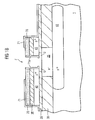
- Fig. 2 is a schematic representation of a known DPSA transistor, as shown TF Meister et al., IEDM Technical Digest 1995, p.739-741 known.
- numeral 1 denotes a silicon semiconductor substrate, 10 a n + subcollector region in the form of a buried layer, 20 p + channel blocking regions, 25 an n - collector region, 30 a p base region, 35 and 35a a 15 a LOCOS isolation oxide layer, 40 a p + base terminal, 45 an n + collector contact, 55 a silicon oxide / silicon nitride double spacer, and 60 an n + emitter contact.
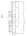
- Fig. 3a-c are schematic representations of the process steps with respect to the emitter contact with oxide spacer insulation of a conventional method for producing a DPSA transistor, in contrast to Fig. 2
- Reference symbol F denotes the emitter window in the layers 35 and 40.
- n + emitter contact After the formation of the oxide spacer 55 ', which covers the sidewalls of the emitter window F, an n + -doped (implanted or in-situ doped) n + on the active p + base region is formed in the DPSA transistor.
- Polysilicon layer 60 polycrystalline applied to the active transistor region and on the surrounding isolation regions.
- the n + polysilicon layer 60 is anisotropically patterned by means of a photographic technique to form the final emitter contact 60, and the n + dopant, for example, 20 nm, is driven into the underlying monocrystalline Si material of the base region 30 with a temperature step ( Fig. 3c ).
- the n + emitter is formed, which consists of a monocrystalline portion 31 and a polycrystalline portion 60, between which there is a very thin natural oxide layer 36 which forms after the spacer etch.
- the object of the invention is to specify an improved method for producing a bipolar semiconductor component, in particular a bipolar transistor, and a corresponding bipolar semiconductor component, which shows even further improved high-frequency characteristics.
- This object is achieved by a method for producing a bipolar semiconductor component, in particular a bipolar transistor, according to claim 1 and a corresponding bipolar semiconductor component according to claim 6.
- the idea on which the present invention is based is to generate a self-aligned gas or vacuum insulation by first producing a spacer between the base and emitter connection regions, which is selectively removed again after the emitter has been completed, relative to the emitter and base connection regions that a gap arises between these connection areas. Subsequently, the gap between the emitter and base connection region is closed by an incompletely compliant deposition of a dielectric and filled or evacuated with a predetermined gas atmosphere, but not filled again with a solid-state dielectric.
- Components according to the invention can be produced in comparison to components manufactured today without a significant change in the process control. All that is needed is a modified or additional wet-chemical etching and a non-conforming deposition. This results in the improved electrical properties even without significant additional costs.
- the first semiconductor region is a base region of a bipolar transistor, below which an associated collector region of the second conductivity type is formed beforehand, the second semiconductor region being the associated emitter region.
- the first insulation region and the sidewall spacer 80 are made of the same semiconductor material, in particular silicon oxide, and are selectively removed in the same etching process with respect to the first and second semiconductor regions.
- the second isolation region is formed by non-conformal deposition and planarization of an insulation material.
- the semiconductor component is a DPSA transistor.
- the transit frequency is dominated by the term proportional to 1 / I C. This, in turn, is dominated by the base-emitter capacitance, because typically C BE is a few factors greater than C BC . For fast transistors, ie large transit frequency therefore C BE must be minimized.
- the ratio of active base-emitter capacitance C BEa to spacer capacity C sp typically about 8: 1. Assuming, for example, a reduction of the emitter width and the spacer layer thickness by a factor of 2, the ratio is already 4: 2. The spacer capacity thus becomes a performance-limiting factor as component scaling progresses.
- the field strength in the emitter-base space charge zone must not be too large. This limits the maximum usable in practice dopant concentration at the emitter-base junction to values of less than about 5x10 18 cm -3 . Higher dopant concentrations would be desirable, for example, to reduce the base resistance of the transistor.
- the underlying principle of the invention is a dielectric in the form of a gas or vacuum insulation instead the known Fest stresses to use, which has a much lower dielectric constant.
- Such an emitter-base insulation has a smaller spacer capacitance by a factor of 3.9 or 7.5 in comparison with the oxide or nitride insulation used today.
- the mentioned emitter-base degradation should be significantly reduced because there is no spacer dielectric in which charge carrier traps can be generated by hot carrier stress.
- Fig. 1a-g are schematic representations of the method steps of an inventive embodiment of the method for producing a DPSA transistor.
- Fig. 1a shows the state of the DPSA transistor before integration of the SiGe base.
- the known shallow trench isolation is used here.
- the n - doped collector 25 is laterally isolated by the CVD oxide regions 35.
- the n - -doped collector 25 lies on the low-resistance, high-as-doped subcollector 10.
- the n - collector 25 is covered by a 40-80 nm-thick CVD oxide layer 35 '.
- On the CVD oxide layer 35 ' is a stack consisting of the p + polysilicon base terminal 40, a further CVD oxide layer 35 "and a nitride layer 70.
- the sidewalls of the emitter window F located above the n - -doped collector 25 are of The nitride layer 71 used for the production of this spacer 71a serves at the same time as the outside of the emitter window F Protect located isolation regions of the CVD oxide layer 35 'before the subsequent wet etching.
- the CVD oxide layer 35 'in the emitter window F is selectively removed to the surrounding nitride spacer 71a.
- This isotropic etching is carried out until self-aligned, a p + -polysilicon overhang U of about 80 nm is formed.
- the p + -doped SiGe base 32 and the low-doped Si cap (n- or p-) 34 are deposited in a CVD reactor on the exposed silicon region of the n - collector 25 by selective epitaxy, as in FIG Fig. 2c shown.
- C (1 ⁇ 10 18 cm -3 - 1 ⁇ 10 20 cm -3 ) is also prepared in the p + -doped SiGe base Fig. 1c installed in order to avoid the diffusion of the boron atoms during the subsequent process steps as far as possible.
- the selective deposition of the SiGe / Si layers 32, 34 is carried out until a low-resistance contact with the exposed p + polysilicon of the base terminal is achieved. Thereafter, the nitride spacers 71a and the other nitride auxiliary layers 70, 71 in phosphoric acid are selectively removed to oxide and Si.
- oxide spacers 80 are attached to the sidewalls of the emitter window F, which later isolate the p + base terminal 40 from the n + -doped emitter regions, and the other side edges of the p + base terminal 40 in the deposition of the n + -.
- Protect doped emitter polysilicon is attached to the sidewalls of the emitter window F, which later isolate the p + base terminal 40 from the n + -doped emitter regions, and the other side edges of the p + base terminal 40 in the deposition of the n + -.
- n + -doped polycrystalline emitter layer 60 over the entire surface by means.
- a thin nitride layer 90 of about 20 nm is applied to the n + -doped emitter layer 60, and the resulting double layer is applied by means of a photographic technique anisotropically structured.
- the n + dopant for example, 20 nm into the underlying monocrystalline Si material of the base cap portion 34 is driven to the in Fig. 2g not shown monocrystalline emitter region (see. Fig. 3c ) to build.
- a resist mask M is attached to the p + -type polysilicon terminal region of the DPSA transistor, which prevents undesired etching of specific chip areas (eg, the isolation regions or other components) during a subsequent etching process.
- the CVD oxide layer 35 "and the spacers 80 are selectively removed by etching to silicon, for example, hydrofluoric acid.”
- the spacer 80 is made of the same material as the CVD oxide layer 35 "over the base terminal region 40
- the etching time of the etching can be extended accordingly. If it is made of a different material, it is necessary to change the etching medium for etching the spacer after etching the CVD oxide layer 35 ", the transistor is now in the state as it is in FIG Figure 1f is shown. Between the emitter region 60 and the base connection region 40, the desired air gap LS has now emerged.
- Fig. 1g removes the mask M and generates a silicide layer 95 on the exposed areas of the p + polysilicon of the base terminal 40.
- a SiO 2 layer is deposited and planarized by chemical-mechanical polishing, so that an approximately 1500 nm thick intermediate oxide layer 100 is formed, which covers the entire transistor and closes the spacer air gap LS, without filling itself up again.
- This requires a deposition process that is not completely edge-covering (conforming).
- the deposition processes for the dielectrics between the transistor and the first metallization level have these properties anyway that no conversion of the process control is necessary. Air gaps LS with some 10 nm diameter can easily be closed without filling them up.
- Fig. 1g shows the completed DPSA transistor, in which still W-contacts 96, 97, 98 are provided, with which lines 110, for example made of AlCu, are connected.
- the inventive method has been described using a self-aligned double polysilicon transistor with réellespacer. However, it is in principle suitable for all components with thin spacers.
Abstract
Description
Die vorliegende Erfindung betrifft ein Verfahren zur Herstellung eines bipolaren Halbleiterbauelements, insbesondere eines Bipolartransistors, und ein entsprechendes bipolares Halbleiterbauelement.The present invention relates to a method for producing a bipolar semiconductor component, in particular a bipolar transistor, and to a corresponding bipolar semiconductor component.
Um die Anschlussbereiche von Emitter und Basis in Bipolartransistoren voneinander elektrisch zu isolieren, stehen prinzipiell zwei Methoden zur Verfügung: Zum einen können die Anschlussbereiche mit Hilfe von Fotolithografie für die Emitter- und Basisbereiche definiert und mit Hilfe von Ätztechnik strukturiert werden. Man nennt solche Transistoren daher justierte Transistoren. Der Abstand zwischen Emitter und Basisanschluss ist dann durch die minimal verfügbare Lithografiebreite gegeben. Da mit lithografischen Verfahren nur Auflösungen von bis zu 0.1 µm erreicht werden können, ist dieses Verfahren nicht für skalierte Bipolartransistoren geeignet, bei denen der Emitter nur einige 0.1 µm breit ist und der Isolationsbereich zwischen Emitter und Basis noch deutlich kleiner sein sollte (typisch einige 10 nm). Zudem tritt bei einer Justierung von Emitter- zu Basisebene immer eine Unsymmetrie im Stromfluss auf, da aufgrund der Justiertoleranz von Emitter- zu Basisebene eine Seite des Emitters immer näher zum Basisanschlussgebiet liegt als die gegenüberliegende. Justierte Transistoren sind daher für moderne skalierte Höchstperformance- Transistoren ungeeignet.In principle, in order to electrically isolate the connection regions of emitter and base in bipolar transistors, two methods are available: On the one hand, the connection regions can be defined by means of photolithography for the emitter and base regions and patterned with the aid of etching technology. These transistors are therefore called tuned transistors. The distance between emitter and base terminal is then given by the minimum available lithography width. Since only resolutions of up to 0.1 μm can be achieved with lithographic methods, this method is not suitable for scaled bipolar transistors, in which the emitter is only a few 0.1 μm wide and the isolation region between emitter and base should still be significantly smaller (typically some 10 μm) nm). In addition, an adjustment of the emitter to the base level always results in an asymmetry in the current flow, since, due to the adjustment tolerance from the emitter to the base level, one side of the emitter is always closer to the base connection region than the opposite one. Adjusted transistors are therefore unsuitable for modern scaled high-performance transistors.
Fast alle derzeitigen Transistoren werden daher als durch ein Emitterfenster selbstjustierte Transistoren ausgeführt. Die Emitter- und Basisanschlussbereiche werden dabei durch Polysiliziumschichten gebildet, die durch ein Dielektrikum (Siliziumoxid oder Siliziumnitrid) voneinander getrennt sind, weshalb sie auch als DPSA(selbstjustierte Doppel-Polysilizium)-Transistoren bezeichnet werden.Almost all current transistors are therefore implemented as transistors self-aligned by an emitter window. The emitter and base terminal regions are thereby formed by polysilicon layers which are separated from one another by a dielectric (silicon oxide or silicon nitride), for which reason they are also referred to as DPSA (self-aligned double polysilicon) transistors.
Das Dielektrikum wird als "Spacer" ausgebildet, d. h. durch anisotropes Rückätzen einer ganzflächig abgeschiedenen Schicht erzeugt, so dass im Emitterfenster die Spacer als Ätzresiduen übrig bleiben. Die Spacerbreite wird dabei durch die Dicke der Spacerschicht bestimmt und kann daher deutlich kleiner sein als Strukturen, die durch lithografische Verfahren erzeugt werden (im Prinzip nur wenige nm, typisch sind heute einige 10 nm). Daher ist dieses Verfahren zur Herstellung extrem skalierter DPSA-Transistoren geeignet.The dielectric is formed as a "spacer", d. H. produced by anisotropic etching back a layer deposited over the entire surface, so that in the emitter window, the spacers remain as Ätzresiduen. The spacer width is determined by the thickness of the spacer layer and can therefore be significantly smaller than structures that are produced by lithographic methods (in principle, only a few nm, typical today are some 10 nm). Therefore, this method is suitable for producing extremely scaled DPSA transistors.
Der DPSA-Transistor kann sowohl eine implantierte Si-Basis als auch eine epitaktisch abgeschiedene SiGe-Basis enthalten. Der Kollektor ist üblicherweise über eine im Substrat vergrabene Buried Layer (auch als Subkollektor bezeichnet) angeschlossen. Aufgrund ihrer lateralen und vertikalen Skalierbarkeit und den geringen parasitären Kapazitäts- und Widerstandsanteilen ist die DPSA-Transistorstruktur für Höchstgeschwindigkeitsanwendungen am besten geeignet.The DPSA transistor may include both an implanted Si base and an epitaxially deposited SiGe base. The collector is usually connected via a buried layer buried in the substrate (also referred to as a subcollector). Due to their lateral and vertical scalability and low parasitic capacitance and resistance levels, the DPSA transistor structure is best suited for high-speed applications.
DPSA-Transistoren und entsprechende Herstellungsverfahren sind z.B. aus
In
Zur Herstellung des n+-Emitterkontakts wird beim DPSA-Transistor nach der Bildung des Oxidspacers 55', der die Seitenwände des Emitterfensters F bedeckt auf dem aktiven p+-Basisbereich eine n+-dotierte (implantiert oder in-situ dotiert) n+-Polysiliziumschicht 60 auf dem aktiven Transistorgebiet sowie auf den umliegenden Isolationsbereichen polykristallin aufgebracht.For the formation of the n + emitter contact, after the formation of the oxide spacer 55 ', which covers the sidewalls of the emitter window F, an n + -doped (implanted or in-situ doped) n + on the active p + base region is formed in the DPSA transistor.
Danach wird die n+-Polysiliziumschicht 60 zur Bildung des endgültigen Emitterkontakts 60 mittels einer Fototechnik anisotrop strukturiert und mit einem Temperaturschritt der n+-Dotierstoff z.B. 20 nm in das darunter liegende einkristalline Si-Material des Basisbereichs 30 eingetrieben (
Aufgabe der Erfindung ist es, ein verbessertes Verfahren zur Herstellung eines bipolaren Halbleiterbauelements, insbesondere eines Bipolartransistors, und ein entsprechendes bipolares Halbleiterbauelement anzugeben, welches noch weiter verbesserte Hochfrequenzeigenschaften zeigt.The object of the invention is to specify an improved method for producing a bipolar semiconductor component, in particular a bipolar transistor, and a corresponding bipolar semiconductor component, which shows even further improved high-frequency characteristics.
Diese Aufgabe wird durch ein Verfahren zur Herstellung eines bipolaren Halbleiterbauelements, insbesondere eines Bipolartransistors, nach Anspruch 1 und ein entsprechendes bipolares Halbleiterbauelement nach Anspruch 6 gelöst.This object is achieved by a method for producing a bipolar semiconductor component, in particular a bipolar transistor, according to
Die der vorliegenden Erfindung zugrundliegende Idee besteht darin, eine selbstjustierte Gas- bzw. Vakuumisolation dadurch zu erzeugen, dass zunächst ein Spacer zwischen den Basis- und Emitteranschlussbereichen erzeugt wird, der nach Fertigstellung des Emitters selektiv zu den Emitter- und Basisanschlussbereichen wieder entfernt wird, so dass ein Spalt zwischen diesen Anschlussbereichen entsteht. Anschließend wird durch eine nicht vollständig konforme Abscheidung eines Dielektrikums der Spalt zwischen Emitter- und Basisanschlussbereich verschlossen und mit einer vorbestimmten Gasatmosphäre gefüllt bzw. evakuiert, aber nicht wieder mit einem Festkörperdielektrikum gefüllt.The idea on which the present invention is based is to generate a self-aligned gas or vacuum insulation by first producing a spacer between the base and emitter connection regions, which is selectively removed again after the emitter has been completed, relative to the emitter and base connection regions that a gap arises between these connection areas. Subsequently, the gap between the emitter and base connection region is closed by an incompletely compliant deposition of a dielectric and filled or evacuated with a predetermined gas atmosphere, but not filled again with a solid-state dielectric.
Nicht nur die Hochfrequenzeigenschaften, sondern auch die Emitter-Basis-Degradation sollte durch solch einen Gas- bzw. Vakuumspacer deutlich verbessert sein, da kein Festköroerdielektrikum mehr vorhanden ist, in dem Traps erzeugt werden können. Damit sollten sich Transistoren realisieren lassen, die bei gleicher Dotierstoffverteilung bessere Langzeitstabilität aufweisen als Transistoren mit Dielektrikum. Die geringere Anfälligkeit gegen hot carrier stress könnte auch dazu genutzt werden, größere Dotierstoffkonzentrationen im Emitter-Basis-Bereich zu verwenden und damit den Basiswiderstand zu verringern. Dies ergäbe z. B. Transistoren mit höherer maximaler Oszillationsfrequenz, geringeren Gaterverzögerungszeiten und niedrigerem Rauschen.Not only the high frequency properties but also the emitter-base degradation should be significantly improved by such a gas or vacuum spacer, since there is no more solid-state dielectric in which traps can be generated. This should make it possible to realize transistors which, with the same dopant distribution, have better long-term stability than transistors with a dielectric. The lower susceptibility to hot carrier stress could also be exploited to use larger dopant concentrations in the emitter-base region and thus lower the base resistance. This would give z. B. transistors with higher maximum oscillation frequency, lower gate delay times and lower noise.
Erfindungsgemässe Bauelemente im Vergleich zu heute gefertigten Bauelementen ohne wesentliche Änderung der Prozessführung herstellbar sind. Man benötigt lediglich eine modifiezierte bzw. zusätzliche nasschemische Ätzung und eine nicht-konforme Abscheidung. Damit ergeben sich die verbesserten elektrischen Eigenschaften auch ohne nennenswerte Zusatzkosten.Components according to the invention can be produced in comparison to components manufactured today without a significant change in the process control. All that is needed is a modified or additional wet-chemical etching and a non-conforming deposition. This results in the improved electrical properties even without significant additional costs.
Bevorzugte Weiterbildungen sind Gegenstand der jeweiligen Unteransprüche.Preferred developments are the subject of the respective subclaims.
Gemäss einer bevorzugten Weiterbildung ist der erste Halbleiterbereich ein Basisbereich eines Bipolartransistors, unter dem zuvor ein zugehöriger Kollektorbereich des zweiten Leitungstyps gebildet wird, wobei der zweite Halbleiterbereich der zugehörige Emitterbereich ist.According to a preferred development, the first semiconductor region is a base region of a bipolar transistor, below which an associated collector region of the second conductivity type is formed beforehand, the second semiconductor region being the associated emitter region.
Gemäss einer weiteren bevorzugten Weiterbildung sind der erste Isolationsbereich und der Seitenwandspacer (80) aus demselben Halbleitermaterial, insbesondere Siliziumoxid, und werden im selben Ätzprozess selektiv gegenüber dem ersten und zweiten Halbleiterbereich entfernt.According to a further preferred development, the first insulation region and the
Gemäss einer weiteren bevorzugten Weiterbildung wird der zweite Isolationsbereich durch nicht-konformes Abscheiden und Planarisieren eines Isolationsmaterials gebildet.According to a further preferred development, the second isolation region is formed by non-conformal deposition and planarization of an insulation material.
Gemäss einer weiteren bevorzugten Weiterbildung ist das Halbleiterbauelement ein DPSA-Transistor.According to a further preferred development, the semiconductor component is a DPSA transistor.
Nachfolgend wird die Erfindung anhand von Ausführungsbeispielen unter Bezugnahme auf die Zeichnungen näher erläutert.The invention will be explained in more detail by means of embodiments with reference to the drawings.
Es zeigen:
- Fig. 1a-g
- schematische Darstellungen der Verfahrensschritte einer erfindungsgemässen Ausführungsform des Ver- fahren zur Herstellung eines DPSA-Transistors;
- Fig. 2
- eine schematische Darstellung eines bekannten DPSA-Transiators; und
- Fig. 3a-c
- schematische Darstellungen der Verfahrensschritte hinsichtlich des Emitterkontakts mit Oxidspaceri- solation eines üblichen Verfahren zur Herstellung eines DPSA-Transistors.
- Fig. 1a-g
- schematic representations of the method steps of an inventive embodiment of the method for producing a DPSA transistor;
- Fig. 2
- a schematic representation of a known DPSA transiator; and
- Fig. 3a-c
- schematic representations of the process steps with respect to the emitter contact with Oxidspaceri- solation of a conventional method for producing a DPSA transistor.
In den Figuren gleiche Bezugszeichen bezeichnen gleiche oder gleich wirkende Elemente.In the figures, the same reference numerals designate the same or equivalent elements.
Die der vorliegenden Erfindung zugrundeliegenden Gedanken setzen bei 
wobei
- fT
- Transitfrequenz
- τf
- Transitzeit
- RC
- Kollektorwiderstand
- RE
- Emitterwiderstand
- CBC
- Basis-Kollektor-Kapazität
- CBE
- Basis-Emitterkapazität
- IC
- Kollektorstrom
- UT
- Thermospannung
in which
- f T
- transit frequency
- τ f
- transit time
- R C
- collector resistance
- R E
- emitter resistor
- C BC
- Base-collector capacitance
- C BE
- Base-emitter capacitance
- I C
- collector current
- U T
- thermovoltage
Man sieht, dass für kleine Kollektorströme die Transitfrequenz durch den Term proportional 1/IC dominiert wird. Dieser wiederum wird durch die Basis-Emitter-Kapazität dominiert, weil typischerweise CBE um einige Faktoren größer als CBC ist. Für schnelle Transistoren, d.h. große Transitfrequenz muss daher CBE minimiert werden.It can be seen that for small collector currents, the transit frequency is dominated by the term proportional to 1 / I C. This, in turn, is dominated by the base-emitter capacitance, because typically C BE is a few factors greater than C BC . For fast transistors, ie large transit frequency therefore C BE must be minimized.
Die aktive Basis-Emitter-Kapazität im Emitter-Basis-Bereich wird durch die Skalierung der Bauteile stetig verkleinert, indem die Emitterfläche reduziert wird. Dafür ist gleichzeitig auch die Verringerung der Spacerschichtdicke nötig, damit der Spacer im immer kleineren Emitterfenster erzeugt werden kann ohne dieses vollständig zu füllen. Damit steigt aber die Spacerkapazität, die invers proportional zur Schichtdicke ist: 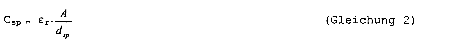
wobei
- Csp
- Spacerkapazität
- εr
- Dieelektrizitätskonstante des Spacermaterials
- A
- Fläche der Spacerkapazität (Emitter- zu Basispolysilizi- um,)
- dsp
- Dicke der Spacerschicht
in which
- C sp
- spacer capacitance
- ε r
- The dielectric constant of the spacer material
- A
- Area of spacer capacitance (emitter to base polysilicon,)
- d sp
- Thickness of the spacer layer
Bei heutigen Transistoren (aktive Emitterbreite z.B. typisch 200 nm und Spacerschichtdicke z.B. typisch 40 nm) beträgt das Verhältnis von aktiver Basis-Emitter-Kpazität CBEa zu Spacerkapazität Csp typisch ca. 8:1. Nimmt man z.B. eine Reduzierung der Emitterbreite und der Spacerschichtdicke jeweils um einen Faktor 2 an, beträgt das Verhältnis bereits 4:2. Die Spacerkapazität wird damit mit fortschreitender Bauteilskalierung zum Performance limitierenden Faktor.In today's transistors (active emitter width, for example typically 200 nm and spacer layer thickness, for example, typically 40 nm), the ratio of active base-emitter capacitance C BEa to spacer capacity C sp typically about 8: 1. Assuming, for example, a reduction of the emitter width and the spacer layer thickness by a factor of 2, the ratio is already 4: 2. The spacer capacity thus becomes a performance-limiting factor as component scaling progresses.
Aus Gleichung 2 ist ersichtlich, dass die Spacerkapazität deutlich verringert werden könnte, wenn statt des Dielektrikums Siliziumoxid (εr=3.9) oder Siliziumnitrid (εr=7.5) ein Isolationsmaterial mit kleinerer Dielektrizitätskonstante verwendet werden könnte.From equation 2 it can be seen that the spacer capacitance could be significantly reduced if, instead of the dielectric silicon oxide (ε r = 3.9) or silicon nitride (ε r = 7.5), an insulating material with a smaller dielectric constant could be used.
Ein weiterer Nachteil einer Emitter-Basis-Isolation aus Dielektrikum ist die Anfälligkeit gegenüber hot carrier stress (siehe z.B.
Um die Emitter-Basis-Degradation möglichst zu vermeiden, darf die Feldstärke in der Emitter-Basis-Raumladungszone nicht zu groß werden. Dies begrenzt die in der Praxis maximal verwendbare Dotierstoffkonzentration am Emitter-Basis-Übergang auf Werte von kleiner etwa 5x1018 cm-3 . Höhere Dotierstoffkonzentrationen wären aber wünschenswert um z.B. den Basiswiderstand des Transistors zu verringern.In order to avoid the emitter-base degradation as much as possible, the field strength in the emitter-base space charge zone must not be too large. This limits the maximum usable in practice dopant concentration at the emitter-base junction to values of less than about 5x10 18 cm -3 . Higher dopant concentrations would be desirable, for example, to reduce the base resistance of the transistor.
Das der Erfindung zugrundeliegende Prinzip besteht darin, ein Dielektrikum in Form einer Gas- bzw. Vakuumisolation anstelle des bekannten Festkörperspacers zu verwenden, die eine wesentlich geringere Dielektrizitätskonstante aufweist. Der kleinstmögliche Wert wäre εr=1, d.h. eine Isolation mit Vakuum oder bestimmten Gasen (z.B. Luft). Eine solche Emitter-Basis-Isolation hat im Vergleich zu heute verwendeten Isolationen aus Oxid bzw. Nitrid eine um einen Faktor 3.9 bzw. 7.5 kleinere Spacerkapazität. Außerdem sollte die erwähnte Emitter-Basis-Degradation deutlich reduziert sein, weil kein Spacerdielektrikum vorhanden ist, in dem durch hot carrier stress Ladungsträgertraps erzeugt werden können.The underlying principle of the invention is a dielectric in the form of a gas or vacuum insulation instead the known Festkörperpacers to use, which has a much lower dielectric constant. The smallest possible value would be ε r = 1, ie insulation with vacuum or certain gases (eg air). Such an emitter-base insulation has a smaller spacer capacitance by a factor of 3.9 or 7.5 in comparison with the oxide or nitride insulation used today. In addition, the mentioned emitter-base degradation should be significantly reduced because there is no spacer dielectric in which charge carrier traps can be generated by hot carrier stress.
Ein bekanntes Herstellungsverfahren für den mittels selektiver SiGe-Basis-Epitaxie hergestellten DPSA-Transistor ist, wie oben erwähnt, z.B. in der
Mittels dieser Nassätzung wird, wie in Fig. lb gezeigt, die CVD-Oxidschicht 35' im Emitterfenster F selektiv zu dem umgebenden Nitridspacer 71a entfernt. Diese isotrope Ätzung wird solange durchgeführt, bis selbstjustiert ein p+-Polysilizium-Überhang U von ca. 80 nm entstanden ist.By means of this wet etching, as shown in FIG. 1b, the
Die p+-dotierte SiGe-Basis 32 und die niedrig dotierte Si-Kappe (n- oder p-) 34 werden in einem CVD-Reaktor mittels selektiver Epitaxie auf dem freiliegenden Siliziumbereich des n--Kollektors 25 abgeschieden, wie in
Bei der selektiven Epitaxie wird in der p+-dotierten SiGe-Basis auch C (1·1018 cm-3 - 1·1020 cm-3) gemäss
Danach werden gemäss Fig. ld Oxidspacer 80 an den Seitenwänden des Emitterfensters F angebracht, die später den p+-Basisanschluss 40 von den n+-dotierten Emitterbereichen isolieren bzw. die anderen Seitenkanten des p+-Basisanschlusses 40 bei der Abscheidung des n+-dotierten Emitterpolysiliziums schützen.Thereafter, as shown in FIG. 1d,
Dann wird gemäss
Danach wird gemäss
Nun werden die CVD-Oxidschicht 35 " und die Spacer 80 durch eine Ätzung selektiv zu Silizium entfernt, z. B. mit Flusssäure. Ist der Spacer 80 wie beim vorliegenden Beispiel aus dem gleichen Material wie die CVD-Oxidschicht 35 " über dem Basisanschlussbereich 40, so kann im Vergleich zum bekannten Prozess einfach die Ätzzeit der Ätzung entsprechend verlängert werden. Ist er aus einem anderen Material, muss nach Ätzung der CVD-Oxidschicht 35 " das Ätzmedium zur Ätzung des Spacers gewechselt werden. Der Transistor befindet sich nun in dem Zustand wie er in
Anschliessend wird gemäss
Das erfindungsgemässe Verfahren wurde anhand eines selbstjustierten Doppel-Polysilizium-Transistors mit Innenspacer beschrieben. Es ist prinzipiell jedoch für alle Bauteile mit dünnen Spacern geeignet.The inventive method has been described using a self-aligned double polysilicon transistor with Innenspacer. However, it is in principle suitable for all components with thin spacers.
- 2525
- Kollektorbereichcollector region
- 3030
- Basisbereichbase region
- 35,35a,35',35"35,35a, 35 ', 35 "
- Oxidschichtoxide
- 4040
- BasisanschlussbereichBase terminal region
- 8080
- Oxid-SeitenwandspacerOxide sidewall
- 6060
- polykristalline Emitterschichtpolycrystalline emitter layer
- FF
- Emitterfensteremitter window
- 11
- Siliziumsubstratsilicon substrate
- 1010
- Subkollektorbereichsubcollector region
- 70,7170.71
- Nitridschichtnitride
- 71a71a
- Nitrid-SeitenwandspacerNitride sidewall spacers
- UU
- Überhangoverhang
- 3232
- BasisgrundschichtBased basecoat
- 3434
- BasiskappenschichtBase cap layer
- 9090
- Nitridmaskenitride
- MM
- Fotomaskephotomask
- 100100
- Zwischendielektrikumintermediate dielectric
- 96,97,9896,97,98
- Kontaktecontacts
- 110110
- Verdrahtungwiring
- 9595
- Silizidsilicide
Claims (9)
- A method for manufacturing a bipolar semiconductor device, particularly a bipolar transistor, comprising the steps of:Providing a first semiconductor region (32, 34) of a first conductivity type (p) on a semiconductor substrate (1);providing a connecting region (40) of said first conductivity type (p+) on the first semiconductor region (32, 34);providing a first insulating region (35") on the connecting region (40);forming a window (F) in the first insulating region (35") and connecting region (40) for at least partially exposing the first semiconductor region (32, 34);providing a first sidewall spacer (80) in the window (F) for insulating the connecting region (40);providing a second semiconductor region (60) of the second conductivity type (n+) in the window such that it covers the sidewall spacer (80) and a part of the surrounding first insulating region (35");
characterized byremoving the surrounding first insulating region (35") and the sidewall spacer (80) for forming a gap (LS) between the connecting region (40) and the second semiconductor region (60); andclosing the gap (LS) with a second insulating region (100) while simultaneously providing a gas or vacuum atmosphere in the closed gap (LS). - The method of claim 1,
wherein the first semiconductor region (32, 34) is a base region of a bipolar transistor under which a corresponding collector region (25) of the second conductivity type (n-) is formed before, and wherein the second conductivity region (60) is the corresponding emitter region. - The method of claim 1 or 2,
wherein the first insulating region (35") and the sidewall spacer (80) are made of the same material, particularly silicon oxide, and are selectively removed in the same etching process with respect to the first and second semiconductor region (40; 60). - The method of claim 1, 2 or 3,
wherein the second insulating region (100) is formed by non-conformal deposition and planarization of an insulating material. - The method according to one of the preceding claims,
wherein the semiconductor device is a DPSA transistor. - A bipolar semiconductor device, particularly a bipolar transistor, comprising:a first semiconductor region (32, 34) of a first conductivity type (p) on a semiconductor substrate (1);a connecting region (40) of the first conductivity type (p+) in connection with the semiconductor region (32, 34);a window (F) in the connecting region (40) which at least partially exposes the first semiconductor region (32, 34);a second semiconductor region (60) of the second conductivity type (n+) in the window (F) and partially covering the surrounding connecting region (40);
characterized bya gap (LS) between the connecting region (40) and the second semiconductor region (60); andan insulating region (100) for closing the gap (LS) under a gas or vacuum atmosphere. - The semiconductor device according to claim 6,
wherein the first semiconductor region (32, 34) is a base region of a bipolar transistor under which a corresponding collector region (25) of the second conductivity type (n-) is formed before, and wherein the second semiconductor region (60) is the corresponding emitter region. - The semiconductor device according to claims 6 or 7,
wherein the second insulating region (100) is formed by a non-confomally deposited and planarized insulating material. - The semiconductor device according to one of claims 6 to 8,
wherein the semiconductor device is a DPSA transistor.
Applications Claiming Priority (2)
| Application Number | Priority Date | Filing Date | Title |
|---|---|---|---|
| DE10316529 | 2003-04-10 | ||
| PCT/EP2004/003805 WO2004090988A1 (en) | 2003-04-10 | 2004-04-08 | Method for the production of a bipolar semiconductor element, especially a bipolar transistor, and corresponding bipolar semiconductor component |
Publications (2)
| Publication Number | Publication Date |
|---|---|
| EP1611615A1 EP1611615A1 (en) | 2006-01-04 |
| EP1611615B1 true EP1611615B1 (en) | 2011-08-31 |
Family
ID=33154152
Family Applications (1)
| Application Number | Title | Priority Date | Filing Date |
|---|---|---|---|
| EP04726497A Expired - Fee Related EP1611615B1 (en) | 2003-04-10 | 2004-04-08 | Method for the production of a bipolar semiconductor element, especially a bipolar transistor, and corresponding bipolar semiconductor component |
Country Status (5)
| Country | Link |
|---|---|
| US (1) | US7285470B2 (en) |
| EP (1) | EP1611615B1 (en) |
| JP (1) | JP4202389B2 (en) |
| CN (1) | CN100472801C (en) |
| WO (1) | WO2004090988A1 (en) |
Families Citing this family (9)
| Publication number | Priority date | Publication date | Assignee | Title |
|---|---|---|---|---|
| DE102006011240A1 (en) * | 2006-03-10 | 2007-09-20 | Infineon Technologies Ag | Bipolar transistor and method of manufacturing a bipolar transistor |
| US7687887B1 (en) * | 2006-12-01 | 2010-03-30 | National Semiconductor Corporation | Method of forming a self-aligned bipolar transistor structure using a selectively grown emitter |
| US7679164B2 (en) | 2007-01-05 | 2010-03-16 | International Business Machines Corporation | Bipolar transistor with silicided sub-collector |
| DE102009001552A1 (en) * | 2008-12-12 | 2010-06-17 | Ihp Gmbh - Innovations For High Performance Microelectronics / Leibniz-Institut Für Innovative Mikroelektronik | Bipolar transistor with self-aligned emitter contact |
| US9166067B2 (en) | 2012-06-12 | 2015-10-20 | Taiwan Semiconductor Manufacturing Co., Ltd. | Device layout for reference and sensor circuits |
| US8736355B2 (en) * | 2012-06-12 | 2014-05-27 | Taiwan Semiconductor Manufacturing Co., Ltd. | Device layout for reference and sensor circuits |
| US9231074B2 (en) | 2013-07-19 | 2016-01-05 | Globalfoundries Inc. | Bipolar junction transistors with an air gap in the shallow trench isolation |
| US10211090B2 (en) | 2016-10-12 | 2019-02-19 | Globalfoundries Inc. | Transistor with an airgap for reduced base-emitter capacitance and method of forming the transistor |
| US10453919B2 (en) | 2017-11-06 | 2019-10-22 | Stmicroelectronics (Crolles 2) Sas | Heterojunction bipolar transistor with counter-doped collector region and increase collector dependent breakdown voltage |
Family Cites Families (8)
| Publication number | Priority date | Publication date | Assignee | Title |
|---|---|---|---|---|
| JP2971246B2 (en) | 1992-04-15 | 1999-11-02 | 株式会社東芝 | Method for manufacturing hetero bipolar transistor |
| DE19748523C2 (en) * | 1997-11-03 | 1999-10-07 | Siemens Ag | Semiconductor component, method for producing such a semiconductor component and use of the method |
| US6693335B2 (en) * | 1998-09-01 | 2004-02-17 | Micron Technology, Inc. | Semiconductor raised source-drain structure |
| DE19958062C2 (en) | 1999-12-02 | 2002-06-06 | Infineon Technologies Ag | Method for producing a bipolar transistor and method for producing an integrated circuit arrangement with such a bipolar transistor |
| US6346453B1 (en) * | 2000-01-27 | 2002-02-12 | Sige Microsystems Inc. | Method of producing a SI-GE base heterojunction bipolar device |
| DE10014660C2 (en) * | 2000-03-24 | 2002-08-29 | Infineon Technologies Ag | Semiconductor arrangement with a trench electrode separated by a cavity from a drift path |
| FR2806831B1 (en) * | 2000-03-27 | 2003-09-19 | St Microelectronics Sa | METHOD FOR MANUFACTURING A BIPOLAR SELF-ALIGNED DOUBLE-POLYSILICIUM TYPE BIPOLAR TRANSISTOR AND CORRESPONDING TRANSISTOR |
| DE10125019A1 (en) | 2001-05-22 | 2002-12-05 | Infineon Technologies Ag | Void structure, multiple void structure and method of making a void structure |
-
2004
- 2004-04-08 JP JP2006500088A patent/JP4202389B2/en not_active Expired - Fee Related
- 2004-04-08 EP EP04726497A patent/EP1611615B1/en not_active Expired - Fee Related
- 2004-04-08 CN CNB2004800095114A patent/CN100472801C/en not_active Expired - Fee Related
- 2004-04-08 WO PCT/EP2004/003805 patent/WO2004090988A1/en active Application Filing
-
2005
- 2005-09-30 US US11/240,297 patent/US7285470B2/en not_active Expired - Fee Related
Also Published As
| Publication number | Publication date |
|---|---|
| US20060040456A1 (en) | 2006-02-23 |
| US7285470B2 (en) | 2007-10-23 |
| CN100472801C (en) | 2009-03-25 |
| CN1771605A (en) | 2006-05-10 |
| JP2006523010A (en) | 2006-10-05 |
| JP4202389B2 (en) | 2008-12-24 |
| EP1611615A1 (en) | 2006-01-04 |
| WO2004090988A1 (en) | 2004-10-21 |
Similar Documents
| Publication | Publication Date | Title |
|---|---|---|
| DE102010001290B4 (en) | Bipolar transistor with base-collector insulation without dielectric and method for producing such a | |
| EP2830097B1 (en) | Bipolar transistor having self-adjusted emitter contact and method of manufacturing the same | |
| EP0036634B1 (en) | Method of making a bipolar transistor structure | |
| DE10308870B4 (en) | Bipolar transistor with improved base-emitter junction and method of manufacture | |
| EP1825504B1 (en) | Vertical bipolar transistor | |
| DE10297535B4 (en) | A method of fabricating a high voltage high speed MOS transistor by ion implantation | |
| EP1625614B1 (en) | Method for the production of a bipolar transistor | |
| EP1611615B1 (en) | Method for the production of a bipolar semiconductor element, especially a bipolar transistor, and corresponding bipolar semiconductor component | |
| WO2005109495A1 (en) | Method for producing a semiconductor circuit arrangement | |
| EP1741133B1 (en) | Method for producing a planar spacer, an associated bipolar transistor and an associated bicmos circuit arrangement | |
| DE10124032B4 (en) | Method of manufacturing components on an SOI wafer | |
| WO2003049191A2 (en) | Bicmos structure, method for producing the same and bipolar transistor for a bicmos structure | |
| EP1415340A2 (en) | Method for the parallel production of an mos transistor and a bipolar transistor | |
| EP1436842B1 (en) | Bipolar transistor and method for producing the same | |
| DE3915634A1 (en) | Bipolar high-frequency transistor and method for producing the transistor using the polysilicon self-alignment technique | |
| DE102015208133B3 (en) | BiMOS device with a fully self-aligned emitter silicon and method of making the same | |
| DE102004053393B4 (en) | Method for producing a vertically integrated cascode structure and vertically integrated cascode structure | |
| DE10328008B4 (en) | Integrated circuit arrangement with pnp and npn bipolar transistors and manufacturing method | |
| WO2004114408A1 (en) | Integrated circuit arrangement with npn and pnp bipolar transistors and corresponding production method | |
| DE10249897B4 (en) | Self-aligning process for producing a transistor | |
| EP1474826B1 (en) | Polysilicon bipolar transistor and method for producing the same | |
| DE112021005664T5 (en) | JUNCTION TRANSISTOR WITH VERTICALLY INTEGRATED RESISTOR | |
| WO2000017932A1 (en) | Bipolar transistor and method for producing same |
Legal Events
| Date | Code | Title | Description |
|---|---|---|---|
| PUAI | Public reference made under article 153(3) epc to a published international application that has entered the european phase |
Free format text: ORIGINAL CODE: 0009012 |
|
| 17P | Request for examination filed |
Effective date: 20050930 |
|
| AK | Designated contracting states |
Kind code of ref document: A1 Designated state(s): AT BE BG CH CY CZ DE DK EE ES FI FR GB GR HU IE IT LI LU MC NL PL PT RO SE SI SK TR |
|
| AX | Request for extension of the european patent |
Extension state: AL HR LT LV MK |
|
| DAX | Request for extension of the european patent (deleted) | ||
| RBV | Designated contracting states (corrected) |
Designated state(s): DE FR GB |
|
| RAP1 | Party data changed (applicant data changed or rights of an application transferred) |
Owner name: INFINEON TECHNOLOGIES AG |
|
| GRAP | Despatch of communication of intention to grant a patent |
Free format text: ORIGINAL CODE: EPIDOSNIGR1 |
|
| GRAS | Grant fee paid |
Free format text: ORIGINAL CODE: EPIDOSNIGR3 |
|
| GRAA | (expected) grant |
Free format text: ORIGINAL CODE: 0009210 |
|
| AK | Designated contracting states |
Kind code of ref document: B1 Designated state(s): DE FR GB |
|
| REG | Reference to a national code |
Ref country code: GB Ref legal event code: FG4D Free format text: NOT ENGLISH |
|
| REG | Reference to a national code |
Ref country code: DE Ref legal event code: R096 Ref document number: 502004012842 Country of ref document: DE Effective date: 20111027 |
|
| PLBE | No opposition filed within time limit |
Free format text: ORIGINAL CODE: 0009261 |
|
| STAA | Information on the status of an ep patent application or granted ep patent |
Free format text: STATUS: NO OPPOSITION FILED WITHIN TIME LIMIT |
|
| 26N | No opposition filed |
Effective date: 20120601 |
|
| REG | Reference to a national code |
Ref country code: DE Ref legal event code: R097 Ref document number: 502004012842 Country of ref document: DE Effective date: 20120601 |
|
| REG | Reference to a national code |
Ref country code: FR Ref legal event code: PLFP Year of fee payment: 13 |
|
| REG | Reference to a national code |
Ref country code: FR Ref legal event code: PLFP Year of fee payment: 14 |
|
| REG | Reference to a national code |
Ref country code: FR Ref legal event code: PLFP Year of fee payment: 15 |
|
| PGFP | Annual fee paid to national office [announced via postgrant information from national office to epo] |
Ref country code: FR Payment date: 20190418 Year of fee payment: 16 |
|
| PGFP | Annual fee paid to national office [announced via postgrant information from national office to epo] |
Ref country code: GB Payment date: 20190418 Year of fee payment: 16 Ref country code: DE Payment date: 20190624 Year of fee payment: 16 |
|
| REG | Reference to a national code |
Ref country code: DE Ref legal event code: R119 Ref document number: 502004012842 Country of ref document: DE |
|
| PG25 | Lapsed in a contracting state [announced via postgrant information from national office to epo] |
Ref country code: FR Free format text: LAPSE BECAUSE OF NON-PAYMENT OF DUE FEES Effective date: 20200430 Ref country code: DE Free format text: LAPSE BECAUSE OF NON-PAYMENT OF DUE FEES Effective date: 20201103 |
|
| GBPC | Gb: european patent ceased through non-payment of renewal fee |
Effective date: 20200408 |
|
| PG25 | Lapsed in a contracting state [announced via postgrant information from national office to epo] |
Ref country code: GB Free format text: LAPSE BECAUSE OF NON-PAYMENT OF DUE FEES Effective date: 20200408 |