EP1610434A1 - Schaltungsanordnung zur Begrenzung von Überspannungen bei Speichermodulen - Google Patents
Schaltungsanordnung zur Begrenzung von Überspannungen bei Speichermodulen Download PDFInfo
- Publication number
- EP1610434A1 EP1610434A1 EP05105267A EP05105267A EP1610434A1 EP 1610434 A1 EP1610434 A1 EP 1610434A1 EP 05105267 A EP05105267 A EP 05105267A EP 05105267 A EP05105267 A EP 05105267A EP 1610434 A1 EP1610434 A1 EP 1610434A1
- Authority
- EP
- European Patent Office
- Prior art keywords
- voltage
- vle
- memory
- limiting
- elements
- Prior art date
- Legal status (The legal status is an assumption and is not a legal conclusion. Google has not performed a legal analysis and makes no representation as to the accuracy of the status listed.)
- Withdrawn
Links
Images


Classifications
-
- H—ELECTRICITY
- H02—GENERATION; CONVERSION OR DISTRIBUTION OF ELECTRIC POWER
- H02J—ELECTRIC POWER NETWORKS; CIRCUIT ARRANGEMENTS OR SYSTEMS FOR SUPPLYING OR DISTRIBUTING ELECTRIC POWER; SYSTEMS FOR STORING ELECTRIC ENERGY
- H02J7/00—Circuit arrangements for charging or discharging batteries or for supplying loads from batteries
- H02J7/50—Circuit arrangements for charging or discharging batteries or for supplying loads from batteries acting upon multiple batteries simultaneously or sequentially
- H02J7/52—Circuit arrangements for charging or discharging batteries or for supplying loads from batteries acting upon multiple batteries simultaneously or sequentially for charge balancing, e.g. equalisation of charge between batteries
- H02J7/54—Passive balancing, e.g. using resistors or parallel MOSFETs
-
- H—ELECTRICITY
- H02—GENERATION; CONVERSION OR DISTRIBUTION OF ELECTRIC POWER
- H02J—ELECTRIC POWER NETWORKS; CIRCUIT ARRANGEMENTS OR SYSTEMS FOR SUPPLYING OR DISTRIBUTING ELECTRIC POWER; SYSTEMS FOR STORING ELECTRIC ENERGY
- H02J7/00—Circuit arrangements for charging or discharging batteries or for supplying loads from batteries
- H02J7/60—Circuit arrangements for charging or discharging batteries or for supplying loads from batteries including safety or protection arrangements
- H02J7/64—Circuit arrangements for charging or discharging batteries or for supplying loads from batteries including safety or protection arrangements against overvoltage
-
- H—ELECTRICITY
- H02—GENERATION; CONVERSION OR DISTRIBUTION OF ELECTRIC POWER
- H02J—ELECTRIC POWER NETWORKS; CIRCUIT ARRANGEMENTS OR SYSTEMS FOR SUPPLYING OR DISTRIBUTING ELECTRIC POWER; SYSTEMS FOR STORING ELECTRIC ENERGY
- H02J7/00—Circuit arrangements for charging or discharging batteries or for supplying loads from batteries
- H02J7/34—Parallel operation in networks using both storage and other DC sources, e.g. providing buffering
- H02J7/345—Parallel operation in networks using both storage and other DC sources, e.g. providing buffering using capacitors as storage or buffering devices
Definitions
- the invention relates to a circuit arrangement for limiting overvoltages in memory modules composed of memory elements, comprising a series circuit of n memory elements, wherein the Series connection between a first potential and a second potential connected is and the n memory elements voltage-limiting elements assigned.
- Memory modules are used to store electrical energy.
- the storage capacity Of conventional memory elements is usually less than the required total amount of energy to be stored. Usually that is maximum allowable voltage across a memory element less than the voltage required for the application. That's why there are several storage elements with less storage capacity to a memory module combined.
- Typical storage elements are as capacitors or accumulators designed.
- a special type of capacitors form supercapacities (SCAP). These supercapacitors are also called thin-film capacitors, referred to as Ultracaps, Boostcaps or Supercaps. such Supercapacities are becoming increasingly important as electrical energy storage devices for a variety of applications, for example in the automotive industry or in portable electrical appliances, where very fast high amounts of charge must be stored or released.
- a single supercapacitor can only be operated with a permissible voltage U max of 2.3 V to 2.5 V, so that for most applications several supercapacities are interconnected in a series circuit and a memory module with a maximum voltage of N * U max is formed ,
- Supercapacitors are subject to a manufacturing tolerance that can translate into a capacity variation of -10% to +30%.
- aging can cause capacity losses of about 20%.
- the aging process of supercapacitors is temperature-dependent and thus not the same for all supercapacities contained in a memory module. This results in a charging of a supercapacitor-containing memory module, an uneven voltage distribution between the individual memory elements.
- the supercapacitor which has the smallest capacity due to the aging process, is subjected to the highest voltage in the series connection.
- WO 02/15363 A2 From WO 02/15363 A2 is a power storage system with batteries and Capacitors are known in which supercapacitors are used. As As shown above, supercapacitors can not withstand overvoltage and must thus be monitored. In WO 02/15363 A2 several different Connection variants to avoid overvoltages described. It describes a Z-diode over several supercapacitors but only the voltage across all parallel to the zener diode limited supercapacitors and not via a super capacity alone. Thus, the single supercapacitance is not overvoltages protected.
- the supercapacitor indicates with the smaller capacity after charging a larger voltage on.
- the zener diode voltage is twice the permissible one Capacity of the super capacity is limited, the super capacity with the overloaded smaller capacity.
- an overvoltage protection for modules specify from memory elements that can be implemented easily and inexpensively is and reliable protection against damage from Memory elements guaranteed at surges.
- the invention is based on the idea that Z-diodes are cost-effective and easily switchable way to provide voltage limiting. Since memory elements usually have a low allowable voltage and therefore must be used in a series connection to to store a larger amount of charge, it would be obvious Each memory element, as already known from the prior art is to connect a Z-diode with a low breakdown voltage in parallel, the maximum allowable voltage of the corresponding memory element equivalent. However, since the Z-diodes for low voltages a inclined, relatively soft characteristic already having a discharge current This is at voltages below the breakdown voltage disadvantageous for the overall efficiency of the memory module. The storage duration of the total module is due to the already flowing before the breakdown voltage Discharge current reduced. On the other hand, Z diodes have a higher Breakdown voltage a steeper characteristic, so only when it reaches the breakdown voltage a current flows.
- a circuit arrangement in which directly interconnects any combination of M's Memory elements, with M ⁇ 2, is selected from the series circuit and any possible combination of M directly related Memory elements connected in parallel a voltage-limiting element becomes.
- M denotes the maximum number of directly with each other connected memory elements of a given combination.
- Z diodes with a higher breakdown voltage than the maximum permissible voltage of a single memory element used become.
- an am first potential connected first memory element is monitored, is provided an am second potential connected n-th memory element also a voltage-limiting Switch element parallel. If M> 2 is chosen, also every subcombination of at least 2 is directly related to each other connected memory elements of the combination, the one at the first potential or has a storage element connected to the second potential, in each case a voltage-limiting element connected in parallel.
- the series circuit may comprise any number of memory elements.
- a Zener diode with a breakdown voltage corresponding to M * U max can be used to limit the voltage across a combination of M directly interconnected memory elements.
- the voltage-limiting element above the first and the last respectively Nth memory element of the series circuit of memory elements must have a breakdown voltage which is the maximum permissible Voltage of the bridged first or nth memory element equivalent.
- the first and the last or n-th memory element each have a Zener diode with a Breakdown voltage of 2.5 V connected in parallel. This is disadvantageous in that than that a Z-diode with the low breakdown voltage of 2.5V has a relatively soft characteristic and a discharge current below the Breakdown voltage. Therefore, in an advantageous embodiment proposed the voltage-limiting elements for the first and nth memory element by means of an integrated circuit with an overvoltage protection function to realize.
- the voltage-limiting elements and the additional protection at the first and the nth memory element is an overvoltage of safely derived from each memory element, although for overvoltage protection only simple Z diodes are used. This makes it possible a cost-effective surge protection for all storage elements a memory module and thus provide the memory module in capacity losses before a possible total failure of storage elements to protect.
- the memory module as storage both supercapacitors and Accumulators includes, depending on the application in a series circuit are summarized, where appropriate for the limitation of the overvoltage voltage-limiting elements with a customized Breakdown voltage or threshold voltage must be selected.
- combinations of three memory elements are used in each case, in which case in each case a voltage-limiting element is connected in parallel via three memory elements.
- Each combination of the series connection of the memory module, which connects three memory elements directly in series, is bridged by a voltage-limiting element.
- a voltage-limiting element is also connected in parallel via the first memory element and via the nth memory element.
- the corresponding breakdown voltage for the overvoltage protection is chosen to be low, wherein for the subcombination of the first and the second and the nth and (n-1) th Memory element only a breakdown voltage of 2 * U max of each memory element is selected.
- FIG. 1 shows a memory module 10 with six supercapacities SC 1 to SC 6 , which are combined with one another in a series circuit 12.
- Each supercapacitor SC 1 to SC 6 is connected in parallel with a Zener diode VLE 1 -VLE 6 , which serves as a voltage limiter.
- Each Zener diode VLE 1 -VLE 6 has a breakdown voltage U z , which corresponds to the maximum permissible voltage U max of a supercapacitor.
- the maximum allowable voltage U max of a supercapacitor is 2.3V to 2.5V. That is, each Zener diode, also referred to as VLE (voltage limited element), has a breakdown voltage U Z of 2 , 5V up.
- VLE voltage limited element
- FIG. 2 shows a schematic circuit arrangement for protection against overvoltage of memory modules.
- the circuit arrangement according to the invention comprises a memory module 10 consisting of four memory elements SC 1 to SC 4 .
- VLE 12 a voltage-limiting element
- these memory elements SC 1 and SC 4 are each individually with a voltage-limiting element VLE 1 and VLE 4 bridged. It should be noted that the threshold voltage for the overvoltage protection on the first and last memory element SC 1 and SC 4 simple maximum permissible voltage U max of the respective storage element SC 1 and SC 4 corresponds.
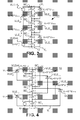
- FIG. 3 shows a realization corresponding to FIG. 2, in which six supercapacities SC 1 to SC 6 are connected in a series circuit 12 as memory elements.
- the voltage-limiting elements VLE 12 , VLE 23 , VLE 34 , VLE 45 and VLE 56 are formed as Z-diodes, wherein the voltage-limiting elements at the first and sixth memory element SC 1 and SC 6 are each formed as an integrated circuit VLEint 1 and VLEint 6 .
- the first supercapacitor SC 1 and the sixth supercapacitor SC 6 are each bridged with an integrated circuit with overvoltage protection function VLEint 1 and VLEint 6 , which has a threshold voltage of 2.5V.
- the integrated circuits VLEint 1 and VLEint 6 have a steeper characteristic than a Zener diode with 2.5 V breakdown voltage.
- FIG. 4 shows a further memory module 10 with six supercapacities SC 1 to SC 6 , which are interconnected in a series circuit 12.
- M 3 is selected.
- this memory module 10 has four combinations of supercapacities that are directly connected to one another. These are the supercapacitors SC 1 to SC 3 , which are bridged by a Zener diode VLE 123 having a breakdown voltage of about 7.5V.
- the combination, consisting of the supercapacitors SC 2 to SC 4 is bridged by a Zener diode VLE 234 , which also has a breakdown voltage of 7.5 V.
- next combination SC 3 to SC 5 is bridged with a Z-diode VLE 345 and the last 3-way combination, consisting of SC 4 to SC 6 , is also bridged with a Z-diode VLE 456 .
- these are each bridged with an integrated circuit VLEint 1 and VLEint 6 with overvoltage protection function, each having a threshold voltage of 2.5V.
- FIG. 5 shows a plurality of characteristic curves for Z-diodes. It can be clearly seen that Z-diodes with a breakdown voltage of more than 5 V have a significantly steeper characteristic than Z-diodes with a breakdown voltage below 5 V.
- FIG. 6 shows a further exemplary embodiment in which seven supercapacities are connected together in a series connection 12.
- Z-diodes VLE 1234 , VLE 2345 , VLE 3456 and VLE 4567 with a quadruple voltage of the maximum permissible voltage of a memory element can be used as the breakdown voltage for this overvoltage protection.
- the subcombination SC 1 and SC 2 and the subcombination SC 6 and SC 7 are each to be bridged with a voltage limiting element VLE 12 and VLE 67 .
- the bridge each having first and the seventh memory element SC 1 and SC 7 with a voltage-limiting element VLEint 1 and VLEint. 7
- the circuit arrangement according to the invention is advantageously suitable for use in a battery with maximum input voltage of 42V and minimum output voltage of 25V, with a lifetime of 15 years.
- Such a battery advantageously consists of several supercapacities, which is placed on a first PCB and covered by a second PCB become. Both PCBs have contact surface for the supercapacities and the corresponding component of the balancing circuit.
- a foam rubber cover is placed as a spring element, to exercise contact pressure.
- Two more metal or plastic lids Be on the top foam cover and under the bottom PCB introduced. All five covers have holes for bolts for vertical mounting which are contracted to provide enough contact pressure between the supercapacitors and the lower and upper PCBs.
Landscapes
- Engineering & Computer Science (AREA)
- Power Engineering (AREA)
- Emergency Protection Circuit Devices (AREA)
Abstract
Description
- Fig. 1
- eine Schaltungsanordnung mit Superkapazitäten und parallel geschalteten Z-Dioden gemäß dem Stand der Technik;
- Fig. 2
- eine schematische Schaltungsanordnung eines Speichermoduls gemäß der vorliegenden Erfindung;
- Fig. 3
- ein Schaltungsbeispiel mit Superkapazitäten und Z-Dioden als spannungsbegrenzende Elemente und M = 2;
- Fig. 4
- ein Schaltungsbeispiel mit Superkapazitäten und Z-Dioden und M = 3;
- Fig. 5
- verschiedene Kennlinien von Z-Dioden;
- Fig. 6
- eine schematische Schaltungsanordnung gemäß der vorliegenden Erfindung mit M = 4;
Claims (5)
- Schaltungsanordnung zur Begrenzung von Überspannungen bei aus Speicherelementen (SC) zusammengesetzten Speichermodulen (10), umfassend eine Reihenschaltung (12) aus n Speicherelementen (SCn), wobei die Reihenschaltung (12) zwischen ein erstes Potential (V1) und ein zweites Potential (V2) geschaltet ist und den n Speicherelementen (SCn) spannungsbegrenzende Elemente (VLE) zugeordnet sind, dadurch gekennzeichnet, dass M die maximale Anzahl von unmittelbar miteinander verbundenen Speicherelementen (SC) einer vorgegebenen Kombination ist, wobei für M ≥ 2 jeder Kombination ein spannungsbegrenzendes Element (VLE) parallel geschaltet ist und einem am ersten Potential (V1) angeschlossenen ersten Speicherelement (SC1) und einem am zweiten Potential (V2) angeschlossenen n-ten Speicherelement (SCn) jeweils ein spannungsbegrenzendes Element (VLE) parallel geschaltet ist und wobei für M > 2 jeder Unterkombination aus wenigstens 2 unmittelbar miteinander verbundenen Speicherelementen (SC) der Kombination, die ein am ersten Potential (V1) oder am zweiten Potential (V2) angeschlossenes Speicherelement (SC) aufweist, jeweils ein spannungsbegrenzendes Element (VLE) parallel geschaltet ist.
- Schaltungsanordnung nach Anspruch 1, dadurch gekennzeichnet, dass die Speicherelemente (SC) Superkapazitäten und/oder Akkumulatoren sind.
- Schaltungsanordnung nach Anspruch 1 oder 2, dadurch gekennzeichnet, dass die spannungsbegrenzenden Elemente (VLE) Z-Dioden sind.
- Schaltungsanordnung nach einem der Ansprüche 1 bis 3, dadurch gekennzeichnet, dass die spannungsbegrenzenden Elemente (VLE) jeweils die Spannung der ihnen parallel geschalteten Speicherelemente (SC) auf eine Spannung begrenzen, die sich aus der Summe der zulässigen Spannungen Umax der einzelnen Speicherelemente (SC) der jeweiligen Kombination oder Unterkombination ergibt.
- Schaltungsanordnung nach einem der Ansprüche 1 bis 4, dadurch gekennzeichnet, dass die spannungsbegrenzenden Elemente (VLE) für die Kombinationen Z-Dioden mit einer Durchbruchspannung von M*Umax sind und die spannungsbegrenzenden Elemente (VLE) für das erste Speicherelement (SC1) und das n-te Speicherelement (SCn) Z-Dioden mit einer Durchbruchspannung von Umax oder integrierte Schaltungen (VLEint) mit Überspannungsschutzfunktion sind und die spannungsbegrenzenden Elemente (VLE) für jede Unterkombination Z-Dioden mit einer Durchbruchspannung von K*Umax oder integrierte Schaltungen (VLEint) mit Überspannungsschutzfunktion sind, wobei K die Anzahl der Speicherelemente (SC) der Unterkombination ist.
Priority Applications (1)
| Application Number | Priority Date | Filing Date | Title |
|---|---|---|---|
| EP05105267A EP1610434A1 (de) | 2004-06-21 | 2005-06-15 | Schaltungsanordnung zur Begrenzung von Überspannungen bei Speichermodulen |
Applications Claiming Priority (3)
| Application Number | Priority Date | Filing Date | Title |
|---|---|---|---|
| EP04405381 | 2004-06-21 | ||
| EP04405381 | 2004-06-21 | ||
| EP05105267A EP1610434A1 (de) | 2004-06-21 | 2005-06-15 | Schaltungsanordnung zur Begrenzung von Überspannungen bei Speichermodulen |
Publications (1)
| Publication Number | Publication Date |
|---|---|
| EP1610434A1 true EP1610434A1 (de) | 2005-12-28 |
Family
ID=35456066
Family Applications (1)
| Application Number | Title | Priority Date | Filing Date |
|---|---|---|---|
| EP05105267A Withdrawn EP1610434A1 (de) | 2004-06-21 | 2005-06-15 | Schaltungsanordnung zur Begrenzung von Überspannungen bei Speichermodulen |
Country Status (1)
| Country | Link |
|---|---|
| EP (1) | EP1610434A1 (de) |
Cited By (2)
| Publication number | Priority date | Publication date | Assignee | Title |
|---|---|---|---|---|
| WO2008092756A3 (de) * | 2007-01-30 | 2008-10-02 | Bosch Gmbh Robert | Batterie mit z-dioden-spannungsbegrenzungsschaltung |
| EP4231492A1 (de) * | 2022-02-18 | 2023-08-23 | M&P Motion Control and Power Electronics GmbH | Überspannungsschutzsystem für energiespeicher |
Citations (5)
| Publication number | Priority date | Publication date | Assignee | Title |
|---|---|---|---|---|
| JPS61154083A (ja) * | 1984-12-26 | 1986-07-12 | Toshiba Corp | 太陽電池アレイ保護回路 |
| US4719401A (en) * | 1985-12-04 | 1988-01-12 | Powerplex Technologies, Inc. | Zener diode looping element for protecting a battery cell |
| EP0851445A2 (de) * | 1996-12-20 | 1998-07-01 | Asahi Glass Company Ltd. | Elektrischer Doppelschichtkondensator und Zellanordnungstyp-spezifische Energieversorgungseinrichtung |
| WO2001084574A1 (de) * | 2000-05-02 | 2001-11-08 | Abb Research Ltd. | Superkondensatoranordnung |
| DE10043139A1 (de) * | 2000-08-31 | 2002-03-28 | Ballard Power Systems | Überwachungsgerät für Brennstoffzellenspannungen |
-
2005
- 2005-06-15 EP EP05105267A patent/EP1610434A1/de not_active Withdrawn
Patent Citations (5)
| Publication number | Priority date | Publication date | Assignee | Title |
|---|---|---|---|---|
| JPS61154083A (ja) * | 1984-12-26 | 1986-07-12 | Toshiba Corp | 太陽電池アレイ保護回路 |
| US4719401A (en) * | 1985-12-04 | 1988-01-12 | Powerplex Technologies, Inc. | Zener diode looping element for protecting a battery cell |
| EP0851445A2 (de) * | 1996-12-20 | 1998-07-01 | Asahi Glass Company Ltd. | Elektrischer Doppelschichtkondensator und Zellanordnungstyp-spezifische Energieversorgungseinrichtung |
| WO2001084574A1 (de) * | 2000-05-02 | 2001-11-08 | Abb Research Ltd. | Superkondensatoranordnung |
| DE10043139A1 (de) * | 2000-08-31 | 2002-03-28 | Ballard Power Systems | Überwachungsgerät für Brennstoffzellenspannungen |
Non-Patent Citations (1)
| Title |
|---|
| PATENT ABSTRACTS OF JAPAN vol. 0103, no. 56 (E - 459) 29 November 1986 (1986-11-29) * |
Cited By (2)
| Publication number | Priority date | Publication date | Assignee | Title |
|---|---|---|---|---|
| WO2008092756A3 (de) * | 2007-01-30 | 2008-10-02 | Bosch Gmbh Robert | Batterie mit z-dioden-spannungsbegrenzungsschaltung |
| EP4231492A1 (de) * | 2022-02-18 | 2023-08-23 | M&P Motion Control and Power Electronics GmbH | Überspannungsschutzsystem für energiespeicher |
Similar Documents
| Publication | Publication Date | Title |
|---|---|---|
| EP2962380B1 (de) | Schaltungsanordnung zur inline-spannungsversorgung, verwendung einer solchen schaltungsanordnung und vorrichtung mit einer solchen schaltungsanordnung | |
| EP2145368B1 (de) | Schaltungsanordnung mit wenigstens zwei in serie geschalteten kondensatoren | |
| DE102022130515A1 (de) | Stromrichter, leistungssysteme und verfahren zum schutz von stromrichtern | |
| WO2015018748A1 (de) | Elektrische energiespeichervorrichtung und verfahren zum hochfahren der spannung an deren anschlüssen | |
| DE202011110740U1 (de) | Batterie mit mehreren Akkumulator-Zellen | |
| DE102014006772A1 (de) | Batteriesystem für ein Kraftfahrzeug mit zwei Spannungskreisen | |
| DE102011053013A1 (de) | Vorrichtung und Verfahren zur Symmetrierung der Spannungsaufteilung von in Reihe geschalteten Energiespeichern | |
| JP4463731B2 (ja) | エネルギー貯蔵モジュール中での過電圧を制限する回路構成 | |
| EP2051879B1 (de) | Verfahren zur lebensdauerverlängerung eines wiederaufladbaren energiespeichers | |
| EP0569351B1 (de) | Batterieladesystem mit fehleranzeige | |
| WO2008092756A2 (de) | Batterie mit z-dioden-spannungsbegrenzungsschaltung | |
| DE112017006121T5 (de) | Energieversorgungsvorrichtung, beleuchtungseinrichtung und verfahren zum herstellen einer energieversorgungsvorrichtung | |
| DE3422995C1 (de) | Überspannungsschutz-Schaltungsanordnung für Fernmelde-, insbesondere Fernsprechleitungen | |
| DE102021200924B4 (de) | Schaltungsanordnung mit zumindest einem Superkondensator und wenigstens einer Bypass-Schaltung, elektrischer Energiespeicher mit einer Schaltungsanordnung und Verwendung einer Schaltungsanordnung als Energiespeicher | |
| DE102020116814A1 (de) | Dämpfungsschaltung und stromrichter | |
| DE102017106770B4 (de) | Schaltungsanordnung zum Schutz vor Netzüberspannungen für Stromrichter von Fahrzeugen, insbesondere von fahrleitungsgebundenen Fahrzeugen | |
| DE102017206696A1 (de) | Batterie | |
| DE102018114641B4 (de) | Schaltung, Vorrichtung und Frequenzumrichter sowie Verfahren zum Betreiben einer elektronischen Schaltung | |
| DE10021315A1 (de) | Superkondensatoranordnung | |
| DE3045445A1 (de) | Schaltungsanordnung zur strom- und spannungsversorgung bei netzausfall | |
| EP4231492A1 (de) | Überspannungsschutzsystem für energiespeicher | |
| DE102022123386A1 (de) | Überspanungsschutzsystem für Energiespeicher | |
| DE102018108104A1 (de) | Photovoltaik-Stromversorgungsvorrichtung, insbesondere vom öffentlichen Stromnetz unabhängige Photovoltaik-Stromversorgungsvorrichtung, und hierfür geeignete Ladeschaltungsanordnung | |
| DE3634581C2 (de) | Statischer Verstärker für schwache Signale | |
| DE102006053810A1 (de) | Gleichrichter-Brückenschaltung mit Load-Dump-Schutz |
Legal Events
| Date | Code | Title | Description |
|---|---|---|---|
| PUAI | Public reference made under article 153(3) epc to a published international application that has entered the european phase |
Free format text: ORIGINAL CODE: 0009012 |
|
| AK | Designated contracting states |
Kind code of ref document: A1 Designated state(s): AT BE BG CH CY CZ DE DK EE ES FI FR GB GR HU IE IS IT LI LT LU MC NL PL PT RO SE SI SK TR |
|
| AX | Request for extension of the european patent |
Extension state: AL BA HR LV MK YU |
|
| 17P | Request for examination filed |
Effective date: 20060628 |
|
| AKX | Designation fees paid |
Designated state(s): AT CH DE FR GB LI NL |
|
| REG | Reference to a national code |
Ref country code: HK Ref legal event code: DE Ref document number: 1086953 Country of ref document: HK |
|
| STAA | Information on the status of an ep patent application or granted ep patent |
Free format text: STATUS: THE APPLICATION IS DEEMED TO BE WITHDRAWN |
|
| 18D | Application deemed to be withdrawn |
Effective date: 20120103 |
|
| RIN1 | Information on inventor provided before grant (corrected) |
Inventor name: GRUNDMANN, STEFFEN |
|
| REG | Reference to a national code |
Ref country code: HK Ref legal event code: WD Ref document number: 1086953 Country of ref document: HK |