The present invention also relates to a United States Patent Application No.
10/404,002 filed on 31 March 2003, a United States Patent Application No. 10/403,817
filed on 31 March 2003, an International Patent Application No. PCT/JP2004/001649
filed on 16 February 2004, and an International Patent Application No.
PCT/JP2004/001648 filed on 16 February 2004, which is incorporated herein by
reference.
BACKGROUND OF THE INVENTION
Field of the Invention
The present invention relates to a test emulator, a test module emulator, and a
record medium storing program therein. More particularly, the present invention
relates to a test emulator, a test module emulator, and a record medium storing program
therein for emulating test apparatuses including a plurality of exchangeable test modules
for supplying a test signal to DUTs respectively, and verifying a test environment
without using real things such as a DUT or a test module.
Description of Related Art
Conventionally, technologies are disclosed in Japanese patent application
publications No. 10-320229, No. 2000-267881, No. 2001-51025, No. 2001-134457, and
No. 2002-333469, as means for verifying test environment without using real things
such as a DUT or a test apparatus.
The Japanese patent application publications No. 10-320229 discloses: each
emulator unit for emulating function of each hardware unit of a semiconductor test
apparatus; a device emulator for emulating function of DUT; means for collecting data
required for execution of a test program from each of the emulator units based on a test
program; and an emulator including a device test emulator for generating a test signal in
a device emulator based on the collected data, comparing result signals from the device
emulator, and storing the result therein.
The Japanese patent application publication No.2000-267881 discloses a
semiconductor simulating apparatus for accurately simulating voltage and current which
change depending on internal resistance of the DUT.
The Japanese patent application publications No.2001-51025 discloses a
program debugging apparatus for a semiconductor test including: tester emulation
means for emulating operation of the semiconductor test apparatus; hardware
description language simulating means for simulating the DUT based on the hardware
description language; and debugging means for debugging the program for the
semiconductor test based on the simulating result of the DUT.
The Japanese patent application publications No. 2001-134457 discloses a
program debugging apparatus for a semiconductor test for composing data points
corresponding to each pin at high speed when emulating operation of the semiconductor
test apparatus.
The Japanese patent application publications No. 2002-333469 discloses a
program debugging apparatus for a semiconductor test for verifying program for the
semiconductor test being composed for a semiconductor device including an analogue
output terminal.
SUMMARY OF THE INVENTION
It is premised that the emulators of the test apparatuses described above are used
for the test apparatus having a proprietary architecture basically developed by a test
apparatus vendor. On the other hand, in test apparatuses in the future, a method for
constructing the test apparatus by combining modules developed by various vendors,
which is realized by an open architecture, is expected. Therefore, It is desirable to
offer an emulator for appropriately emulating the test apparatus constructed by the
various modules.
Therefore, it is an object of the present invention to provide a test emulator, a
test module emulator, and a record medium storing program therein which can solve the
foregoing problem. The above and other objects can be achieved by combinations
described in the independent claims. The dependent claims define further
advantageous and exemplary combinations of the present invention.
Therefore, according to the first aspect of the present invention, there is
provided a test emulator for emulating a test apparatus including a plurality of test
modules for supplying a test signal to devices under test respectively. The test
emulator includes: a plurality of test module emulation sections for emulating the
plurality of test modules generating the test signal based on different cycles; a control
emulation section for emulating a control apparatus for controlling the test of the
devices under test; a synchronous emulation section for generating test signal generating
timings, at which each of the plurality of test module emulation sections is to generate
the test signal in simulation corresponding to cycle time of the test module emulation
section, based on instructions from the control emulation section; a timing alignment
section for aligning the plurality of test signal generating timings generated by the
synchronous emulation section in order of time, and outputting them one by one; and a
schedule section for causing the test module emulation section corresponding to one of
the test signal generating timings output by the timing alignment section to generate the
test signal in simulation in the cycle time corresponding to the test signal generating
timing.
The test emulator may further include a device under test simulating section for
simulating operation of a device under test based on the test signal generated in
simulation.
The synchronous emulation section may further generate interruption collection
timings for collecting interruption to the control apparatus generated in simulation by
each of the plurality of test module emulation sections during the generation of the test
signal in the cycle time corresponding to the test signal generating timings, the timing
alignment section may align the plurality of test signal generating timings and the
plurality of interruption collection timings in order of time, and outputs them one by one,
and the schedule section may cause the test module emulation section corresponding to
the interruption collection timing to notify the control emulation section of the
interruption generated in simulation in the cycle time at which the test module
emulation section generates the test signal just before the interruption collection timing,
in case that the timing alignment section outputs one of the interruption collection
timings.
Each of the plurality of test module emulation sections may generate change
timing of the test signal in the cycle time at the generation of the test signal in the cycle
time corresponding to the test signal generating timing, and the test emulator may
further include a DUT connection section for acquiring the plurality of change timings
generated by the plurality of test module emulation sections, and for changing the test
signal in simulation one by one in order of time based on the plurality of change
timings.
The DUT connection section supplies the plurality of change timings acquired
from the plurality of test module emulation sections to the timing alignment section, the
timing alignment section may align the plurality of change timings, the plurality of test
signal generating timings, and the plurality of interruption collection timings in order of
time, and outputs them one by one, and the schedule section may cause the DUT
connection section to change the test signal in simulation at the change timing, in case
that the timing alignment section outputs one of the change timings.
Each of the plurality of the test module emulation sections may notify the
synchronous emulation section of the cycle end timing at which the cycle time ends
during the generation of the test signal in the cycle time corresponding to the test signal
generating timing, and the synchronous emulation section may generate the test signal
generating timings at which the test module emulation section generates the test signal
in simulation corresponding to next cycle time based on the cycle end timing notified
from each of the plurality of test module emulation sections.
The schedule section may cause the interruption generated in simulation by the
test module emulation section corresponding to the test signal generating timing to be
notified to the control emulation section during the generation of the test signal in the
cycle time just before the test signal generating timing, in case that the timing alignment
section outputs the test signal generating timing corresponding to the next cycle time.
Each of the plurality of test module emulation sections may be realized by
operating test module emulation program corresponding to the test module emulation
section by a computer, and the test module emulation program may include: a plurality
of hardware emulation functions, being provided corresponding to a plurality of
commands received by the test module from the control apparatus respectively, for
emulating operation of the test module corresponding to the command; and a control
function used in order for the schedule section to cause the test emulator to generate the
test signal in the cycle time corresponding to the test signal generating timing.
According to the second aspect of the present invention, there is provided a
record medium storing therein program for causing a computer to function as a test
emulator for emulating test apparatuses including a plurality of test modules for
supplying test signal to devices under test respectively. The program causes the
computer to function as: a plurality of test module emulation sections for emulating the
plurality of test modules generating the test signal based on different cycles; a control
emulation section for emulating a control apparatus for controlling the test of the
devices under test; a synchronous emulation section for generating test signal generating
timings, at which each of the plurality of test module emulation sections is to generate
the test signal in simulation corresponding to cycle time of the test module emulation
section, based on instructions from the control emulation section; a timing alignment
section for aligning the plurality of test signal generating timings generated by the
synchronous emulation section in order of time, and outputting them one by one; and a
schedule section for causing the test module emulation section corresponding to one of
the test signal generating timings output by the timing alignment section to generate the
test signal in simulation in the cycle time corresponding to the test signal generating
timing.
According to the third aspect of the present invention, there is provided a test
module emulator for emulating a test module among a plurality of test modules by a test
emulator for emulating test apparatuses including the plurality of test modules for
supplying test signal to devices under test respectively based on a different cycle. The
test emulator includes: a control emulation section for emulating a control apparatus for
controlling the test of the devices under test; a synchronous emulation section for
generating test signal generating timings, at which each of the plurality of test module
emulation sections is to generate the test signal in simulation corresponding to cycle
time of the test module emulation section, based on instructions from the control
emulation section; a timing alignment section for aligning the plurality of test signal
generating timings generated by the synchronous emulation section in order of time, and
outputting them one by one; and a schedule section for causing the test module
emulation section corresponding to one of the test signal generating timings output by
the timing alignment section to generate the test signal in simulation in the cycle time
corresponding to the test signal generating timing, and the test module emulator
includes a pattern generator emulation section for generating the test signal in
simulation in the cycle time corresponding to one of the test signal generating timings
based on instructions from the schedule section.
The test module emulator may further includes a test module interface emulation
section for notifying a synchronous emulation section of cycle end timing at which the
cycle corresponding to one of the test signal generating timings ends, and causing the
synchronous emulation section to further generate the test signal generating timing at
which the test module emulator is to generate the test signal in simulation for the next
time based on the cycle end timing.
According to the fourth aspect of the present invention, there is provided a
record medium storing therein program for causing a computer to function as a test
module emulator for emulating a test module among a plurality of test modules as for a
test emulator for emulating test apparatuses including the plurality of test modules for
supplying test signal to devices under test respectively based on a different cycle. The
test emulator includes: a control emulation section for emulating a control apparatus for
controlling the test of the devices under test; a synchronous emulation section for
generating test signal generating timings, at which each of the plurality of test module
emulation sections is to generate the test signal in simulation corresponding to cycle
time of the test module emulation section, based on instructions from the control
emulation section; a timing alignment section for aligning the plurality of test signal
generating timings generated by the synchronous emulation section in order of time, and
outputting them one by one; and a schedule section for causing the test module
emulation section corresponding to one of the test signal generating timings output by
the timing alignment section to generate the test signal in simulation in the cycle time
corresponding to the test signal generating timing, and the program causes the computer
to function as a pattern generator emulation section for generating the test signal in
simulation in the cycle time corresponding to one of the test signal generating timings
based on instructions from the schedule section.
According to the fifth aspect of the present invention, there is provided a test
apparatus including a test module for supplying a test signal to a device under test.
The test apparatus includes: a control apparatus for controlling a test of the device under
test; a test module for generating a test signal based on a cycle; and a test module
emulation section for emulating the test module. The control apparatus inputs an
instruction about which of a real test or a simulation test is to be selected for the test of
the device under test, the control apparatus supplies the test module with a test program
for testing the device under test and causes the test module to test the device under test
when the instruction indicates that the real test of the device under test is to be
performed, and the control apparatus supplies the test module emulation section with a
test program for testing the device under test and causes the test module emulation
section to simulate the test of the device under test when the instructions indicates that
the simulation test of the device under test is to be performed.
The control unit may execute communication software for performing
communication processing between the control unit and the test module, and the
communication software may decide whether the test program is to be supplied to the
test module or the test module emulation section based on the instructions included in
calling for initializing the communication software in cooperation with the control
apparatus.
According to the sixth aspect of the present invention, there is provided a test
emulator for emulating a test apparatus including a plurality of test modules for
supplying a test signal to devices under test. The test emulator includes: a plurality of
test module emulation sections for emulating the plurality of test modules generating
the test signal based on a cycle; a control emulation section for emulating a control
apparatus for controlling the test of the devices under test; and a schedule section for
scheduling test signal generating timing at which each of the plurality of test module
emulation sections is to generate test signal corresponding to a cycle time in simulation.
The test module emulation section outputs variation of voltage of the test signal during
the cycle time corresponding to the test signal generating timing by calling voltage
setting method of an output channel object which emulates an output channel for
multiple times on receiving the test signal generating timing by a function call, and the
test module emulation section notifies that output of the variation of the voltage of the
test signal corresponding to the cycle time is finished by calling an end method of the
output channel object output after the output of the variation of the voltage of the test
signal corresponding to the cycle time is finished.
The schedule section may calculate a period during which all of the test module
emulation sections finishes the output of the variation of the voltage of the test signal
based on the end method notified from each of the plurality of test module emulation
sections, and the test emulator may further comprise a device under test simulating
section for acquiring the test signal within the period and simulates operation of the
device under test during the period based on the test signal.
The output channel object may forbid the variation of the voltage in the period
during which the output of the variation of the voltage of the test signal was finished,
which was notified by the end method, after the end method was called.
The summary of the invention does not necessarily describe all necessary
features of the present invention. The present invention may also be a
sub-combination of the features described above.
BRIEF DESCRIPTION OF THE DRAWINGS
Fig. 1 is a block diagram showing a configuration of a test apparatus 10
according to an embodiment of the present invention.
Fig. 2 is a block diagram showing a functional configuration of a test emulator
190 according to an embodiment of the present invention.
Fig. 3 is a block diagram exemplary showing a hardware configuration of a
computer 20 according to an embodiment of the present invention.
Fig. 4 is a block diagram showing a functional configuration of a test module
emulation section 270 according to an embodiment of the present invention.
Fig. 5 shows an example of a class hierarchical structure 500 according to an
embodiment of the present invention.
Fig. 6 is a flow chart showing a test signal generating processing flow of the test
emulator 190 according to an embodiment of the present invention.
Fig. 7 is a drawing exemplary showing the test signal simulated by the test
emulator 190 according to an embodiment of the present invention.
Fig. 8 illustrates software architecture according to an embodiment of the
present invention.
Fig. 9 illustrates the use of test classes according to an embodiment of the
invention.
Fig. 10 is a Unified Modelling Language (UML) diagram illustrating the
interaction of a tester system and different vendor-supplied module resources according
to an embodiment of the invention.
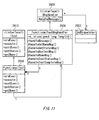
Fig. 11 illustrates an embodiment of site controller objects for managing a user's
test as maintained by a site controller.
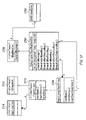
Fig. 12 illustrates an embodiment of an object surrogate at the system controller
side that represents the site controller object shown in Figure 11.
Fig. 13 illustrates a test environment according to an embodiment of the
invention.
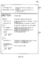
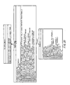
Fig. 14 illustrates an example of a simulation configuration file according to an
embodiment of the present invention.
Fig. 15 illustrates another example of the simulation configuration file according
to an embodiment of the present invention.
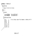
Fig. 16 illustrates an example of an offline configuration file according to an
embodiment of the present invention.
Fig. 17 illustrates another example of the offline configuration file according to
an embodiment of the present invention.
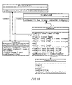
Fig. 18 illustrates an example of a class hierarchical structure 5200 according to
an embodiment of the present invention.
Fig. 19 illustrates a specification diagram of a channel object according to an
embodiment of the present invention.
Fig. 20 illustrates a specification diagram of an event object according to an
embodiment of the present invention.
Fig. 21 illustrates an example of a base class of the digital module according to
an embodiment of the present invention.
Fig. 22 illustrates an example of class declaration of the digital driver module
according to an embodiment of the present invention.
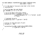
Fig. 23 illustrates an example of a handleEvent method of the digital driver
module according to an embodiment of the present invention.
Fig. 24 illustrates class declaration of the digital strobe module according to an
embodiment of the present invention.
Fig. 25 illustrates an example of a handleEvent method of the digital strobe
module according to an embodiment of the present invention.
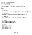
Fig. 26 illustrates an example of a class definition of a DUT model according to
an embodiment of the present invention.
Fig. 27 illustrates an example of a run method of the DUT model according to
an embodiment of the present invention.
Figs. 28A and 28B illustrate positioning of a system bus access library 6014 in
real environment 6000 and emulation environment 6050.
DETAILED DESCRIPTION OF THE INVENTION
The invention will now be described based on the preferred embodiments,
which do not intend to limit the scope of the present invention, but exemplify the
invention. All of the features and the combinations thereof described in the
embodiment are not necessarily essential to the invention.
Fig. 1 is a block diagram showing a configuration of a test apparatus 10
according to an embodiment of the present invention. The test apparatus 10 generates
a test signal, supplies it to a DUT 100 (Device Under Test), and judges acceptability of
the DUT 100 based on whether a result signal, which is output from the DUT 100 as a
result of the DUT 100 being operated based on the test signal, coincides with an
expected value. The test apparatus 10 according to the present embodiment is realized
by an open architecture, and various kinds of modules based on the open architecture
are used as a test module 170 and the like for supplying the test signal to the DUT 100.
Moreover, the test apparatus 10 includes a test emulator 190 for emulating a real test of
the DUT 1000, and the test emulator 190 provides an emulation environment for
appropriately changing a configuration in response to the change of the test module 170
and the like used for the real test, and for appropriately emulating the real test of the
DUT 1000.
The test apparatus 10 includes a system controller 110, a telecommunication
network 120, site controllers 130a-130c, a bus switch 140, synchronous modules
150a-150b, synchronous connection modules 160a-160b, the test modules 170a-170b, a
load board 180, and the test emulator 190. The test apparatus 10 connects with the
DUTs 100a-100b.
The system controller 110 receives and stores test control program, test program,
test data and the like, which is used for the test of the DUTs 100a-100b by the test
apparatus 10, through an external network or the like. The telecommunication
network 120 connects the system controller 110, the site controllers 130a-130c, and the
test emulator 190, and relays communication between them.
The site controllers 130a-130c are examples of the control apparatus according
to the present invention, and control the test of the DUTs 100. Here, each of the
plurality of site controllers 130 controls the test of one of the DUTs 100 respectively.
For example, in Fig. 1, the site controller 130a controls the test of the DUT 100a, and
the site controller 130b controls the test of the DUT 100b. Alternatively, the plurality
of site controllers 130 control the test of the plurality of DUTs 100 respectively.
More specifically, the site controller 130 acquires the test control program from
the system controller 110 through the telecommunication network 120 and executes it.
Next, based on the test control program, the site controller 130 acquires the test program
and the test data used for the test of the DUT 100 from the system controller 110, and
stores them in a module, such as the synchronous modules 150 or one or a plurality of
the test module 170, which is used for the test of the DUT 100, through the bus switch
140. Next, the site controller 130 instructs the start of the test to the synchronous
module 150 through the bus switch 140 based on the test program and the test data.
Then, the site controller 130 receives an interruption, which indicates that the test is
completed, from, for example, the synchronous module 150, and causes each of the
modules to perform the next test based on the test result.
The bus switch 140 connects each of the plurality of site controllers 130 to the
synchronous modules 150 and one or a plurality of the test modules 170 which are
controlled by the site controller 130, and relays the communication between them.
Here, a predetermined site controller 130 sets up the bus switch 140 in order to connect
each of the plurality of site controllers 130 with the synchronous module 150 and one or
a plurality of the test modules 170 used by the site controller 130 for the test of the DUT
100, based on the instruction of a user of the test apparatus 10, the test control program,
etc. For example, in Fig. 1, the site controller 130a is set up so that it connects with
the synchronous module 150a and the plurality of test modules 170a, thereby the DUT
100a is tested. Moreover, the site controller 130b is set up so that it connects with the
synchronous module 150b and the plurality of test modules 170b, thereby the DUT
100b is tested.
Here, since configuration and operation of the site controller 130b for testing the
DUT 100b using the synchronous module 150b, the synchronous connection modules
160b and one or a plurality of the test module 170b are substantially the same as
configuration and operation of the site controller 130a for testing the DUT 100a using
the synchronous module 150a, the synchronous connection modules 160a and one or a
plurality of the test module 170a, the configuration and the operation of the site
controller 130a for testing the DUT 100a will be mainly described hereinafter unless
there is no difference.
The synchronous module 150a generates a test signal generating timing, at
which the plurality of test modules 170 used for the test of the DUT 100a are to
generate the test signal, based on the instruction of the site controller 130a. Moreover,
the synchronous module 150a receives the test result from one or a plurality of the test
modules 170a through the synchronous connection module 160a, and causes one or a
plurality of the test module 170a to perform sequence of the test program according to
the acceptability of the test result.
The synchronous connection module 160a notifies the test module 170a of the
test signal generating timing generated by the synchronous module 150a, where the test
module 170a is to be operated corresponding to the test signal generating timing. Then,
the synchronous connection module 160a causes each of one or a plurality of the test
modules 170a to operate at a predetermined timing. Moreover, the synchronous
connection module 160a receives the test result from one or a plurality of the test
modules 170a, and transmits it to the synchronous module 150a.
The plurality of test modules 170a connect with a part of a plurality of terminals
of the 100a respectively, and tests the DUT 100a based on the test program and the test
data stored in the site controller 130a. During the test of the DUT 100a, test module
170a generates the test signal from the test data based on the sequence defined by the
test program, and supplies the test signal to the terminals of the DUT 100a connected to
the test modules 170a. Next, test module 170a acquires the result signal, which is
output as a result of the DUT 100a being operated based on the test signal, and the
result signal is compared with an expected value. Then, the test module 170a
transmits the comparison result of the result signal and the expected value to the
synchronous connection module 160a as the test result. Here, the plurality of test
modules 170a generate the test signal based on different cycles in order to change the
cycle of the test signal dynamically based on the test program and the test data.
Moreover, the test module 170a generates an interruption to the site controller
130a, when the processing of the test program is completed, or when an abnormality
occurs during the execution of the test program. This interruption is notified to the site
controller 130a corresponding to the test module 170a through the bus switch 140, and
interruption processing is performed by the processor of the site controller 130a.
The plurality of DUTs 100 are mounted on the load board 180, by which the
plurality of test modules 170 and the corresponding terminals of the DUTs 100 are
connected.
The test emulator 190 emulates the test apparatus 10 based on the test control
program, the test program, and the test data stored in the system controller 110. Then,
the test emulator 190 simulates the test of the DUT 100 using the simulation model of
the DUT 100. In the present embodiment, the test emulator 190 simulates the
operation of the site controller 130, the synchronous module 150 and the synchronous
connection modules 160 and one or a plurality of the test modules 170 controlled by the
site controller 130, and the DUT 100 which is to be tested by the corresponding site
controller 130. By using the test emulator 190, the user of the test apparatus 10 starts
the verification of the test control program, the test program, and/or the test data prior to
the preparation of the DUT 100, the synchronous module 150, the synchronous
connection module 160, the test module 170, etc. Moreover, by providing the plurality
of test emulators 190, the test control program, the test program, and/or the test data are
developed, without each of the plurality of users occupying the expensive real test
environment.
As stated above, the test apparatus 10 is realized by an open architecture and
various kinds of modules, which fulfil the specification of the open architecture, are
utilized. Then, the test apparatus 10 is used by inserting the modules, such as the
synchronous module 150, the synchronous connection module 160, and the test module
170, into arbitrary connection slots of the bus switch 140. At this time, the user of the
test apparatus 10 etc. changes topology of the bus switch 140 through the site controller
130a for example, causes the plurality of modules used for the test of the DUT 100 to
connect with the site controller 130 for controlling the test of the DUT 100. Thereby,
the user of the test apparatus 10 selects a suitable module according to the number of
the terminals, the arrangement of the terminals, the kind of the terminals, or the kind of
the test for each of the plurality of the DUTs 100, and mounts the module on the test
apparatus 10.
Alternatively, as a substitution for the above-mentioned example, the
synchronous connection module 160a and the synchronous connection module 160b are
realized by a synchronous connection section provided for all of the test modules 170
used for the test apparatus 10. In this case, the user of the test apparatus 10 etc. selects
a suitable module according to the property of the plurality of DUTs 100 by changing
the topology of the synchronous connection section and the test module 170 with the
change of the topology of the bus switch 140.
Fig. 2 is a block diagram showing a functional configuration of the test emulator
190 according to the embodiment of the present invention. The test emulator 190
includes a site control emulation section 230, a bus switch emulation section 240, a
synchronous module emulation section 250, a synchronous connection module
emulation section 260, one or a plurality of test module emulation sections 270, a DUT
connection section 280, a DUT simulating section 200, and a schedule control section
275. Hereinafter, a case where the test emulator 190 emulates the test of the DUT
100a by the site controller 130a will be explained.
The site control emulation section 230 emulates the site controller 130a
illustrated in Fig. 1. That is, the site control emulation section 230 acquires the test
control program from the system controller 110 through the telecommunication network
120 and executes it. Next, the site control emulation section 230 acquires the test
program and the test data, which are used for the test of the DUT 100a based on the test
control program, from the system controller 110, and stores them in module emulation
sections such as the synchronous module emulation section 250 or one or a plurality of
the test module emulation sections 270 through the bus switch emulation section 240.
Here, the site control emulation section 230 issues simulation commands, such
as read-out access and write-in access from/to a storage area in the module, to the bus
switch emulation section 240, where real commands are to be issued by the site
controller 130a to the synchronous modules 150a and one or a plurality of the test
modules 170a. The site control emulation section 230 stores the test program and the
test data in the synchronous module emulation sections 250, one or a plurality of the test
module emulation sections 270, etc. through the bus switch emulation section 240 by
issuing the write-in access of the test program and the test data in simulation to the bus
switch emulation section 240.
Moreover, the site control emulation section 230 receives the interruption
simulated by the synchronous module emulation section 250 and the test module
emulation section 270 through the bus switch emulation section 240, and simulates the
interruption processing of the site controller 130a.
The bus switch emulation section 240 emulates the bus switch 140 illustrated in
Fig. 1, and relays the communication between the site control emulation section 230,
and the synchronous module emulation sections 250 and one or a plurality of the test
module emulation sections 270.
The synchronous module emulation section 250 emulates the synchronous
module 150 illustrated in Fig. 1, and generates the test signal generating timing, at
which each of the plurality of test module emulation sections 270 is to generate the test
signal in simulation corresponding to the cycle time of the test module emulation
section 270, based on the instructions from the site control emulation section 230.
Next, the synchronous module emulation section 250 receives cycle end timing, which
is the end timing of the cycle time, from the test module emulation section 270 which
generates the test signal. Then, according to the cycle end timing, the synchronous
module emulation section 250 generates: a test signal generating timing at which the
test module emulation section 270 is to generate the next test signal; a test result
collection timing for collecting the test results from the test module emulation section
270; a cycle termination timing for causing the test module emulation section 270 to
terminate the processing of the cycle time; and an interruption collection timing for
collecting the interruption to the site control emulation section 230 from the test module
emulation section 270. Here, the interruption to the site control emulation section 230
from the test module emulation section 270 is the simulated interruption generated by
each of the plurality of test module emulation sections 270 for the site controller 130a
during the generation of the test signal in the cycle time corresponding to the test signal
generating timing.
The synchronous connection module emulation section 260 emulates the
synchronous connection module 160 illustrated in Fig. 1, and notifies the schedule
control section 275 of the test signal generating timing generated by the synchronous
module emulation section 250 in simulation, the test result collection timing and the
cycle termination timing and the interruption collection timing which are generated by
the synchronous module emulation section 250 for the emulation. Moreover, the
synchronous connection module emulation section 260 receives the test result from one
or a plurality of the test module emulation sections 270, and transmits it to the
synchronous module emulation section 250.
The test module emulation section 270 receives instruction of a cycle start from
the synchronous module emulation section 250 which received instructions of a test
signal generation, and generates the test signal in simulation in the cycle time
corresponding to the test signal generating timing based on the test program and the test
data stored in the site control emulation section 230. More specifically, the test
module emulation section 270 generates a change timing of the test signal in simulation
in the cycle time during the generation of the test signal in the cycle time corresponding
to the test signal generating timing. Alternatively, the test module emulation section
270 generates change timings corresponding to a cycle time as a change timing of the
test signal, where the number of the change timings is defined by specification of the
test module 170 corresponding to the test module emulation section 270. Moreover,
the test module emulation section 270 acquires the output signal output as a result of the
DUT simulating section 200 being operated in simulation based on the test signal, and
compares the result with the expected value defined based on the test program and the
test data. Then, the test module emulation section 270 transmits the comparison result
of the result signal and the expected value to the synchronous module emulation section
250 through the synchronous connection module emulation section 260 as the test
result.
Moreover, in response to instruction of the interruption from the schedule
section 277, the test module emulation section 270 notifies the site control emulation
section 230 through the bus switch emulation section 240 of the interruption generated
in simulation in the cycle time during which the last test signal before receiving the
instruction of the interruption is generated.
The DUT connection section 280 acquires the plurality of change timings
generated by the plurality of test module emulation sections 270, and changes the test
signal in simulation in order of time based on the plurality of change timings.
The DUT simulating section 200 simulates operation of the DUT 100 described
by hardware description languages, such as Verilog-HDL or VHDL, based on the test
signal acquired from the DUT connection section 280. Then, the DUT simulating
section 200 generates a result signal by the simulation, which is output as a result of the
DUT 100 being operated based on the test signal, and supply it to the test module
emulation section 270 through the DUT connection section 280.
The schedule control section 275 controls the schedule which operates each of
the module emulation sections based on various kinds of timings generated by the
plurality of module emulation sections in the simulated test of the DUT 100 by the
synchronous module emulation section 250, the synchronous connection module
emulation section 260, the plurality of test module emulation sections 270, and the DUT
connection section 280. The schedule control section 275 includes a timing alignment
section 276 and a schedule section 277.
The
timing alignment section 276 aligns the plurality of test signal generating
timings, the plurality of interruption collection timings, the plurality of cycle
termination timings and the plurality of test result collection timings, which are
generated by the synchronous
module emulation section 250, and the plurality of
change timings that are generated by one or a plurality of the test
module emulation
sections 270 and are supplied by the
DUT connection section 280, in order of time.
Then, the
timing alignment section 276 outputs these aligned timings to the
schedule
section 277 one by one. The
schedule section 277 notifies the module emulation
section and the
DUT connection section 280 corresponding to the timings of each of the
timings output from the
timing alignment section 276 one by one. Then, the
schedule
section 277 causes the module emulation section or the
DUT connection section 280 to
perform the operation corresponding to the timings. The operation of the
schedule
section 277 according to the kind of the timing output from the
timing alignment section
276 will be explained hereinafter.
The schedule section 277 notifies the synchronous module emulation section 250 of the
test signal generating timing, and instructs the generation of the test signal by the test
module emulation section 270 corresponding to the test signal generating timing
through the synchronous module emulation section 250. Thereby, the schedule section
277 causes the test module emulation section 270 corresponding to the test signal
generating timing to generate the test signal in simulation in the cycle time
corresponding to the test signal generating timing through the synchronous module
emulation section 250. (2) In case that the timing alignment section 276 outputs the interruption
collection timing
The schedule section 277 instructs the generation of the interruption to the test module
emulation section 270 which is designated corresponding to the interruption collection
timing. Thereby, the schedule section 277 causes the test module emulation section
270 to notify the site control emulation section 230 through the bus switch emulation
section 240 of the interruption generated in simulation in the cycle time during which
the test signal is generated just before the interruption collection timing. (3) In case that the timing alignment section 276 outputs the cycle
termination timing
The schedule section 277 notifies the test module emulation section 270 corresponding
to the cycle termination timing that the cycle end timing has come. (4) In case that the timing alignment section 276 outputs the test result
collection timing
The schedule section 277 notifies the test module emulation section 270 corresponding
to the test result collection timing that the test result collection timing has come. In
response, the test module emulation section 270 notifies the synchronous module
emulation section 250 through the synchronous connection module emulation section
260 of the comparison result of the result signal and the expected value in the cycle
time. (5) In case that the timing alignment section 276 outputs the change timing
The DUT connection section 280 supplies the plurality of change timing acquired from
the plurality of test module emulation sections 270 to the timing alignment section 276.
In response, the timing alignment section 276 aligns the plurality of change timings and
other various timings altogether in order of time.
If the timing alignment section 276 outputs the change timing, the schedule
section 277 notifies the DUT connection section 280 that the change timing has come,
in order to change the test signal in simulation at the change timing. In response, the
DUT connection section 280 changes the test signal in simulation at the change timing.
Here, the test module emulation section 270 notifies the schedule control section
275 of result signal acquisition timing, which is a timing of the acquisition of the result
signal. Then, the timing alignment section 276 aligns the result signal acquisition
timing and the other various timings in order of time. In this case, when the timing
alignment section 276 outputs the result signal acquisition timing, the schedule section
277 causes the DUT connection section 280 to supply the result signal to the test
module emulation section 270 which is to acquire the result signal at the result signal
acquisition timing.
Moreover, the DUT connection section 280 acquires the plurality of change
timings generated by the plurality of test module emulation sections 270, and supplies
them to the DUT simulating section 200, without aligning them in order of time. In
this case, the DUT simulating section 200 aligns the plurality of supplied change
timings in order of time, and performs the simulation of the DUT 100 based on a
plurality of aligned change timings.
According to the test emulator 190 described above, by providing the
synchronous module emulation section 250, the synchronous connection module
emulation section 260 and one or a plurality of the test module emulation sections 270
respectively corresponding to the synchronous module 150, the synchronous connection
modules 160 and one or a plurality of the test modules 170 of the real system of the test
apparatus 10, the module emulation sections can be easily replaced as other module
emulation sections. Thereby, in case that one module is replaced as another modules
in the real system of the test apparatus 10, in the test emulator 190, a module emulation
section corresponding to the module is replaced by a module emulation section
corresponding to the other module. Then substantially the same test environment as
the real system of the test apparatus 10 is provided on the test emulator 190.
Alternatively, as a substitution for the above-mentioned example, the site
control emulation section 230, the bus switch emulation section 240, the synchronous
module emulation section 250, the test module emulation section 270, the schedule
control section 275, the DUT connection section 280, and the DUT simulating section
200 are realized by a distributed system including a plurality of computers.
Fig. 3 is a block diagram exemplary showing a hardware configuration of the
test emulator 190 according to the present embodiment of the invention. The test
emulator 190 according to the present embodiment is realized by a computer 20 which
includes CPU 300, ROM 310, RAM 320, a communication interface 330, a hard disk
drive 340, a flexible disk drive 350, and a CD-ROM drive 360.
The CPU 300 operates based on the program stored in the ROM 310 and the
RAM 320, and controls each part. The ROM 310 stores boot program which the CPU
300 executes during start up of a computer 20, program depending on the hardware of
the computer 20 and the like. The RAM 320 stores program which the CPU 300
executes, data which the CPU 300 uses. The communication interface 330
communicates with other equipments through a telecommunication network. The hard
disk drive 340 stores the program and the data which the computer 20 uses, and supplies
them to the CPU 300 through the RAM 320. The flexible disk drive 350 reads
program or data in a flexible disk 390, and provides them to the RAM 320. The
CD-ROM drive 360 reads program or data in a CD-ROM 395, and provides them to the
RAM 320.
The program provided to the CPU 300 through the RAM 320 is stored in a
record medium, such as the flexible disk 390, the CD-ROM 395, or an IC card, which is
provided by a user. The program is read from the record medium, installed in the
computer 20 through the RAM 320, and executed by the computer 20.
The program modules, which are installed and executed in/by the computer 20
and causes the computer 20 to function as the test emulator 190, includes a DUT
simulating module, a site control emulation module, a bus switch emulation module, a
synchronous module emulation module, a synchronous connection module emulation
module, a test module emulation module, a schedule control module, a timing alignment
module, a schedule module, and a DUT connection module. The programs or the
modules causes the computer 20 to function as the DUT simulating section 200, the site
control emulation section 230, the bus switch emulation section 240, the synchronous
module emulation section 250, the synchronous connection module emulation section
260, the test module emulation section 270, the schedule control section 275, the timing
alignment section 276, the schedule section 277, and the DUT connection section 280
respectively.
Alternatively, the programs or the modules described above are stored in an
external record medium. It is possible to use an optical record medium such as DVD
or PD, a magneto-optical record medium such as Minidisk, a tape medium, a magnetic
record medium or a semiconductor memory such as an IC card as a record medium
instead of the flexible disk 390 and the CD-ROM 395. Moreover, a storage device,
such as a hard disk or RAM in a server system on a dedicated telecommunication
network or the Internet, is used as a record medium and the program may be provided to
the computer 20 via the telecommunication network.
Fig. 4 is a block diagram showing a functional configuration of the test module
emulation section 270 according to the embodiment of the present invention. In Fig. 4,
the test module emulation section 270 is realized by operating the test module emulation
program or test module emulation module corresponding to the test module emulation
section 270 by the computer 20.
The test module emulation section 270 includes a plurality of hardware
emulation functions provided corresponding to each of the plurality of commands
received by the test module 170 through the bus switch 140 from the site controller 130,
and a control function called in order to notify the test module emulation section 270 of
various kinds of timings. The test module emulation section 270 operates in response
to the call to these functions from the bus switch emulation section 240 and the schedule
control section 275. Here, the control function is used in order for the schedule control
section 275 to order the generation of the test signal in simulation in the cycle time
corresponding to the test signal generating timing, and to order to notify the site control
emulation section 230 of the interruption generated in simulation in the cycle time when
the test module emulation section 270 generates the test signal just before the
interruption collection timing.
The test module emulation section 270 includes a test module IF emulation
section 400 (test module interface emulation section), a pattern generator emulation
section 430, a waveform shaper emulation section 440, a pin control emulation section
450, and a parameter measurement emulation section 460.
The test module IF emulation section 400 is started-up when the hardware
emulation function is called from the bus switch emulation section 240, and when the
control function is called from the schedule control section 275. The test module IF
emulation section 400 controls the operation of the test module emulation section 270
corresponding to these function calling. The test module IF emulation section 400
includes a machine word DB 420 and a control function processing section 410.
The machine word DB 420 emulates a storage area stored in the storage area
provided in the test module 170. When the machine word DB 420 receives a
command from the site control emulation section 230 in simulation through the bus
switch emulation section 240 by the calling of the hardware emulation function, it
accesses the storage area in the machine word DB 420 corresponding to the command.
More specifically, the test module IF emulation section 400 according to the
present embodiment stores a plurality of hardware emulation functions for emulating
the operation of the test module emulation section 270 corresponding to a plurality of
commands, such as read-out access and write-in access, respectively. When the
read-out access is received from the site control emulation section 230 through the bus
switch emulation section 240, the test module IF emulation section 400 replies the data
in the machine word DB 420 corresponding to the storage area for the read-out access,
to the site control emulation section 230 through the bus switch emulation section 240.
Moreover, when the machine word DB 420 receives the write-in access, it stores the
data to be written in the storage area of the machine word DB 420 corresponding to the
storage area for the write-in access. For example, when the machine word DB 420
receives the write-in access of the test program or the test data from the site control
emulation section 230 through the bus switch emulation section 240, it stores the test
programs or the test data in the storage area of the machine word DB 420 corresponding
to the write-in access.
When the control function processing section 410 receives the control function
call from the schedule control section 275, the control function processing section 410
causes the pattern generator emulation section 430, the waveform shaper emulation
section 440, the pin control emulation section 450, and the parameter measurement
emulation section 460 to emulate the operation of the test module 170 according to the
control function in response to the instruction of the control function. More
specifically, when the schedule control section 275 instructs the generation of the test
signal using the control function in the cycle time corresponding to the test signal
generating timing, the control function processing section 410 reads a part of the
program and a part of the data among the test program and the test data stored in the
machine word DB 420, where the part of the program and the data are to be processed
by the test module emulation section 270 during the cycle time. Then, the control
function processing section 410 causes the pattern generator emulation section 430, the
waveform shaper emulation section 440, the pin control emulation section 450, and the
parameter measurement emulation section 460 to perform the processing corresponding
to the part of the program and the part of the data.
The pattern generator emulation section 430 emulates the pattern generator of
the test module 170. That is, the pattern generator emulation section 430 receives the
test program and the test data stored in the machine word DB 420 from the control
function processing section 410 by the function call, for example. Then the instruction,
which indicates that the test signal is to be generated for a certain cycle time, is received
from the schedule control section 275 by the function call through the control function
processing section 410, and the test signal, which is to be generated in the cycle time, is
generated in simulation.
Moreover, the pattern generator emulation section 430 acquires the result signal
through the DUT connection section 280 and the waveform shaper emulation section
440, which is output in simulation as a result of the DUT simulating section 200 being
operated based on the test signal, and the result signal is compared with the expected
value.
The waveform shaper emulation section 440 emulates the waveform shaper of
the test module 170. That is, the waveform shaper emulation section 440 shapes the
waveform of the test signal in simulation in response to the test signal from the pattern
generator emulation section 430. Then the waveform is output to the DUT connection
section 280.
The pin control emulation section 450 emulates the pin control section of the
test module 170. That is, the pin control emulation section 450 sets parameters, such
as operating voltage, for each terminal from which the test signal is output in simulation
by the waveform shaper emulation section 440 and/or the parameter measurement
emulation section 460 based on the test program.
The parameter measurement emulation section 460 emulates the parameter
measurement section of the test module 170. That is, for example, the parameter
measurement emulation section 460 receives an instruction of a direct current test (DC
parametric test) from the schedule control section 275 through the control function
processing section 410 by the function call, and generates the test signal in simulation,
which is to be generated in the cycle time of the direct current test. Moreover, the
parameter measurement emulation section 460 acquires the result signal, which is
output in simulation as a result of the DUT simulating section 200 being operated based
on the test signal in the direct current test.
Moreover, in case that the test module emulation section 270 generates the test
signal in the cycle time corresponding to the test signal generating timing, the control
function processing section 410 notifies the synchronous module emulation section 250
of the cycle end timing at which the cycle, which corresponds to the test signal
generating timing, ends.
As stated above, the control function processing section 410 notifies the
synchronous module emulation section 250 through the schedule control section 275 of
the cycle end timing at which the cycle ends in the generation of the test signal in the
cycle time corresponding to the test signal generating timing. Thereby, the control
function processing section 410 causes the synchronous module emulation section 250
to further generate the test signal generating timing at which the test module emulation
section 270 is to generate the test signal in simulation for the next time based on the
cycle end timing.
Moreover, when the control function processing section 410 receives the
instruction of the interruption generation from the schedule control section 275, the
control function processing section 410 transmits the instruction of the interruption
generation to the pattern generator emulation section 430, the waveform shaper
emulation section 440, and the pin control emulation section 450 by the function call,
for example. The pattern generator emulation section 430, the waveform shaper
emulation section 440, and the pin control emulation section 450, which receive the
instruction of the interruption generation, notify the control function processing section
410 of the interruption generated in simulation in the cycle time just before the
interruption collection timing among the cycle times during which the test module
emulation section 270 generates the test signal. When the interruption is notified, the
control function processing section 410 notifies the site control emulation section 230 of
the interruption through the bus switch emulation section 240 by calling the hardware
emulation function for the notification of the interruption included in the bus switch
emulation section 240, for example.
Fig. 5 shows an example of a class hierarchical structure 500 according to the
embodiment of the present invention. In the present embodiment, module emulation
program, which realizes the module emulation sections such as the synchronous module
emulation section 250, the synchronous connection module emulation section 260, and
the test module emulation section 270, is created using class functions, which are
frameworks of the module emulation program defined in order to realize the open
architecture of the test apparatus 10 in simulation.
The simulation component class 510 is a class which defines rules for calling a
plurality of parameters, return values and etc. of method functions, which are to be
included in the module emulation program, with a virtual method function. The
simulation component class 510 includes a plurality of virtual hardware emulation
functions 512 and a plurality of virtual control functions 514.
Here, read() is a method function for emulating the operation of the module
corresponding to the read-out access which is called when the site control emulation
section 230 issues the read-out access command in simulation. write() is a method
function for emulating operation of the module corresponding to the write-in access
which is called when the site control emulation section 230 issues the write-in access
command in simulation. setBaseAddress() is a method function which is called when
the site control emulation section 230 issues in simulation the base address setting
command, which is issued by the site controller 130 when the base address of the
storage area of the test module 170 is set up.
registerEvent() is a method function which is called when the synchronous
connection module emulation section 260, the test module emulation section 270, and
the DUT connection section 280, which receive the notices from the synchronous
module emulation section 250, notify the timing alignment section 276 of the
interruption collection timing, the change timing, the result signal acquisition timing,
etc. and register the timings to the timing alignment section 276. handleEvent() is a
method function which is called by the schedule control section 275, in order to cause
the synchronous module emulation section 250, the synchronous connection module
emulation section 260, the test module emulation section 270, and the DUT connection
section 280 to perform the processing in response to the timings when the test signal
generating timing, the interruption collection timing, the change timing, the result signal
acquisition timing, etc. have come. raiseEvent() is a method function which is called
when the synchronous module emulation section 250, the synchronous connection
module emulation section 260, the test module emulation section 270, and the DUT
connection section 280 notify the schedule control section 275 of an event which is to
be processed asynchronously without regard to the timings.
A Company A's module class 520 and a Company B's module class 530 are
classes derived from the simulation component class 510, i.e., module emulation
programs, which are supplied by manufacturers of the modules for example, for
emulating common function included in the modules of the manufacturers in common.
The Company A's module class 520 and the Company B's module class 530 include a
plurality of real hardware emulation functions 522 and a plurality of real control
functions 524 respectively. Each of the plurality of real hardware emulation functions
522 and the plurality of real control functions 524 are module emulation programs
which are described corresponding to the plurality of virtual hardware emulation
functions 512 and the plurality of virtual control functions 514 respectively, and
describe the contents of the processing of the real method functions (non-virtual method
functions) corresponding to the virtual method functions.
The Company A's module class 520 and the Company B's module class 530
include classes which are further derived. For example, in Fig. 5, the Company B's
module class 530 is further derived in a digital test module class 540, a power source
module class 560, and a synchronous module class 590.
The digital test module class 540 is a class of test module emulation program for
emulating the test module 170 for performing the functional test of the DUT 100. The
digital test module class 540 is further derived in a 250 MHz digital test module class
550 for emulating the test module 170 which performs the functional test of the DUT
100 at a frequency of 250 MHz. The power source module class 560 is a class of
module emulation program for emulating the module for supplying electric power to the
DUT 100. The power source module class 560 is further derived in a high voltage
power source module class 570 for emulating the module which supplies high voltage
power to the DUT 100, and the low voltage power source module class 580 for
emulating the module which supplies low voltage power to the DUT 100. The
synchronous module class 590 is a class of module emulation program for emulating the
synchronous module 150.
Each of the 250 MHz digital test module class 550, the high voltage power
source module class 570, the low voltage power source module class 580, and the
synchronous module class 590 includes real method function handleEvent() for
emulating the original function of each of the modules, which is used by replacing
(overriding) the handleEvent() in the Company B's module class 530.
Each of the synchronous module emulation section 250, the synchronous
connection module emulation section 260, one or a plurality of the test module
emulation sections 270 etc. included in the test emulator 190 is realized as one instance
of the classes of the module emulation programs included in the class hierarchical
structure 500.
As described above, each of the synchronous module emulation section 250, the
synchronous connection module emulation section 260, the module emulation section of
test module emulation section 270 etc., which is included in the test emulator 190, is
realized by the module emulation program corresponding to one of the classes included
in the class hierarchical structure 500 for example. A user of the test emulator 190
builds substantially the same test environment as the real system of the test apparatus 10
in the test emulator 190 by generating the instance of the module emulation program
from the combination of the classes corresponding to the combination of the modules
which are to be mounted in the real system of the test apparatus 10. Moreover, in case
of creating a new class corresponding to a new module, man-hour for creating module
emulation program is reduced by creating a new class as an inherited class of one of the
existing classes.
Fig. 6 shows a test signal generating processing flow of the test emulator 190
according to the embodiment of the present invention, which is proceeded by the test
module emulation section 270.
When the site control emulation section 230 instructs the start of the test to the
synchronous module emulation section 250 where the test program and the test data are
stored in the synchronous module emulation section 250, the synchronous connection
module emulation section 260 and one or a plurality of the test module emulation
sections 270, the test emulator 190 proceeds the test in simulation according to a
procedure described below.
First, in case that the timing alignment section 276 outputs the test signal
generating timing, the schedule section 277 of the schedule control section 275 (shown
as SCHED in the figure) calls the handleEvent() function of the synchronous module
emulation section 250 (shown as SYNC in the figure), and notifies that the test signal
generating timing has come (S600). Thereby, the schedule control section 275 causes
the test module emulation section 270 corresponding to the test signal generating timing
to generate the test signal in simulation in the cycle time corresponding to the test signal
generating timing through the synchronous module emulation section 250. Here, the
schedule control section 275 notifies the synchronous module emulation section 250 of
the test signal generating timing by including the event identifier, which identifies that
the test signal generating timing of the corresponding test module emulation section 270
has come, in a parameter of the handleEvent() function.
Next, the synchronous module emulation section 250 notifies the test module
emulation section 270 (shown as TM in the figure), which is to generates the test signal
in simulation in the test signal generating timing, of the cycle start which is the
instructions for starting the processing of the cycle time and generating the test signal
(S605). Here, the synchronous module emulation section 250 notifies the test module
emulation section 270 of the cycle start through the schedule control section 275
asynchronous to the timings which are aligned by the timing alignment section 276 in
order of time by including the event identifier, which instructs the cycle start, in the
parameter of a raiseEvent() function, and calling the schedule control section 275.
Next, the test module emulation section 270 generates the test signal in
simulation in the corresponding cycle time in response to the notice of the cycle start
(S610). That is, in S600, when the schedule control section 275 notifies the
synchronous module emulation section 250 of the test signal generating timing so as to
generate the test signal in simulation in the cycle time corresponding to test signal
generating timing, and when the synchronous module emulation section 250, which
receives the notice, notifies the test module emulation section 270 of the cycle start
through the schedule control section 275, the test module emulation section 270
generates the test signal in simulation in the cycle time. Here, the test module
emulation section 270 generates the change timing of the test signal in simulation in the
cycle time during the generation of the test signal in the cycle time.
Next, the DUT connection section 280 (shown as LB in the figure) notifies the
timing alignment section 276 of the change timing in response to the change timing of
the test signal from the test module emulation section 270, and registers it (S615).
Next, the test module emulation section 270 notifies the synchronous module
emulation section 250 of the timing for end of the cycle (S620). Here, the test module
emulation section 270 generates the test signal by the pattern generator emulation
section 430 based on the designation by the test program and the test data, changing
each cycle time dynamically. For this reason, the control function processing section
410 in the test module IF emulation section 400 of the test module emulation section
270 acquires the termination timing of each of the cycles from the pattern generator
emulation section 430, and notifies the synchronous module emulation section 250 of
the end timing, and causes the synchronous module emulation section 250 to generate
the next test signal generating timing accurately.
Next, based on the cycle end timing notified from the test module emulation
section 270 in S620, the synchronous module emulation section 250 generates the test
signal generating timing at which the test module emulation section 270 is to generate
the test signal in simulation corresponding to the next cycle time, notifies the timing
alignment section 276 of the timing and registers it (S625). Moreover, the
synchronous module emulation section 250 further generates a test result collection
timing for collecting the test results from the test module emulation section 270, a cycle
termination timing for terminating the cycle time of the test module emulation section
270, and the interruption collection timing for collecting the interruption which is
generated by the test module emulation section 270 in simulation during the generation
of the test signal in the cycle time. Then the synchronous module emulation section
250 notifies the timing alignment section 276 of the timings and registers them (S625).
Here, the synchronous module emulation section 250 registers the timings into the
timing alignment section 276 by calling the registerEvent() function in the schedule
control section 275.
In addition, the synchronous module emulation section 250 generates
substantially the same timing as the cycle end timing received from the test module
emulation section 270 as the test signal generating timing, the test result collection
timing, the cycle termination timing, and the interruption collection timing for the next
time in the test module emulation section 270.
Next, when the timing alignment section 276 outputs the change timing which is
registered in S615, the schedule section 277 notifies the DUT connection section 280
that the change timing has come so as to change the test signal in simulation at the
timing (S630).
Next, when the change timing is notified from the schedule section 277, the
DUT connection section 280 generates the test signal by changing the test signal in
simulation at the change timing, and supplies it to the DUT simulating section 200
(S635). The DUT simulating section 200 simulates the operation of the DUT 100
based on the test signal acquired from the DUT connection section 280. Then, the
DUT simulating section 200 generates the result signal in simulation output as a result
of the DUT 100 being operated based on the test signal, and supplies it to the test
module emulation section 270 through the DUT connection section 280. The test
module emulation section 270 compares the result signal with the expected value, and
acquires a comparison result.
Next, when the timing alignment section 276 outputs the test result collection
timing registered in S625, the schedule section 277 notifies the test module emulation
section 270 that the test result collection timing has come so as to collect acceptability
of the result based on the result signal supplied from the DUT simulating section 200 to
the test module emulation section 270 (S640). When the test result collection timing is
notified, the test module emulation section 270 notifies the synchronous module
emulation section 250 through the synchronous connection module emulation section
260 of the comparison result of the result signal and the expected value in the cycle time.
The synchronous module emulation section 250 judges the acceptability (pass or fail) of
the test result based on the comparison result collected from each of the test module
emulation sections 270, and notifies each of the test module emulation section 270 of
the acceptability of a test result (S645). Based on the acceptability of this test result,
the test program and the test data, which are supplied to the plurality of test module
emulation sections 270, are described so as to change the sequence of the test performed
after the cycle time.
Next, when the timing alignment section 276 outputs the cycle termination
timing in S625, the schedule section 277 notifies the test module emulation section 270
that that the termination timing of the cycle has come (S650).
Next, when the timing alignment section 276 outputs the interruption collection
timing registered in S625, the schedule section 277 notifies the test module emulation
section 270 that the interruption collection timing has come (S655). When the
interruption collection timing is notified, the test module emulation section 270 notifies
in simulation the site control emulation section 230 through the bus switch emulation
section 240 of the interruption, which is generated in simulation in the cycle time at
which the test module emulation section 270 generates the test signal just before the
interruption collection timing.
The test emulator 190 repeats the processing explained in the above-mentioned
steps S600-S655 until the test is finished (S660).
In addition, when the test is done by the plurality of test module emulation
sections 270, the schedule control section 275 aligns the timings of each of the
operations of the test module emulation sections 270 in order of time, and makes the
schedule. For this reason, S600, S630, S640, S650, and S655 about the plurality of
test module emulation sections 270 are performed in order of time.
Fig. 7 is a drawing exemplary showing the test signal generated in simulation by
the test emulator 190 according to the embodiment of the present invention. In this
drawing, the test emulator 190 includes a test module emulation section 270a for
emulating a test module A, and a test module emulation section 270b for emulating a
test module B, as the test module emulation section 270.
Before time t1, the test signal generating timing t1 of the test module emulation
section 270a, and the test signal generating timing t2 of the test module emulation
section 270b are registered into the timing alignment section 276. Since the timings
are to be output in order of time, the test signal generating timing t1 is output at first.
In response to the result, the schedule section 277 notifies the synchronous module
emulation section 250 that the test signal generating timing t1 has come, while the time
is set forward to t1.
When the test signal generating timing t1 is notified, the synchronous module
emulation section 250 notifies the test module emulation section 270a corresponding to
the test signal generating timing t1 through the synchronous connection module
emulation section 260 and the test module emulation section 270 of the start of the cycle.
In response, test module emulation section 270a generates the test signal in simulation
in the cycle time indicated to be a cycle 1 in the figure. Here, test module emulation
section 270a notifies the DUT connection section 280 that the test signal changes to H
level at the change timing t4 in the cycle time. In response, the DUT connection
section 280 registers the change timing t4 into the timing alignment section 276.
Next, after the generation of the test signal in the cycle 1 is finished, the test
module emulation section 270a notifies the synchronous module emulation section 250
of the cycle end timing t6 of the cycle 1. In response, the synchronous module
emulation section 250 generates the test signal generating timing t6, the test result
collection timing t6-Δ, the cycle termination timing t6-Δ, and the interruption collection
timing t6-Δ for the next time based on the cycle end timing t6, and registers them into
the timing alignment section 276. Here, t6-Δ a time just before the next test signal
generating timing t6.
Next, the timing alignment section 276 aligns the registered timings in order of
time, and outputs the test signal generating timing t2. In response, the schedule section
277 sets time forward to t2 and notifies the synchronous module emulation section 250
that the test signal generating timing t2 has come.
When the test signal generating timing t2 is notified, the synchronous module
emulation section 250 notifies the test module emulation section 270b corresponding to
the test signal generating timing t2 through the schedule control section 275 of the cycle
start. In response, test module emulation section 270b generates the test signal of test
module emulation section 270b in simulation in the cycle 1. As a result, test module
emulation section 270b generates change timings of the test signal t3 and t5, and the
DUT connection section 280 registers the change timings into the timing alignment
section 276.
Next, test module emulation section 270b notifies the synchronous module
emulation section 250 of the cycle end timing t7 of the cycle 1 after the generation of
the test signal in a cycle 1 is finished. In response, based on the cycle end timing t7,
the synchronous module emulation section 250 generates the test signal generating
timing t7, the test result collection timing t7-Δ, the cycle termination timing t7-Δ, and
the interruption collection timing t7-Δ for the next time, and registers them into the
timing alignment section 276.
Next, the timing alignment section 276 aligns the registered timings in order of
time, and outputs the change timings t3, t4, and t5 one by one. According to each of
the change timings, the schedule section 277 notifies the DUT connection section 280
of the change timings. As a result, the DUT connection section 280 changes the test
signal in simulation during the change timing, and it is supplied to the DUT simulating
section 200.
Next, the timing alignment section 276 outputs the test result collection timing
t6-Δ. In response, the schedule section 277 sets the time forward to t6-Δ and notifies
the test module emulation section 270a of the test result collection timing t6-Δ. As a
result, collection and distribution of the test result are performed between the test
module emulation section 270a and the synchronous module emulation section 250.
Next, the timing alignment section 276 outputs the cycle termination timing t6-Δ.
In response, the schedule section 277 notifies the test module emulation section 270a of
the end of the cycle 1.
Next, the timing alignment section 276 outputs the interruption collection timing
t6-Δ. In response, the schedule section 277 notifies test module emulation section
270a of the outputs interruption collection timing t6-Δ. As a result, the test module
emulation section 270a notifies the site control emulation section 230 of the interruption
generated in simulation in the cycle 1.
Next, the timing alignment section 276 outputs the test signal generating timing
t6. In response, the schedule section 277 sets the time forward to t6 and notifies the
synchronous module emulation section 250 that the test signal generating timing t6 has
come. Henceforth, the test emulator 190 generates the change timing t8, the result
signal acquisition timing t11 indicating the timing at which the result signal is to be
acquired, the test signal generating timing t12, the test result collection timing t12-Δ,
cycle termination timing t12-Δ, and the interruption collection timing t12 for the next
time in the similar manner to the time t1. Then, the test emulator 190 registers these
timings into the timing alignment section 276 in the similar manner to the time t1.
Next, the timing alignment section 276 aligns the registered timings in order of
time, and outputs the test signal generating timing t7. In response, the schedule section
277 sets the time forward to the t7 and notifies the synchronous module emulation
section 250 that the test signal generating timing t7 has come. Henceforth, the test
emulator 190 generates the change timings t9 and t10, the test signal generating timing
t13, the test result collection timing t13-Δ, the cycle termination timing t13-Δ, and the
interruption collection timing t13 for the next time in the similar manner to the time t2.
Then, the test emulator 190 registers these timings into the timing alignment section 276
in the similar manner to the time t2.
As described above, according to the test emulator 190 of the present
embodiment, the schedule control section 275 aligns various kinds of timings, such as
the test signal generating timing, the test signal change timing, the test result collection
timing, the result signal acquisition timing, and the interruption collection timing in
order of time, so that the scheduling is carried out. For this reason, the test emulator
190 appropriately emulates the operation of the test apparatus 10 in case that the
plurality of test modules 170 based on the different cycles are mounted.
Alternatively, in the present embodiment, although the synchronous connection
module emulation section 260 registers the test result collection timing, the cycle
termination timing, and the interruption collection timing into the timing alignment
section 276 in case that the cycle end timing is received from the test module 170, The
following method is substituted for the above-mentioned method.
In S625 illustrated in Fig. 6, based on cycle end timing, the synchronous module
emulation section 250 generates the test signal generating timing at which the test
module emulation section 270 is to generate the test signal in simulation corresponding
to the cycle time, and notifies the timing alignment section 276 of the timing and
registers the timing into the timing alignment section 276. On the other hand at this
time, the synchronous module emulation section 250 does not generate the test result
collection timing, the cycle termination timing, and the interruption collection timing,
and does not register them into the timing alignment section 276.
As a result, after the processing in the steps S630 and S635 is done, the test
emulator 190 proceeds to the step S600 skipping the steps S640, S650, and S655.
Moreover, in case that the timing alignment section 276 outputs the test signal
generating timing corresponding to the next cycle time in S600, the schedule section
277 notifies the synchronous module emulation section 250 that the test signal
generating timing has come. In response, the synchronous module emulation section
250 instructs the collection of the test result, the notice of the cycle end, and the
collection of the interruption to the test module emulation section 270 corresponding to
the test signal generating timing before the generation of the test signal generating of
the next cycle time.
According to the above-mentioned processing, the schedule control section 275
causes the synchronous module emulation section 250, the synchronous connection
module emulation section 260, test module emulation section 270 etc., to perform the
processing described in S640, S645, S650, and S655 before the generation of the test
signal of the next cycle time. More specifically, the schedule control section 275
causes the synchronous module emulation section 250 and the synchronous connection
module emulation section 260 to collect and distribute the acceptability of the test result
based on the result signal supplied to the test module emulation section 270 during the
generation of the test signal in the cycle time just before the test signal generating
timing, and to notify the site control emulation section 230 of the interruption generated
in simulation by the test module emulation section 270.
Although the present invention has been described by way of an exemplary
embodiment, it should be understood that those skilled in the art might make many
changes and substitutions without departing from the spirit and the scope of the present
invention. It is obvious from the definition of the appended claims that embodiments
with such modifications also belong to the scope of the present invention.
For example, the real test of the DUT 100 by the synchronous module 150, the
synchronous connection module 160, the test module 170 and the like, and a simulation
test of the DUT 100 by the synchronous module emulation section 250, the synchronous
connection module emulation section 260, the test module emulation section 270, the
DUT simulating section 200 and the like, are provided to a user of the test apparatus 10,
which is executable by an identical test control program and/or the identical test
program. Alternatively, the test mode of the test apparatus can be switched between
the real test and the simulation test manually by the user.
That is for example, the site controller 130 inputs instructions of selection
between the real and simulation test of the DUT 100 as an option of a test start
command or the like. Then, when the instructions orders to perform the real test of
DUT 100, the system controller 110 or the site controller 130 supplies a test program
for the test of the DUT 100 to one or a plurality of test modules 170 through the bus
switch 140, and causes the test module 170 to test the DUT 100. On the other hand,
when the instructions orders to perform the simulation test of the DUT 100, the site
controller 130 supplies a test program to the test module emulation section 270 realized
by software on the test emulator 190 or the site controller 130 or the like, and causes the
test module emulation section 270 or the like to simulate the test of the DUT 100.
In the embodiments described above, the site controller 130 may execute
communication software (communication library) which performs communication
processing between the control units and the test modules 170 so that the real test
environment and the simulation test environment may be accessible. In this case, the
test control program executed by the site controller 130 performs the real test by using
the identical access functions (read/write function etc.) provided by the communication
software, and by accessing the synchronous module 150, the synchronous connection
module 160, test module 170 and the like. Similarly, the test control program executed
by the site controller 130 performs the simulation test by using the identical access
functions provided by the communication software, and by accessing the synchronous
module emulation section 250, the synchronous connection module emulation section
260, the test module emulation section 270 and the like. Here, the communication
software described above, in cooperation with the site controller 130, may select the
destination of the test program between the test module 170 or the like and the test
module emulation section 270 or the like based on the instructions about which of the
real test environment or the simulation test environment is to be selected. An example
of such implementation is described further below in supplementary information
C.2.4.3.
Moreover for example, the test module emulation section 270 described
previously may include a configuration described below. First, each test module
emulation section 270 receives signal for test signal generating timing scheduled by the
schedule section 277 in the schedule control section 275 by function call. Then, each
test module emulation section 270 outputs variation of voltage of the test signal in the
cycle time corresponding to the test signal generating timing by calling voltage setting
methods (set methods) of the output channel object which emulates the output channel
multiple times. Then, after the output of the variation of voltage of the test signal
corresponding to the cycle time is finished, the test module emulation section 270
notifies the schedule section 277 and the like that the output of the variation of voltage
of the test signal corresponding to the cycle time has been finished by calling the end
methods of the output channel object. An example of such implementation is
described further below in supplementary information B.3.3 and the like.
Then, the schedule section 277 calculates a period during which all the test
module emulation sections 270 finishes the output of the variation of the voltage of the
test signal based on the end methods notified from each of the plurality of test module
emulation sections 270, and makes demands on the DUT simulating section 200 for the
simulation of the operation of the DUT 100 during the period. In response, the DUT
connection unit 280 acquires the test signal during the period, and simulates the
operation of the devices under test based on the test signal. As stated above, after the
end methods are called, the output channel object forbids varying the voltage in the
period during which the output of the variation of the voltage of the test signal is
finished, the variation of the voltage being notified by the end methods. Thereby, the
inconsistency of the simulation result which has been already simulated can be
prevented. An example of such implementation is described further below in
supplementary information B.3.4 and the like.
Described blow is the supplementary information on various kinds of examples
and specifications for realizing the test apparatus 10 and the test emulator 190 according
to the present embodiment.
Supplementary information A: An Example of software architecture
Fig. 8 illustrates software architecture 2200 according to an embodiment of the present
invention. The software architecture 2200 represents a distributed operating system,
having elements for the system controller 2200, at least one site controller 2240, and at
least one module 2260 in correspondence to related hardware system elements 110, 130,
150, 160 and 170. In addition to the module 2260, the architecture 2200 includes a
corresponding SW (software) module emulation 2280.
As an exemplary choice, the development environment for this platform can be
based on Microsoft Windows. The use of this architecture has side benefits in
program and support portability (e.g., a field service engineer could connect a laptop
which runs the tester operating system to perform advanced diagnostics). However,
for large compute-intensive operations (such as test pattern compiles), the relevant
software can be made as an independent entity capable of running independently to
allow job scheduling across distributed platforms. Related software tools for batch
jobs are thus capable of running on multiple platform types.
As an exemplary choice, ANSI/ISO standard C++ can be taken as the native
language for the software. Of course, there are a multitude of options available (to
provide a layer over the nominal C++ interfaces) that allows a third party to integrate
into the system with an alternative language of its own choice.
Fig. 8 illustrates a shading of elements according to their organization by
nominal source (or collective development as a sub-system) including the tester
operating system interfaces 2290, user components 2292 (e.g., supplied by a user for
test purposes), system components 2294 (e.g., supplied as software infrastructure for
basic connectivity and communication), module development components 2296 (e.g.,
supplied by a module developer), and external components 2298 (e.g., supplied by
external sources other than module developers).
From the perspective of source-based organization, the tester operating system
(TOS) interface 2290 include: System Controller to Site Controller interfaces 2222;
framework classes 2224; Site Controller to Module interfaces 2245; framework classes
2246, predetermined module-level interfaces 2247, backplane communications library
2249, chassis slot IF (Interface) 2262, loadboard hardware IF 2264, backplane
simulation IF 2283, loadboard simulation IF 2285, DUT simulation IF 2287, Verilog
PLI (programming language interface) 2288 for DUT's Verilog model and C/C++
language support 2289 for DUT's C/C++ model.
User components 2292 include: a user test plan 2242, user test classes 2243,
hardware loadboard 2265, and DUT 2266, a DUT Verilog model 2293 and a DUT
C/C++ model 2291.
System components 2294 include: system tools 2226, communications library
2230, test classes 2244, a backplane driver 2250, HW backplane 2261 including the bus
switch 140, simulation framework 2281, backplane emulation 2282, and loadboard
simulation 2286.
Module-development components 2296 include: module commands
implementation 2248, module hardware 2263, and module emulation 2284.
External components 2298 include external tools 2225.
The system controller 2200, which is software operated on the test sites 2110
illustrated in Fig. 1, includes interfaces 2222 to site controller, framework classes 2224,
system tools 2226, external tools 2225, and a communications library 2230. The
System Controller software is the primary point of interaction for the user. It provides
the gateway to the Site Controllers of the embodiment, and synchronization of the Site
Controllers in a multi-site/DUT environment as described in U.S. application no.
60/449,622 by the same assignee. User applications and tools, graphical user interface
(GUI)-based or otherwise, run on the System Controller. The System Controller also
may act as the repository for all Test Plan related information, including Test Plans, test
patterns and test parameter files. A test parameter file contains parameterization data
for a Test class in the object oriented environment of an embodiment of the
embodiment.
Third party developers can provide tools in addition to (or as replacements for)
the standard system tools 2226. The standard interfaces 2222 on the System controller
2200 include interfaces that the tools use to access the tester and test objects. The
Tools (applications) 2225, 2226 allow interactive and batch control of the test and tester
objects. The tools include applications for providing automation capabilities (through,
for example, the use of SECS/TSEM, etc.)
The Communications library 2230 residing on the system controller 2200
provides the mechanism to communicate with the Site Controllers 2240 in a manner that
is transparent to user applications and test programs.
The Interfaces 2222 resident in memory associated with the System controller
2200 provide open interfaces to the framework objects that execute on the System
Controller. Included are interfaces allowing the Site Controller-based module software
to access and retrieve pattern data. Also included are interfaces that applications and
tools use to access the tester and test objects, as well as scripting interfaces, which
provide the ability to access and manipulate the tester and test components through a
scripting engine. This allows a common mechanism for interactive, batch and remote
applications to perform their functions.
The Framework Classes 2224 associated with the System controller 2200
provide a mechanism to interact with these above-mentioned objects, providing a
reference implementation of a standard interface. For example, the site controller
2240 of the embodiment provides a functional test object. The system controller
framework classes may provide a corresponding functional test proxy as a remote
system controller-based surrogate of the functional test object. The standard
functional test interface is thus made available to the tools on the system controller 2200.
The system, module-development and interface components 294, 296 and 290,
respectively, may be considered an operating system distributed between the system
controller and the site controllers. The framework classes effectively provide an
operating system interface associated with the host system controller. They also
constitute the software elements that provide the gateway to the Site Controllers, and
provide synchronization of the Site Controllers in a multi-site/DUT environment. This
layer thus provides an object model in an embodiment of the invention that is suitable
for manipulating and accessing Site Controllers without needing to deal directly with
the Communications layer.
The site controller 2240, which is software operated on the site controllers 130
illustrated in Fig. 1, hosts a user test plan 2242, user test classes 2243, standard test
classes 2244, standard interfaces 2245, site controller framework classes 2246, module
high level command interfaces (i.e., predetermined module-level interfaces) 2247,
module commands implementation 2248, backplane communications library 2249, and
a backplane driver 2250. Preferably most of the testing functionality is handled by the
site controllers 2104/2240, thus allowing independent operation of the test sites 2110.
A Test plan 2242 is written by the user. The plan may be written directly in a
standard computer language such as C++, or described in a higher level test
programming language to produce C++ code, which can then be compiled into the
executable test program.
The test plan creates test objects by using the Framework Classes 2246 and/or
standard or user supplied Test Classes 2244 associated with the site controllers,
configures the hardware using the Standard Interfaces 2245, and defines the test plan
flow. It also provides any additional logic required during execution of the test plan.
The test plan supports some basic services and provides an interface to the services of
underlying objects, such as debug services (e.g., break-pointing), and access to
underlying framework and standard classes.
The Framework classes 2246 associated with the site controllers are a set of
classes and methods that implement common test-related operations. The site
controller-level framework includes, for example, classes for power supply and pin
electronics sequencing, setting level and timing conditions, obtaining measurements,
and controlling test flow. The framework also provides methods for runtime services
and debugging. The framework objects may work through implementing the standard
interfaces. For example, the implementation of the TesterPin framework class is
standardized to implement a general tester pin interface that test classes may use to
interact with hardware module pins.
Certain framework objects may be implemented to work with the help of the
module-level interfaces 2247 to communicate with the modules. The site controller
framework classes effectively act as a local operating system interface supporting each
site controller.
In general more than ninety percent of the program code is data for the device
test, and the remaining ten percent of the code realizes the test methodology. The
device test data is DUT-dependent (e.g., power supply conditions, signal voltage
conditions, timing conditions, etc.). The test code consists of methods to load the
specified device conditions on to ATE hardware, and also those needed to realize
user-specified objectives (such as datalogging). The framework of an embodiment of
the invention provides a hardware-independent test and tester object model that allows
the user to perform the task of DUT test programming.
To increase the reusability of test code, such code may be made independent of
any device-specific data (e.g., pin name, stimulus data, etc.), or device-test-specific data
(e.g., conditions for DC units, measurement pins, number of target pins, name of pattern
file, addresses of pattern programs). If code for a test were compiled with data of
these types, the reusability of the test code would decrease. Therefore, according to an
embodiment of the invention, any device-specific data or device-test-specific data may
be made available to the test code externally, as inputs during code execution time.
In an embodiment of the invention, a Test Class, which is an implementation of
a standard test interface, denoted here as ITest, realizes the separation of test data and
code (and hence, the reusability of code) for a particular type of test. Such a test class
may be regarded as a "template" for separate instances of itself, which differ from each
other only on the basis of device-specific and/or device-test-specific data. Test classes
are specified in the test plan file. Each Test class typically implements a specific type
of device test or setup for device test. For example, an embodiment of the invention
may provide a specific implementation of the ITest interface, for example,
FunctionalTest, as the base class for all functional tests for DUTs. It provides the
basic functionality of setting test conditions, executing patterns, and determining the
status of the test based on the presence of failed strobes. Other types of
implementations may include AC and DC test classes, denoted here as
ACParametricTests and DCParametricTests.
All test types may provide default implementations of some virtual
methods (e.g., init(), preExec(), and postExec()). These methods become the test
engineer's entry points for overriding default behaviour and setting any test-specific
parameters. However, custom test classes can also be used in test plans.
Test classes allow the user to configure class behaviour by providing parameters
that are used to specify the options for a particular instance of that test. For example, a
Functional Test may take parameters PList and TestConditions, to specify the Pattern
List to execute, and the Level and Timing conditions for the test, respectively.
Specifying different values for these parameters (through the use of different "Test"
blocks in a test plan description file) allows the user to create different instances of a
Functional Test. Figure 4 illustrates how different test instances may be derived from
a single test class. A Template Library may be employed as the general-purpose
library of generic algorithms and data structures. This library may be visible to a user
of the tester, so that the user may, for example, modify the implementation of a test
class to create a user-defined test class.
As to user-developed test classes, an embodiment of the system supports
integration of such test classes into the framework in that all test classes derive from a
single test interface, e.g., ITest, so that the framework can manipulate them in the same
way as the standard set of system test classes. Users are free to incorporate additional
functionality into their test classes, with the understanding that they have to use custom
code in their test programs to take advantage of these additional facilities.
Each test site 2110 including the site controller 130, the synchronous module
150, the synchronous connection module 160 and the test module 170 is dedicated to
testing one or more DUTs 100, and functions through a configurable collection of test
modules such as the test module 170. Each test module is an entity that performs a
particular test task. For example, a test module could be a DUT power supply, a pin
card, an analogue card, etc. This modular approach provides a high degree of
flexibility and configurability.
The Module Commands Implementation classes 2248 may be provided by
module hardware vendors, and implement either the module-level interfaces for
hardware modules, or provide module-specific implementations of standard interfaces,
depending on the commands implementation method chosen by a vendor. The
external interfaces of these classes are defined by pre-determined module level interface
requirements, and backplane communication library requirements. This layer also
provides for extension of the standard set of test commands, allowing the addition of
methods (functions) and data elements.
The Backplane Communications Library 2249 provides the interface for
standard communications across the backplane, thereby providing the functions
necessary to communicate with the modules connected to the test site. This allows
vendor-specific module software to use a Backplane Driver 2250 to communicate with
the corresponding hardware modules. The backplane communications protocol may
use a packet based format.
Tester Pin objects represent physical tester channels and derive from a tester pin
interface, denoted here as ITesterPin. The software development kit (SDK) of an
embodiment of the invention provides a default implementation of ITesterPin, which
may be called TesterPin, which is implemented in terms of a predetermined
module-level interface, IChannel. Vendors are free to make use of TesterPin if they
can implement their module's functionality in terms of IChannel; otherwise, they must
provide an implementation of ITesterPin to work with their module.
The standard module interface, denoted here as IModule, provided by the tester
system of the embodiment generically represents a vendor's hardware module.
Vendor-supplied module-specific software for the system may be provided in the form
of executables such as dynamic link libraries (DLLs). Software for each module-type
from a vendor may be encapsulated in a single DLL. Each such software module is
responsible for providing vendor-specific implementations for the module interface
commands, which comprise the API for module software development.
There are two aspects of the module interface commands: first, they serve as the
interface for users to communicate (indirectly) with a particular hardware module in the
system, and second, they provide the interfaces that third-party developers can take
advantage of to integrate their own modules into the site controller level framework.
Thus, the module interface commands provided by the framework are divided into two
types:
The first, and most obvious, are those "commands" exposed to the user through
the framework interfaces. Thus, a tester pin interface (ITesterPin) provides methods to
get and set level and timing values, while a power supply interface (IPowerSupply)
provides methods for powering up and powering down, for example.
In addition, the framework provides the special category of the predetermined
module-level interfaces, which can be used to communicate with the modules. These
are the interfaces used by framework classes (i.e., "standard" implementations of
framework interfaces) to communicate with vendor modules.
However, the use of the second aspect, the module-level interfaces, is optional.
The advantage of doing so is that vendors may then take advantage of the
implementations of classes such as ITesterPin and IPowerSupply, etc. while focusing on
the content of specific messages sent to their hardware by implementing the
module-level interfaces. If these interfaces are inappropriate to the vendor, however,
they may choose to provide their custom implementations of the framework interfaces
(e.g., vendor implementations of ITesterPin, IPowerSupply, etc.). These would then
provide the custom functionality that is appropriate for their hardware.
The integration of module-specific vendor software can thus be accomplished
through two different means: custom implementation of relevant framework classes
and interfaces, or custom implementation of the special category of module level
interfaces.
An example application of both methods is next presented with the aid of Fig.
10, which is a Universal Modelling Language (UML) class diagram depicting the
interaction of the tester system of an embodiment of the invention and vendor-supplied
modules.
A vendor of a new digital module, Third Party A (TPA), provides a software
module to communicate with its hardware module. This software module will
implement the standard interface, IModule. Let this module object be called
TPAPinModule. The vendor TPA is able to make use of the standard system
implementation of the ITesterPin interface, denoted here as TesterPin, by implementing
the relevant predetermined module-level interface ― in this case, IChannel ― in its
module. This is made possible by the fact that TesterPin uses standard predetermined
module-level interfaces, such as IChannel, to communicate with modules. Therefore,
TPAPinModule provides pins by simply creating and exposing TesterPin objects.
Now consider a different vendor, Third Party B (TPB), who decides that the
IChannel interface does not work well with its hardware. Therefore, TPB needs to
provide not only its own IModule implementation (TPBPinModule), but also an
implementation of the ITesterPin interface, TPBTesterPin.
This approach gives third party developers a great deal of flexibility in choosing
how to develop their hardware and supporting software. While they are required to
implement the IModule interface, they may choose to implement module level
interfaces or implement objects like TesterPins, as they see fit.
In fact, vendors may choose to implement TesterPins in order to provide
extensions that are not supported in the ITesterPin interface. The framework will
provide users a mechanism for retrieving a specific interface or implementation pointer
to an object. This means that when user code has an ITesterPin pointer, the framework
will be able to determine if it is pointing to, say, a TPBTesterPin object if it needs to.
(Note that this feature may be provided via standard C++ Run Time Type Identification
(RTTI).) In other words, when the test plan calls on the ITesterPin interface, the
interface may, in turn, directly invoke the vendor's tester pin implementation of the
TesterPin class, which incorporates module-specific information (e.g., addresses of
registers to be set to provide a particular DUT stimulus).
In summary, while the framework code will always use the ITesterPin interface,
users are free to make use of specific features and extensions provided by module
vendors as needed. In other words, a module vendor can, for example, add methods
(functions) to the standard system implementation of the class. The tradeoff for the
user is that taking advantage of specific vendor extensions makes the test code less
useable with other vendors' modules.
At the modular level, the test apparatus 10 nominally has two modes of
operation. In an online mode of operation, module elements 2260 (e.g., hardware
elements), which include the bus switch 140, the synchronous module 150, the
synchronous connection module 160, the test module 170, the load board 180 and the
DUT 100, are used, and in an offline mode of operation module emulation in software
2280, which includes the bus switch emulation section 240, the synchronous module
emulation section 250, the synchronous connection module emulation section 260, the
test module emulation section 270, the schedule control section 275, the DUT
connection section 280, and the DUT simulating section 200, is used.
For the online mode of operation, the module element 2260 includes HW
(hardware) backplane 2261 including the bus switch 140 illustrated in Fig. 1, chassis
slot IF (Interface) 2262, module hardware 2263 including the synchronous module 150,
the synchronous connection module 160, the test module 170 and the like, loadboard
hardware IF 2264, hardware loadboard 2265 which corresponds to the load board 180,
and DUT 2266 which corresponds to the DUT 100 illustrated in Fig. 10.
For the offline mode of operation, the module emulation in software 2280
includes a simulation framework 2281 including the schedule control section 275
illustrated in Fig. 2, backplane emulation 2282 including the bus switch emulation
section 240, backplane simulation IF 2283, module emulation 2284 including the
synchronous module emulation section 250, the synchronous connection module
emulation section 260, the test module emulation section 270 and the like, loadboard
simulation IF 2285, loadboard simulation 2286 including the DUT connection section
280, and DUT simulation IF 2287. Two models are shown for DUT simulation. A
model using Verilog includes the Verilog PLI (Programming Language Interface) 2288
and a DUT Verilog model 2293. A model using C/C++ includes C/C++ language
support 2289 and a DUT C/C++ model 2291. Note that the simulation can be
performed on any computer, e.g., a PC.
In the online mode, the Module vendors provide physical hardware components
to support testing, such as digital tester channels, DUT power supplies, or DC
measurement units. The modules interface to the HW backplane 2261 through the
chassis slot IF 2262.
For offline work, a PC-based or other environment that runs the equivalent of
the System Controller would, additionally, undertake all the responsibilities of
providing the Site Controller-level framework and runtime environment for the lower
layers of software, as well as emulating hardware.
The backplane emulation 2282 provides a software surrogate for the physical
backplane 2261. This communicates with the (vendor-supplied) module emulation
software 2284 through the backplane simulation interface 2283.
The module emulation software 2284 is preferably provided by the module
vendor, and is typically closely tied with a particular vendor implementation of a
module 2263. Thus, the module emulation software will typically differ in the details
across modules supplied by different vendors. In this case, the module simulation
allows the vendor to expose hardware functionality through a software model (e.g., the
module emulation software 2284), send stimulation signals to the simulated loadboard
2286, and receive and process DUT response signals from the simulated loadboard 2286,
which is connected to DUT modelling software 2291, 2293 through the DUT simulation
IF 2287. In some cases, vendors may find it advantageous to provide a simple
functional simulation of the module and bypass emulation of the module firmware.
The module emulation software compares the response of the simulated DUT to the
simulated-module stimulation signals with a known good DUT response. Based on
this comparison, the software determines whether the test being executed by the module
meets its goal of testing the DUT as desired, and helps the user to debug the module
prior to using it on an IC (physical DUT) on the online physical tester.
The loadboard simulation interface 2285 serves as the conduit for signals to and
from the module emulation layer and the simulated loadboard 2286. The loadboard
simulation component 2286 supports device socket mapping and signal propagation to
and from the DUT simulation IF 2287.
The DUT simulation may be a native code (i.e., C/C++) simulation 2291, or a
Verilog Programming Language Interface (PLI) to a functional model of the target
device under test 2293. The model interfaces with the simulated loadboard through
the DUT simulation interface 2287.
Note that the overall control of these layers is provided by the simulation
framework 2281. The simulation framework measures the simulated DUT response to
known stimulation signals. The method of system emulation is disclosed in U.S.
application no. 10/403,817.
Communication and Control
Communication and control are carried out through management of related
software objects. Preferably, a communications mechanism is hidden behind an object
model on the system controller. This object model provides a proxy to the classes and
objects found on the site controller and thereby provides a convenient programming
model for application development (e.g., IC device testing). This allows application
developers (e.g., users of the ATE system) to avoid unnecessary details related to the
specifics of communications between the application and the Site/System controllers.
Fig. 11 illustrates a specific embodiment of a site controller object as maintained
in site controller software 2240 of the site controller 130. The site controller object
includes CmdDispatcher 2602, FunctionalTestMsgHandler 2604 and FunctionalTest
2606. Interfaces include IMsgHandler 2608 and ITest 2610.
The site controller software 2240 preferably contains all of the functional classes
that an application may need for access. These classes may, for example, include
Tests, Modules, Pins, etc. Since the user's tests and software tools typically reside on
different computers, messages will be sent from the tools on the System Controller to a
server on the Site Controller. This server will call a method on a Command Dispatch
object.
The Command Dispatch object (CmdDispatcher) 2602 maintains a map of
message handler objects, which implement the IMsgHandler interface 2608. Fig. 11
illustrates a specific implementation of IMsgHandler, FunctionalTestMsgHandler 2604.
Messages received by the CmdDispatcher object 2602 contain an identifier of the object
to be communicated with. This identifier is found in an internal map, which resolves to
the specific implementation, in this case the FunctionalTestMsgHandler object 2604
shown.
In this example, IMsgHandler 2608 consists of a single method,
handleMessage(). This method is preferably implemented as a single implementation
class. In the case shown, the FunctionalTestMsgHandler 2604 will forward the
message on to one of six methods depending on the exact nature of the incoming
message. The header of the incoming message contains a message id which allows the
message handler to decide how to interpret and where to forward the message.
The corresponding communications environment at the system controller 110
relates to the tools 2225, 2226 section of the system controller software 2220. Fig. 12
illustrates an embodiment of a tool object (or system controller object) maintained on
the system controller 110 in system controller software 2220 in correspondence to the
site controller object shown in Fig. 11. The tool object includes an object
CmdDispatcher 2702, FunctionalTestMsgHandler 2704 and FunctionalTestProxy 2706.
Interfaces include IMsgHandler 2708, ITestClient 2710, and IDispatch 2712. Also
included is a utility Application 2714.
For this example, the classes CmdDispatcher 2702, IMsgHandler 2708, and
FunctionalTestMsgHandler 2704 are the same as in Fig. 11. However, instantiations
of FunctionalTest 2606 (or any other site-controller class) are not used. Instead, the
tool object has proxy classes for communication with each object on the site controller
130. Therefore, for example, the tool object includes the class FunctionalTestProxy
2706 in the place of FunctionalTest 2606. Similarly, ITestClient 2710 in the tool object
is not the same as ITest 2610 in site controller object. In general, applications
running on the site controller 130 will not use the exact interfaces as provided on the
site controller 130. In this case, three methods of ITest 2610 (namely preExec(),
execute(), and postExec()), are replaced with a single method in ITestClient 2710
(namely runTest()). In addition, ITestClient 2710 is a preferably dual interface; that is, it
inherits from IDispatch 2712, which is implemented as a Microsoft Component Object
Model (COM). It provides an interface that enables a scripting engine to access the
object implementing that interface. This allows the system to be scriptable on the
Microsoft Windows platform.
As an example for operation of the embodiments shown in Figs. 11-12, an
application running on the system controller 110 (e.g., in one of the tools sections 2226,
2228) may communicate with a site controller 130 where a test plan 2242 includes one
or more FunctionalTest objects 2606. During initialization of the test plan 2242 on the
site controller 130, a corresponding test-plan object is loaded onto the site controller
130, which constructs a TestPlanMessageHandler object and registers it with the
CmdDispatcher object 2602. This assigns a unique ID to the message handler.
Similar operations occur with other TestPlan objects that make up the test plan 2242.
The application (e.g., in tools 2226, 2228) on the system controller 110
initializes the communication library 2230, connects to the site controller 130 via a
communication channel, and gets an ID for the TestPlan object. The library constructs
a TestPlanProxy object and initializes it with this ID. During initialization this proxy
object determines how many Tests it contains and their types and IDs. It loads the
appropriate DLLs for each type (in this case only one type) and constructs the proxy
objects for them, initializing them with their ID values.
The Test Proxy objects, in turn, also initialize. To do this they construct
appropriate messages to get their names (using their ID values) and send them to a
communication server at the site controller 130, which passes the message on to the
CmdDispatcher 2602. This object looks up the destination IDs in its internal map and
forwards the message on to the handleMessage() methods of the
FunctionalTestMsgHandler objects 604. For example, if the message was a request to
obtain test names, these objects get their respective test's names and reply to the
application's Test Proxy objects with the appropriate name strings.
After initialization has completed, the application has remote access to a
TestPlan object and through it, both Test objects. The user may now presses for
example, a "Run Test Plan" button on the application. As a result, the application calls
the RunTestPlan() method on the Test Plan Proxy object. This method constructs a
RunTestPlan message with the destination ID of the Test Plan object and calls the
sendMessage() function on the RPC proxy, which sends the message to the Site
Controller.
The communication server on the site controller 104 calls the handleMessage()
method on the CmdDispatcher object 2602 passing it the ID of the Test Plan object. The
CmdDispatcher object 2602 looks up this ID in its internal map, finding the message
handler for the TestPlan object and calls the handleMessage() method on this object,
which, in turn, calls the RunTestPlan() method on the TestPlan object. In a similar
manner, the application can get the names and last run status of the Test objects.
Method for Using the Communication Library
The following is an example use of the communications library 2230.
The communication library 2230 is preferably a static library. An application
can use this communication library through a CommLibrary.h file. An application that
needs to export the communication library classes should have the preprocessor
definitions COMMLIBRARY_EXPORTS, COMMLIBRARY_FORCE_LINKAGE
defined in addition to including the above include file. An application that imports the
communication library need not define any preprocessor definitions. When the
communication library is used as server, the application has to call the following static
function of CcmdDispatcher: InitializeServerunsigned long portNo).
The portNo is the portNo on which the server should be listening. The command
dispatcher corresponding to the server can be retrieved by calling the static function:
getServerCmdDispatcher on the CCmdDispatcher class.
When the communication library is used as client the application should call the
static function "InitializeClientconst(const OFCString serverAddress, unsigned long
serverPortNo, CcmdDispatcher **pCmdDispatcher, OFCString serverId)".
The serverAddress and ServerPortNo to which the client has to connect. This
function initializes the command dispatcher pointer for the client and serverId to which
it has connected. Also at a later point of time the client can retrieve the command
dispatcher corresponding to the serverId by calling the static function
getClientCmdDispatcher.
When the communication library is being compiled, the build has been excluded
on the files ClientInterface.idl and ServerInterface.idl. The preferred embodiment
applies the already generated stub and proxy files for these interface definition files to
link the proxy and stub implementation files into the same library. Hence, the server and
client can be instantiated in the same address space. The following changes in the
interface definition files and stub files are preferably made to make the communication
library work as server and client in the same address space.
Changes in Interface Definition Files
The following namespace declaration is preferably added in each of the interface
definition files. This is to avoid the name collision between the proxy implementation
functions and our own implementation of the interface functions. The following
namespace declaration is added in the serverInterface.idl.
The functions in the stub implementation file is changed to call our own
implementation functions for the functions that are declared in the interfaces i.e. we
have a different named function corresponding to each of the functions that are declared
in the interfaces.
In order to avoid the conflict in function call, it is preferable to prefix the
implementation functions names with "COMM_" string. So the code in the stub
functions is changed to call "COMM_functionName" instead of "functionName".
For this method to work, all the functional classes that exist, should also have
their corresponding message handler object and Proxy classes. All message handler
objects should derive from IMsgHandler class provided by the communication library.
IMsgHandler class is an abstract class. It is preferably the responsibility of the
implementer of the message handler to provide a definition for the handleMessage,
setObjectId, handleError. All the message types should start from one (we reserve zero
for handleError). The functional class preferably have their corresponding message
handler as their member variable. In the constructor of the functional class, the
functional class should get itself registered with the message handler by calling a
function provided by its message handler. Next the message handler object should be
registered with the command dispatcher by calling addMsgHandler function on the
command dispatcher with the message handler as the parameter. The addMsgHandler
function will assign an ID to the message handler and the functional class. The
destructor of the functional class should call the removeMsgHandler function on the
command dispatcher by sending the function class identifier as parameter. Proxy
classes should also follow the same procedure of registration as explained for the
functional classes.
System Configurations and Testing
Fig. 13 illustrates a nominal testing sequence 2800 according to an embodiment
of the present invention. The testing sequence 2800 includes installation 2815 of
modules in a test environment 804 that encompasses test preparation 2806 and system
testing 2808. Initially a new module (hardware or software or a combination thereof)
2810 is certified 2812 (by some external procedure possibly based on vendor quality
control). Installation 2815 first requires test preparation 2806 including installation of
hardware module emulation for offline simulation 2809, installation of module resource
files and interfaces for test program development 2814 and installation of module
specific pattern compiler for pattern compilation 2816. Next system testing 2808 is
carried out with inputs from calibration 2817, diagnostics 2818, and configuration.
System testing 2808 then is carried out for the new module including: (1) interface
control, (2) synchronization, sequencing and repeatability, (3) error/alarm handling, (4)
multi-site control, and (5) multi-instrument module control.
Supplementary Information B: an example of specification of a framework of
the system software of the DUT 100.
B.1 Introduction
This specification is a guide for user and developer which describes a
framework of system software of the DUT 100 focusing on the emulation environment
(offline environment) by the distributed system of the test emulator 190 or the system
controller 110, and the site controller 130.
B.2 User's Guide
This chapter is a user's guide which describes the framework of the system
software of a test apparatus 10.
B.2.1 SimTester
"SimTester (simulated test apparatus)" is an application program causing the
computer 20 to act as the test emulator 190 illustrated in Fig. 2. SimTester loads all
module and DUT DLLs and responds to commands from the system software and
emulates the test apparatus, where the system software is runtime software to simulate
pattern load and execution.
When SimTester is brought up, it loads the Simulation Configuration File.
This results in the loading of all Module Emulation DLLs which cause the test emulator
190 as the synchronous module emulation section 250, the synchronous connection
module emulation section 260, and the test module emulation section 270. After
loading the DLLs, SimTester waits for a connection from the system controller 110.
The system controller 110 connects to SimTester when a test plan is loaded. Part of
the information in the test plan is the name of the Offline Configuration File. Before the
system controller 110 actually loads the test plan data, it sends the Offline
Configuration File to SimTester so that it can complete its initialization. A successful
load of the Offline Configuration File means that SimTester has loaded the DUT models
and has attached them to the module emulator such as the test module emulation section
270 as the DUT connection section 280 and the DUT simulating section 200. At this
point the simulation is ready for pattern loading and after that pattern execution.
When a test plan is unloaded, SimTester is signalled to unload the DUT models
and wait for a new Offline Configuration File.
B.2.2 Configuration Files
SimTester uses 2 configuration files. The first is the simulation configuration
file. This file specifies what tester modules will be available during the simulation.
The second file is the offline configuration file. This file specifies what DUT models
will be loaded and how they are connected to the tester.
B.2.2.1 Simulation Configuration Files
Figs. 14-15 are examples of a simulation configuration file. The file is broken
up into hierarchical blocks.
The global section 5010 performs global setting. The InitVoltage parameter is
the initial voltage on all the wires in the simulation at the start. Subsequent patterns
start with the state left on the wire by the previous pattern.
The RecoveryRate parameter is an optional parameter used to resolve two
analogue signals driving against once another. More specifically, the parameter
indicates voltage variation per a predetermined time used to determine how long it takes
a voltage to achieve its steady state level when this case arises.
The module emulation section 5020 specifies module DLL, and sets up the
module DLL.
The Waveform Section declares what types of waveform models are used for
each module resource. The waveform model, such as step waveform, slew waveform,
analogue waveform or the like, is specified for each channel connecting with a terminal
of the DUT
A port section declares instance of the module emulator which causes the test
emulator 190 to acts as the synchronous module emulation section 250, the synchronous
connection module emulation section 260, the module emulation section 270 and/or the
like.
The LogicalPort parameter is provided such that when a module inserted in a
channel is replaced to another channel due to the fail of the channel, the LogicalPort
parameter keeps about the replacement.
The Params section in the module emulation section 5020 keeps the parameter
to be passed to the module DLL.
B.2.2.2 Offline Configuration File
Figs. 16-17 are examples of offline configuration files. The global section
5110 performs an overall setup. RegSelect specifies a file which selects the register to
be traced for pattern tracing.
Waveform parameter sets up a waveform model for every terminals of each
DUT. DUT block mainly includes Params Block and PinConnections Block.
The PinConnections Block specifies connection between resource of the test
apparatus and a terminal of the DUT. For example, "L3.11 10 1.0ns" indicates that
Resource 11 of LogicalPort 3 is connected to DUT pin 10, with a transport delay of 1.0
nanoseconds. Here, the LogicalPort is a port where a module is implemented, and the
Resource is logic or the like which corresponds to a channel provided in the module etc.
B.3 Developer's Guide
Tester module and DUT models are created by the framework of the module
emulation program illustrated in Fig. 5, e.g., by deriving C++ classes from some base
classes. The derivation involves implementing a few virtual functions in the base class.
In addition, the framework provides some classes that facilitate I/O between tester
modules and DUT models. Finally, by implementing the framework, the obtained
DLL can be connected to another component in the test emulator 190 to run the
emulation.
B.3.1 Offline Framework Class Structure
Fig. 18 is a class hierarchical structure 5200 illustrating the detail of the class
hierarchical structure illustrated in Fig. 5. Each method in ThirdPartyModule class
and ThirdPartyDUT classes are the virtual methods that must be implemented to define
the behaviour of the model. The createDomain, registerDomain, releaseDomain,
getDomain, registerEvent and raiseEvent methods in the SimComponent base class
provides service for accessing the software simulation engine of the DUT 100 which
causes the test emulator 190 to acts as the schedule control section 275 or the like.
Fig. 19 illustrates a specification diagram of the channel object used as an
interface in the framework. Tester modules and DUT models will contain an array of
SimChannel objects. Each instance of SimChannel corresponds to an I/O channel for
the model. Channels are identified using SimChanID objects. The SimChannel class
allows the module or DUT model to write the voltage time history to the output channel,
and to read voltages at specific times from input channels. If an input channel needs to
be scanned for edges in a time window, then an instance of a SimWaveformIter can be
obtained from the SimChannel::getWaveformIter method. The SimWaveformIter
object allows the calling routine to iterate through all the edge in a finite time window.
B.3.2 Implementation of a Tester Module
In this section, implementation of simple digital driver module and digital strobe
module will be explained as examples of module implementing method.
Fig. 21 shows base class of simple digital module as an example of the module
of the test apparatus. The class of the digital driver module and the digital strobe
module is generated as a derived class of the base class.
The developer implements constructor of the base class, getChannel method
which returns the channel object, setBaseAddress which sets up memory address space
of the module, setBusNumber method which sets up the slot number of the bus switch
140, lockInterrupt/unlockInterrupt method which sets up lock/unlock of interruption, the
read/write method which accesses the memory address space in the modular based on
the base class.
B.3.2.1 Local Events
Offline simulation is an event driven process. That is, each module registers
events. Then, the handleEvent method of the module of which the event is registered
is called.
The events are defined by the SimEvent class and classified into synchronous
events and asynchronous events. Asynchronous events are further classified into
system events and local asynchronous events. System events are for example, system
interruption, end of pattern generation, etc.
B.3.2.1.1 Local Asynchronous Events
Local asynchronous events are used to handle inter-module communications. As
the name applies there is no time associated with this event. To indicate that a module
wishes to receive a particular asynchronous event, it should register for it through the
overloaded registerEvent method that takes no time argument. If a module needs to
raise an event, the raiseEvent method should be invoked. Note that the event object
supports arguments to be added to an event. The receiving module should handle
asynchronous events in the overloaded handleEvent method that has no time argument.
B.3.2.1.2 Local Synchronous Events
The most common type of event used is the local synchronous event (or simply
synchronous event). These events are used by modules to schedule read or write
(drive or strobe for digital modules) events. Synchronous events are only used by a
module to receive notification at a specific time, and are never used for inter-module
communications.
B.3.3 Simple Digital Driver Module
Fig. 22 illustrates class declaration of a simple digital driver module. The
developer implements getModuleIDs method which returns information on the
constructor and vendor/module of the class, and initEvents method which initializes the
driver module.
Fig. 23 is an example of the handleEvent method of the digital driver module.
The drive module writes edges for all the channels in the current cycle. This writing is
performed by the set method in each element of m_channels, which is an array of
SimChannel objects. In addition to the set method, the SimChannel objects include off
method and end method. The off method stops drive of the signal. The end method
notifies the framework that the generation of the signal during a predetermined period,
e.g., cycle period, is finished. On receiving the notification, a signal which instructs
read-out of a channel is sent to a component opposite from the channel. e.g., to the DUT
connection unit 280. Consequently, the generated signal is read by the component.
Typically, in order to generate and transfer the signal during the predetermined period,
the user will make several set-method calls to specify the voltage over a time range, and
then call end method once at the end of the predetermined period. The relation
between the set method and the end method will be described in detail in B.3.4.
B.3.4 Simple Digital Strobe Module
Fig. 24 shows class declaration of a simple digital strobe module. The
developer implements constructor, getModuleID method, initEvents method, etc., in a
similar manner to the digital driver module. As for the digital strobe module, since the
comparison result of the output value of the DUT and an expected value is stored in fail
memory, read and write methods are changed.
Fig. 25 is an example of the handleEvent method of the digital strobe module.
A digital strobe module reads the voltage of the channel in specific timing using
the read method of the SimChannel. Then, after finishing the processing during the
cycle period, it request the SimEventMgr object to create an event by sending the end
timing of the next cycle, then the event is registered by the registerEvent method.
B.3.4 Implementation of a DUT Model
DUT modelling uses the same approach as tester modules; however, the
simulation of DUTs is not event driven. Hence, SimComponentStepped the base class
for DUT models, supplies implementations for initEvents, handleEvent, and bus I/O
methods. Instead the function run must be implemented to define the DUT model
behaviour during pattern execution.
Fig. 27 shows an example of the run method in the DUT model. The run
method takes two arguments, a start time and an end time. These arguments indicate
that the DUT model should advance its internal states from the start time to the end time
based upon stimulus from the input pins and output any data resulting from these
changes to the DUT state. Inputs should be received from the SimChannel objects.
In addition, outputs can occur after the end time.
The run method includes steps of scanning the input terminals, updating the
internal states of the DUT, and outputting data to the output channels of the DUT.
Even if an output edge were to fall outside the execution time window, the fall
edge has to be written to the output channel by the set method. Moreover, when
calling end method, the output signal must be fallen.
Thereby, calling end indicates to the system that the object on the other side of
the channel can safely read the channel up to the specified time because the signal will
not change. The framework insures that this is true by blocking any writes to the
channel for times earlier than the last end call. This can cause problems in subsequent
run calls to the DUT model.
Offline DLL Interface
Next, a DLL of the module and the DUT model based on the framework is build
and the functions that creates an instance of these models and perform any clean up
after the end of the process is exported, so that the DLL which emulates the module of
the test apparatus and the DLL which emulates the DUT may be created.
Supplementary information C: An example of specification of system bus access
library
C.1 Introduction
Fig. 28 shows positioning of the system bus access library 6014 in the real
environment 6000 and the emulation environment 6050. It is used in common in the
real environment 6000 of the DUT 100 and in the emulation environment 6050 by the
test emulator 190.
Fig. 28A shows positioning of the system bus access library 6014 in the real
environment 6000 (online environment). Software 6010 is software which runs on the
site controller 130 illustrated in Fig. 1. The software 6010 includes: an HLC
processing section 6012 which receives and interprets HLC (High Level Command)
from the program which controls the test of the test apparatus 10 and generates the
access command to hardware 6030; a system bus access library 6014 including a
communication library which performs communication processing based on an access
command, and a bus access library which accesses a system bus (PCI bus in the present
embodiment) based on instructions of the communication library; and a PCI bus driver
6016 which controls a system bus based on instruction of the system bus access library
6014.
The hardware 6030 includes: a bus IF 6032 included in the site controller 130
illustrated in Fig. 1; the bus switch 140; and various modules such as the synchronous
module 150, the synchronous connection module 160 and/or test module 170. The bus
IF 6032 connected to the bus slot of the site controller 130 transmits access issued by
the PCI bus driver 6016 to the modules such as the synchronous module 150 and/or test
module 170, through the bus switch 140, so that the access is processed.
Fig. 28B illustrates positioning of the system bus access library 6014 in the
emulation environment 6050 (offline environment). The offline process 6060 is
software which runs on the site controller 130 or the test emulator 190 illustrated in Fig.
1, and causes the test emulator 190 to act as the site control emulation section 230.
The offline process 6060 is a process to control the test apparatus emulation process
6080 instead of controlling the hardware 6030 by the software 6010. The offline
process 6060 provides the user of software 6010 with a user level interface in common
with the software 6010 by using the HLC processing section 6012 and the system bus
access library 6014, which are substantially same as the software 6010. The test
apparatus emulation process 6080 is a process which emulates the test apparatus 10, and
includes a system bus emulator 6084 which emulates the bus switch 140, and the
module emulator 6086 which emulates the synchronous module 150, the synchronous
connection module 160, and/or the test module 170. The system bus emulator 6084
causes the test emulator 190 to act as the bus switch emulation section 240. The
module emulator 6086 causes the test emulator 190 to act as the synchronous module
emulation section 250, the synchronous connection module emulation section 260,
and/or the test module emulation section 270. Hereinafter, unless otherwise
specifically noted, it writes clearly, a word "module" means at least one of the
synchronous module 150, the synchronous connection module 160 and the test module
170 in the online environment, and the synchronous module emulation section 250, the
synchronous connection module emulation section 260 and the test module emulation
section 270 in the offline environment.
C.2 General Functions for Controlling the Tester Module
This chapter describes general functions used in the module driver which runs
on the site controller 130 and controls the synchronous module 150, the synchronous
connection module 160, and/or the test module 170. In the module driver, this library
is used to access registers and memories in the tester module and read and write the data
necessary for device measurement. The main functions described in this chapter are as
follows:
C.2.1 Bus Access Using Program IO
There are two types of accesses to the system bus, one in which MW (Machine
Word) is directly written on the register of the Tester Module connected to the bus and
the other in which the HLC (High Level Command) is transferred to the Tester Module.
In both cases, Address and Data flow on the system bus. If recognized as HLC by the
Address on the Tester Module side, the processing corresponding to the HLC is
performed on the Tester Module side. For writing data from the Site CPU (the site
controller 130) to the Tester Module, the same data is sent to each Tester Module
connected to the Site CPU and each Tester Module acquires the corresponding data.
FIFO is placed in the System bus and Tester Module and, therefore, if any data
is transferred from the Site CPU to the Tester Module, the write action of the CPU is
stopped without waiting for the completion of the write action of the Tester Module.
The time until the data is actually stored in the register is influenced by the availability
of FIFO existing between the CPU and the register of the target. For guaranteeing that
the data has definitely reached all Tester Modules, use the flush waiting function of the
FIFO. When FIFOs are flushed using the read of the register in the Tester Module, it
can be guaranteed that only the FIFO of the Tester Module to be read has been flushed.
In the example shown in the following diagram, if read of the register is
executed against the Tester Module 2, the read action is made to wait until the FIFO of
the Tester Module 2 is flushed, but there is no guarantee that the FIFO of the Tester
Module 1 has been flushed. If this guarantee is desired, execute reading of the Tester
Module 2, using the flush waiting function of the FIFO in the Tester Module, after the
FIFO of each Tester Module has been flushed.
<Offline>
No FIFO is placed in the offline System bus Emulator 6084. Therefore, if PIO
write is executed against a Module Emulator 6086 that does not have FIFO, it returns
from the function after storing data to the register of the Module Emulator 6086.
If any data is written in the Module Emulator 6086 having FIFO the same as in
online, the write process is immediately ended after storing data in the FIFO of the
Module Emulator 6086.
2.1.1 Write Using Program IO
Write the data to the register in the Tester Module. The Site CPU terminates write
operation before the written data reaches the Tester Module (posted write).
[Name]
BCL_GBI_write
[Syntax]
int BCL_GBI_write(unsigned int address, unsigned int data);
[Argument]
| address |
Machine word address |
| data |
Data to be written |
[Return value]
| BCL_GBI_OK |
Normal termination |
| BCL_GBI_ERROR |
Error |
C.2.1.2 Read Using Program IO
Read the data in the register of the Tester Module. The Site CPU waits until the data is
read. Read of the target register is made to wait until the data in the FIFO between the
CPU and the target register is flushed.
[Name]
BCL_GBI_read
[Syntax]
int BCL_GBI_read(unsigned int address, unsigned int *data);
[Argument]
| address |
Machine word address |
| data |
Pointer to the variable to read the data |
[Return value]
| BCL_GBI_OK |
Normal termination |
| BCL_GBI_ERROR |
Error |
C.2.1.3 Block Write Using Program IO
Write the blocks of data to the register in the Tester Module. Specify the data format
using the address and the data as a pair. The System bus executes the write cycles for
the specified number of times.
When writing data in multiple addresses, it can be executed with higher speed than
writing with the BCL_GBI_write() function every time. This is because the calling of
the function is needed only once and multiple exclusions are not executed.
[Name]
BCL_GBI_writeBlock
[Syntax]
int BCL_GBI_writeBlock(unsigned int *address, unsigned int *data, unsigned
int number);
[Argument]
| address |
Pointer to the array in which the address is stored |
| data |
Pointer to the array in which the data is stored |
[Return value]
| BCL_GBI_OK |
Normal termination |
| BCL_GBI_ERROR |
Error |
C.2.1.4 Block Read Using Program IO
Read the data in the register of the Tester Module as blocks. The address of
the register can be specified with discontinuous values. The System bus executes the
read cycles for the specified number of times.
When reading data in multiple addresses, it can be executed with higher speed
than reading with the BCL_GBI_read() function every time. This is because the
calling of the function is needed only once and multiple exclusions are not executed.
[Name]
BCL_GBI_readBlock
[Syntax]
int BCL_GBI_readBlock(unsigned int *address, unsigned int *data, unsigned int
number);
[Argument]
| address |
Pointer to the array in which the address is stored |
| data |
Pointer to the array to read the data |
| number |
The number of data to be read |
[Return value]
| BCL_GBI_OK |
Normal termination |
| BCL_GBI_ERROR |
Error |
C.2.1.5 Continuous Block Write Using Program IO
The data array is written to the register placed in the evenly spaced addresses of
the Tester Module. The data array is written from the specified starting address and the
offset value is added to the address every time the data is written. The offset value can
be specified as a value between 0 and 0x3ffffff. The System bus executes the write
cycles for the specified number of times.
When writing data to multiple fixed offset addresses, it can be executed with
higher speed than that of the writing using the BCL_GBI_writeBlock(). This is because
of the fact that the adding of addresses is conducted by hardware and, therefore, the
number of packets flowing on the PCI bus becomes smaller.
[Name]
BCL_GBI_writeSeq
[Syntax]
int BCL_GBI_writeSeq(unsigned int address, unsigned int *data, unsigned int
number, unsigned int offset);
[Argument]
| address |
Machine word address |
| data |
Pointer to the array in which the data is stored |
| number |
The number of data to be written |
| offset |
The offset value to be added to the address for each data transfer. |
[Return value]
| BCL_GBI_OK |
Normal termination |
| BCL_GBI_ERROR |
Error |
C.2.1.6 Continuous Block Read Using Program IO
The data array is read from the register placed in the evenly spaced addresses of
the Tester Module. The data array is read from the specified starting address and the
offset value is added to the address every time the data is read. The offset value can be
specified as a value between 0 and Ox3ffffff. The System bus executes the read cycle
the specified number of times.
When reading data from multiple fixed offset addresses, it can be executed with
higher speed than reading with the BCL_GBI_readBlock() function every time. This is
because of the fact that the adding of addresses is conducted by hardware and, therefore,
the number of packets flowing on the PCI bus becomes smaller.
[Name]
BCL_GBI_readSeq
[Syntax]
int BCL_GBI_readSeq(unsigned int address, unsigned int *data, unsigned int
number, unsigned int offset);
[Argument]
| address |
Machine word address |
| data |
Pointer to the array to read the data |
| number |
The number of data to be read |
| offset |
The offset value to be added to the address for each data transfer. |
[Return value]
| BCL_GBI_OK |
Normal termination |
| BCL_GBI_ERROR |
Error |
C.2.2 Bus Access Using DMA Function
The following four types of functions are available for data transfer using DMA.
- No.
- functions
- 1
- Synchronous DMA write with burst/single
- 2
- Synchronous DMA read with burst/single
- 3
- Asynchronous DMA write with burst/single
- 4
- Asynchronous DMA read with burst/single
1. Synchronous/asynchronous DMA
In the case of synchronous DMA, the function waits for termination of the DMA and
then terminates. Although the function terminates only after the termination of the
DMA, the transferred data may remain in the FIFO in the System bus I/F or Tester
Module in certain cases.
In the case of asynchronous DMA, the function terminates without waiting for
the DMA termination. Therefore, it is required that the lifecycle of the data area be
guaranteed by the user. Furthermore, if any function using the DMA is executed before
the transfer of the asynchronous DMA has been completed, the function is forced to
wait until the previous DMA transfer is completed.
The transfer ID is prepared as the identification information to wait for the
completion of asynchronous DMA processing. This transfer ID is 32-bit data without a
code and, if the number of DMA transfers exceeds 32 bits, it returns to 0 and is reused.
2. Burst/Single DMA
In burst DMA transfer, data is transferred with packets specific to burst on the
System bus. In this transfer, one address and N (64 at the maximum) data are taken as a
packet and the transfer of packets is repeated until the transfer of the specified number
of data is completed. Therefore, high-speed transfer is possible.
In addition, in carrying out DMA transfer, the increasing value for the address
on the Tester Module side can be specified. This increasing value is used to calculate
the top address of the packet for transfer of the packet after the second group.
In addition, because the register with which burst transfer is possible depends on the
Tester Module, it is necessary to check if the register is a usable one.
In single DMA transfer, the address and data are transferred as a set on the
System bus, the same as in program IO. Therefore, the transfer speed is lower than that
for burst DMA, but transfer to any register is possible. When conducting DMA transfer,
the increasing value for the address on the System bus side can be specified. This
increasing value is added to the address every time an address is generated.
<Offline>
In the case of offline, even if burst transfer is specified, it is treated internally as
a single transfer. Therefore, transfer to any register that does not support burst transfer
is possible. Taking online use into consideration, however, avoid any use for registers in
which burst transfer is not supported by hardware. In addition, offline synchronous and
asynchronous DMAs are the same as those online.
C.2.2.1 Synchronous Write Using DMA Function
Transfers data placed in the memory of the Site CPU to the Tester Module using
DMA. This function can specify burst or single for synchronous write.
[Name]
BCL_GBI_writeSyncDMA
[Syntax]
int BCL_GBI_writeSyncDMA(unsigned int address, unsigned int *data,
unsigned int number, unsigned int offset, unsigned int mode);
[Argument]
| address |
Machine word address |
| data |
Pointer to the array in which the data is stored |
| number |
The number of data to be written |
| offset |
The offset value to be added to the address for each data transfer |
| mode |
Burst or single operation mode |
[Return value]
| BCL_GBI_OK |
Normal termination |
| BCL_GBI_ERROR |
Error |
C.2.2.2 Synchronous Read Using DMA Function
Data using the DMA from the register in the Tester Module is read to the
memory of the Site CPU. This function can specify burst or single for synchronous
read.
[Name]
BCL_GBI_readSyncDMA
[Syntax]
int BCL_OBI_readSyncDMA(unsigned int address, unsigned int *data,
unsigned int number,
unsigned int offset, unsigned int mode);
[Argument]
| address |
Machine word address |
| data |
Pointer to the array to read the data |
| number |
The number of data to be read |
| offset |
The offset value to be added to the address for each data transfer |
| mode |
Burst or single operation mode |
[Return value]
| BCL_GBI_OK |
Normal termination |
| BCL_GBI_ERROR |
Error |
C.2.2.3 Asynchronous Write Using DMA Function
The data placed in the memory of the Site CPU is transferred to the Tester
Module using DMA. This function can specify burst or single for asynchronous write.
[Name]
BCL_GBI_writeAsyncDMA
[Syntax]
int BCL_GBI_writeSyncDMA(unsigned int address, unsigned int *data,
unsigned int number,
unsigned int offset, unsigned int mode, unsigned int *transferID);
[Argument]
| address |
Machine word address |
| data |
Pointer to the array in which the data is stored |
| number |
The number of data to be written |
| offset |
The offset value to be added to the address for each data transfer |
| mode |
Burst or single operation mode |
| transferID |
Pointer for ID for waiting for completion of transfer |
[Return value]
| BCL_GBI_OK |
Normal termination |
| BCL_GBI_ERROR |
Error |
C.2.2.4 Asynchronous Read Using DMA Function
Data using the DMA from the register in the Tester Module is read to the
memory of the Site CPU. This function can specify burst or single for asynchronous
read.
[Name]
BCL_GBI_readAsyncDMA
[Syntax]
int BCL_GBI_readAsyncDMA(unsigned int address, unsigned int *data,
unsigned int number,
unsigned int offset, unsigned int mode, unsigned int *transferID);
[Argument]
| address |
Machine word address |
| data |
Pointer to the array to read the data |
| number |
The number of data to be read |
| offset |
The offset value to be added to the address for each data transfer |
| mode |
Burst or single operation mode |
| transferID |
Pointer for ID for waiting for completion of transfer |
[Return value]
| BCL_GBI_OK |
Normal termination |
| BCL_GBI_ERROR |
Error |
C.2.2.5 Waiting for Completion of Asynchronous DMA Transfer
Waits for the completion of transfer in asynchronous transfer using the DMA.
This function terminates when the DMA is completed or the specified time has elapsed.
Because the resolution uses 1 ms 32-bit signed timer, the range for time specification is
0 - (INT_MAX/1000). If any specification is made outside this range, it is treated the
same as when BCL_GBI_INFINITE is specified.
In transferID is specified with a wrong value, BCL_GBI_OK is returned
immediately and this function is terminated.
[Name]
BCL_GBI_waitDMA
[Syntax]
int BCL_GBI_waitDMA(unsigined int transferID, double timeOut);
[Argument]
| transferID |
ID waiting for completion of transfer returned in asynchronous |
| mode transfer |
| timeOut |
Waiting time >= 0 : timeout period [s] |
| |
BCL_GBI_INFINITE : waits until the DMA terminates. |
[Return value]
| BCL_OBI_OK |
DMA terminates normally. |
| BCL_GBI_TIMEOUT |
Timeout |
| BCL_GBI_ERROR |
The DMA terminates abnormally. |
C.2.2.6 Status of Asynchronous DMA Transfer
Gives notice of the current status of asynchronous DMA transfer. If a wrong
transferID is specified, gives notice of the same status as the termination of the DMA.
[Name]
BCL_GBI_getConditionDMA
[Syntax]
int BCL_GBI_getConditionDMA(unsigned int transferID);
[Argument]
| transferID |
ID waiting for completion of transfer returned in asynchronous mode transfer |
[Return value]
| BCL_GBI_BUSY |
DMA being executed |
| BCL_GBI_OK |
DMA terminates normally. |
| BCL_GBI_ERROR |
DMA terminates abnormally. |
C.2.3 Interrupt Handling
In the System bus access library, functions for carrying out basic interrupt
operation are provided. There are four types of interrupts operable using the System bus
access library.
Up to 65 interrupt handlers can be registered. 2. Bus timeout interrupt
Up to 65 interrupt handlers can be registered. 3. Sync error interrupt (only for online)
Up to 65 interrupt handlers can be registered. 4. Interrupt generated from the Tester Module
Up to 2 interrupt handlers can be registered with each bus number.
It is executed with interrupt thread together with above-mentioned interrupt.
Bus error, Bus timeout or Sync error interrupt generated by the System bus I/F disables
the interrupt inside the interrupt thread and then executes the interrupt handlers of the
registered target in turns. After execution of the target interrupt handlers is completed,
the interrupt thread clears the factor of the interrupt and enables the interrupt internally.
For acceptance of interrupt, control of enable/disable can be controlled by the
function of this library separately from enable/disable inside the interrupt thread. For the
interrupt generated in the Tester Module, the interrupt thread disables the interrupt
internally and executes the lock of the interrupt for the Tester Module. Then, interrupt
handlers corresponding to the bus number causing the interrupt are executed by turns.
After completing the execution of the target interrupt handlers, the interrupt thread
clears the factor of the interrupt for the Tester Module. Then the lock of the interrupt is
released and the interrupt is enabled internally.
For acceptance of interrupt, control of enable/disable can be controlled by the
function of this library separately from enable/disable inside the interrupt thread.
Inhibition/permission for interrupt can be controlled both on the System bus board and
the Tester Module.
Inhibition/permission on the System bus I/F side simply enables/disables the
interrupt from the Tester Module. Lock/unlock of interrupt on the Tester Module side
controls generation of interrupt on the source of interrupt on the Tester Module side.
During lock, generation of new interrupt in the Tester Module is inhibited and change in
the status related to interrupt is also inhibited. After unlock, generation of interrupt on
the Tester Module side becomes possible.
C.2.3.1 Registration of Module Interrupt Handler
The interrupt handler function at the time of occurrence of the interrupt from the
Tester Module is registered. When an interrupt has occurred, the registered function is
executed with the exclusive thread for the interrupt handler. The interrupt handler is
registered together with the bus number, and the interrupt handler that has the same
registered bus number as that of the Tester Module that reported the interrupt is
activated.
In addition, the value set at the time of registration is returned to the interrupt
handler. Two interrupt handlers can be registered at the same time for each bus number.
Bus numbers can be specified from 1 to 64. If successfully registered, the key number is
returned as the return value. If registration is carried out using this key number, the
re-registration and deletion of the interrupt handler with this key number becomes
possible. If any registration is carried out by specifying 0 as the key number, the
interrupt handler will be set to a vacant key number. If there is no vacant key number,
an error occurs and (-1) will be returned as the return value. With respect to execution
of interrupt handlers in the case in which two interrupt handlers have been registered,
the execution is carried out from the younger key number.
Deletion of the interrupt handler is registered by setting the address of the
callback function to BCL_GBI_IGNORE_MODULE_HANDLER.The interrupt thread
does not execute the interrupt handler of
BCL_GBI_IGNORE_MODULE_HANDLER.If both of two interrupt handlers for each
bus number become BCL_GBI_IGNORE_MODULE_HANDLER, interrupt handlers
of that bus number return to the default. (The standard interrupt handler in the access
library will be set.)
[Name]
BCL_GBI_addInterruptHandler
[Syntax]
int BCL_GBI_addInterruptHandler(unsigned int BusNo, int KeyNo,
BCL_GBI_MODULE_HANDLER handler, unsigned int arg);
[call back function]
void InterruptRoutine(unsigned int BusNo, unsigned int Factor, unsigned int
arg);
[Argument]
| BusNo |
Bus number |
| KeyNo |
Key number |
| handler |
Call back function address |
| arg |
Value to be given to interrupt handler |
| Factor |
interrupt factor (dependent on each module) |
[Return value]
Key number to which interrupt handler is registered
If it is (-1), registration failed (invalid bus number or key number).
C.2.3.2 Registration of Bus Error Interrupt Handler
The error processing function for the case in which error occurred in the System
bus is registered. If any error occurs in the System bus, the interrupt thread executes the
registered function. In addition, if any error occurs in the System bus, the interrupt is
cleared by the interrupt thread. It is not necessary to clear inside the interrupt handler.
Up to 65 interrupt handlers for Bus error can be registered. If successfully
registered, the key number is returned as the return value. If registration is carried out
using this key number, the re-registration and deletion of the interrupt handler with this
key number becomes possible. If any registration is carried out by specifying 0 as the
key number, the interrupt handler will be set to a vacant key number. If there is no
vacant key number, an error occurs and (-1) will be returned as the return value.
Deletion of the interrupt handler is registered by setting the address of the callback
function to BCL_GBI_IGNORE_BUSERROR_HANDLER.
The interrupt thread does not execute the interrupt handler of
BCL_GBI_IGNORE_BUSERROR_HANDLER. If all 65 interrupt handlers become
BCL_GBI_IGNORE_BUSERROR_HANDLER, they return to the default. (The
standard interrupt handler in the access library will be set.) Bus error may occur due to
an error in communication of the System bus or failed hardware.
<Offline>
Because there is no factor to cause any error in the Bus offline, the handler
registered with this function does not function.
[Name]
BCL_GBI_addBusErrorInterruptHandler
[Syntax]
int BCL_GBI_addBusErrorInterruptHandler(int KeyNo,
BCL_GBI_MODULE_HANDLER handler, unsigned int arg);
[call back function]
void BusErrorInterruptRoutine(unsigned int arg);
[Argument]
| KeyNo |
Key number |
| handler |
Call back function address |
| arg |
Value to be given to interrupt handler |
[Return value]
Key number to which interrupt handler is registered
If it is (-1), registration failed (invalid bus number or key number).
2.3.3 Registration of Bus Timeout Interrupt Handler
The error processing function for the case in which timeout occurs in the System
bus is registered. If any timeout occurs in the System bus, the interrupt thread executes
the registered function. In addition, if any timeout occurs in the System bus, the
interrupt is cleared by the interrupt thread.
It is not necessary to clear inside the interrupt handler. Up to 65 interrupt
handlers for Bus timeout can be registered. If successfully registered, the key number is
returned as the return value. If registration is carried out using this key number, the
re-registration and deletion of the interrupt handler with this key number becomes
possible. If any registration is carried out by specifying 0 as the key number, the
interrupt handler will be set to a vacant key number. If there is no vacant key number,
an error occurs and (-1) will be returned as the return value. Deletion of the interrupt
handler is registered by setting the address of the callback function to
BCL_GBI_IGNORE_TIMEOUT_HANDLER.
The interrupt thread does not execute the interrupt handler of
BCL_GBI_IGNORE_TIMEOUT_HANDLER. If all 65 interrupt handlers become
BCL_GBI_IGNORE_TIMEOUT_HANDLER, they return to the default. (The standard
interrupt handler in the access library will be set.) Bus timeout occurs at the time of read
in the condition in which a cable is disconnected or the receiver does not exist. Failed
hardware can also be the cause.
[Name]
BCL_GBI_addTimeoutInterruptHandler
[Syntax]
int BCL_GBI_addTimeoutInterruptHandler(int KeyNo,
BCL_GBI_TIMEOUT_HANDLER handler, unsigned int arg);
[call back function]
void TimeoutInterruptRoutine(unsigned int address, unsigned int Factor,
unsigned int arg);
[Argument]
| KeyNo |
Key number |
| handler |
Call back function address |
| address |
Machine work address when a timeout has occurred |
| Factor |
Factor that caused the timeout |
| BCL_GBI_FACTOR_MODULE |
Read of Tester Module |
| BCL_GBI_FACTOR_CONFIG |
Read of configuration data |
| BCL_GBI_FACTOR_WRITE |
All write operations |
| arg |
Value to be given to interrupt handler |
[Return value]
Key number to which interrupt handler is registered
If it is (-1), registration failed (invalid bus number or key number).
C.2.3.4 Registration of Sync Error Interrupt Handler
The error processing function for the case in which Sync error occurred in the
System bus is registered. If any Sync error occurs in the System bus, the interrupt thread
executes the registered function. In addition, if any Sync error occurs in the System bus,
the interrupt is cleared by the interrupt thread. It is not necessary to clear inside the
interrupt handler.
Up to 65 Interrupt handlers for Sync error can be registered. If successfully
registered, the key number is returned as the return value. If registration is carried out
using this key number, the re-registration and deletion of the interrupt handler with this
key number becomes possible. If any registration is carried out by specifying 0 as the
key number, the interrupt handler will be set to a vacant key number. If there is no
vacant key number, an error occurs and (-1) will be returned as the return value.
Deletion of the interrupt handler is registered by setting the address of the
callback function to BCL_GBI_IGNORE_SYNCERROR_HANDLER. The interrupt
thread does not execute the interrupt handler of
BCL_GBI_IGNORE_SYNCERROR_HANDLER.If all 65 interrupt handlers become
BCL_GBI_IGNORE_SYNCERROR_HANDLER, they return to the default. (The
standard interrupt handler in the access library will be set.)
Sync error may be caused by improper setting of software or faulty design of
hardware. Failed hardware can also be the cause.
<Offline>
Because there is no factor to cause any Sync error in the Bus offline, the handler
registered with this function does not function.
[Name]
BCL_GBI_addSyncErrorInterruptHandler
[Syntax]
int BCL_GBI_addSyncErrorInterruptHandler(int KeyNo,
BCL_GBI_SYNCERROR_HANDLER handler, unsigned int arg);
[call back function]
void SyncErrorInterruptRoutine(unsigned int arg);
[Argument]
| KeyNo |
Key number |
| handler |
Call back function address |
| arg |
Value to be given to interrupt handler |
[Return value]
Key number to which interrupt handler is registered
If it is (-1), registration failed (invalid bus number or key number).
C.2.4 Control of Library/System bus
C.2.4.1 FIFO Flush Wait
Flush of FIFO in all Tester Modules connected to the System bus that is
connected to the Site CPU is waited for. FIFOs exist in the System bus I/F board and
Tester Module. If this function is terminated, it means that all the data that existed in the
FIFO immediately before executing this function are written to the Tester Module.
Because the CPU issues a read cycle to the PCI bus during execution of this function,
the bus is locked by hardware until the FIFO is flushed. Therefore, a delay may occur in
DMA transfer, interrupt acceptance, etc. Furthermore, in certain cases, timeout may
occur because of execution of this function. Furthermore, in certain cases, timeout may
occur because of execution of this function.
<Offline>
Offline, FIFO of System bus I/F Emulator does not exist. In addition, the existence of
FIFO in the Tester Module is vendor-dependent.
[Name]
BCL_GBI_waitFlushFIFO
[Syntax]
int BCL_GBI_waitFlushFIFO(void);
[Argument]
None
[Return value]
| BCL_GBI_OK |
Flush completed |
| BCL_GBI_ERROR |
Error |
C.2.4.2 Resetting Module
Tester Modules connected to the Site CPU are reset. In this function, the
following processing is conducted.
The resetting action and the time needed depend on each Tester Module.
[Name]
BCL_GBI_resetModule
[Syntax]
int BCL_GBI_resetModule(void);
[Argument]
None
[Return value]
| BCL_GBI_OK |
Normal termination |
| BCL_GBI_ERROR |
Error |
C.2.4.3 Initializing the Library
The System bus access library is initialized. When using the System bus access
library, it is necessary to carry out this initialization at first. In this function, the
following processes are executed.
The interrupt on the System bus I/F is in disabled status.
<Offline>
In the case of offline, inter-process communication with the System bus Emulator is
prepared by this function. A timeout occurs if the connection with the System bus
Emulator is not established within 30 seconds.
[Name]
BCL_GBI_init
[Syntax]
int BCL_GBI_init(unsigned int siteNo, int mode);
[Argument]
| siteNo | Site number (1 to 8) |
| mode | Specifying Online/Offline |
BCL_GBI_ONLINE Online
BCL_GBI_OFFLINE Offline
[Return value]
| BCL_GBI_OK |
Normal termination |
| BCL_GBI_ERROR |
The site number is out of definition. |
<Offline>
BCL_GBI_TIMEOUT Cannot connect with the System bus Emulator within 30
seconds
C.2.4.4 Releasing the Library
Process for ending the use of the System bus access library is carried out.
[Name]
BCL_GBI_finish
[Syntax]
int BCL_GBI_finish(unsigned int siteNo);130
[Argument]
siteNo Site number (1 to 8)130
[Return value]
| BCL_GBI_OK |
Normal termination |
| BCL_GBI_ERROR |
The site number is out of definition. |
C.2.4.5 Determining Online/Offline
Determine whether the currently run System bus access library is operating
online or offline.
[Name]
BCL_GBI_isOnline
[Syntax]
int BCL_GBI_isOnline(void);
[Argument]
None
[Return value]
BCL_GBI_ONLINE Online
BCL_GBI_OFFLINE Offline
C.2.4.6 Verifying the Connection with the GBSC
Verifies whether or not the System bus I/F can be connected with the GBSC.
This can also verify whether or not the GBSC is turned on.
[Name]
BCL_GBI_getConnected
[Syntax]
int BCL_GBI_getConnected(unsigned int *connect);
[Argument]
connect Pointer to the variable to store the result of whether or
not the System bus I/F can be connected with the GBSC
Return value]
| BCL_GBI_OK |
Normal termination |
| BCL_GBI_ERROR |
Error |
C.2.4.7 Acquiring Detailed Error Information
Returns detailed information of the error which occurred when the System bus
access library returned BCL_GBI_ERROR.
[Name]
BCL_GBI_getLastError
[Syntax]
unsigned int BCL_GBI_getLastError(void);
[Argument]
None
[Return value]
Returns unsigned 32-bit error information.
| bit31 | Value to identify the error code type. |
| | 0: Windows error code (refer to System Error Codes) |
| | 1: Access library unique error code |
| bit30-24 | Value to identify where the error occurred in the function |
| bit23-16 | Value to identify the access library function where the error occurred |
| bit15-0 | Error code |
When bit31 is 0: Lower 16-bit value of GetLastError()
When bit31 is 1: Access library internal error value
C.2.4.8 Acquiring Detailed Error Information History
Returns detailed information of the last 16 errors (maximum) which occurred
when the System bus access libraries returned BCL_GBI_ERROR.
[Name]
BCL_GBI_getPreviousErrors
[Syntax]
unsigned int BCL_GBI_getPreviousErrors(unsigned int *error, unsigned int
size);
[Argument]
| error |
Pointer to the array variable to store error information |
| |
The error information format is the same as BCL_GBI_getLastError(). |
| size |
Size of the array variable to store the error information |
[Return value]
The number of stored error information units is returned.
C.3 TIMER FUNCTIONS
This chapter describes the functions which control the timer hardware on the
System bus I/F board.
The resolution of the timer hardware on the System bus I/F board is 1 [us].
3.1 Reading the Elapsed Time
3.1.1 Reading the Time
The elapsed time after the System bus access library is initialized can be read in
seconds [s].
<Restrictions>
The resolution is 1 [us]. However, if the read value is larger than the significant
digits of double * 1 [us], a resolution of 1 [us] may not be obtained because data is
converted to double type and then read. The significant digits of double are 15 digits in
decimal, therefore, theoretically, a resolution of 1 [us] cannot be obtained for about 31
years from initialization.
The hardware counter operates in 64 bits, therefore, theoretically, it will return
to 0 after about 580,000 years after the System bus access library is initialized. In the
program, the difference (elapsed time) between readings at regular intervals may not be
the same due to the load conditions of the CPU or PCI bus, or due to the FIFO
conditions.
<Offline>
When offline, the elapsed time, from when the SiteCPU is started, is read in
seconds [s].
[Name]
BCL_TMR_readTime
[Syntax]
int BCL_TMR_readTime(double *time);
[Argument]
time Elapsed time [s] after the initialization of the System bus access library
[Return value]
| BCL_TMR_OK |
Normal termination |
C.3.1.2 Reading the Timer Counter
The elapsed time after initializing the System bus access library is initialized can
be read in count value. The count value increases by 1 with an elapse of 1 [us].
<Restrictions>
The hardware counter operates in 64 bits, therefore, theoretically, it will return
to 0 after about 580,000 years after the System bus access library is initialized. In the
program, the difference (elapsed time) between readings at regular intervals may not be
the same due to the load conditions of the CPU or PCI bus, or due to the FIFO
conditions.
<Offline>
When offline, the elapsed time, from when the SiteCPU is started, is read as the
count value.
[Name]
BCL_TMR_readCount
[Syntax]
int BCL_TMR_readCount(unsigned _int64 *count);
[Argument]
count The count value after initialization of the System bus access library (1
[us]/1 count)
[Return value]
| BCL_TMR_OK |
Normal termination |
C.3.2 Wait Functions
C.3.2.1 Wait Time
This function causes the next function to wait until the specified time elapses. If
a value smaller than 1 [us] is specified as the wait time, the next function will start
immediately.
<Restrictions>
The wait time may be longer than the specified time, depending on the load
conditions of the CPU.
<Offline>
When offline, the wait time is based on the value in which less than 1 [ms] is
rounded off. For example, if a value smaller than 1 [ms] is specified as the wait time
(time), the function will be returned immediately. The maximum wait time is
4294967.296 [s] (approximately 49 days).
[Name]
BCL_TMR_wait
[Syntax]
int BCL_TMR_wait(double time);
[Argument]
time Wait time specified in seconds [s]
[Return value]
| BCL_TMR_OK |
Normal termination |
| BCL_TMR_ERROR |
Wait cancelled |
C.3.2.2 Cancelling the Wait Function
All processes of the currently run BCL_TMR_wait function can be cancelled.
When the function is executed in multiple threads, all the processes of BCL_TMR_wait
function are cancelled.
[Name]
BCL_TMR_cancel
[Syntax]
int BCL_TMR_cancel(void);
[Argument]
None
[Return value]
| BCL_TMR_OK |
Normal termination |
C.4 FUNCTIONS SPECIFICALLY FOR CONFIGURATION/DIAGNOSTICS
This chapter describes the functions used for hardware configuration and
hardware diagnostics. If used for any purpose other than hardware configuration and
hardware diagnosis, data transfer to the tester module or interruption operation cannot
be performed properly. Use these functions for hardware configuration and hardware
diagnosis after learning the hardware structures of System bus I/F board, bus switch and
tester module, etc.
No runtime error occurs in this library during operation, but, if used in any
function other than bus configuration and hardware diagnosis, functions of this library
and the System bus I/F board with respect to interruption of the device driver are not
guaranteed.
C.4.1 Configuration Control (Special Function)
The function described in this chapter is a function used for configuration of
System bus I/F and the tester module. Because data transfer to the tester module
becomes impossible if carelessly operated, use it after becoming thoroughly familiar
with the structure of the hardware and software.
C.4.1.1 Bus Configuration Write
Data is written to the System bus I/F and Tester Module configuration register.
This function is terminated after the configuration data is stored in the System bus I/F
and the Tester Module.
[Name]
BCL_GBI_writeBusConfig
[Syntax]
int BCL_GBI_writeBusConfig(unsigned int address, unsigned int config);
[Argument]
| address |
Configuration data address |
| config |
Configuration data to be written |
[Return value]
| BCL_TMR_OK |
Normal termination |
| BCL_GBI_ERROR |
Error |
C.4.1.2 Bus Configuration Read
Data are read from the System bus I/F and Tester Module configuration register.
[Name]
BCL_GBI_readBusConfig
[Syntax]
int BCL_GBI_readBusConfig(unsigned int address, unsigned int *config);
[Argument]
| address |
Configuration data address |
| config |
Pointer to the variable to store configuration data |
[Return value]
| BCL_TMR_OK |
Normal termination |
| BCL_GBI_ERROR |
Error |
C.4.1.3 Completing the Bus Switch Configuration Setting
When online, nothing is executed.
<Offline>
Offline bus connection can be switched by executing this function when bus
switch configuration write is complete.
[Name]
BCL_GBI_decideBusMatrix
[Syntax]
int BCL_GBI_decideBusMatrix (void);
[Argument]
None
[Return value]
| BCL_GBI_OK |
Normal termination |
| BCL_GBI_ERROR |
Error |
C.4.2 Interrupt control (Special function)
The function described in this chapter is a function used for bus configuration
and hardware diagnostics. Because interruption of the System bus I/F board is directly
controlled, if operated carelessly, the device driver of the System bus I/F board and this
library cannot execute interrupt processing.
C.4.2.1 Bus I/F Board Interrupt Enable
Various interrupt signals are enabled on the System bus I/F board. There are
four types of interrupt signals: interrupt from the Tester Module, Bus error, Bus timeout
and Sync error. Those signals can be set as the bit information defined as follows. In
specifying multiple interrupt signals, set them as logical OR. This function terminates
after making sure that the interrupt has been enabled on the System bus I/F.
[Name]
BCL_GBI_interruptEnable
[Syntax]
int BCL_GBI_interruptEnable(unsigned int status);
[Argument]
| status |
Interrupt signal specification |
| |
BCL_GBI_INT_MODULE Interrupt from the Tester Module |
| |
BCL_GBI_INT_BUSERROR Bus error |
| |
BCL_GBI_INT_TIMEOUT Bus timeout |
| |
BCL_GBI_INT_SYNCERROR Sync error |
[Return value]
| BCL_GBI_OK |
Normal termination |
| BCL_GBI_ERROR |
Error |
C.4.2.2 Bus I/F Board Interrupt Disable
Various interrupt signals are disabled on the System bus I/F board. There are
four types of interrupt signals: interrupt from the Tester Module, Bus error, Bus timeout
and Sync error. Those signals can be set as the bit information defined as follows. In
specifying multiple interrupt signals, set them as logical OR. This function terminates
after making sure that the interrupt has been disabled on the System bus I/F.
[Name]
BCL_GBI_interruptDisable
[Syntax]
int BCL_GBI_interruptDisable(unsigned int status);
[Argument]
| status |
Interrupt signal specification |
| |
BCL_GBI_INT_MODULE Interrupt from the Tester Module |
| |
BCL_GBI_INT_BUSERROR Bus error |
| |
BCL_GBI_INT_TIMEOUT Bus timeout |
| |
BCL_GBI_INT_SYNCERROR Sync error |
[Return value]
| BCL_GBI_OK |
Normal termination |
| BCL_GBI_ERROR |
Error |
C.4.2.3 Bus I/F Board Interrupt Read
Various interrupt signals are read on the System bus I/F board. There are four
types of interrupt signals: interrupt from the Tester Module, Bus error, Bus timeout and
Sync error. Those signals can be read as the bit information defined as follows:
[Name]
BCL_GBI_interruptRead
[Syntax]
int BCL_GBI_interruptRead(unsigned int *status);
[Argument]
| status |
Pointer to the variable to read the interrupt signal |
| |
BCL_GBI_INT_MODULE Interrupt from the Tester Module |
| |
BCL_GBI_INT_BUSERROR Bus error |
| |
BCL_GBI_INT_TIMEOUT Bus timeout |
| |
BCL_GBI_INT_SYNCERROR Sync error |
[Return value]
| BCL_GBI_OK |
Normal termination |
| BCL_GBI_ERROR |
Error |
C.4.2.4 Bus I/F Board Interrupt Clear
Various interrupt signals are cleared on the System bus I/F board. There are four
types of interrupt signals: interrupt from the Tester Module, Bus error, Bus timeout and
Sync error. Those signals can be set as the bit information defined as follows. In
specifying multiple interrupt signals, set them as logical OR. This function clears the
interrupt on the System bus I/F after the FIFO of each Tester Module immediately
before this function was executed has been flushed. This function terminates after
making sure that the interrupt has been cleared on the System bus I/F.
When only the interrupt from Tester Module (BCL_GBI_INT_MODULE) is
specified, flush the FIFO of each of the Tester Modules just before executing this
function, clear the interrupt on the System bus I/F, confirm that the interrupt on the
System bus I/F is cleared, and end the process.
[Name]
BCL_GBI_interruptClear
[Syntax]
int BCL_GBI_interruptClear(unsigned int status);
[Argument]
| status |
Interrupt signal specification |
| |
BCL_GBI_INT_MODULE Interrupt from the Tester Module |
| |
BCL_GBI_INT_BUSERROR Bus error |
| |
BCL_GBI_INT_TIMEOUT Bus timeout |
| |
BCL_GBI_INT_SYNCERROR Sync error |
[Return value]
| BCL_GBI_OK |
Normal termination |
| BCL_GBI_ERROR |
Error |
C.4.2.5 Setting Number of Modules to Be Synchronized
The number of all Tester Modules connected to the System bus that is connected
to the Site CPU is set on the System bus I/F board. With this setting, the number of
modules to synchronize FIFO is determined.
<Offline>
Offline, FIFO of System bus I/F Emulator does not exist.In addition, the
existence of FIFO in the Tester Module is vendor-dependent.
[Name]
BCL_GBI_setSyncCount
[Syntax]
int BCL_GBI_setSyncCount(unsigned int number);
[Argument]
| number |
Number of modules to be synchronized |
[Return value]
| BCL_GBI_OK |
Normal termination |
| BCL_GBI_ERROR |
Error |
C.4.2.6 Saving Interrupt Settings
The interrupt signal setting (enable or disable) on the System bus I/F board and
the interrupt occurrence setting (lock or unlock) from the Tester Module are saved. This
function is used to save the current settings before interrupt is executed in diagnosis or
other operations. The saved settings are restored by using the
BCL_GBI_restoreInterruptCondition() function. If this function is executed more than
once, the previously saved settings are deleted and only the most recently saved settings
take effect.
<Offline>
When offline, this feature is invalid and nothing happens in this function.
[Name]
BCL_GBI_saveInterruptCondition
[Syntax]
int BCL_GBI_saveInterruptCondition(void);
[Argument]
None
[Return value]
| BCL_GBI_OK |
Normal termination |
| BCL_GBI_ERROR |
Error |
C.4.2.7 Restoring Interrupt Settings
The interrupt signal setting (enable or disable) on the System bus I/F board and
the interrupt occurrence setting (lock or unlock) from the Tester Module saved by using
the BCL_GBI_saveInterruptCondition() function are restored. After the interrupt is
executed in diagnosis or other operations, this function is used to restore the settings
before the operation. If this function is executed without using the
BCL_GBI_saveInterruptCondition() function to save the settings, the function returns
an error. If this function is executed more than once, no error occurs and the most
recently saved settings are restored.
<Offline>
When offline, this feature is invalid and nothing happens in this function.
[Name]
BCL_GBI_restoreInterruptCondition
[Syntax]
int BCL_GBI_restoreInterruptCondition(void);
[Argument]
None
[Return value]
| BCL_GBI_OK |
Normal termination |
| BCL_GBI_ERROR |
Error |
C.4.2.8 Reading Module Interrupt Factors
The factors and the number of factors, when the interrupt from the Tester
Module occurs, are read. A maximum of 256 (4 bytes per factor) interrupt factors exist.
Among these, only factors where interrupts occurred are returned. Consider the
maximum number of factors where interrupts can occur (256 unsigned int type) and
allocate sufficient number of buffers to read the factors.
<Offline>
When offline, this feature is invalid and nothing happens in this function.
[Name]
BCL_GBI_readInterruptFactor
[Syntax]
int BCL_GBI_readInterruptFactor(unsigned int *Factor, int *number);
[Argument]
| Factor |
Pointer to the array to read the interrupt factors |
| number |
Pointer to the array to store the number of interrupt factors |
[Return value]
| BCL_GBI_OK |
Normal termination |
| BCL_GBI_ERROR |
Error |
C.5 PENDING FUNCTIONS
Pending functions
5.1.1 Cancellation of Asynchronous DMA Transfer (Non-disclosure)
Cancels the asynchronous DMA transfer being executed. Synchronous DMA
cannot be cancelled. If a wrong transferID is specified, cancellation of the DMA is not
executed and the status of normal termination returns.
[Name]
BCL_GBI_canceIDMA
[Syntax]
int BCL_GBI_cancelDMA(unsigned int transferID);
[Argument]
| transferID |
ID waiting for completion of transfer returned in asynchronous mode transfer |
[Return value]
| BCL_GBI_OK |
Normal termination |
| BCL_GBI_ERROR |
Error |
C.5.1.2 Acquisition of PCI Base Address (Non-disclosure)
The base address of the PCI bus, which is used in the System bus I/F board, can
be acquired. This function is used in the diagnostic process for the System bus I/F board,
etc. This address can be used only for a process from which the address has been
acquired. If the acquired address is NULL, the library has not been initialized. Initialize
the library by using the BCL_GBI_init function and then use this function.
<Note>
This function is used only in the debugging process and cannot be used for any
products in any way.
<Offline>
When offline, this feature is invalid and nothing happens in this function.
[Name]
BCL_GBI_exportPciBaseAddress
[Syntax]
PULONG BCL_GBI_exportPciBaseAddress(void);
[Argument]
None
[Return value]
| NULL |
Error |
| Not NULL |
PCI base address of System bus I/F |
C.5.1.3 Tester Module Interrupt Lock (Non-disclosure)
Occurrences of interrupts from the Tester Module can be disabled at the source
of the interrupts. After setting the interrupt lock, no interrupt is issued from the Tester
Module. This function ends after the lock command is completely stored in each of the
Tester Modules.
[Name]
BCL_GBI_interruptLock
[Syntax]
int BCL_GBI_interruptLock(void);
[Argument]
None
[Return value]
| BCL_GBI_OK |
Normal termination |
| BCL_GBI_ERROR |
Error |
C.5.1.4 Tester Module Interrupt Unlock (Non-disclosure)
Occurrences of interrupts from the Tester Module can be enabled at the source
of the interrupts. Executing this function allows the Tester Module to issue interrupts
that have been suspended by the interrupt lock function or interrupts which are
generated after unlocking.
This function ends after the unlock command is completely stored in each of the
Tester Modules.
[Name]
BCL_GBI_interruptUnlock
[Syntax]
int BCL_GBI_interruptUnlock(void);
[Argument]
None
[Return value]
| BCL_GBI_OK |
Normal termination |
| BCL_GBI_ERROR |
Error |
C.5.1.5 Outputting Detailed Error Information (Non-disclosure)
Outputs the detailed information of the error, which occurred when the System
bus access library returned BCL_GBI_ERROR, to the standard output stream.
[Name]
BCL_GBI_printLastError
[Syntax]
void BCL_GBI_printLastError(void);
[Argument]
None
[Return value]
None
C.5.1.6 Outputting the Detailed Error Information History (Non-disclosure)
Outputs the detailed information of the last 16 errors (maximum), which
occurred when the System bus access libraries returned BCL_GBI_ERROR, to the
standard output stream.
[Name]
BCL_GBI_printPreviousErrors
[Syntax]
void BCL_GBI_printPreviousErrors(void);
[Argument]
None
[Return value]
None
C.5.1.7 Debug Mode Control (Non-disclosure)
Controls the debug mode implemented for the access library.
[Name]
BCL_GBI_verbose
[Syntax]
void BCL_GBI_verbose(int val);
[Argument]
val Debug mode specification
[Return value]
None
C.5.1.8 Trace Function Enable (Non-disclosure)
Enables the trace function of the access library. When the trace function is
enabled, it becomes possible to trace the bus access and the functions. The bus access
tracing allows the accessed address and data and read/write identification to be
indicated in the standard output stream. The function tracing allows the executed
function names to be indicated in the standard output stream. Any function can be
registered as a function that executes tracing and replaced for a previously registered
function.
The access library contains the following functions that execute bus access
tracing:
The access library contains the following functions that execute function tracing:
- BCL_GBI_waitFlushFIFO
- BCL_GBI_waitDMA
- BCL_GBI_cancelDMA
- BCL_GBI_conditionDMA
- BCL_GBI_syncCount
- BCL_GBI_resetModule
[Name]
BCL_GBI_ioTraceEnable
[Syntax]
int BCL_GBI_ioTraceEnable(void);
[Argument]
None
[Return value]
BCL_GBI_OK Normal termination
BCL_GBI_ERROR Error
C.5.1.9 Trace Function Disable (Non-disclosure)
Disables the trace function of the access library. When the trace function is
disabled, it becomes impossible to trace the bus access and the functions.
[Name]
BCL_GBI_ioTraceDisable
[Syntax]
int BCL_GBI_ioTraceDisable(void);
[Argument]
None
[Return value]
| BCL_GBI_OK |
Normal termination |
| BCL_GBI_ERROR |
Error |
C.5.1.10 Address Filter Specification for the Trace Function (Non-disclosure)
Specifies the address filter for bus access tracing. A single address or continuous
addresses can be specified for filtering, depending on the filter mode. Up to 16 address
specifications are allowed. When the trace function is enabled, only the addresses that
match any of the address specifications are traced.
[Name]
BCL_GBI_ioTraceAddress
[Syntax]
int BCL_GBI_ioTraceAddress(int mode, ...);
int BCL_GBI_ioTraceAddress(0);
int BCL_GBI_ioTraceAddress(1, addr);
int BCL_GBI_ioTraceAddress(2, start_addr, stop_addr);
[Argument]
mode Specifies any of the following filter modes:
| addr | Target address at the time of single address specification |
| start_addr | Start address at the time of continuous address specification |
| stop_addr | End address at the time of continuous address specification |
[Return value]
| BCL_GBI_OK |
Normal termination |
| BCL_GBI_ERROR |
Error |
C.5.1.11 Output of Information Set for the Trace Function (Non-disclosure)
Outputs the information currently set for the trace function to the standard
output stream. Use this function to check whether the trace function is enabled or
disabled or to check the settings of the address filter.
[Name]
BCL_GBI_ioTraceShow
[Syntax]
int BCL_GBI_ioTraceShow(void);
[Argument]
None
[Return value]
None
C.5.1.12 Simplified Help Information Output for the Trace Function (Non-disclosure)
Outputs the simplified help information of the trace function to the standard
output stream.
[Name]
BCL_GBI_ioTraceHelp
[Syntax]
int BCL_GBI_ioTraceHelp(void);
[Argument]
None
[Return value]
None
C.5.1.13 Trace Function Registration (Non-disclosure)
Replaces a default trace function that executes the tracing with another trace
function. When the trace function is enabled, the registered trace function is executed
from the access library function to be traced immediately after registration. Only one
function can be registered. If an attempt is made to register a function when one is
already registered, the previously registered function is overwritten. Execute the
BCL_GBI_ioTraceResetHandler function to reset the trace function to the default.
The access library contains the following functions that execute tracing:
[Name]
BCL_GBI_ioTraceHandler
[Syntax]
void BCL_GBI_ioTraceHandler(BCL_GBI_TRACE_HANDLER handler, void
*arg);
[Argument]
| handler |
Call back function address |
| arg |
Value to be given to trace handler |
[Return value]
None
C.5.1.14 Default Trace Function Registration (Non-disclosure)
Resets a trace function replaced by the BCL_GBI_ioTraceHandler function to
the default.
[Name]
BCL_GBI_ioTraceResetHandler
[Syntax]
void BCL_GBI_ioTraceResetHandler(void);
[Argument]
None
[Return value]
None
C.5.1.15 Default Trace Function Execution (Non-disclosure)
Executes the default trace function from a trace function registered by the
BCL_GBI_ioTraceHandler function.
[Name]
BCL_GBI_ioTraceExecuteDefaultHandler
[Syntax]
void BCL_GBI_ioTraceExecuteDefaultHandler(int cmd, unsigned int address,
int data, void *arg);
[Argument]
| cmd |
Function to be traced |
| address |
Address to be traced |
| data |
Data to be traced |
| arg |
Argument that was given to trace handler |
[Return value]
None
Industrial applicability
As described above, according to the present invention, there is provided the test
emulator, the test module emulator, and the record medium storing the programs for
emulating appropriately the test apparatus which is used with various modules.