EP1608211A2 - Wired circuit forming board, wired circuit board and thin metal layer forming method - Google Patents
Wired circuit forming board, wired circuit board and thin metal layer forming method Download PDFInfo
- Publication number
- EP1608211A2 EP1608211A2 EP05010861A EP05010861A EP1608211A2 EP 1608211 A2 EP1608211 A2 EP 1608211A2 EP 05010861 A EP05010861 A EP 05010861A EP 05010861 A EP05010861 A EP 05010861A EP 1608211 A2 EP1608211 A2 EP 1608211A2
- Authority
- EP
- European Patent Office
- Prior art keywords
- metal
- layer
- wired circuit
- thin metal
- sputtering
- Prior art date
- Legal status (The legal status is an assumption and is not a legal conclusion. Google has not performed a legal analysis and makes no representation as to the accuracy of the status listed.)
- Withdrawn
Links
- 0 *CCC1CCCCC1 Chemical compound *CCC1CCCCC1 0.000 description 1
Images


Classifications
-
- H—ELECTRICITY
- H05—ELECTRIC TECHNIQUES NOT OTHERWISE PROVIDED FOR
- H05K—PRINTED CIRCUITS; CASINGS OR CONSTRUCTIONAL DETAILS OF ELECTRIC APPARATUS; MANUFACTURE OF ASSEMBLAGES OF ELECTRICAL COMPONENTS
- H05K3/00—Apparatus or processes for manufacturing printed circuits
- H05K3/10—Apparatus or processes for manufacturing printed circuits in which conductive material is applied to the insulating support in such a manner as to form the desired conductive pattern
- H05K3/14—Apparatus or processes for manufacturing printed circuits in which conductive material is applied to the insulating support in such a manner as to form the desired conductive pattern using spraying techniques to apply the conductive material, e.g. vapour evaporation
-
- C—CHEMISTRY; METALLURGY
- C23—COATING METALLIC MATERIAL; COATING MATERIAL WITH METALLIC MATERIAL; CHEMICAL SURFACE TREATMENT; DIFFUSION TREATMENT OF METALLIC MATERIAL; COATING BY VACUUM EVAPORATION, BY SPUTTERING, BY ION IMPLANTATION OR BY CHEMICAL VAPOUR DEPOSITION, IN GENERAL; INHIBITING CORROSION OF METALLIC MATERIAL OR INCRUSTATION IN GENERAL
- C23C—COATING METALLIC MATERIAL; COATING MATERIAL WITH METALLIC MATERIAL; SURFACE TREATMENT OF METALLIC MATERIAL BY DIFFUSION INTO THE SURFACE, BY CHEMICAL CONVERSION OR SUBSTITUTION; COATING BY VACUUM EVAPORATION, BY SPUTTERING, BY ION IMPLANTATION OR BY CHEMICAL VAPOUR DEPOSITION, IN GENERAL
- C23C14/00—Coating by vacuum evaporation, by sputtering or by ion implantation of the coating forming material
- C23C14/22—Coating by vacuum evaporation, by sputtering or by ion implantation of the coating forming material characterised by the process of coating
- C23C14/56—Apparatus specially adapted for continuous coating; Arrangements for maintaining the vacuum, e.g. vacuum locks
- C23C14/562—Apparatus specially adapted for continuous coating; Arrangements for maintaining the vacuum, e.g. vacuum locks for coating elongated substrates
-
- C—CHEMISTRY; METALLURGY
- C23—COATING METALLIC MATERIAL; COATING MATERIAL WITH METALLIC MATERIAL; CHEMICAL SURFACE TREATMENT; DIFFUSION TREATMENT OF METALLIC MATERIAL; COATING BY VACUUM EVAPORATION, BY SPUTTERING, BY ION IMPLANTATION OR BY CHEMICAL VAPOUR DEPOSITION, IN GENERAL; INHIBITING CORROSION OF METALLIC MATERIAL OR INCRUSTATION IN GENERAL
- C23C—COATING METALLIC MATERIAL; COATING MATERIAL WITH METALLIC MATERIAL; SURFACE TREATMENT OF METALLIC MATERIAL BY DIFFUSION INTO THE SURFACE, BY CHEMICAL CONVERSION OR SUBSTITUTION; COATING BY VACUUM EVAPORATION, BY SPUTTERING, BY ION IMPLANTATION OR BY CHEMICAL VAPOUR DEPOSITION, IN GENERAL
- C23C14/00—Coating by vacuum evaporation, by sputtering or by ion implantation of the coating forming material
- C23C14/06—Coating by vacuum evaporation, by sputtering or by ion implantation of the coating forming material characterised by the coating material
- C23C14/14—Metallic material, boron or silicon
- C23C14/16—Metallic material, boron or silicon on metallic substrates or on substrates of boron or silicon
-
- H—ELECTRICITY
- H05—ELECTRIC TECHNIQUES NOT OTHERWISE PROVIDED FOR
- H05K—PRINTED CIRCUITS; CASINGS OR CONSTRUCTIONAL DETAILS OF ELECTRIC APPARATUS; MANUFACTURE OF ASSEMBLAGES OF ELECTRICAL COMPONENTS
- H05K3/00—Apparatus or processes for manufacturing printed circuits
- H05K3/38—Improvement of the adhesion between the insulating substrate and the metal
-
- H—ELECTRICITY
- H05—ELECTRIC TECHNIQUES NOT OTHERWISE PROVIDED FOR
- H05K—PRINTED CIRCUITS; CASINGS OR CONSTRUCTIONAL DETAILS OF ELECTRIC APPARATUS; MANUFACTURE OF ASSEMBLAGES OF ELECTRICAL COMPONENTS
- H05K3/00—Apparatus or processes for manufacturing printed circuits
- H05K3/38—Improvement of the adhesion between the insulating substrate and the metal
- H05K3/388—Improvement of the adhesion between the insulating substrate and the metal by the use of a metallic or inorganic thin film adhesion layer
-
- H—ELECTRICITY
- H05—ELECTRIC TECHNIQUES NOT OTHERWISE PROVIDED FOR
- H05K—PRINTED CIRCUITS; CASINGS OR CONSTRUCTIONAL DETAILS OF ELECTRIC APPARATUS; MANUFACTURE OF ASSEMBLAGES OF ELECTRICAL COMPONENTS
- H05K2201/00—Indexing scheme relating to printed circuits covered by H05K1/00
- H05K2201/03—Conductive materials
- H05K2201/0332—Structure of the conductor
- H05K2201/0335—Layered conductors or foils
- H05K2201/0338—Layered conductor, e.g. layered metal substrate, layered finish layer or layered thin film adhesion layer
-
- H—ELECTRICITY
- H05—ELECTRIC TECHNIQUES NOT OTHERWISE PROVIDED FOR
- H05K—PRINTED CIRCUITS; CASINGS OR CONSTRUCTIONAL DETAILS OF ELECTRIC APPARATUS; MANUFACTURE OF ASSEMBLAGES OF ELECTRICAL COMPONENTS
- H05K3/00—Apparatus or processes for manufacturing printed circuits
- H05K3/10—Apparatus or processes for manufacturing printed circuits in which conductive material is applied to the insulating support in such a manner as to form the desired conductive pattern
- H05K3/108—Apparatus or processes for manufacturing printed circuits in which conductive material is applied to the insulating support in such a manner as to form the desired conductive pattern by semi-additive methods; masks therefor
Definitions
- the present invention relates to a wired circuit forming board, to a wired circuit board, and to a thin metal layer forming method. More particularly, the present invention relates to a wired circuit forming board having a thin metal layer on an insulating layer, to a wired circuit board for which the wired circuit forming board is used, and to a thin metal layer forming method for forming the thin metal layer.
- a thin metal layer is formed on an insulating layer of a resin film, such as a polyimide film, by sputtering and the like and, then, a conductive pattern is formed on the thin metal layer by electrolytic copper plating.
- a resin film such as a polyimide film
- a flexible printed wired circuit board wherein for example a metallized layer is formed on either a single side or both sides of a plastic film and a conductive metal layer laminated on the metallized layer by electroplating, the metallized layer comprising a layer consisting primarily of Ni and Cr and a layer consisting primarily of copper, and wherein composition in an area (interface area A) in the vicinity of an interface of the layer consisting primarily of Ni and Cr on the side thereof contacting with the plastic film and composition in an area (interface area B) in the vicinity of an interface of the layer consisting primarily of Ni and Cr on the side thereof contacting with the layer consisting primarily of copper are different from each other, and the Cr content in the interface area A is higher than the Cr content in the interface area B (Cf. JP Laid-open (Unexamined) Patent Publication No. 2003-318533, for example).
- This JP Laid-open (Unexamined) Patent Publication No. 2003-318533 describes that this invention can produce a flexible printed wired board, such as an FPC board and a COF board, having good adhesion to prevent peel and delamination even after subjected to several processes of e.g. pattern forming, etching, wiring, and IC-mounting and then subjected further to severe environmental tests.
- the present invention provides a wired circuit forming board comprising an insulating layer, and a thin metal layer formed on the insulating layer, wherein the thin metal layer comprises at least two kinds of metals and is formed to prevent a formation of an interface between the metals of different kinds in the thickness direction of the thin metal layer by the presence of a metal coexisting portion where the metals of different kinds are coexistent with each other.
- the metal coexisting portion exists in a thickness direction of the thin metal layer in the proportion of 50% or more.
- the thin metal layer comprises a first metal and a second metal, and has a high existence ratio of the first metal to the second metal on one thicknesswise side thereof adjacent to the insulating layer and a high existence ratio of the second metal to the first metal on the other thicknesswise side thereof not adjacent to the insulating layer, and wherein the metal coexisting portion exists at least partway along the thickness direction of the thin metal layer.
- the second metal is copper
- the first metal is chromium or alloy thereof.
- the thin metal layer is formed by sputtering the first metal and the second metal sequentially on a surface of the insulating layer, and the metal coexisting portion is formed by a first metal diffusing region for the first metal to be diffused on the surface of the insulating layer due to the sputtering and a second metal diffusing region for the second metal to be diffused on the surface of the insulating layer due to the sputtering being overlapped with each other.
- the present invention covers a wired circuit board comprising the wired circuit forming board as mentioned above and a conductive pattern formed on the thin metal layer of the wired circuit forming board.
- the present invention covers a method for forming a thin metal layer by sputtering a first metal and a second metal on a surface of the insulating layer, wherein the first metal and the second metal are sputtered in such a condition that a first metal diffusing region for the first metal to be diffused on the surface of the insulating layer due to the sputtering and a second metal diffusing region for the second metal to be diffused on the surface of the insulating layer due to the sputtering are overlapped with each other.
- the thin metal layer comprises at least two different kinds of metals
- an improved adhesion between the insulating layer and the conductive pattern can be provided by allowing a metal having a good adhesion with the insulating layer and a different metal having a good adhesion with the conductive pattern to be present in the thin metal layer.
- the thin metal layer is formed to contain a metal coexisting portion for allowing the coexistence of the metals of different kinds, to prevent a formation of an interface between the metals of different kinds in the thickness direction of the thin metal layer. This can prevent a generation of delamination in the thin metal layer, and as such can prevent a delamination of the conductive pattern.
- the thin metal layer forming method of the present invention can allow a formation of the thin metal layer which comprises the first metal and the second metal and is formed to prevent a formation of the interface between those metals with ease and reliability by simply sputtering the first metal and the second metal in such a condition that the first metal diffusing region and the second metal diffusing region are overlapped with each other.
- FIG. 1 shows production processes of a flexible wired circuit board taken as an embodiment of a production method of a wired circuit board of the present invention
- the production method of this flexible wired circuit board will be explained below.
- an insulating base layer 1 serving as an insulating layer is prepared, first, as shown in FIG. 1(a).
- the insulating materials that may be used for the insulating base layer 1 include, for example, synthetic resins in film form, such as polyimide resin, polyamide imide resin, acrylic resin, polyether nitrile resin, polyether sulfonic resin, polyethylene terephthalate resin, polyethylene naphthalate resin, polyvinyl chloride resin, and fluorocarbon resin.
- a polyimide resin film is used.
- the forms of the insulating base layer 1 include, for example, the one previously produced in film form, and the one produced in such a manner that after liquid solution of photosensitive resin is formed into a film, the resultant film is exposed to light and developed so that it can be formed in a predetermined pattern and then is cured.
- the insulating base layer 1 usually has a thickness of e.g. 3-100 ⁇ m, or preferably 5-50 ⁇ m.
- a thin metal layer 2 is formed on the insulating base layer 1, to form a wired circuit forming board 10, as shown in FIG. 1(b).
- the thin metal layer 2 comprises two different kinds of metals and is formed to prevent formation of an interface between the metals in the thickness direction of the thin metal layer 2 by the presence of a metal coexisting portion 3 where the two kinds of metals are coexistent with each other (Cf. FIG. 2).
- the thin metal layer 2 comprises three broadly classified portions, i.e., a first unevenly-distributed metal portion 4 adjacent to the insulating base layer 1, a second unevenly-distributed metal portion 5 adjacent to a conductive pattern 6 mentioned later, and the metal coexisting portion 3 interposed between the first unevenly-distributed metal portion 4 and the second unevenly-distributed metal portion 5.
- These three portions are continuously present in the thin metal layer without defining any boundaries therebetween.
- the first unevenly-distributed metal portion 4 is disposed adjacently on the insulating base layer 1 and is a lower layer portion of the thin metal layer 2 in which a first metal 35 (Cf. FIG. 3) exists in the proportion of not less than 95 atom percent, or preferably not less than 97 atom percent.
- the residual of the first metal 35 is the second metal 36 (Cf. FIG. 3), and the first metal 35 is unevenly distributed so that the proportion of the first metal 35 to the second metal 36 (first metal/second metal) can become decreased gradually from the insulating base layer 1 to the metal coexisting portion 3.
- the second unevenly-distributed metal portion 5 is disposed adjacently under the conductive pattern 6 and is an upper layer portion of the thin metal layer 2 in which a second metal 36 exists in the proportion of not less than 95 atom percent, or preferably not less than 97 atom percent.
- any metal having a good adhesion with the conductive pattern 6 may be used for the second metal 36.
- copper is used for the second metal 36.
- the residual of the second metal 36 is the first metal 35, and the second metal 36 is unevenly distributed so that the proportion of the second metal 36 to the first metal 35 (second metal/first metal) can become increased gradually from the metal coexisting portion 3 to the conductive pattern 6.
- the metal coexisting portion 3 is disposed adjacently on the first unevenly-distributed metal portion 4 and also disposed adjacently under the second unevenly-distributed metal portion 5. It is an intermediate layer portion of the thin metal layer 2 in which the first metal 35 and the second metal 36 both exist in the proportion of not less than 5 atom percent, or preferably not less than 10 atom percent, when the total of the first metal 35 and the second metal 36 is 100 atom percent.
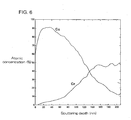
- the existence ratios of the first metal 35 and the second metal 36 to the thin metal layer 2 with respect to the thickness direction of the thin metal layer 2 can be determined by the analysis using the Auger electron spectroscopy (Auger analysis), for example.
- the first metal 35 and the second metal 36 are coexistent with each other so that the proportion of the first metal 35 to the second metal 36 (first metal/second metal) can become decreased gradually from the first unevenly-distributed metal portion 4 to the second unevenly-distributed metal portion 5.
- the thin metal layer 2 has thickness of e.g. 10-500nm, or preferably 50-300nm, and it is preferable that the metal coexisting portion 3 exists in the proportion of 50% or more, or preferably 80-100%, of the total dimension of the thin metal layer 2 with respect to the thickness direction thereof. When the proportion of the metal coexisting portion 3 is less than 50%, the thin metal layer 2 may peel easily after the passage of endurance time.
- the first unevenly-distributed metal portion 4 exists in the proportion of less than 50%, or preferably not more than 20%, of the total dimension of the thin metal layer 2 with respect to the thickness direction thereof
- the second unevenly-distributed metal portion 5 exists in the proportion of less than 50%, or preferably not more than 20%, of the total dimension of the thin metal layer 2 with respect to the thickness direction thereof.
- This thin metal layer 2 may be formed by a proper method without any particular limitation.
- this thin metal layer 2 is formed by using a vacuum evaporation method, or preferably by sputtering using sputtering equipment 21 shown in FIG. 3.
- the sputtering equipment 21 shown in FIG. 3 is a magnetron type continuous sputtering equipment comprising a vacuum chamber 22, and an electrode roll 23, a plasma electrode 26, a first sputtering electrode 24, a second sputtering electrode 25, an feed shaft 27, a wind-up shaft 28, two feed-side guide rolls 29, 30, and two wind-up side guide rolls 31, 32, all of which are provided in the vacuum chamber 22.
- the plasma electrode 26, the first sputtering electrode 24, and the second sputtering electrode 25 are disposed opposite to the electrode roll 23 at predetermined spaces and are arranged in order at circumferentially spaced locations from an upstream side of a rotation direction of the electrode roll 3 toward a downstream of the same.
- the feed shaft 27 and the wind-up shaft 28 are disposed on a side of the electrode roll 23 opposite the plasma electrode 26, the first sputtering electrode 24, and the second sputtering electrode 25.
- the two feed-side guide rolls 29, 30 are disposed between the feed shaft 27 and the electrode roll 23, and the two wind-up side guide rolls 31, 32 are disposed between the wind-up shaft 28 and the electrode roll 23.
- the insulating base layer 1 in the form of an elongate film is wound around the feed shaft 27.
- the insulating base layer 1 is fed out from the feed shaft 27 and guided to the electrode roll 23 along the feed-side guide rolls 29, 30. Sequentially, it is moved along an outer circumferential surface of the electrode roll 23 by the rotation of the electrode roll 23 and guided to the wind-up shaft 28 along the wind-up side guide rolls 31, 32 and wound by the wind-up shaft 28.
- the first sputtering electrode 24 and the second sputtering electrode 25 are connected with direct-current power sources 33, 34, respectively, and the first metal 35 and the second metal 36, which are used as sputtering targets, are placed on a discharge surface of the first sputtering electrode 24 and a discharge surface of the second sputtering electrode 25, respectively.
- the first sputtering electrode 24 and the second sputtering electrode 25 are disposed so adjacently that a first metal diffusing region 37 in which the first metal 35 placed on the discharge surface of the first sputtering electrode 24 is diffused on a surface of the insulating base layer 1 by sputtering and a second metal diffusing region 38 in which the second metal 36 placed on the discharge surface of the second sputtering electrode 25 is diffused on a surface of the insulating base layer 1 by sputtering are overlapped with each other.
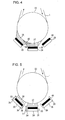
- target covers 39 to surround the sputtering electrode 24 and the second sputtering electrode 25 are arranged to prevent the first metal diffusing region 37 and the second metal diffusing region 38 being overlapped with each other, as shown in FIG. 5.
- the target covers 39 stand from the circumference of the first sputtering electrode 24 and that of the second sputtering electrode 25, respectively, to extend in a direction in which the first sputtering electrode 24 and the second sputtering electrode 25 are opposed to the electrode roll 23.
- the respective target covers 39 serve to prevent the first metal 35 diffusing region and the second metal 36 diffusing region being overlapped with each other.
- the sputtering equipment 21 of the present invention is constructed to allow the first metal diffusing region 37 and the second metal diffusing region 38 to be overlapped with each other without the target covers 39 (by removing the target covers 39 from the existing sputtering equipment 21.)
- the target covers 39 may be provided so that an existence ratio of the metal coexisting portion 3 to the thin metal layer 2 with respect to the thickness direction thereof can be controlled by adjusting heights T1, T2 of the target covers 39 (T1 is a height of the target cover 39 standing from the circumferential of the first sputtering electrode 24, and T2 is a height of the target cover 39 standing from the circumferential of the second sputtering electrode 25) (Cf. Example as will be described later).
- an ambient gas is filled in the vacuum chamber 22 to draw a vacuum, first.
- inert gases such as, for example, argon, neon, xenon, and krypton may be used as the ambient gas.
- argon is preferably used.
- the degree of vacuum is set to be e.g. 5 ⁇ 10 -3 - 1.6Pa, or preferably 5 ⁇ 10 -2 - 1.6 ⁇ 10 -1 Pa.
- the insulting base layer 1 wound around the feed shaft 27 is fed out by the feed shaft 27 and guided to the electrode roll 23 along the two feed-side guide rolls 29, 30. Thereafter, it is moved along the outer circumferential surface of the electrode roll 23 by the rotation of the electrode roll 23. Also, voltages are applied from the direct-current electrodes 33, 34 to the first sputtering electrode 24 and the second sputtering electrode 25, respectively, to sputter the first metal 35 and the second metal 36, respectively.
- the first metal 35 diffused due to the sputtering is deposited on the insulating base layer 1 within the first metal diffusing region 37 (except an overlapping region 40 mentioned below).
- the first unevenly-distributed metal portion 4 is formed on the insulating base layer 1 in the manner mentioned above.
- the second metal 36 may be diffused even in the first metal diffusing region 37 (except the overlapping region 40 mentioned below).
- the first metal 35 is deposited on the surface of the insulating base layer 1 so that the proportion of the first metal 35 to the second metal 36 becomes decrease gradually from the upstream side of the rotation direction of the electrode roll 23 to the downstream of the same.
- the second metal 36 is hardly diffused in the first metal diffusing region 37 (except the overlapping region 40 mentioned below)
- only the first metal 35 is substantially deposited on the insulating base layer 1 in the first metal diffusing region 37 (except the overlapping region 40 mentioned below).
- the insulating base layer 1 enters the overlapping region 40 where the first metal diffusing region 37 and the second metal diffusing region 38 are overlapped with each other, the first metal 35 and the second metal 36 diffused due to the sputtering are deposited on the insulating base layer 1. This can allow formation of the metal coexisting portion 3 on the first unevenly-distributed metal portion 4.
- first metal 35 and the second metal 36 are diffused in a mixed state in the overlapping region 40, and the first metal 35 and the second metal 36 are deposited on the surface of the insulating base layer 1 so that the proportion of the first metal 35 to the second metal 36 becomes decrease gradually from the upstream side of the rotation direction of the electrode roll 23 to the downstream of the same.
- the insulating base layer 1 enters the second metal diffusing region 38 (except the overlapping region 40).
- the second metal 36 diffused due to the sputtering is deposited on the insulating base layer 1. This can allow a formation of the second unevenly-distributed metal portion 5 on the metal coexisting portion 3.
- the second metal 36 is deposited on the surface of the insulating base layer 1 so that the proportion of the second metal 36 to the first metal 35 becomes increase gradually from the upstream side of the rotation direction of the electrode roll 23 to the downstream of the same.
- the first metal 35 is hardly diffused in the second metal diffusing region 38 (except the overlapping region 40)
- only the second metal 36 is substantially deposited on the insulating base layer 1 in the second metal diffusing region 38 (except the overlapping region 40).
- a high-frequency power source 43 is connected to the plasma electrode 26 through a matching circuit 42, and an ingot of metal 44 is placed on the discharge surface of the plasma electrode 26.
- the plasma electrode 26 is used when the surface of the insulating base layer 1 is subjected to plasma processing to reform the surface of the insulating base layer 1.
- high-frequency voltage is applied from the high-frequency power source 43 to the plasma electrode 26 through the matching circuit 42.
- the conductive pattern 6 is formed on the thin metal layer 2 of the wired circuit forming board 10 thus produced.
- the conductive pattern 6 is formed in the form of a wired circuit pattern by the additive process.
- a plating resist 7 of a pattern reverse to the wired circuit pattern is formed on the surface of the thin metal layer 2, as shown in FIG. 1(c).
- the plating resist 7 is formed in the form of a resist pattern reverse to the wired circuit pattern by laminating a dry film photoresist on the entire surface of the thin metal layer 2, then exposing the dry film photoresist to light, and developing it.
- the plating resist 7 usually has a thickness of 5-30 ⁇ m, or preferably 10-20 ⁇ m.
- the conductive pattern 6 is formed in the form of the wired circuit pattern on the surface of the thin metal layer 2 exposed from the plating resist 7, as shown in FIG. 1(d).
- the conductive materials that may be used for the conductive pattern 6 include, for example, copper, nickel, gold, solder, or alloys thereof. Copper is preferably used. Also, the conductive pattern 6 is formed by plating such as electroless plating and electrolytic plating. Preferably, the electrolytic plating is used. To be more specific, the conductive pattern 6, which is formed of copper, is formed by electrolytic copper plating in the form of the wired circuit pattern on an area of the thin metal layer 2 where the plating resist 7 is not formed. Plating solutions that may be used for the electrolytic copper plating include, for example, plating solution of copper sulfate, and plating solution of copper pyrophosphate.
- the conductive pattern 6 usually has thickness of 3-20 ⁇ m, or preferably 5-15 ⁇ m.
- a known etching process such as a chemical etching (wet etching) using alkaline solution such as solution of sodium hydroxide as the etching solution, or stripping is used for the removal of the plating resist 7.
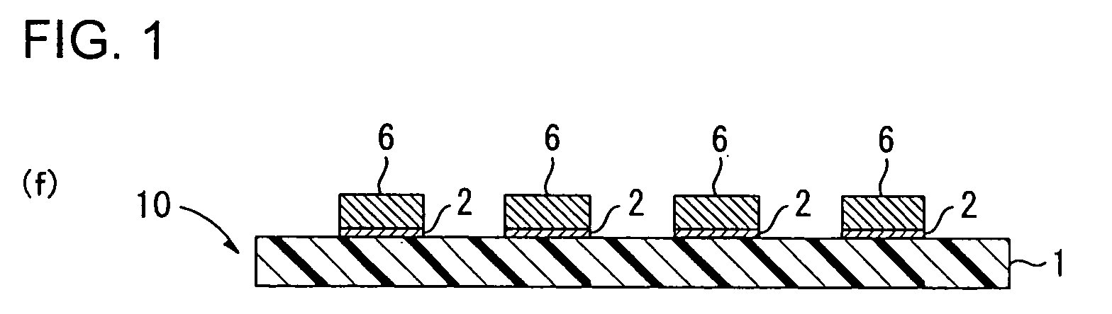
- the thin metal layer 2 exposed from the conductive pattern 6 is removed, as shown in FIG. 1(f).
- a known etching process such as a chemical etching (wet etching) using solution of ferric chloride, solution of potassium ferrocyanide, or the like as the etching solution, is used for the removal of the thin metal layer 2.
- a metal plating layer such as a nickel plating layer and a gold plating layer, may be formed on the surface of the conductive pattern 6 thus formed by a plating process, such as the electrolytic plating or the electroless plating.
- an insulating cover layer 8 may be formed on the insulating base layer 1, to cover the conductive pattern 6, if necessary, as shown in FIG. 1(g).
- the flexible wired circuit board is produced in the manner as mentioned above.
- the same synthetic resin used for the insulating base layer 1 may be used for the insulating cover layer 8.
- polyimide resin is used for the insulating cover layer.
- the insulating cover layer 8 can be formed, for example, by coating solution of photosensitive resin over the insulating base layer 1 including the conductive pattern 6, then exposing the coat to light and developing it to be formed in a predetermined pattern, and then curing it.
- the insulating cover layer 8 usually has a thickness of 2-50 ⁇ m, or preferably 5-30 ⁇ m.
- the thin metal layer 2 comprises three broadly classified portions, i.e., the first unevenly-distributed metal portion 4 adjacent to the insulating base layer 1, the second unevenly-distributed metal portion 5 adjacent to the conductive pattern 6, and the metal coexisting portion 3 interposed between the first unevenly-distributed metal portion 4 and the second unevenly-distributed metal portion 5, and these three portions are continuously present in the thin metal layer 2 without defining any boundaries therebetween.
- This construction can provide an improved adhesion between the insulating base layer 1 and the conductive pattern 6 by using nickel, chromium, or chromium alloy having a good adhesion with the insulating base layer 1 as the first metal 35 unevenly distributed in the first unevenly-distributed metal portion 4, and using copper having a good adhesion with the conductive pattern 6 as the second metal 36 unevenly distributed in the second unevenly-distributed metal portion 5.
- the first unevenly-distributed metal portion 4, the second unevenly-distributed metal portion 5 and the metal coexisting portion 3 are continuously present in the thin metal layer 2 without defining any boundaries therebetween, generation of delamination between the first metal 35 and the second metal 36 in the thin metal layer 2 can be prevented, and as such can prevent the delamination of the conductive pattern 6.
- the method for forming the thin metal layer 2 can allow formation of the thin metal layer 2 wherein the first unevenly-distributed metal portion 4, the second unevenly-distributed metal portion 5 and the metal coexisting portion 3 are continuously present in the thin metal layer 2 without defining any boundaries therebetween with ease and reliability by simply sputtering the first metal 35 and the second metal 36 in such a condition that the first metal diffusing region 37 and the second metal diffusing region 38 are overlapped with each other using the sputtering equipment 21.
- the insulating base layer of a polyimide resin film of 25 ⁇ m thick was wound around the feed shaft (Cf. FIG. 1(a)). Then, chromium forming the first metal was placed on a discharge side of the first sputtering electrode, and copper forming the second metal was placed on a discharge side of the second sputtering electrode. Thereafter, argon was filled in the vacuum chamber, so that the degree of vacuum in the vacuum chamber was set at 1 ⁇ 10 -1 Pa.
- the insulating base layer was fed out by the feed shaft and was moved along the outer circumferential surface of the electrode roll by the rotation of the electrode roll.
- voltages were applied to the first sputtering electrode and the second sputtering electrode from their respective direct-current power sources, whereby the chromium and the copper were sputtered on the insulating base layer moving along the outer circumferential surface of the electrode roll.
- the thin metal layer in which the first unevenly-distributed metal portion, the metal coexisting portion, and the second unevenly-distributed metal portion were present continuously without defining any boundaries therebetween was formed on the insulating base layer, to thereby produce the wired circuit forming board (Cf. FIG. 1(b)).
- the existence ratios among the first unevenly-distributed metal portion, the metal coexisting portion, and the second unevenly-distributed metal portion with respect to the thickness dimension of the thin metal layer are shown in TABLE 1.
- the dry film photoresist was laminated on the entire surface of the thin metal layer, it was exposed to light and developed, whereby the plating resist having thickness of 15 ⁇ m was formed in the form of the resist pattern reverse to the wired circuit pattern (Cf. FIG. 1(c)).
- the conductive pattern having thickness of 10 ⁇ m was formed in the wired circuit pattern on the surface of the thin metal layer exposed from the plating resist by electrolytic copper plating using plating solution of copper sulfate (Cf. FIG. 1(d)).
- the plating resist was removed by chemical etching using solution of sodium hydroxide (Cf. FIG. 1(e)).
- the thin metal layer exposed from the conductive pattern was removed by chemical etching using solution of ferric chloride (Cf. FIG. 1(f)).
- the flexible wired circuit board was produced in the manner mentioned above.
- a nickel plating layer and a gold plating layer were formed on the conductive pattern of each of the Examples by electrolytic nickel plating and electrolytic gold plating, respectively. Then, after those samples were allowed to stand for 168 hours, 240 hours, 360 hours, and 480 hours in an atmosphere of relative humidity of 60% and temperature of 90°C, cellophane tapes were adhered to a surface of the conductive pattern (gold plating layer) and then peeled off , to evaluate the presence of the delamination of the conductive pattern.
- the delamination time that elapses before delaminartion is shown in TABLE 1.
Landscapes
- Chemical & Material Sciences (AREA)
- Engineering & Computer Science (AREA)
- Organic Chemistry (AREA)
- Materials Engineering (AREA)
- Mechanical Engineering (AREA)
- Metallurgy (AREA)
- Chemical Kinetics & Catalysis (AREA)
- Manufacturing & Machinery (AREA)
- Microelectronics & Electronic Packaging (AREA)
- Inorganic Chemistry (AREA)
- Manufacturing Of Printed Wiring (AREA)
- Parts Printed On Printed Circuit Boards (AREA)
- Physical Vapour Deposition (AREA)
- Structure Of Printed Boards (AREA)
Abstract
Description
| Height of Target Cover (mm) | Thickness of Thin Metal Layer | Existence Ratio in Thickness Direction of Thin Metal Layer (%) | Delamination time (h) | ||||
| | T2 | 1st unevenly-distributed | 2nd unevenly-distributed metal portion | Metal coexisting portion | |||
| Ex. 1 | 0 | 0 | 200 | 0 | 0 | 100 | 480< |
| Ex. 2 | 15 | 0 | 200 | 0 | 10 | 90 | 480< |
| Ex. 3 | 15 | 15 | 200 | 10 | 10 | 80 | 480< |
| Ex. 4 | 20 | 20 | 200 | 15 | 20 | 65 | 480 |
| Ex. 5 | 30 | 30 | 200 | 20 | 30 | 50 | 480 |
| Ex. 6 | 35 | 35 | 200 | 20 | 50 | 30 | 360 |
| Ex. 7 | 45 | 45 | 200 | 25 | 65 | 10 | 240 |
| Ex.8 | 60 | 60 | 200 | 25 | 70 | 5 | 240 |
Claims (8)
- A wired circuit forming board comprising an insulating layer, and a thin metal layer formed on the insulating layer,
wherein the thin metal layer comprises at least two kinds of metals and is formed to prevent formation of an interface between the metals of different kinds in the thickness direction of the thin metal layer by the presence of a metal coexisting portion where the metals of different kinds are coexistent with each other. - The wired circuit forming board according to Claim 1, wherein the metal coexisting portion exists in a thickness direction of the thin metal layer in the proportion of 50% or more.
- The wired circuit forming board according to Claim 1, wherein the thin metal layer comprises a first metal and a second metal, and has a high existence ratio of the first metal to the second metal on one thicknesswise side thereof adjacent to the insulating layer and a high existence ratio of the second metal to the first metal on the other thicknesswise side thereof not adjacent to the insulating layer, and wherein the metal coexisting portion exists at least partway along the thickness direction of the thin metal layer.
- The wired circuit forming board according to Claim 3, wherein the second metal is copper.
- The wired circuit forming board according to Claim 3, wherein the first metal is chromium or alloy thereof.
- The wired circuit forming board according to Claim 3, wherein the thin metal layer is formed by sputtering the first metal and the second metal sequentially on a surface of the insulating layer, and the metal coexisting portion is formed by a first metal diffusing region for the first metal to be diffused on the surface of the insulating layer due to the sputtering and a second metal diffusing region for the second metal to be diffused on the surface of the insulating layer due to the sputtering being overlapped with each other.
- A wired circuit board comprises (i) a wired circuit forming board which comprises an insulating layer and a thin metal layer formed on the insulating layer and in which the thin metal layer comprises at least two kinds of metals and is formed to prevent a formation of an interface between the metals of different kinds in the thickness direction of the thin metal layer by the presence of a metal coexisting portion where the metals of different kinds are coexistent with each other, and (ii) a conductive pattern formed on the thin metal layer of the wired circuit forming board.
- A method for forming a thin metal layer by sputtering a first metal and a second metal on a surface of the insulating layer, wherein the first metal and the second metal are sputtered in such a condition that a first metal diffusing region for the first metal to be diffused on the surface of the insulating layer due to the sputtering and a second metal diffusing region for the second metal to be diffused on the surface of the insulating layer due to the sputtering are overlapped with each other.
Applications Claiming Priority (2)
| Application Number | Priority Date | Filing Date | Title |
|---|---|---|---|
| JP2004180245A JP3962039B2 (en) | 2004-06-17 | 2004-06-17 | Wiring circuit forming substrate, wiring circuit substrate, and method for forming metal thin layer |
| JP2004180245 | 2004-06-17 |
Publications (2)
| Publication Number | Publication Date |
|---|---|
| EP1608211A2 true EP1608211A2 (en) | 2005-12-21 |
| EP1608211A3 EP1608211A3 (en) | 2007-10-17 |
Family
ID=34936692
Family Applications (1)
| Application Number | Title | Priority Date | Filing Date |
|---|---|---|---|
| EP05010861A Withdrawn EP1608211A3 (en) | 2004-06-17 | 2005-05-19 | Wired circuit forming board, wired circuit board and thin metal layer forming method |
Country Status (6)
| Country | Link |
|---|---|
| US (1) | US7417316B2 (en) |
| EP (1) | EP1608211A3 (en) |
| JP (1) | JP3962039B2 (en) |
| KR (1) | KR101120526B1 (en) |
| CN (1) | CN1725933B (en) |
| TW (1) | TWI350721B (en) |
Cited By (1)
| Publication number | Priority date | Publication date | Assignee | Title |
|---|---|---|---|---|
| EP2406409B1 (en) * | 2009-03-12 | 2018-10-10 | Centre National de la Recherche Scientifique (CNRS) | Decoration by magnetron plasma sputtering onto glass containers for the cosmetic sectors |
Families Citing this family (11)
| Publication number | Priority date | Publication date | Assignee | Title |
|---|---|---|---|---|
| US7804172B2 (en) * | 2006-01-10 | 2010-09-28 | Halliburton Energy Services, Inc. | Electrical connections made with dissimilar metals |
| CN101489346B (en) * | 2008-01-15 | 2011-11-16 | 欣兴电子股份有限公司 | Patterned structure of circuit board |
| TWI398933B (en) * | 2008-03-05 | 2013-06-11 | 榮創能源科技股份有限公司 | Package structure of integrated circuit component and manufacturing method thereof |
| CN101840988A (en) * | 2010-04-22 | 2010-09-22 | 傲迪特半导体(南京)有限公司 | Automobile headlight radiation PCB drill base and manufacturing method thereof |
| EP3030061B1 (en) * | 2013-07-29 | 2021-01-06 | Kyocera Corporation | Wiring substrate, wiring substrate with lead, and electronic device |
| TWI488549B (en) * | 2014-03-07 | 2015-06-11 | Azotek Co Ltd | Metal substrate and fabricating method thereof |
| JP2015133167A (en) * | 2015-04-22 | 2015-07-23 | 大日本印刷株式会社 | Suspension board, suspension, suspension with element, and hard disk drive |
| US10180708B2 (en) | 2016-05-24 | 2019-01-15 | Microsoft Technology Licensing, Llc | Curved circuit board |
| KR20180058626A (en) * | 2016-11-24 | 2018-06-01 | 주식회사 아모그린텍 | Flat cable manufacturing method |
| CN108055790B (en) * | 2017-12-06 | 2019-10-18 | 深圳市和美源电子有限公司 | A kind of circuit board and preparation method thereof and application |
| KR102847046B1 (en) * | 2019-05-08 | 2025-08-18 | 삼성디스플레이 주식회사 | Display device and method of manufacturing for the display device |
Family Cites Families (14)
| Publication number | Priority date | Publication date | Assignee | Title |
|---|---|---|---|---|
| DE1097234B (en) * | 1958-06-26 | 1961-01-12 | Bosch Gmbh Robert | Process for coating objects with silver by vapor deposition in a vacuum using an adhesive chromium interlayer |
| LU46411A1 (en) * | 1964-06-27 | 1972-01-01 | ||
| US3881884A (en) * | 1973-10-12 | 1975-05-06 | Ibm | Method for the formation of corrosion resistant electronic interconnections |
| US4917963A (en) * | 1988-10-28 | 1990-04-17 | Andus Corporation | Graded composition primer layer |
| JPH0382188A (en) * | 1989-08-25 | 1991-04-08 | Kyocera Corp | Manufacture of ceramic wiring board |
| JPH04235272A (en) | 1991-01-11 | 1992-08-24 | Kobe Steel Ltd | Vapor-deposited al-mn series alloy plating material having good corrosion resistance and workability and its production |
| JP3422371B2 (en) | 1993-01-13 | 2003-06-30 | 石川島播磨重工業株式会社 | Continuous vacuum deposition method |
| US5874174A (en) * | 1995-08-09 | 1999-02-23 | Matsushita Electric Industrial Co., Ltd. | Conductor film and its forming method |
| JPH1192579A (en) | 1997-09-19 | 1999-04-06 | Nitto Denko Corp | Plasma treatment method for organic substrate and method for forming metal layer on organic substrate |
| JPH11158613A (en) | 1997-12-01 | 1999-06-15 | Canon Inc | Electrode substrate and method of manufacturing the electrode substrate |
| US6328858B1 (en) * | 1998-10-01 | 2001-12-11 | Nexx Systems Packaging, Llc | Multi-layer sputter deposition apparatus |
| JP4430165B2 (en) | 1999-09-02 | 2010-03-10 | 日東電工株式会社 | Vacuum thin film forming apparatus and vacuum thin film forming method |
| JP2003318533A (en) | 2002-04-24 | 2003-11-07 | Toyo Metallizing Co Ltd | Flexible printed wiring board |
| TW587322B (en) * | 2002-12-31 | 2004-05-11 | Phoenix Prec Technology Corp | Substrate with stacked via and fine circuit thereon, and method for fabricating the same |
-
2004
- 2004-06-17 JP JP2004180245A patent/JP3962039B2/en not_active Expired - Fee Related
-
2005
- 2005-05-19 EP EP05010861A patent/EP1608211A3/en not_active Withdrawn
- 2005-06-08 US US11/147,345 patent/US7417316B2/en not_active Expired - Fee Related
- 2005-06-10 TW TW094119239A patent/TWI350721B/en not_active IP Right Cessation
- 2005-06-16 KR KR1020050051930A patent/KR101120526B1/en not_active Expired - Fee Related
- 2005-06-17 CN CN2005100811017A patent/CN1725933B/en not_active Expired - Fee Related
Cited By (1)
| Publication number | Priority date | Publication date | Assignee | Title |
|---|---|---|---|---|
| EP2406409B1 (en) * | 2009-03-12 | 2018-10-10 | Centre National de la Recherche Scientifique (CNRS) | Decoration by magnetron plasma sputtering onto glass containers for the cosmetic sectors |
Also Published As
| Publication number | Publication date |
|---|---|
| US7417316B2 (en) | 2008-08-26 |
| TW200601921A (en) | 2006-01-01 |
| CN1725933A (en) | 2006-01-25 |
| JP3962039B2 (en) | 2007-08-22 |
| CN1725933B (en) | 2010-10-06 |
| EP1608211A3 (en) | 2007-10-17 |
| KR20060049235A (en) | 2006-05-18 |
| KR101120526B1 (en) | 2012-02-24 |
| TWI350721B (en) | 2011-10-11 |
| JP2006005176A (en) | 2006-01-05 |
| US20050280153A1 (en) | 2005-12-22 |
Similar Documents
| Publication | Publication Date | Title |
|---|---|---|
| KR101048967B1 (en) | Manufacturing method of flexible wiring circuit board | |
| US8522427B2 (en) | Method of manufacturing a printed circuit board | |
| US7417316B2 (en) | Wired circuit forming board, wired circuit board, and thin metal layer forming method | |
| US11653454B2 (en) | Printed wiring board and manufacturing method thereof | |
| EP1167580B1 (en) | Electrolytic copper foil | |
| WO2001016402A1 (en) | Electrolytic copper foil with carrier foil and method for manufacturing the same and copper-clad laminate using the electrolytic copper foil with carrier foil | |
| JPH09136378A (en) | Copper thin film substrate and printed wiring board | |
| WO1995003168A1 (en) | Circuit board material with barrier layer | |
| CN118019210A (en) | Metal foil, circuit boards, copper-clad laminates, negative electrode materials for batteries, and batteries | |
| US4812213A (en) | Process for the manufacture of multi-layer circuits with dynamic flexing regions and the flexible circuits made therefrom | |
| WO2004021749A3 (en) | Manufacture of flexible printed circuit boards | |
| US7507434B2 (en) | Method and apparatus for laminating a flexible printed circuit board | |
| US20080000679A1 (en) | Wired circuit board and producing method thereof | |
| JPH11317574A (en) | Composite copper foil, method for producing the same, and copper-clad laminate and printed wiring board using the composite copper foil | |
| JP3888587B2 (en) | Etching method of flexible substrate | |
| KR20030044046A (en) | Use of metallic treatment on copper foil to produce fine lines and replace oxide process in printed circuit board production | |
| JP2004014975A (en) | Flexible circuit board with metal foil | |
| JP7711413B2 (en) | Manufacturing method of copper clad laminate | |
| JP2007245646A (en) | Two-layered film, its manufacturing method and manufacturing method of printed circuit board | |
| JP7767822B2 (en) | Copper-clad laminate and method for manufacturing the same | |
| JP7787493B2 (en) | Copper-clad laminate and method for manufacturing the same | |
| JP2542428B2 (en) | Method for manufacturing double-sided flexible printed circuit board | |
| KR20220133495A (en) | Environmentally Friendly Flexible Circuit Board Using Non-Adhesive Coarse Laminated Plates and Its Manufacturing Method | |
| JP2023005364A (en) | Copper-clad laminate and method for producing copper-clad laminate | |
| JP2023177986A (en) | Manufacturing method for metal clad laminates |
Legal Events
| Date | Code | Title | Description |
|---|---|---|---|
| PUAI | Public reference made under article 153(3) epc to a published international application that has entered the european phase |
Free format text: ORIGINAL CODE: 0009012 |
|
| AK | Designated contracting states |
Kind code of ref document: A2 Designated state(s): AT BE BG CH CY CZ DE DK EE ES FI FR GB GR HU IE IS IT LI LT LU MC NL PL PT RO SE SI SK TR |
|
| AX | Request for extension of the european patent |
Extension state: AL BA HR LV MK YU |
|
| PUAL | Search report despatched |
Free format text: ORIGINAL CODE: 0009013 |
|
| AK | Designated contracting states |
Kind code of ref document: A3 Designated state(s): AT BE BG CH CY CZ DE DK EE ES FI FR GB GR HU IE IS IT LI LT LU MC NL PL PT RO SE SI SK TR |
|
| AX | Request for extension of the european patent |
Extension state: AL BA HR LV MK YU |
|
| 17P | Request for examination filed |
Effective date: 20071113 |
|
| AKX | Designation fees paid |
Designated state(s): DE FR GB |
|
| 17Q | First examination report despatched |
Effective date: 20120906 |
|
| STAA | Information on the status of an ep patent application or granted ep patent |
Free format text: STATUS: THE APPLICATION IS DEEMED TO BE WITHDRAWN |
|
| 18D | Application deemed to be withdrawn |
Effective date: 20130117 |