EP1608019B1 - Imaging sensor - Google Patents
Imaging sensor Download PDFInfo
- Publication number
- EP1608019B1 EP1608019B1 EP04253557A EP04253557A EP1608019B1 EP 1608019 B1 EP1608019 B1 EP 1608019B1 EP 04253557 A EP04253557 A EP 04253557A EP 04253557 A EP04253557 A EP 04253557A EP 1608019 B1 EP1608019 B1 EP 1608019B1
- Authority
- EP
- European Patent Office
- Prior art keywords
- well
- epitaxial material
- separating region
- imaging sensor
- photo
- Prior art date
- Legal status (The legal status is an assumption and is not a legal conclusion. Google has not performed a legal analysis and makes no representation as to the accuracy of the status listed.)
- Expired - Lifetime
Links
- 238000003384 imaging method Methods 0.000 title claims description 70
- 239000007943 implant Substances 0.000 claims description 120
- 239000000463 material Substances 0.000 claims description 106
- 238000012545 processing Methods 0.000 claims description 23
- 239000002184 metal Substances 0.000 claims description 10
- 239000004020 conductor Substances 0.000 claims description 9
- 230000003287 optical effect Effects 0.000 claims description 6
- 238000006243 chemical reaction Methods 0.000 description 14
- 238000000034 method Methods 0.000 description 7
- 239000003990 capacitor Substances 0.000 description 6
- 230000010354 integration Effects 0.000 description 6
- 238000004519 manufacturing process Methods 0.000 description 5
- 238000010586 diagram Methods 0.000 description 4
- 230000035945 sensitivity Effects 0.000 description 4
- 230000007423 decrease Effects 0.000 description 3
- 230000003247 decreasing effect Effects 0.000 description 3
- 238000013461 design Methods 0.000 description 3
- 238000009792 diffusion process Methods 0.000 description 3
- 230000006870 function Effects 0.000 description 3
- 238000009738 saturating Methods 0.000 description 3
- 239000000758 substrate Substances 0.000 description 3
- 241000699666 Mus <mouse, genus> Species 0.000 description 2
- 230000000694 effects Effects 0.000 description 2
- 230000003071 parasitic effect Effects 0.000 description 2
- 230000008569 process Effects 0.000 description 2
- 230000009467 reduction Effects 0.000 description 2
- 238000000926 separation method Methods 0.000 description 2
- 241000699670 Mus sp. Species 0.000 description 1
- 206010034960 Photophobia Diseases 0.000 description 1
- 238000013459 approach Methods 0.000 description 1
- 230000000295 complement effect Effects 0.000 description 1
- 238000005516 engineering process Methods 0.000 description 1
- 238000002513 implantation Methods 0.000 description 1
- 238000002955 isolation Methods 0.000 description 1
- 208000013469 light sensitivity Diseases 0.000 description 1
- 238000005259 measurement Methods 0.000 description 1
- 229910044991 metal oxide Inorganic materials 0.000 description 1
- 150000004706 metal oxides Chemical class 0.000 description 1
- 238000012986 modification Methods 0.000 description 1
- 230000004048 modification Effects 0.000 description 1
- 230000000541 pulsatile effect Effects 0.000 description 1
- 230000004044 response Effects 0.000 description 1
- 238000012552 review Methods 0.000 description 1
- 239000004065 semiconductor Substances 0.000 description 1
- 238000010561 standard procedure Methods 0.000 description 1
- 238000012546 transfer Methods 0.000 description 1
Images




Classifications
-
- H—ELECTRICITY
- H10—SEMICONDUCTOR DEVICES; ELECTRIC SOLID-STATE DEVICES NOT OTHERWISE PROVIDED FOR
- H10F—INORGANIC SEMICONDUCTOR DEVICES SENSITIVE TO INFRARED RADIATION, LIGHT, ELECTROMAGNETIC RADIATION OF SHORTER WAVELENGTH OR CORPUSCULAR RADIATION
- H10F39/00—Integrated devices, or assemblies of multiple devices, comprising at least one element covered by group H10F30/00, e.g. radiation detectors comprising photodiode arrays
- H10F39/80—Constructional details of image sensors
Definitions
- the present invention relates to an imaging sensor in particular an imaging sensor for use in a light to frequency converter.
- the present invention relates to imaging sensors and light to frequency converters, it is useful at this point to briefly review the dynamic range and noise characteristics of CMOS image sensors and the operation of the light to frequency converter circuit.
- CCDs charge coupled devices
- CMOS complementary metal oxide semiconductor
- CMOS imaging sensors can be produced using standard fabrication procedures which are already widely used for producing CMOS chips for computer processors, memory chips etc.
- CCDs require optimised charge transfer efficiency and thus specialised fabrication facilities. Consequently, CMOS imaging sensor fabrication is considerably less expensive than CCD fabrication.
- the signal processing and control circuitry for a CMOS imaging sensor can be integrated directly onto the CMOS chip.
- the functionality and size economy provided by the extra circuitry on CMOS imaging sensor chips comes at the cost of increased dark current.
- the maximal non-saturating input current (i max ) of an imaging sensor is a function of the sensor's well capacity (Q sat ), dark current (i dc ) and integration time t int.
- i max q ⁇ Q sat t int - i dc
- smallest photo-current (i min ) detectable by an imaging sensor is a function of the sensor's dark current, read noise ⁇ r 2 and integration time.
- i min q t int ⁇ 1 q ⁇ i dc ⁇ t int + ⁇ r 2
- the largest non-saturating input signal (i max ) of an imaging sensor can be increased by increasing the speed of the system (i.e. decreasing the integration time).
- decreasing the integration time of the imaging sensor also has the effect of increasing i min .
- the approach of decreasing the integration time of an imaging sensor will produce a limited increase in an imaging sensor's dynamic range.
- Another method of increasing an imaging sensor's dynamic range is to use larger photodiodes (i.e. with larger well capacity). However, this has the effect of increasing the imaging sensor's dark current i dc and thus increasing i min .
- Dark current is the leakage current generated at the integration node of a photo-detector in the absence of any optical signal. Dark current originates from thermally generated electron-hole pairs that produce junction and transistor leakages. Accordingly, dark current is a function of temperature and junction area.
- a light to frequency (LTF) converter as described in US Patent 5850195 , is a CMOS imaging sensor with a large dynamic range.
- the operation of the LTF converter will be described below with reference to the accompanying figures in which:
- the LTF converter comprises a control circuit 4, at least one photodiode(s) 6 and a current to digital signal converter 8.
- the control circuit 4 controls the sensitivity of the LTF converter in accordance with a number of user controllable input signals So, S 1 , S 2 and S 3 .
- the current to digital signal converter 8 uses a switched-capacitor charge metering technique to convert the photo-current generated by the photodiode(s) 6 to a digital signal of a specific frequency. In order to perform this conversion process, the current to digital signal converter 8 employs a bias circuit 10, a diode multiplexer circuit 12, an amplifier circuit 14, a switched capacitor network 16, a comparator 18 and a monostable multivibrator circuit 19.
- the bias circuit 10 receives a control signal from the control circuit 4 to control the sensitivity of the current to digital signal converter 8.
- the bias circuit 10 transmits a further control signal to the diode multiplexer circuit 12, which also receives the photo-current generated by the photodiode(s) 6.
- the switched-capacitor charge metering technique employed by the current to digital signal converter 8 is implemented by the amplifier circuit 14, capacitor network 16 and monostable multivibrator circuit 19.
- the diode multiplexer circuit 12 receives a photo-current from the photodiode(s) 6 and employs a charge sensing amplifier circuit 20 to effectively isolate the remaining circuitry of the current to digital signal converter 8 from the large capacitance of the photodiode(s) 6 ( ⁇ 100 pF).
- the charge sensing amplifier 20 comprises an operational amplifier 22 configured in a closed loop configuration with its non-inverting input coupled to ground and a feedback capacitor 24 connected to the inverting input. Since the operational amplifier 22 has a high input impedance, virtually no current flows through it. Consequently, since the non-inverting input of the operational amplifier 22 is connected to ground, the inverting input becomes a virtual ground.
- the output of the operational amplifier 24 changes to ensure that the inverting input of the operational amplifier 24 remains at the same potential as the non-inverting input.
- a current flows through the feedback capacitor 22 which has the same magnitude (but opposite sign) to the photo-current generated by the photodiode(s) 6 (i pd ).
- Equation 4 shows the relationship between the output voltage from the charge sensing amplifier 20 and the photo-current generated by the photodiode(s) 6.
- V out - i pd ⁇ T int C fb
- the diode multiplexer circuit 12 transmits a current signal corresponding with the photo-current generated by the photodiode(s) 6 (and processed by the charge sensing amplifier) to the amplifier circuit 14.
- the amplifier circuit 14 comprises at least one operational amplifier that integrates the voltage (V out ) generated from the photocurrent (i pd ). Since the closed loop gain bandwidth product of an operational amplifier is inversely related to the capacitive loading at its inputs, the significant reduction in capacitive loading provided by the diode multiplexer circuit 12 (and its charge sensing amplifier) permits the use of a lower frequency operational amplifier in the amplifier circuit 14.
- the reduction in capacitive loading made possible by the charge sensing amplifier in the diode multiplexer circuit 12 permits the use of larger photodiodes in the event of there being more than one photodiode 6 available.
- the increased output of the integrating amplifier (22) will reach a maximum value and be periodically reset.
- FIG. 4 shows a system used for resetting the integrating amplifier in the amplifier circuit 14.
- the output voltage from the amplifier circuit 14 (V out2 ) is transmitted to the comparator 18 of the current to digital signal converter 8.
- the comparator 18 the output voltage (V out2 ) is compared against a reference voltage (V ref ). If the output voltage (V out2 ) exceeds the reference voltage (V ref ), the comparator 18 transmits a control signal (Ctrl) to the monostable multivibrator circuit 19.
- the monostable multivibrator circuit 19 emits a pulsatile signal, with each pulse being used to generate a charge to discharge the integrating amplifier 22.
- the charge transferred to the integrating amplifier 22 with the emission of each pulse by the monostable multivibrator circuit 19 results in an average current that is equivalent to the photodiode current I pd . Consequently, the frequency of the control signal Ctrl is also proportional to the photodiode current I pd (assuming that the integrating amplifier in the amplifier circuit 14 settles completely during the period of the control signal).
- the control signal Ctrl is also fed to divide-by-two circuit 30 to form the output signal from the LTF converter. Once the output voltage from the integrating amplifier (V out2 ) is reduced to below the reference voltage (V ref ), the monostable multivibrator circuit 19 is disabled.
- the dynamic range of this system is F out max -F out min .
- the maximum frequency (F out max ) is typically determined by the maximum operating speed of the integrating amplifier in the amplifier circuit 14, which sets the maximum slew rate ("m" in Figure 5 ).
- the maximum frequency (F out max ) can be relatively easily influenced by the design of the on-board operational amplifiers (e.g. by reducing the parasitic capacitance of the operational amplifiers or increasing the bias currents of the operational amplifiers).
- the minimum frequency (F out min ) is typically determined by the dark current flowing through the photodiode(s) 6.
- FIGs 6 and 7 show top plan views of conventional LTF converter circuits comprising an LTF conversion circuit section 32 and a photo-generated electron collection section 33.
- the LTF conversion circuitry 32 e.g. control circuit and current to digital signal converter
- the LTF conversion circuitry 32 is comprised of N-MOS 34 and P-MOS 36 transistors embedded in a P-well 38 and N-well 40 material respectively.
- the photo-generated electron collection section 33 comprises a large N-Well photodiode 42 surrounding an N+ contact 43.
- the photo-generated electron collection section 33 comprises a large N+ photodiode 44.
- the photodiodes 42 or 44 must be isolated from the LTF conversion circuitry 32 by a P-Well material 46.
- the photo-current collected from the photodiode 42 or 44 is transmitted to the LTF conversion circuitry section 32 by a metal contact 48.
- Document JP 092 60 715 shows a P-type isolation region between the photodiode and the circuit in order to decrease parasitic capacity.
- an imaging sensor integrated circuit comprising a photo-current generating and collecting section and a signal processing section, formed on a P-epitaxial material and separated from each other by a separating region; wherein the photo-current generating and collecting section comprises an N-well implant into the P-epitaxial material; and the N-well implant comprises an N+ contact; characterised in that the separating region is implanted into the P-epitaxial material at substantially the same depth as the N-well implant; and the N-well implant is separated from the separating region by the P-epitaxial material, to form a photodiode PN junction between the N-well implant and the P-epitaxial material.
- the separating region is an N-well.
- the separating region is a P-well.
- the N-well implant is of 5-10 ⁇ m in length.
- an imaging sensor integrated circuit comprising a photo-current generating and collecting section and a signal processing section, formed on an N-epitaxial material and separated from each other by a separating region; wherein the photo-current generating and collecting section comprises a P-well implant into the N-epitaxial material and the P-well implant comprises a P+ contact; characterised in that the separating region is implanted into the N-epitaxial material at substantially the same depth as the P-well implant; and the P-well implant is separated from the separating region by the N-epitaxial material to form a photodiode PN junction between the P-well implant and the N-epitaxial material.
- the P-well implant is of 5-10 ⁇ m in length.
- an imaging sensor integrated circuit comprising a photo-current generating and collecting section and a signal processing section formed on a P-epitaxial material and separated from each other by a separating region; wherein the photo-current generating and collecting section comprises a plurality of N-well implants into the P-epitaxial material, each of the N-well implants comprising an N+ contact: characterised in that the separating region is implanted into the P-epitaxial material at substantially the same depth as the N-well implants and the N-well implants are separated from the separating region by the P-epitaxial material to form a plurality of photodiode PN junctions between the N-well implants and the P-epitaxial material.
- the separating region is an N-well.
- the separating region is a P-well.
- each of the plurality of N-well implants is of 5-10 ⁇ m in length.
- the plurality of N-well implants are separated from each other by distances of less than 50 ⁇ m.
- the plurality of N-well implants (84) are connected together by a metal conductor.
- the metal conductor sums the photo-current received from the plurality of connected N-well implants.
- an imaging sensor integrated circuit comprising a photo-current generating and collection section and a signal processing section formed on an N-epitaxial material and separated from each other by a separating region; wherein the photo-current generating and collecting section comprises a plurality of P-well implants into the N-epitaxial material, each of the P-well implants comprising a P+ contact; characterised in that:
- each of the plurality of P-well implants is of 5-10 ⁇ m in length.
- the plurality of P-well implants are separated from each other by distances of less than 50 ⁇ m.
- the plurality of P-well implants are connected together by a metal conductor.
- the metal conductor sums the photo-current received from the plurality of connected P-well implants.
- the signal processing section comprises a charge sensing amplifier.
- a light to frequency converter comprising an imaging sensor integrated circuit comprising a photo-current generating and collecting section and a signal processing section, formed on a P-epitaxial material and separated from each other by a separating region; wherein the photo-current generating and collecting section comprises an N-well implant into the P-epitaxial material; and the N-well implant comprises an N+ contact characterised in that:
- an optical mouse comprising an imaging sensor integrated circuit comprising a photo-current generating and collecting section and a signal processing section, formed on a P-epitaxial material and separated from each other by a separating region; wherein the photo-current generating and collecting section comprises an N-well implant into the P-epitaxial material; and the N-well implant comprises an N+ contact characterised in that:
- a digital camera comprising an imaging sensor integrated circuit comprising a photo-current generating and collecting section and a signal processing section, formed on a P-epitaxial material and separated from each other by a separating region; wherein the photo-current generating and collecting section comprises an N-well implant into the P-epitaxial material; and the N-well implant comprises an N+ contact characterised in that:
- a mobile phone comprising the digital camera of the seventh aspect.
- a light to frequency converter comprising an imaging sensor integrated circuit comprising a photo-current generating and collecting section and a signal processing section, formed on a P-epitaxial material and separated from each other by a separating region; wherein the photo-current generating and collecting section comprises an N-well implant into the P-epitaxial material; and the N-well implant comprises an N+ contact characterised in that:
- an optical mouse comprising an imaging sensor integrated circuit comprising a photo-current generating and collecting section and a signal processing section, formed on a P-epitaxial material and separated from each other by a separating region; wherein the photo-current generating and collecting section comprises an N-well implant into the P-epitaxial material; and the N-well implant comprises an N+ contact characterised in that:
- a digital camera comprising an imaging sensor integrated circuit comprising a photo-current generating and collecting section and a signal processing section, formed on a P-epitaxial material and separated from each other by a separating region; wherein the photo-current generating and collecting section comprises an N-well implant into the P-epitaxial material; and the N-well implant comprises an N+ contact characterised in that:
- a mobile phone comprising the digital camera of the eleventh aspect.
- the present invention reduces the dark current in an imaging sensor by reducing the interfacial area between its N-well and P-well components.
- the imaging sensor Since the imaging sensor is designed for use in an LTF converter, for the sake of clarity, the imaging sensor will be referred to henceforth as an improved dynamic range LTF converter. Similarly, since the imaging sensor employed in the second embodiment employs multiple photodiodes in an LTF converter, the second embodiment will henceforth be known as a multiple photodiode improved dynamic range LTF converter.
- the improved dynamic range LTF converter 50 comprises an LTF conversion circuitry section 132 and a photo-generated electron collection section 133.
- the LTF conversion circuitry section 132 comprises N-MOS 134 and P-MOS 136 transistors embedded in a P-well 138 and N-well 140 material respectively.
- the improved dynamic range LTF converter 50 uses a small N-Well photodiode 52 (typically 5-10 ⁇ m across) with a smaller N+ contact region 54 in its centre.
- the photodiode 52 must be isolated from the LTF conversion circuitry 132 by a P-Well 146 or an N-well 56.
- the implantation of the P-Well 146 is suppressed, leaving the high resistivity P-epitaxial material 58.
- photo-generated charge 60 will diffuse around the pixel and will probably be collected by the N-Well diode 52 especially since the operation of the LTF circuit renders the N-Well diode 52 the most positive node.
- the P-well 146 is connected to ground between the N-well 140 (biased positive at VDD) and the photo-generated electron collection section 133.
- the diffusion length of electrons in the P-epitaxial substrates used in modern CMOS technology is typically 30 ⁇ m-50 ⁇ m. At distances greater than this, electrons are likely to recombine and be lost within the substrate.
- the improved LTF converter shown in Figure 10 does not have this problem as the photodiode 52 is smaller than 50 ⁇ m.
- one method of increasing the sensitivity of an imaging sensor is to increase the size of its photodiodes.
- the limited diffusion length of electrons in the P-epitaxial substrate prevents a significant proportion of photo-generated electrons from reaching a collection node.
- Figure 12 shows a multiple photodiode improved dynamic range LTF converter that effectively permits the use of larger, more sensitive pixels.
- the multiple photodiode improved dynamic range LTF converter 80 comprises an LTF conversion circuitry section 232 and a photo-generated electron collection section 233.
- the LTF conversion circuitry section 232 comprises N-MOS 234 and P-MOS 236 transistors embedded in a P-well 238 and N-well 240 material respectively.
- the photo-generated electron collection section 233 comprises several regularly spaced (e.g. ⁇ 50 ⁇ m) collection nodes 82.
- each of the collection nodes 82 uses a small photodiode 84 from N-Well material (typically 5-10 ⁇ m across) with a smaller N+ contact region 86 in its centre.
- the 5 ⁇ m-10 ⁇ m collection nodes are connected together using a metal conductor 248 that sums the photo-current.
- the photodiodes 82 must be isolated from the LTF conversion circuitry section 232 by a P-Well 246.
- the improved dynamic range LTF converter can be readily included in an integrated circuit and is applicable to a broad range of devices including digital cameras, mobile phones incorporating a digital camera, and optical mice. It will be appreciated that the man skilled in the art may employ standard techniques in order to implement the invention in these and other ways.
Landscapes
- Solid State Image Pick-Up Elements (AREA)
- Transforming Light Signals Into Electric Signals (AREA)
Description
- The present invention relates to an imaging sensor in particular an imaging sensor for use in a light to frequency converter.
- Since the present invention relates to imaging sensors and light to frequency converters, it is useful at this point to briefly review the dynamic range and noise characteristics of CMOS image sensors and the operation of the light to frequency converter circuit.
- Until relatively recently, charge coupled devices (CCDs) maintained a dominant position in the field of digital imaging sensors. However, recent advances in the design and fabrication of complementary metal oxide semiconductor (CMOS) chips, have meant that CMOS imaging sensors are beginning to adopt a more dominant position in the low-cost imaging market.
- One of the main advantages of CMOS imaging sensors is that they can be produced using standard fabrication procedures which are already widely used for producing CMOS chips for computer processors, memory chips etc. In contrast, CCDs require optimised charge transfer efficiency and thus specialised fabrication facilities. Consequently, CMOS imaging sensor fabrication is considerably less expensive than CCD fabrication. Furthermore, in contrast with CCDs, the signal processing and control circuitry for a CMOS imaging sensor can be integrated directly onto the CMOS chip. However, the functionality and size economy provided by the extra circuitry on CMOS imaging sensor chips comes at the cost of increased dark current.
- Dynamic range is a measurement of an imaging sensor's ability to capture detail across a range of lighting conditions (i.e. from dark shadows to bright lighting). More specifically, referring to
equation 1 below, an imaging sensor's dynamic range (DR) may be defined as the ratio of the sensor's largest non-saturating current (imax) to the smallest photo-current (imin) detectable by the sensor.
- Consequently, from
equation 1 it can be seen that in order to increase the dynamic range of an imaging sensor it is necessary to increase imax and decrease imin. However, referring to equation 2 below, the maximal non-saturating input current (imax) of an imaging sensor is a function of the sensor's well capacity (Qsat), dark current (idc) and integration time tint.
- Similarly, referring to equation 3 below, smallest photo-current (imin) detectable by an imaging sensor is a function of the sensor's dark current, read noise


- From equation 2 above, it can be seen that the largest non-saturating input signal (imax) of an imaging sensor can be increased by increasing the speed of the system (i.e. decreasing the integration time). However, referring to equation 3 above, decreasing the integration time of the imaging sensor also has the effect of increasing imin. Thus, the approach of decreasing the integration time of an imaging sensor will produce a limited increase in an imaging sensor's dynamic range.
- Another method of increasing an imaging sensor's dynamic range is to use larger photodiodes (i.e. with larger well capacity). However, this has the effect of increasing the imaging sensor's dark current idc and thus increasing imin.
- Dark current is the leakage current generated at the integration node of a photo-detector in the absence of any optical signal. Dark current originates from thermally generated electron-hole pairs that produce junction and transistor leakages. Accordingly, dark current is a function of temperature and junction area.
- A light to frequency (LTF) converter, as described in
US Patent 5850195 , is a CMOS imaging sensor with a large dynamic range. The operation of the LTF converter will be described below with reference to the accompanying figures in which: -
Figure 1 is a block diagram of a LTF converter; -
Figure 2 is a circuit diagram of a charge sensing amplifier used in an amplifier circuit in the LTF converter; -
Figure 3 is a graph of the output voltage measured from the LTF converter's amplifier circuit over a period of time during which the LTF converter is exposed to light; -
Figure 4 is a circuit/block diagram of a number of the components of a current to digital signal converter block used in the LTF converter; -
Figure 5 is a timing diagram for the reference voltage (Vref), output voltage from the integrating amplifier (Vout2), the control signal from the comparator 18 (Ctrl) and the overall output signal from the LTF converter (Fout); -
Figure 6 is a top plan view of an N-well photodiode LTF converter; -
Figure 7 is a top plan view of an N+ photodiode LTF converter; and -
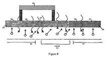
Figure 8 is a cross-sectional view of an N-well photodiode LTF converter or an N-well photodiode LTF converter as shown inFigure 6 andFigure 7 . - The LTF converter comprises a
control circuit 4, at least one photodiode(s) 6 and a current todigital signal converter 8. Thecontrol circuit 4 controls the sensitivity of the LTF converter in accordance with a number of user controllable input signals So, S1, S2 and S3. The current todigital signal converter 8 uses a switched-capacitor charge metering technique to convert the photo-current generated by the photodiode(s) 6 to a digital signal of a specific frequency. In order to perform this conversion process, the current todigital signal converter 8 employs abias circuit 10, adiode multiplexer circuit 12, anamplifier circuit 14, a switchedcapacitor network 16, acomparator 18 and amonostable multivibrator circuit 19. - The
bias circuit 10 receives a control signal from thecontrol circuit 4 to control the sensitivity of the current todigital signal converter 8. Thebias circuit 10 transmits a further control signal to thediode multiplexer circuit 12, which also receives the photo-current generated by the photodiode(s) 6. The switched-capacitor charge metering technique employed by the current todigital signal converter 8 is implemented by theamplifier circuit 14,capacitor network 16 andmonostable multivibrator circuit 19. - Referring to
Figure 2 , thediode multiplexer circuit 12 receives a photo-current from the photodiode(s) 6 and employs a chargesensing amplifier circuit 20 to effectively isolate the remaining circuitry of the current todigital signal converter 8 from the large capacitance of the photodiode(s) 6 (< 100 pF). Thecharge sensing amplifier 20 comprises anoperational amplifier 22 configured in a closed loop configuration with its non-inverting input coupled to ground and afeedback capacitor 24 connected to the inverting input. Since theoperational amplifier 22 has a high input impedance, virtually no current flows through it. Consequently, since the non-inverting input of theoperational amplifier 22 is connected to ground, the inverting input becomes a virtual ground. The output of theoperational amplifier 24 changes to ensure that the inverting input of theoperational amplifier 24 remains at the same potential as the non-inverting input. In the process, a current flows through thefeedback capacitor 22 which has the same magnitude (but opposite sign) to the photo-current generated by the photodiode(s) 6 (ipd). -
Equation 4 below shows the relationship between the output voltage from thecharge sensing amplifier 20 and the photo-current generated by the photodiode(s) 6.
- From the above expression it can be seen that the output voltage (Vout) from the
charge sensing amplifier 20 is independent of the photodiode(s)' 6 capacitance. - Returning to
Figure 1 , thediode multiplexer circuit 12 transmits a current signal corresponding with the photo-current generated by the photodiode(s) 6 (and processed by the charge sensing amplifier) to theamplifier circuit 14. Theamplifier circuit 14 comprises at least one operational amplifier that integrates the voltage (Vout) generated from the photocurrent (ipd). Since the closed loop gain bandwidth product of an operational amplifier is inversely related to the capacitive loading at its inputs, the significant reduction in capacitive loading provided by the diode multiplexer circuit 12 (and its charge sensing amplifier) permits the use of a lower frequency operational amplifier in theamplifier circuit 14. - Furthermore, the reduction in capacitive loading made possible by the charge sensing amplifier in the
diode multiplexer circuit 12 permits the use of larger photodiodes in the event of there being more than onephotodiode 6 available. However, referring toFigure 3 , the increased output of the integrating amplifier (22) will reach a maximum value and be periodically reset. -
Figure 4 shows a system used for resetting the integrating amplifier in theamplifier circuit 14. In this system, the output voltage from the amplifier circuit 14 (Vout2) is transmitted to thecomparator 18 of the current todigital signal converter 8. In thecomparator 18, the output voltage (Vout2) is compared against a reference voltage (Vref). If the output voltage (Vout2) exceeds the reference voltage (Vref), thecomparator 18 transmits a control signal (Ctrl) to themonostable multivibrator circuit 19. In response to the received control signal (Ctrl), themonostable multivibrator circuit 19 emits a pulsatile signal, with each pulse being used to generate a charge to discharge the integratingamplifier 22. - The charge transferred to the integrating
amplifier 22 with the emission of each pulse by themonostable multivibrator circuit 19 results in an average current that is equivalent to the photodiode current Ipd. Consequently, the frequency of the control signal Ctrl is also proportional to the photodiode current Ipd (assuming that the integrating amplifier in theamplifier circuit 14 settles completely during the period of the control signal). The control signal Ctrl is also fed to divide-by-twocircuit 30 to form the output signal from the LTF converter. Once the output voltage from the integrating amplifier (Vout2) is reduced to below the reference voltage (Vref), themonostable multivibrator circuit 19 is disabled. -
Figure 5 shows the timing of the reference voltage (Vref), output voltage from the integrating amplifier (Vout2), the control signal (Ctrl) from thecomparator 18 and the overall output signal (Fout) from the LTF converter. Since, in accordance withequation 4, the slope of the charge sensing amplifier's output is proportional to the incident light, the frequency of the output signal (Fout) from the light to frequency converter is also proportional to the incident light intensity. This proportionality is more clearly expressed in equation 5 below.
- The dynamic range of this system is Fout
max -Foutmin . The maximum frequency (Foutmax ) is typically determined by the maximum operating speed of the integrating amplifier in theamplifier circuit 14, which sets the maximum slew rate ("m" inFigure 5 ). The maximum frequency (Foutmax ) can be relatively easily influenced by the design of the on-board operational amplifiers (e.g. by reducing the parasitic capacitance of the operational amplifiers or increasing the bias currents of the operational amplifiers). However, the minimum frequency (Foutmin ) is typically determined by the dark current flowing through the photodiode(s) 6. -
Figures 6 and7 show top plan views of conventional LTF converter circuits comprising an LTFconversion circuit section 32 and a photo-generatedelectron collection section 33. The LTF conversion circuitry 32 (e.g. control circuit and current to digital signal converter) is comprised of N-MOS 34 and P-MOS 36 transistors embedded in a P-well 38 and N-well 40 material respectively. InFigure 6 the photo-generatedelectron collection section 33 comprises a large N-Well photodiode 42 surrounding anN+ contact 43. InFigure 7 , the photo-generatedelectron collection section 33 comprises alarge N+ photodiode 44. Thephotodiodes LTF conversion circuitry 32 by a P-Well material 46. Finally, the photo-current collected from thephotodiode conversion circuitry section 32 by ametal contact 48. - Document
JP 092 60 715 - These above traditional LTF converter designs typically have a good light sensitivity. However, referring to
Figure 8 , these devices also suffer from a large dark current because of the large photodiode junction (i.e. the boundary between the N+ 44 photodiode or N-Well 42 photodiode and the P-Well 46). In particular, it will be noted that the area of the photo-generated electron collection section 33 (photodiode 42/44) is equal to the area of the LTFconversion circuitry section 32. In addition, the photo-generated electron collection section 33 (photodiode 42/44) also possesses a large perimeter. These two attributes increase the dark current of a conventional LTF converter and thereby limit the low-light performance of the device. - From the above it can be seen that whilst increasing the size of the photodiodes in an LTF converter increases the imaging sensor's sensitivity it also decreases the sensor's dynamic range (by increasing the photodiode's dark current).
- According to a first aspect of the invention there is provided an imaging sensor integrated circuit comprising a photo-current generating and collecting section and a signal processing section, formed on a P-epitaxial material and separated from each other by a separating region;
wherein the photo-current generating and collecting section comprises an N-well implant into the P-epitaxial material; and the N-well implant comprises an N+ contact; characterised in that
the separating region is implanted into the P-epitaxial material at substantially the same depth as the N-well implant; and the N-well implant is separated from the separating region by the P-epitaxial material, to form a photodiode PN junction between the N-well implant and the P-epitaxial material. - Preferably, the separating region is an N-well.
- Preferably, the separating region is a P-well.
- Preferably, the N-well implant is of 5-10 µm in length.
- According to a second aspect of the invention there is provided an imaging sensor integrated circuit comprising a photo-current generating and collecting section and a signal processing section, formed on an N-epitaxial material and separated from each other by a separating region;
wherein the photo-current generating and collecting section comprises a P-well implant into the N-epitaxial material and the P-well implant comprises a P+ contact; characterised in that
the separating region is implanted into the N-epitaxial material at substantially the same depth as the P-well implant; and the P-well implant is separated from the separating region by the N-epitaxial material to form a photodiode PN junction between the P-well implant and the N-epitaxial material. - Preferably, the P-well implant is of 5-10 µm in length.
- According to a third aspect of the invention there is provided an imaging sensor integrated circuit comprising a photo-current generating and collecting section and a signal processing section formed on a P-epitaxial material and separated from each other by a separating region;
wherein the photo-current generating and collecting section comprises a plurality of N-well implants into the P-epitaxial material, each of the N-well implants comprising an N+ contact: characterised in that
the separating region is implanted into the P-epitaxial material at substantially the same depth as the N-well implants and the N-well implants are separated from the separating region by the P-epitaxial material to form a plurality of photodiode PN junctions between the N-well implants and the P-epitaxial material. - Preferably, the separating region is an N-well.
- Preferably, the separating region is a P-well.
- Preferably, each of the plurality of N-well implants is of 5-10 µm in length.
- Preferably, the plurality of N-well implants are separated from each other by distances of less than 50 µm.
- Preferably, the plurality of N-well implants (84) are connected together by a metal conductor.
- Preferably, the metal conductor sums the photo-current received from the plurality of connected N-well implants.
- According to a fourth aspect of the invention there is provided an imaging sensor integrated circuit comprising a photo-current generating and collection section and a signal processing section formed on an N-epitaxial material and separated from each other by a separating region;
wherein the photo-current generating and collecting section comprises a plurality of P-well implants into the N-epitaxial material, each of the P-well implants comprising a P+ contact; characterised in that: - the separating region is implanted into the N-epitaxial material at substantially the same depth as the P-well implants; and the P-well implants are separated from the separating region by the N-epitaxial material to form a plurality of photodiode PN junctions between the P-well implants and the N-epitaxial material.
- Preferably, each of the plurality of P-well implants is of 5-10 µm in length.
- Preferably, the plurality of P-well implants are separated from each other by distances of less than 50 µm.
- Preferably, the plurality of P-well implants are connected together by a metal conductor.
- Preferably, the metal conductor sums the photo-current received from the plurality of connected P-well implants.
- Preferably, the signal processing section comprises a charge sensing amplifier.
- According to a fifth aspect of the invention there is provided a light to frequency converter comprising an imaging sensor integrated circuit comprising a photo-current generating and collecting section and a signal processing section, formed on a P-epitaxial material and separated from each other by a separating region;
wherein the photo-current generating and collecting section comprises an N-well implant into the P-epitaxial material; and the N-well implant comprises an N+ contact characterised in that: - the separating region is implanted into the P-epitaxial material at substantially the same depth as the N-well implant; and the N-well implant is separated from the separating region by the P-epitaxial material, to form a photodiode PN junction between the N-well implant and the P-epitaxial material.
- According to a sixth aspect of the invention there is provided an optical mouse comprising an imaging sensor integrated circuit comprising a photo-current generating and collecting section and a signal processing section, formed on a P-epitaxial material and separated from each other by a separating region;
wherein the photo-current generating and collecting section comprises an N-well implant into the P-epitaxial material; and the N-well implant comprises an N+ contact characterised in that: - the separating region is implanted into the P-epitaxial material at substantially the same depth as the N-well implant; and the N-well implant is separated from the separating region by the P-epitaxial material, to form a photodiode PN junction between the N-well implant and the P-epitaxial material.
- According to a seventh aspect of the invention there is provided a digital camera comprising an imaging sensor integrated circuit comprising a photo-current generating and collecting section and a signal processing section, formed on a P-epitaxial material and separated from each other by a separating region;
wherein the photo-current generating and collecting section comprises an N-well implant into the P-epitaxial material; and the N-well implant comprises an N+ contact characterised in that: - the separating region is implanted into the P-epitaxial material at substantially the same depth as the N-well implant; and the N-well implant is separated from the separating region by the P-epitaxial material, to form a photodiode PN junction between the N-well implant and the P-epitaxial material.
- According to an eighth aspect of the invention there is provided a mobile phone comprising the digital camera of the seventh aspect.
- According to a ninth aspect of the invention there is provided a light to frequency converter comprising an imaging sensor integrated circuit comprising a photo-current generating and collecting section and a signal processing section, formed on a P-epitaxial material and separated from each other by a separating region;
wherein the photo-current generating and collecting section comprises an N-well implant into the P-epitaxial material; and the N-well implant comprises an N+ contact characterised in that: - the separating region is implanted into the P-epitaxial material at substantially the same depth as the N-well implant; and the N-well implant is separated from the separating region by the P-epitaxial material, to form a photodiode PN junction between the N-well implant and the P-epitaxial material.
- According to a tenth aspect of the invention there is provided an optical mouse comprising an imaging sensor integrated circuit comprising a photo-current generating and collecting section and a signal processing section, formed on a P-epitaxial material and separated from each other by a separating region;
wherein the photo-current generating and collecting section comprises an N-well implant into the P-epitaxial material; and the N-well implant comprises an N+ contact characterised in that: - the separating region is implanted into the P-epitaxial material at substantially the same depth as the N-well implant; and the N-well implant is separated from the separating region by the P-epitaxial material, to form a photodiode PN junction between the N-well implant and the P-epitaxial material.
- According to an eleventh aspect of the invention there is provided a digital camera comprising an imaging sensor integrated circuit comprising a photo-current generating and collecting section and a signal processing section, formed on a P-epitaxial material and separated from each other by a separating region;
wherein the photo-current generating and collecting section comprises an N-well implant into the P-epitaxial material; and the N-well implant comprises an N+ contact characterised in that: - the separating region is implanted into the P-epitaxial material at substantially the same depth as the N-well implant; and the N-well implant is separated from the separating region by the P-epitaxial material, to form a photodiode PN junction between the N-well implant and the P-epitaxial material.
- According to a twelfth aspect of the invention there is provided a mobile phone comprising the digital camera of the eleventh aspect.
- Two embodiments of the invention will now be described by way of example only with reference to the accompanying drawings in which:
-
Figure 9 is a top plan view of an imaging sensor in accordance with a first embodiment of the invention employed in an LTF converter, wherein the imaging sensor employs an N-well separation region between a N-well photodiode and an LTF conversion circuitry section; -
Figure 10 is a top plan view of an imaging sensor in accordance with a first embodiment of the invention employed in an LTF converter wherein the imaging sensor employs a P-well separation region between a N-well photodiode and the LTF conversion circuitry; -
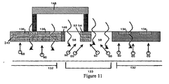
Figure 11 is a cross-sectional view of the imaging sensor employed in an LTF converter as shown inFigure 10 ; and -
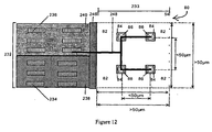
Figure 12 is a top plan view of an imaging sensor in accordance with the second embodiment of the invention employed in an LTF converter. - Since dark current originates from electron-hole pair generation in the depletion layer of a reverse biased junction and minority carrier diffusion/drift near the edge of the depletion region, the present invention reduces the dark current in an imaging sensor by reducing the interfacial area between its N-well and P-well components.
- Since the imaging sensor is designed for use in an LTF converter, for the sake of clarity, the imaging sensor will be referred to henceforth as an improved dynamic range LTF converter. Similarly, since the imaging sensor employed in the second embodiment employs multiple photodiodes in an LTF converter, the second embodiment will henceforth be known as a multiple photodiode improved dynamic range LTF converter.
- Referring to
Figures 9 and10 , the improved dynamicrange LTF converter 50 comprises an LTFconversion circuitry section 132 and a photo-generatedelectron collection section 133. The LTFconversion circuitry section 132 comprises N-MOS 134 and P-MOS 136 transistors embedded in a P-well 138 and N-well 140 material respectively. - Turning to the photo-generated
electron collection section 133, instead of using the large N-Well or N+ photodiodes of conventional LTF converters, the improved dynamicrange LTF converter 50 uses a small N-Well photodiode 52 (typically 5-10µm across) with a smallerN+ contact region 54 in its centre. - As in the previously described conventional LTF converter, the
photodiode 52 must be isolated from theLTF conversion circuitry 132 by a P-Well 146 or an N-well 56. However, referring toFigure 11 , in the improved dynamicrange LTF converter 50 the implantation of the P-Well 146 is suppressed, leaving the high resistivity P-epitaxial material 58. With this arrangement, photo-generatedcharge 60 will diffuse around the pixel and will probably be collected by the N-Well diode 52 especially since the operation of the LTF circuit renders the N-Well diode 52 the most positive node. For optimal photo-generated charge collection, the P-well 146 is connected to ground between the N-well 140 (biased positive at VDD) and the photo-generatedelectron collection section 133. - The diffusion length of electrons in the P-epitaxial substrates used in modern CMOS technology is typically 30µm-50µm. At distances greater than this, electrons are likely to recombine and be lost within the substrate. The improved LTF converter shown in
Figure 10 does not have this problem as thephotodiode 52 is smaller than 50µm. In addition, since the collection node (contact point) 54 is located in the centre of thephotodiode 52, the maximum length an electron has to diffuse before it reaches thecollection node 54 is (neglecting the size of the collection node)
- As discussed above, one method of increasing the sensitivity of an imaging sensor is to increase the size of its photodiodes. However, for pixels larger than approximately 50µm, the limited diffusion length of electrons in the P-epitaxial substrate prevents a significant proportion of photo-generated electrons from reaching a collection node.
-
Figure 12 shows a multiple photodiode improved dynamic range LTF converter that effectively permits the use of larger, more sensitive pixels. As in the conventional LTF converter, the multiple photodiode improved dynamicrange LTF converter 80 comprises an LTFconversion circuitry section 232 and a photo-generatedelectron collection section 233. As before, the LTFconversion circuitry section 232 comprises N-MOS 234 and P-MOS 236 transistors embedded in a P-well 238 and N-well 240 material respectively. However, the photo-generatedelectron collection section 233, comprises several regularly spaced (e.g. <50µm)collection nodes 82. In a similar fashion to the photodiodes shown inFigures 9-11 , each of thecollection nodes 82 uses asmall photodiode 84 from N-Well material (typically 5-10µm across) with a smallerN+ contact region 86 in its centre. - The 5µm-10µm collection nodes are connected together using a
metal conductor 248 that sums the photo-current. In addition, in a similar manner to conventional LTF converters, thephotodiodes 82 must be isolated from the LTFconversion circuitry section 232 by a P-Well 246. - By its nature, the improved dynamic range LTF converter can be readily included in an integrated circuit and is applicable to a broad range of devices including digital cameras, mobile phones incorporating a digital camera, and optical mice.
It will be appreciated that the man skilled in the art may employ standard techniques in order to implement the invention in these and other ways. - Improvements and modifications may be made to the above without departing from the scope of the invention.
Claims (27)
- An imaging sensor integrated circuit comprising a photo-current generating and collecting section (133) and a signal processing section (132), formed on a P-epitaxial material and separated from each other by a separating region (146, 56);
wherein the photo-current generating and collecting section (133) comprises an N-well (52) implant into the P-epitaxial material; and the N-well implant comprises an N+ contact (54); characterised in that
the separating region (146, 56) is implanted into the P-epitaxial material at substantially the same depth as the N-well implant (52);
and the N-well implant (52) is separated from the separating region (146, 56) by the P-epitaxial material (58), to form a photodiode PN junction between the N-well implant (52) and the P-epitaxial material (58). - The imaging sensor as claimed in Claim 1 wherein the separating region (146, 56) is an N-well (56).
- The imaging sensor as claimed in Claim 1 wherein the separating region (146, 56) is a P-well (146).
- The imaging sensor as claimed in any of the preceding Claims wherein the N-well implant (52) is of 5-10 µm in length.
- An imaging sensor integrated circuit comprising a photo-current generating and collecting section (133) and a signal processing section (132), formed on an N-epitaxial material and separated from each other by a separating region (146, 56);
wherein the photo-current generating and collecting section (133) comprises a P-well implant into the N-epitaxial material and the P-well implant comprises a P+ contact; characterised in that
the separating region is implanted into the N-epitaxial material at substantially the same depth as the P-well implant;
and the P-well implant is separated from the separating region by the N-epitaxial material to form a photodiode PN junction between the P-well implant and the N-epitaxial material. - The imaging sensor as claimed in Claim 5 wherein the P-well implant is of 5-10 µm in length.
- An imaging sensor integrated circuit comprising a photo-current generating and collecting section (133) and a signal processing section (132) formed on a P-epitaxial material and separated from each other by a separating region (146, 56);
wherein the photo-current generating and collecting section (133) comprises a plurality of N-well implants into the P-epitaxial material, each of the N-well implants comprising an N+ contact (54)
characterised in that the separating region (146,56) is implanted into the P-epitaxial material at substantially the same depth as the N-well implants (52) and the N-well implants (52) are separated from the separating region (146, 56) by the P-epitaxial material (58) to form a plurality of photodiode PN junctions between the N-well implants (52) and the P-epitaxial material (58). - The imaging sensor as claimed in Claim 7 wherein the separating region (146, 56) is an N-well.
- The imaging sensor as claimed in Claim 7 wherein the separating region (146, 56) is a P-well (246).
- The imaging sensor as claimed in any of Claims 7 to 9 wherein each of the plurality of N-well implants (84) is of 5-10 µm in length.
- The imaging sensor as claimed in any of Claims 7 to 10 wherein the plurality of N-well implants (84) are separated from each other by distances of less than 50µm.
- The imaging sensor as claimed in any of Claims 7 to 11 wherein the plurality of N-well implants (84) are connected together by a metal conductor (248).
- The imaging sensor as claimed in Claim 12 wherein the metal conductor (248) sums the photo-current received from the plurality of connected N-well implants (84).
- An imaging sensor integrated circuit comprising a photo-current generating and collection section (133) and a signal processing section (132) formed on an N-epitaxial material and separated from each other by a separating region (146,56);
wherein the photo-current generating and collecting section (133) comprises a plurality of P-well implants into the N-epitaxial material, each of the P-well implants comprising a P+ contact; characterised in that:the separating region is implanted into the N-epitaxial material at substantially the same depth as the P-well implants; andthe P-well implants are separated from the separating region by the N-epitaxial material to form a plurality of photodiode PN junctions between the P-well implants and the N-epitaxial material. - The imaging sensor as claimed in Claim 14 wherein each of the plurality of P-well implants is of 5-10 µm in length.
- The imaging sensor as claimed in Claim 14 or Claim 15 wherein the plurality of P-well implants are separated from each other by distances of less than 50µm.
- The imaging sensor as claimed in any of Claims 14 to 16 wherein the plurality of P-well implants are connected together by a metal conductor (248).
- The imaging sensor as claimed in Claim 17 wherein the metal conductor (248) sums the photo-current received from the plurality of connected P-well implants.
- The imaging sensor as claimed in any of the preceding Claims, wherein the signal processing section comprises a charge sensing amplifier (20).
- A light to frequency converter comprising an imaging sensor integrated circuit comprising a photo-current generating and collecting section (133) and a signal processing section (132), formed on a P-epitaxial material and separated from each other by a separating region (146, 56);
wherein the photo-current generating and collecting section (133) comprises an N-well (52) implant into the P-epitaxial material; and the N-well implant comprises an N+ contact (54)
characterised in that the separating region (146, 56) is implanted into the P-epitaxial material at substantially the same depth as the N-well implant (52); and the N-well implant (52) is separated from the separating region (146, 56) by the P-epitaxial material (58), to form a photodiode PN junction between the N-well implant (52) and the P-epitaxial material (58). - An optical mouse comprising an imaging sensor integrated circuit comprising a photo-current generating and collecting section (133) and a signal processing section (132), formed on a P-epitaxial material and separated from each other by a separating region (146, 56);
wherein the photo-current generating and collecting section (133) comprises an N-well (52) implant into the P-epitaxial material; and the N-well implant comprises an N+ contact (54)
characterised in that the separating region (146, 56) is implanted into the P-epitaxial material at substantially the same depth as the N-well implant (52); and the N-well implant (52) is separated from the separating region (146, 56) by the P-epitaxial material (58), to form a photodiode PN junction between the N-well implant (52) and the P-epitaxial material (58) - A digital camera comprising an imaging sensor integrated circuit comprising a photo-current generating and collecting section (133) and a signal processing section (132), formed on a P-epitaxial material and separated from each other by a separating region (146, 56);
wherein the photo-current generating and collecting section (133) comprises an N-well (52) implant into the P-epitaxial material; and an the N-well implant comprises an N+ contact (54)
characterised in that the separating region (146, 56) is implanted into the P-epitaxial material at substantially the same depth as the N-well implant (52); and the N-well implant (52) is separated from the separating region (146, 56) by the P-epitaxial material (58), so as to form a photodiode PN junction between the N-well implant (52) and the P-epitaxial material (58) - A mobile phone comprising the digital camera as claimed in Claim 22.
- A light to frequency converter comprising an imaging sensor integrated circuit comprising a photo-current generating and collecting section (133) and a signal processing section (132), formed on an N-epitaxial material and separated from each other by a separating region (146, 56);
wherein the photo-current generating and collecting section (133) comprises a P-well implant into the N-epitaxial material and the P-well implant comprisesa P+ contact; characterised in that
the separating region is implanted into the N-epitaxial material at substantially the same depth as the P-well implant;
and the P-well implant is separated from the separating region by the N-epitaxial material to form a photodiode PN junction between the P-well implant and the N-epitaxial material. - An optical mouse comprising an imaging sensor integrated circuit comprising a photo-current generating and collecting section (133) and a signal processing section (132), formed on an N-epitaxial material and separated from each other by a separating region (146, 56);
wherein the photo-current generating and collecting section (133) comprises a P-well implant into the N-epitaxial material and the P-well implant comprisesa P+ contact; characterised in that
the separating region is implanted into the N-epitaxial material at substantially the same depth as the P-well implant;
and the P-well implant is separated from the separating region by the N-epitaxial material to form a photodiode PN junction between the P-well implant and the N-epitaxial material. - A digital camera comprising an imaging sensor integrated circuit comprising a photo-current generating and collecting section (133) and a signal processing section (132), formed on an N-epitaxial material and separated from each other by a separating region (146, 56);
wherein the photo-current generating and collecting section (133) comprises a P-well implant into the N-epitaxial material and the P-well implant comprisesa P+ contact; characterised in that the separating region is implanted into the N-epitaxial material at substantially the same depth as the P-well implant;
and the P-well implant is separated from the separating region by the N-epitaxial material to form a photodiode PN junction between the P-well implant and the N-epitaxial material. - A mobile phone comprising the digital camera as claimed in Claim 26.
Priority Applications (3)
| Application Number | Priority Date | Filing Date | Title |
|---|---|---|---|
| EP04253557A EP1608019B1 (en) | 2004-06-15 | 2004-06-15 | Imaging sensor |
| DE602004025681T DE602004025681D1 (en) | 2004-06-15 | 2004-06-15 | image sensor |
| US11/148,930 US7358584B2 (en) | 2004-06-15 | 2005-06-09 | Imaging sensor |
Applications Claiming Priority (1)
| Application Number | Priority Date | Filing Date | Title |
|---|---|---|---|
| EP04253557A EP1608019B1 (en) | 2004-06-15 | 2004-06-15 | Imaging sensor |
Publications (2)
| Publication Number | Publication Date |
|---|---|
| EP1608019A1 EP1608019A1 (en) | 2005-12-21 |
| EP1608019B1 true EP1608019B1 (en) | 2010-02-24 |
Family
ID=34930405
Family Applications (1)
| Application Number | Title | Priority Date | Filing Date |
|---|---|---|---|
| EP04253557A Expired - Lifetime EP1608019B1 (en) | 2004-06-15 | 2004-06-15 | Imaging sensor |
Country Status (3)
| Country | Link |
|---|---|
| US (1) | US7358584B2 (en) |
| EP (1) | EP1608019B1 (en) |
| DE (1) | DE602004025681D1 (en) |
Families Citing this family (2)
| Publication number | Priority date | Publication date | Assignee | Title |
|---|---|---|---|---|
| DE102009052159A1 (en) | 2009-08-05 | 2011-02-10 | Georg Fritzmeier Gmbh & Co. Kg | Measuring device for determining a vegetation index value (REIP) of plants |
| GB0921944D0 (en) * | 2009-12-16 | 2010-02-03 | St Microelectronics Ltd | Improvements in or relating to compact fluorescent lamps |
Family Cites Families (12)
| Publication number | Priority date | Publication date | Assignee | Title |
|---|---|---|---|---|
| US4696021A (en) * | 1982-06-03 | 1987-09-22 | Nippon Kogaku K.K. | Solid-state area imaging device having interline transfer CCD means |
| JPS62269357A (en) * | 1986-05-19 | 1987-11-21 | Sony Corp | Solid-state image sensing device |
| US5850195A (en) * | 1993-09-09 | 1998-12-15 | Texas Instruments Incorporated | Monolithic light-to-digital signal converter |
| JP3467858B2 (en) * | 1993-11-02 | 2003-11-17 | ソニー株式会社 | Photoelectric conversion element |
| JPH09260715A (en) * | 1996-03-25 | 1997-10-03 | Sanyo Electric Co Ltd | Photodiode built-in semiconductor integrated circuit |
| JP3457551B2 (en) * | 1998-11-09 | 2003-10-20 | 株式会社東芝 | Solid-state imaging device |
| JP2002203954A (en) * | 2000-10-31 | 2002-07-19 | Sharp Corp | Photodetector with built-in circuit |
| DE60216046D1 (en) * | 2002-04-18 | 2006-12-28 | Sgs Thomson Microelectronics | Semiconductor structure |
| US7064406B2 (en) * | 2003-09-03 | 2006-06-20 | Micron Technology, Inc. | Supression of dark current in a photosensor for imaging |
| KR100535926B1 (en) * | 2003-09-22 | 2005-12-09 | 동부아남반도체 주식회사 | Method for Manufacturing CMOS Image Sensor |
| KR100558530B1 (en) * | 2003-09-23 | 2006-03-10 | 동부아남반도체 주식회사 | CMOS image sensor and its manufacturing method |
| US7193257B2 (en) * | 2004-01-29 | 2007-03-20 | Victor Company Of Japan, Ltd. | Solid state image sensing device and manufacturing and driving methods thereof |
-
2004
- 2004-06-15 EP EP04253557A patent/EP1608019B1/en not_active Expired - Lifetime
- 2004-06-15 DE DE602004025681T patent/DE602004025681D1/en not_active Expired - Lifetime
-
2005
- 2005-06-09 US US11/148,930 patent/US7358584B2/en not_active Expired - Lifetime
Also Published As
| Publication number | Publication date |
|---|---|
| DE602004025681D1 (en) | 2010-04-08 |
| US7358584B2 (en) | 2008-04-15 |
| US20050275052A1 (en) | 2005-12-15 |
| EP1608019A1 (en) | 2005-12-21 |
Similar Documents
| Publication | Publication Date | Title |
|---|---|---|
| EP1883966B1 (en) | Pinned-photodiode pixel with global shutter | |
| US6424375B1 (en) | Low noise active reset readout for image sensors | |
| US5608243A (en) | Single split-gate MOS transistor active pixel sensor cell with automatic anti-blooming and wide dynamic range | |
| US5587596A (en) | Single MOS transistor active pixel sensor cell with automatic anti-blooming and wide dynamic range | |
| US6982183B2 (en) | Method and system for manufacturing a pixel image sensor | |
| EP1032049B1 (en) | Photoelectric converting element | |
| EP0854516A2 (en) | Partially pinned photodiode for solid state image sensors | |
| US6815791B1 (en) | Buried, fully depletable, high fill factor photodiodes | |
| JP2000082839A (en) | Photodiode, unit pixel of image sensor using the same, and method of obtaining data therefrom | |
| TWI294188B (en) | Active pixel cell using asymmetric transfer transistor | |
| KR101818587B1 (en) | Unit pixel, photo-detection device and method of measuring a distance using the same | |
| CN100502023B9 (en) | Using the active pixel cell of asymmetric transmission transistor | |
| Park et al. | Simultaneous imaging and energy harvesting in CMOS image sensor pixels | |
| KR101905979B1 (en) | Image sensor with solar cell function and electronic device thereof | |
| US20020093015A1 (en) | Solid-state image sensor provided with divided photoelectric conversion part | |
| JP2001326343A (en) | Solid-state imaging device | |
| US7358584B2 (en) | Imaging sensor | |
| US20070284507A1 (en) | Variably responsive photosensor | |
| KR100333723B1 (en) | image sensor having on-transfer photodiode and data read out method of the same | |
| CN119012035A (en) | Pixel unit, dynamic vision sensor and electronic equipment | |
| CN108848327A (en) | Silicon substrate blendes together CMOS-APD image sensor system | |
| JP2001237407A (en) | Electromagnetic radiation detector and method of manufacturing the same | |
| EP4637172A1 (en) | Pixel coupling | |
| Liu et al. | Silicon CMOS Image Sensor With Wide Response Spectrum From 254 nm to 1310 nm Enabled by Photodiode-Body-Biased MOSFET | |
| JPH1022489A (en) | Solid-state image pickup device |
Legal Events
| Date | Code | Title | Description |
|---|---|---|---|
| PUAI | Public reference made under article 153(3) epc to a published international application that has entered the european phase |
Free format text: ORIGINAL CODE: 0009012 |
|
| AK | Designated contracting states |
Kind code of ref document: A1 Designated state(s): AT BE BG CH CY CZ DE DK EE ES FI FR GB GR HU IE IT LI LU MC NL PL PT RO SE SI SK TR |
|
| AX | Request for extension of the european patent |
Extension state: AL HR LT LV MK |
|
| 17P | Request for examination filed |
Effective date: 20060606 |
|
| AKX | Designation fees paid |
Designated state(s): DE FR GB IT |
|
| 17Q | First examination report despatched |
Effective date: 20070726 |
|
| RAP1 | Party data changed (applicant data changed or rights of an application transferred) |
Owner name: STMICROELECTRONICS (RESEARCH & DEVELOPMENT) LIMITE |
|
| GRAP | Despatch of communication of intention to grant a patent |
Free format text: ORIGINAL CODE: EPIDOSNIGR1 |
|
| GRAS | Grant fee paid |
Free format text: ORIGINAL CODE: EPIDOSNIGR3 |
|
| GRAA | (expected) grant |
Free format text: ORIGINAL CODE: 0009210 |
|
| AK | Designated contracting states |
Kind code of ref document: B1 Designated state(s): DE FR GB IT |
|
| REG | Reference to a national code |
Ref country code: GB Ref legal event code: FG4D |
|
| REF | Corresponds to: |
Ref document number: 602004025681 Country of ref document: DE Date of ref document: 20100408 Kind code of ref document: P |
|
| PLBE | No opposition filed within time limit |
Free format text: ORIGINAL CODE: 0009261 |
|
| STAA | Information on the status of an ep patent application or granted ep patent |
Free format text: STATUS: NO OPPOSITION FILED WITHIN TIME LIMIT |
|
| 26N | No opposition filed |
Effective date: 20101125 |
|
| PG25 | Lapsed in a contracting state [announced via postgrant information from national office to epo] |
Ref country code: IT Free format text: LAPSE BECAUSE OF FAILURE TO SUBMIT A TRANSLATION OF THE DESCRIPTION OR TO PAY THE FEE WITHIN THE PRESCRIBED TIME-LIMIT Effective date: 20100224 |
|
| REG | Reference to a national code |
Ref country code: FR Ref legal event code: PLFP Year of fee payment: 13 |
|
| REG | Reference to a national code |
Ref country code: FR Ref legal event code: PLFP Year of fee payment: 14 |
|
| REG | Reference to a national code |
Ref country code: FR Ref legal event code: PLFP Year of fee payment: 15 |
|
| PGFP | Annual fee paid to national office [announced via postgrant information from national office to epo] |
Ref country code: FR Payment date: 20230523 Year of fee payment: 20 Ref country code: DE Payment date: 20230523 Year of fee payment: 20 |
|
| PGFP | Annual fee paid to national office [announced via postgrant information from national office to epo] |
Ref country code: GB Payment date: 20230523 Year of fee payment: 20 |
|
| REG | Reference to a national code |
Ref country code: DE Ref legal event code: R071 Ref document number: 602004025681 Country of ref document: DE |
|
| PG25 | Lapsed in a contracting state [announced via postgrant information from national office to epo] |
Ref country code: GB Free format text: LAPSE BECAUSE OF EXPIRATION OF PROTECTION Effective date: 20240614 |
|
| PG25 | Lapsed in a contracting state [announced via postgrant information from national office to epo] |
Ref country code: GB Free format text: LAPSE BECAUSE OF EXPIRATION OF PROTECTION Effective date: 20240614 |