EP1607928A2 - Device and method for driving display panel - Google Patents
Device and method for driving display panel Download PDFInfo
- Publication number
- EP1607928A2 EP1607928A2 EP05012759A EP05012759A EP1607928A2 EP 1607928 A2 EP1607928 A2 EP 1607928A2 EP 05012759 A EP05012759 A EP 05012759A EP 05012759 A EP05012759 A EP 05012759A EP 1607928 A2 EP1607928 A2 EP 1607928A2
- Authority
- EP
- European Patent Office
- Prior art keywords
- display
- subfields
- display line
- pixel data
- pixel
- Prior art date
- Legal status (The legal status is an assumption and is not a legal conclusion. Google has not performed a legal analysis and makes no representation as to the accuracy of the status listed.)
- Withdrawn
Links
Images



Classifications
-
- G—PHYSICS
- G09—EDUCATION; CRYPTOGRAPHY; DISPLAY; ADVERTISING; SEALS
- G09G—ARRANGEMENTS OR CIRCUITS FOR CONTROL OF INDICATING DEVICES USING STATIC MEANS TO PRESENT VARIABLE INFORMATION
- G09G3/00—Control arrangements or circuits, of interest only in connection with visual indicators other than cathode-ray tubes
- G09G3/20—Control arrangements or circuits, of interest only in connection with visual indicators other than cathode-ray tubes for presentation of an assembly of a number of characters, e.g. a page, by composing the assembly by combination of individual elements arranged in a matrix no fixed position being assigned to or needed to be assigned to the individual characters or partial characters
- G09G3/22—Control arrangements or circuits, of interest only in connection with visual indicators other than cathode-ray tubes for presentation of an assembly of a number of characters, e.g. a page, by composing the assembly by combination of individual elements arranged in a matrix no fixed position being assigned to or needed to be assigned to the individual characters or partial characters using controlled light sources
- G09G3/28—Control arrangements or circuits, of interest only in connection with visual indicators other than cathode-ray tubes for presentation of an assembly of a number of characters, e.g. a page, by composing the assembly by combination of individual elements arranged in a matrix no fixed position being assigned to or needed to be assigned to the individual characters or partial characters using controlled light sources using luminous gas-discharge panels, e.g. plasma panels
- G09G3/288—Control arrangements or circuits, of interest only in connection with visual indicators other than cathode-ray tubes for presentation of an assembly of a number of characters, e.g. a page, by composing the assembly by combination of individual elements arranged in a matrix no fixed position being assigned to or needed to be assigned to the individual characters or partial characters using controlled light sources using luminous gas-discharge panels, e.g. plasma panels using AC panels
- G09G3/291—Control arrangements or circuits, of interest only in connection with visual indicators other than cathode-ray tubes for presentation of an assembly of a number of characters, e.g. a page, by composing the assembly by combination of individual elements arranged in a matrix no fixed position being assigned to or needed to be assigned to the individual characters or partial characters using controlled light sources using luminous gas-discharge panels, e.g. plasma panels using AC panels controlling the gas discharge to control a cell condition, e.g. by means of specific pulse shapes
- G09G3/293—Control arrangements or circuits, of interest only in connection with visual indicators other than cathode-ray tubes for presentation of an assembly of a number of characters, e.g. a page, by composing the assembly by combination of individual elements arranged in a matrix no fixed position being assigned to or needed to be assigned to the individual characters or partial characters using controlled light sources using luminous gas-discharge panels, e.g. plasma panels using AC panels controlling the gas discharge to control a cell condition, e.g. by means of specific pulse shapes for address discharge
- G09G3/2935—Addressed by erasing selected cells that are in an ON state
-
- G—PHYSICS
- G09—EDUCATION; CRYPTOGRAPHY; DISPLAY; ADVERTISING; SEALS
- G09G—ARRANGEMENTS OR CIRCUITS FOR CONTROL OF INDICATING DEVICES USING STATIC MEANS TO PRESENT VARIABLE INFORMATION
- G09G3/00—Control arrangements or circuits, of interest only in connection with visual indicators other than cathode-ray tubes
- G09G3/20—Control arrangements or circuits, of interest only in connection with visual indicators other than cathode-ray tubes for presentation of an assembly of a number of characters, e.g. a page, by composing the assembly by combination of individual elements arranged in a matrix no fixed position being assigned to or needed to be assigned to the individual characters or partial characters
- G09G3/2007—Display of intermediate tones
- G09G3/2018—Display of intermediate tones by time modulation using two or more time intervals
- G09G3/2022—Display of intermediate tones by time modulation using two or more time intervals using sub-frames
-
- G—PHYSICS
- G09—EDUCATION; CRYPTOGRAPHY; DISPLAY; ADVERTISING; SEALS
- G09G—ARRANGEMENTS OR CIRCUITS FOR CONTROL OF INDICATING DEVICES USING STATIC MEANS TO PRESENT VARIABLE INFORMATION
- G09G3/00—Control arrangements or circuits, of interest only in connection with visual indicators other than cathode-ray tubes
- G09G3/20—Control arrangements or circuits, of interest only in connection with visual indicators other than cathode-ray tubes for presentation of an assembly of a number of characters, e.g. a page, by composing the assembly by combination of individual elements arranged in a matrix no fixed position being assigned to or needed to be assigned to the individual characters or partial characters
- G09G3/2007—Display of intermediate tones
- G09G3/2044—Display of intermediate tones using dithering
- G09G3/2051—Display of intermediate tones using dithering with use of a spatial dither pattern
-
- G—PHYSICS
- G09—EDUCATION; CRYPTOGRAPHY; DISPLAY; ADVERTISING; SEALS
- G09G—ARRANGEMENTS OR CIRCUITS FOR CONTROL OF INDICATING DEVICES USING STATIC MEANS TO PRESENT VARIABLE INFORMATION
- G09G3/00—Control arrangements or circuits, of interest only in connection with visual indicators other than cathode-ray tubes
- G09G3/20—Control arrangements or circuits, of interest only in connection with visual indicators other than cathode-ray tubes for presentation of an assembly of a number of characters, e.g. a page, by composing the assembly by combination of individual elements arranged in a matrix no fixed position being assigned to or needed to be assigned to the individual characters or partial characters
- G09G3/2007—Display of intermediate tones
- G09G3/2059—Display of intermediate tones using error diffusion
-
- G—PHYSICS
- G09—EDUCATION; CRYPTOGRAPHY; DISPLAY; ADVERTISING; SEALS
- G09G—ARRANGEMENTS OR CIRCUITS FOR CONTROL OF INDICATING DEVICES USING STATIC MEANS TO PRESENT VARIABLE INFORMATION
- G09G3/00—Control arrangements or circuits, of interest only in connection with visual indicators other than cathode-ray tubes
- G09G3/20—Control arrangements or circuits, of interest only in connection with visual indicators other than cathode-ray tubes for presentation of an assembly of a number of characters, e.g. a page, by composing the assembly by combination of individual elements arranged in a matrix no fixed position being assigned to or needed to be assigned to the individual characters or partial characters
- G09G3/2007—Display of intermediate tones
- G09G3/2077—Display of intermediate tones by a combination of two or more gradation control methods
-
- G—PHYSICS
- G09—EDUCATION; CRYPTOGRAPHY; DISPLAY; ADVERTISING; SEALS
- G09G—ARRANGEMENTS OR CIRCUITS FOR CONTROL OF INDICATING DEVICES USING STATIC MEANS TO PRESENT VARIABLE INFORMATION
- G09G3/00—Control arrangements or circuits, of interest only in connection with visual indicators other than cathode-ray tubes
- G09G3/20—Control arrangements or circuits, of interest only in connection with visual indicators other than cathode-ray tubes for presentation of an assembly of a number of characters, e.g. a page, by composing the assembly by combination of individual elements arranged in a matrix no fixed position being assigned to or needed to be assigned to the individual characters or partial characters
- G09G3/22—Control arrangements or circuits, of interest only in connection with visual indicators other than cathode-ray tubes for presentation of an assembly of a number of characters, e.g. a page, by composing the assembly by combination of individual elements arranged in a matrix no fixed position being assigned to or needed to be assigned to the individual characters or partial characters using controlled light sources
- G09G3/28—Control arrangements or circuits, of interest only in connection with visual indicators other than cathode-ray tubes for presentation of an assembly of a number of characters, e.g. a page, by composing the assembly by combination of individual elements arranged in a matrix no fixed position being assigned to or needed to be assigned to the individual characters or partial characters using controlled light sources using luminous gas-discharge panels, e.g. plasma panels
- G09G3/2803—Display of gradations
-
- G—PHYSICS
- G09—EDUCATION; CRYPTOGRAPHY; DISPLAY; ADVERTISING; SEALS
- G09G—ARRANGEMENTS OR CIRCUITS FOR CONTROL OF INDICATING DEVICES USING STATIC MEANS TO PRESENT VARIABLE INFORMATION
- G09G3/00—Control arrangements or circuits, of interest only in connection with visual indicators other than cathode-ray tubes
- G09G3/20—Control arrangements or circuits, of interest only in connection with visual indicators other than cathode-ray tubes for presentation of an assembly of a number of characters, e.g. a page, by composing the assembly by combination of individual elements arranged in a matrix no fixed position being assigned to or needed to be assigned to the individual characters or partial characters
- G09G3/22—Control arrangements or circuits, of interest only in connection with visual indicators other than cathode-ray tubes for presentation of an assembly of a number of characters, e.g. a page, by composing the assembly by combination of individual elements arranged in a matrix no fixed position being assigned to or needed to be assigned to the individual characters or partial characters using controlled light sources
- G09G3/28—Control arrangements or circuits, of interest only in connection with visual indicators other than cathode-ray tubes for presentation of an assembly of a number of characters, e.g. a page, by composing the assembly by combination of individual elements arranged in a matrix no fixed position being assigned to or needed to be assigned to the individual characters or partial characters using controlled light sources using luminous gas-discharge panels, e.g. plasma panels
- G09G3/288—Control arrangements or circuits, of interest only in connection with visual indicators other than cathode-ray tubes for presentation of an assembly of a number of characters, e.g. a page, by composing the assembly by combination of individual elements arranged in a matrix no fixed position being assigned to or needed to be assigned to the individual characters or partial characters using controlled light sources using luminous gas-discharge panels, e.g. plasma panels using AC panels
- G09G3/291—Control arrangements or circuits, of interest only in connection with visual indicators other than cathode-ray tubes for presentation of an assembly of a number of characters, e.g. a page, by composing the assembly by combination of individual elements arranged in a matrix no fixed position being assigned to or needed to be assigned to the individual characters or partial characters using controlled light sources using luminous gas-discharge panels, e.g. plasma panels using AC panels controlling the gas discharge to control a cell condition, e.g. by means of specific pulse shapes
- G09G3/293—Control arrangements or circuits, of interest only in connection with visual indicators other than cathode-ray tubes for presentation of an assembly of a number of characters, e.g. a page, by composing the assembly by combination of individual elements arranged in a matrix no fixed position being assigned to or needed to be assigned to the individual characters or partial characters using controlled light sources using luminous gas-discharge panels, e.g. plasma panels using AC panels controlling the gas discharge to control a cell condition, e.g. by means of specific pulse shapes for address discharge
- G09G3/2932—Addressed by writing selected cells that are in an OFF state
-
- G—PHYSICS
- G09—EDUCATION; CRYPTOGRAPHY; DISPLAY; ADVERTISING; SEALS
- G09G—ARRANGEMENTS OR CIRCUITS FOR CONTROL OF INDICATING DEVICES USING STATIC MEANS TO PRESENT VARIABLE INFORMATION
- G09G2340/00—Aspects of display data processing
- G09G2340/04—Changes in size, position or resolution of an image
- G09G2340/0407—Resolution change, inclusive of the use of different resolutions for different screen areas
- G09G2340/0428—Gradation resolution change
Definitions
- the present invention relates to a drive device and a drive method for driving a display panel such as a plasma display panel.
- a plasma display panel (hereinafter referred to as a PDP) has received attention.
- the PDP is directly driven by a digital video signal, and gray scale of luminance which the PDP can represent is determined by bit number of pixel data of each pixel on the basis of the above digital video signal.
- a subfield method in which a unit frame display period, for example, one field (one frame) display period is divided into subfields of N-number, of which each emits light for only time corresponding to a weight of each bit digit of pixel data (N bits), thereby to drive the PDP.
- the field takes a video signal of interlaced type such as NTSC into consideration, and in a video signal of non-interlaced type, the field corresponds to a frame.
- one filed display period is divided into 8 subfields comprising subfields SF8, SF7, ⁇ , SF1 in order of a weight.
- Each of the subfields has an address period in which setting of a lit pixel and a unlit pixel according to pixel data is performed for each display line of the PDP, and a sustain period in which only the lit pixel is caused to emit light for only time corresponding to a weight of its subfield.
- light-emission drive control determining whether light emission is executed or not in its subfield is individually performed. Therefore, in one field, subfields in a "light emission state" and subfields in a "non-light emission state” are mixed. At this time, by total time of light emission executed in each subfield in one filed, a halftone luminance is represented.
- the gradation drive uses dither processing together, thereby to increase the gray scale visually and improve image quality.
- one halftone luminance is represented. For example, with four pixels adjacent to each other up and down and right and left forming a set, four dither values (for example, 0, 1, 2, and 3) composed of values (added value) different to each other are assigned to pixel data corresponding to each of this set of pixels, and added to each pixel data.
- four dither values for example, 0, 1, 2, and 3
- values (added value) different to each other are assigned to pixel data corresponding to each of this set of pixels, and added to each pixel data.
- a display panel driving device is a device for driving a display panel which has n (n is a natural number) display lines and pixel cells carrying pixels for each of the n display lines, and in order to display a halftone image in a one-field display period of a video signal which is divided into the plurality of subfields, for performing address scanning for changing each of the pixel cells from a lit mode to an unlit mode in one of the plurality of subfields in accordance with image data based on the video signal, a predetermined number of continuous subfields in one field each being formed by M divided subfields and the n display lines being divided into M display line groups for each display lines, the device comprising: data converting means for applying data conversion to pixel data corresponding to each of the M display line groups with a different conversion characteristic from each other; a multi-gradation processing unit for applying multi-gradation processing to the pixel data subjected to the data conversion; and a gradation drive unit for performing the address scanning for changing each of the pixel cells from
- a display panel driving method is a method for driving a display panel which has n (n is a natural number) display lines and pixel cells carrying pixels for each of the n display lines, and in order to display a halftone image in a one-field display period of a video signal which is divided into the plurality of subfields, for performing address scanning for changing each of the pixel cells from a lit mode to an unlit mode in one of the plurality of subfields in accordance with image data based on the video signal, a predetermined number of continuous subfields in one field each being formed by M divided subfields and the n display lines being divided into M display line groups for each display lines, the method comprising: a step of applying data conversion to pixel data corresponding to each of the M display line groups with a different conversion characteristic from each other; a step of applying multi-gradation processing to the pixel data subjected to the data conversion; and a step of performing the address scanning for changing each of the pixel cells from the lit mode to the unlit mode in accord
- a display panel driving device is a device for driving a display panel which has a plurality of display lines and pixel cells carrying pixels for each of the plurality of display lines, so as to display a halftone image in accordance with image data based on the video signal, the device comprising: a data converting unit for applying, for each display line group including p (p is a natural number equal to or larger than two) display lines adjacent to one another, data conversion to pixel data corresponding to each of the p display lines with a different conversion characteristic from each other for each of the display lines; a multi-gradation processing unit for applying multi-gradation processing to the pixel data subjected to the data conversion; and light emission driving means for allowing the pixel cells to emit light in accordance with the pixel data subjected to the multi-gradation processing with a luminance weight different from each other given to each of the display line groups.
- a display panel driving method is a method for driving a display panel which has a plurality of display lines and pixel cells carrying pixels for each of the plurality of display lines, so as to display a halftone image in accordance with image data based on the video signal, the method comprising: a step of applying, for each display line group including p (p is a natural number equal to or larger than two) display lines adjacent to one another, data conversion to pixel data corresponding to each of the p display lines with a different conversion characteristic from each other for each of the display lines; a step of applying multi-gradation processing to the pixel data subjected to the data conversion; and a step of allowing the pixel cells to emit light in accordance with the pixel data subjected to the multi-gradation processing with a luminance weight different from each other given to each of the display line groups.
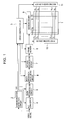
- Fig. 1 shows a schematic structure of a plasma display apparatus according to the present invention.
- the plasma display apparatus has a PDP 1 serving as a plasma display panel.
- the plasma display apparatus includes a synchronization detection circuit 2, a drive control circuit 3, an A/D converter 4, a data conversion circuit 5, a multi-gradation processing circuit 6, an SF data conversion circuit 7, a frame memory 8, an address driver 9, a first sustain driver 10, and a second sustain driver 11 that are used for driving the PDP 1.
- the PDP 1 includes column electrodes D 1 to D m serving as address electrodes and row electrodes X 1 to X n and row electrodes Y 1 to Y n that are arranged orthogonal to the column electrodes.
- a pair of the row electrode X and the row Y forms a row electrode corresponding to an electrode for one row.
- the row electrode pairs and the column electrodes are covered by a dielectric layer against a discharge space.
- Discharge cells corresponding to pixels are formed at intersections of the respective row electrode pairs and the respective column electrodes.
- N display lines form four display line groups.
- a first display line group includes a 4k-3rd line
- a second display line group includes a 4k-2nd line
- a third display line group includes a 4k-1st line
- a fourth display line group includes a 4kth line.
- K is an integer equal to or larger than 1.
- the synchronization detection circuit 2 generates a vertical synchronization signal V when the synchronization detection circuit 2 detects a vertical synchronization signal V out of video signals serving as unit frame information signals that are continuously supplied for each frame. Moreover, the synchronization detection circuit 2 generates a horizontal synchronization signal H when the synchronization detection circuit 2 detects a horizontal synchronization signal H out of the video signals. The synchronization detection circuit 2 supplies the vertical synchronization signal V and the horizontal synchronization signal H to the drive control circuit 3 and the data conversion circuit 5.
- the A/D converter 4 samples a video signal out of the video signals in accordance with a clock signal supplied from the drive control circuit 3, converts the video signal into 8-bit pixel data D indicating luminance from "0" to "255" for each pixel, and supplies the pixel data D to the data conversion circuit 5.
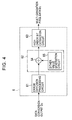
- the data conversion circuit 5 includes first to fourth data conversion circuits 51 to 54 and a selector 55.
- the pixel data D is supplied to the first to the fourth data conversion circuits 51 to 54.
- the first to the fourth data conversion circuits 51 to 54 have conversion characteristics different from one another.
- the first to the fourth data conversion circuits 51 to 54 converts the pixel data D into 8-bit converted pixel data D H from "0" to "255".
- the first data conversion circuit 51 is a data conversion circuit for the first display line group 4k-3
- the second data conversion circuit 52 is a data conversion circuit for the second display line group 4k-2
- the third data conversion circuit 53 is a data conversion circuit for the third display line group 4k-1
- the fourth data conversion circuit 54 is a data conversion circuit for the fourth display line group 4k.
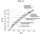
- Conversion characteristics of the first to the fourth data conversion circuits 51 to 54 are determined taking into account actual visual characteristics.
- the first to the fourth data conversion circuits 51 to 54 have characteristics obtained by subjecting a signal between subfields described later to gamma correction (raising subfields to the power of 2.2).
- a relation between an input value x and an output value y of the first to the fourth data conversion circuits 51 to 54 can be represented by the following expression.
- the selector 55 selects and outputs one output data of the output pixel data DH of the first to the fourth data conversion circuits 51 to 54 in accordance with an instruction of the drive control circuit 3.
- the multi-gradation processing circuit 6 includes an error diffusion processing circuit 61, a dither processing circuit 62, and a high order bit extraction circuit 63.
- the dither processing circuit 62 includes an adder 64 and a dither value generation circuit 65.
- the multi-gradation processing circuit 6 applies error diffusion processing and dither processing to the 8-bit converted pixel data D H to thereby generate multi-gradation processing pixel data D S obtained by reducing the number of bits to three while maintaining the number of gradations.
- the error diffusion processing circuit 61 recognizes a high order six bits of the pixel data D H as display data and recognizes the remaining low order two bits of the pixel data D H as error data. Then, the error diffusion processing circuit 61 reflects error data, which is obtained by weighting and adding respective error data of the pixel data D H corresponding to respective peripheral pixels, on the display data. Through such an operation, luminance for the lower two bits in the original pixels is represented simulatively by the peripheral pixels.
- the multi-gradation processing circuit 6 applies the dither processing to 6-bit error diffusion processing pixel data obtained by the error diffusion processing.
- the dither value generation circuit 65 generates dither values different from each other for the respective error diffusion processing pixel data corresponding to the respective pixels in this one pixel group.
- the adder 64 adds the dither values and the error diffusion processing pixel data to obtain dither added pixel data.
- the high order bit extraction circuit 63 supplies the high order three bits of the dither added pixel data to the SF data conversion circuit 7 as the multi-gradation pixel data D S .
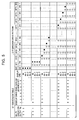
- the SF data conversion circuit 7 converts the multi-gradation pixel data D S for the high order three bits into display drive pixel data GD consisting of eight bits in accordance with a conversion table shown in Fig. 5.
- the respective eight bits correspond to subfields SF0 to SF7 described later in order of bit.
- the frame memory 8 sequentially writes and stores the display drive pixel data GD therein in accordance with a writing signal supplied from the drive control circuit 3. According to the writing operation, GD 11 to GD nm are written as display drive pixel data for one frame (n rows and m columns). When the writing ends, the frame memory 8 sequentially reads out the display drive pixel data GD 11 to GD nm for the same bit digit and for each row in accordance with a readout signal supplied from the drive control circuit 3 and supplies the display drive pixel data GD 11 to GD nm to the address driver 9.
- the frame memory 8 reads out the display drive pixel data GD 11 to GD nm for one frame, each consisting of eight bits, as display drive pixel data bits DB1 11 to DB8 nm that are obtained by dividing the display drive pixel data GD 11 to GD nm into eight in the following manner.
- DB1 11 to DB1 nm first bit of the display drive pixel data GD 11 to GD nm DB2 11 to DB2 nm : second bit of the display drive pixel data GD 11 to GD nm DB3 11 to DB3 nm : third bit of the display drive pixel data GD 11 to GD nm DB4 11 to DB4 nm : fourth bit of the display drive pixel data GD 11 to GD nm DB5 11 to DB5 nm : fifth bit of the display drive pixel data GD 11 to GD nm DB6 11 to DB6 nm : sixth bit of the display drive pixel data GD 11 to GD nm DB7 11 to DB7 nm : seventh bit of the display drive pixel data GD 11 to GD nm DB8 11 to DB8 nm : eighth bit of the display drive pixel data GD 11 to GD nm : eighth bit of the display drive
- These display drive pixel data bits DB1 11 to DB1 nm , DB2 11 to DB2 nm , ..., DB8 11 to DB8 nm are sequentially read out for each row in accordance with a readout signal supplied from the drive control circuit 3 and supplied to the address driver 9.
- the drive control circuit 3 generates a clock signal to be supplied to the A/D converter 4 and writing and readout signals to be supplied to the frame memory 8 in synchronization with the horizontal synchronization signal H and the vertical synchronization signal V.
- the drive control circuit 3 supplies various timing signals for driving the PDP 1 to the address driver 9, the first sustain driver 10, and the second sustain driver 11 in accordance with a light emission drive format shown in Fig. 6.
- a display period for one field is divided into subfields SF0 to SF8.
- the subfields SF2 to SF7 include four subfields SF21 to SF24, SF31 to SF34, ..., SF71 to SF74, respectively.
- Various drive steps are carried out for each of the subfields as described below.
- a reset step R of initializing all discharge cells of the PDP 1 to a lit mode (a state in which a predetermined amount of wall charge is formed) is executed.
- address step W0 of changing the respective discharge cells to an unlit mode (a state in which a wall charge is erased) selectively is executed on all display lines in accordance with the pixel drive data.
- a sustain step I of causing only the discharge cells in the lit mode to discharge and emit light is executed.
- an address step W0 of changing the respective discharge cells to the unlit mode selectively is executed on all the display lines in accordance with the pixel drive data.
- the sustain step I of causing only the discharge cells in the lit mode to discharge and emit light is executed in accordance with a result of the address step W0 in the subfield SF1.
- an address step W1 of changing the respective discharge cells, which belong to the 4kth display line, to the unlit mode selectively is executed in accordance with pixel drive data.
- the sustain step I of causing only the discharge cells in the lit mode is executed in accordance with results of the address step W1 in the subfield SF21 for the 4kth display line and the address step W0 of the subfield SF1 for the other display lines.
- an address step W2 for changing the respective discharge cells, which belong to the 4k-1st display line, to the unlit mode selectively is executed in accordance with pixel drive data.
- the sustain step I of causing only the discharge cells in the lit mode to discharge and emit light is executed in accordance with results of the address step W2 in the subfield SF22 for the 4k-1st display line, the address step W1 in the subfield SF21 for the 4kth display line, and the address step W0 in the subfield SF1 for the 4k-2nd and 4k-3rd display lines.
- an address step W3 of changing the respective discharge cells, which belong to the 4k-2nd display line, to the unlit mode selectively is executed in accordance with pixel drive data.
- the sustain step I of causing only the discharge cells in the lit mode to discharge and emit light is executed in accordance with results of the address step W3 in the subfield SF22 for the 4k-2nd display line, the address step W2 in the subfield SF22 for the 4k-1st display line, the address step W1 in the subfield SF21 for the 4kth display line, and the address step W0 in the subfield SF1 for the 4k-3rd display line.
- an address step W4 of changing the respective discharge cells, which belong to the 4k-3rd display line, to the unlit mode selectively is executed in accordance with pixel drive data.
- the sustain step I of causing only the discharge cells in the lit mode to discharge and emit light is executed in accordance with results of the address steps W1 to W4 in the subfields SF21 to SF24.
- an address step W1 of changing the respective discharge cells, which belong to the 4kth display line, to the unlit mode selectively is executed in accordance with pixel drive data.
- the sustain step I and the address step W2 which are the same as those in the subfield SF22, are executed for the subfields SF32, SF42, ..., and SF72.
- the sustain step I and the address step W4, which are the same as those in the subfield SF24, are executed for the subfields SF34, SF44, ..., and SF74.
- the sustain step I and the address step W1 which are the same as those in the subfield SF31, are executed for the subfields SF41, ..., and SF71.
- the sustain step I of causing only the discharge cells in the lit mode to discharge and emit light is executed in accordance with results of the address steps W1 to W4 in the subfields SF71 to SF74.
- the address drive 9, the first sustain driver 10, and the second sustain driver 11 apply drive pulses such as a reset pulse, a scanning pulse, a data pulse, and a sustain pulse to the row electrodes and the column electrodes of the PDP 1 according to the control of the drive control circuit 3 complying with the light emission drive format.
- the first sustain driver 10 applies a reset pulse RP X to the row electrodes X 1 to X n .
- the second sustain driver 11 applies a reset pulse RP Y to the row electrodes Y 1 to Y 2 .
- All the discharge cells are reset to discharge in accordance with the application of the reset pulses RP X and RP Y and a predetermined amount of wall charge is uniformly formed in the respective discharge cells. As a result, all discharge cells are set as the "light emitting cells" once.
- the address driver 9 In the address steps W0 and W1 to W4, the address driver 9 generates a pixel data pulse having a voltage corresponding to a logical level of a display drive pixel data bit DB supplied from the frame memory 8. In this case, the address driver 9 applies a pixel data pulse group DP including pixel data pulses for one row to the column electrodes D 1 to D m .
- the second sustain driver 11 generates a scanning pulse SP at identical timing with application timing of the pixel data pulse group DP and sequentially applies the scanning pulse SP to the row electrodes Y 1 to Y n .
- discharge selective erase discharge
- the wall charge remaining in the discharge cells is selectively erased.
- the discharge cells initialized to the state of "light emitting cells” in the reset step R transition to "non-light emitting cells” because of the selective erase discharge.
- discharge is not caused in the discharge cells formed in the "columns", to which a low-voltage pixel data pulse is applied, and the present state is maintained.
- the discharge cells serving as the "non-light emitting cells” maintain the state of the "non-light emitting cells” and the discharge cells serving as the "light emitting cells” maintain the state of the "light emitting cells”.
- the "light emitting cells”, in which maintained discharge is caused, and the "non-light emitting cells", in which maintained discharge is not caused are set in the sustain step I immediately after the address steps.
- the first sustain driver 10 and the second sustain driver 11 apply maintenance pulses IP X and IP Y to the row electrodes X 1 to X n and Y 1 to Y n alternately.
- the number of times of application of maintenance pulses IP is the number of times corresponding to luminance weighting for each of the subfields SF1 to SF8.' Sustain discharge is caused by the application of the maintenance pulses IP X and IP Y to maintain a light emitting state following this discharge.
- luminance of a halftone is represented by a total number of times of light emission carried out in the respective subfields SF1 to SF8 in one field.
- the display drive pixel data GD shown in Fig. 5 determines whether each of the discharge cells is set as the "light emitting cell” or the "non-light emitting cell".
- logical level of each bit of the display drive pixel data GD is "1”
- selective erase discharge is caused in the address step W in a subfield corresponding to a bit digit of the bit and the discharge cell is set as the "non-light emitting cell”.
- a logical level of the bit is "0" since the selective erase discharge is not caused, the present state is maintained.
- the discharge cells serving as the "non-light emitting cells” are maintained as the “non-light emitting cells” and the discharge cells serving as the "light emitting cells” are maintained as the "light emitting cells”.
- an opportunity for making it possible to transition the discharge cells from the "non-light emitting cells” to the "light emitting cells" in the subfields SF0, SF1, SF21, ..., and SF74 is in only the reset step R in the top subfield SF1.
- the discharge cells which have changed to the "non-light emitting cells” once in the address step in one of the subfields SF0, SF1, SF21, ..., and SF74, never transition to the "light emitting cells” again in the subfield after the end of the reset step R. Therefore, according to the display drive pixel data GD shown in Fig. 5, the respective discharge cells change to the "light emitting cells" in a period until selective erase discharge is caused in subfields indicated by black circles in Fig. 5.
- the discharge cells perform light emission by the number of times described above in the sustain step I in the respective subfields indicted by white circles present in the period.
- the pixel data D which is obtained on the basis of an input video signal, can represent halftones of eight bits, that is, 256 stages.
- the multi-gradation processing by the multi-gradation processing circuit 6 is carried out to realize halftone display near the 256 stages simulatively by the gradation drive in thirteen stages.
- the plasma display apparatus As shown in Fig. 7, it is possible to obtain light emission luminance with respect to pixel data "0" to "255" after data conversion by the data conversion circuit 5 in the first to the fourth display line groups.
- This is a characteristic of a drive section including the address driver 9, the first sustain driver 10, and the second sustain driver 11 because the plasma display apparatus has a linear characteristic in the processing in the error diffusion processing circuit 61 and the dither processing circuit 62.
- the plasma display apparatus has a different conversion characteristic for each of the display line groups because of the data conversion circuit 5.
- light emission luminance with respect to data inputted to the data conversion circuit 5, that is, a general input/output characteristic is obtained as shown in Fig. 8.
- a characteristic substantially equal to an ideal input/output characteristic Y X 2.2 .
- the invention is applied to the plasma display apparatus.
- the invention may be applied to other display apparatuses such as a liquid crystal display apparatus.
- the number of lines M and the number of adjacent lines p are not limited to four.
- the invention may be applied to a dither sequence with the number of lines such as eight.
- a so-called selective writing address method is adopted as the drive method for subjecting the PDP 1 to gradation drive.
- the selective writing address method all display cells are initialized such that a potential between row electrodes forming a pair caused by a wall charge is less than a predetermined value (the reset step R).
- a wall charge is formed in the display cells selectively on the basis of an input video signal.
- a wall charge is formed such that a potential between row electrodes forming a pair is equal to or higher than the predetermined value (the address step W).
- a so-called selective erase address method may be adopted as the drive method for subjecting the PDP 1 to gradation drive.
- the selective erase address method wall charges are formed in all display cells.
- a wall charge is formed such that a potential between row electrodes forming a pair is equal to or higher than a predetermined value (the reset step R).
- the wall charges formed in the respective cells are erased selectively in accordance with pixel data. In other words, the wall charges are erased such that a potential between row electrodes forming a pair due to a wall charge is less than the predetermined value (the address step W).
- the drive device for driving a display panel includes the data converting means that applies data conversion to pixel data corresponding to the respective M display line groups with conversion characteristics different from one another.
- the data converting means that applies data conversion to pixel data corresponding to the respective M display line groups with conversion characteristics different from one another.
Landscapes
- Engineering & Computer Science (AREA)
- Physics & Mathematics (AREA)
- Computer Hardware Design (AREA)
- General Physics & Mathematics (AREA)
- Theoretical Computer Science (AREA)
- Plasma & Fusion (AREA)
- Power Engineering (AREA)
- Control Of Indicators Other Than Cathode Ray Tubes (AREA)
- Control Of Gas Discharge Display Tubes (AREA)
Abstract
Description
DB111 to DB1nm: first bit of the display drive pixel data GD11 to GDnm
DB211 to DB2nm: second bit of the display drive pixel data GD11 to GDnm
DB311 to DB3nm: third bit of the display drive pixel data GD11 to GDnm
DB411 to DB4nm: fourth bit of the display drive pixel data GD11 to GDnm
DB511 to DB5nm: fifth bit of the display drive pixel data GD11 to GDnm
DB611 to DB6nm: sixth bit of the display drive pixel data GD11 to GDnm
DB711 to DB7nm: seventh bit of the display drive pixel data GD11 to GDnm
DB811 to DB8nm: eighth bit of the display drive pixel data GD11 to GDnm
Claims (8)
- A device for driving a display panel which has n (n is a natural number) display lines and pixel cells carrying pixels for each of the n display lines, and in order to display a halftone image in a one-field display period of a video signal which is divided into the plurality of subfields, for performing address scanning for changing each of the pixel cells from a lit mode to an unlit mode in one of the plurality of subfields in accordance with image data based on the video signal,
a predetermined number of continuous subfields in one field each being formed by M divided subfields and the n display lines being divided into M display line groups for each display lines,
said device comprising:data converting means for applying data conversion to pixel data corresponding to each of the M display line groups with a different conversion characteristic from each other;a multi-gradation processing unit for applying multi-gradation processing to the pixel data subjected to the data conversion; anda gradation drive unit for performing the address scanning for changing each of the pixel cells from the lit mode to the unlit mode in accordance with the pixel data subjected to the multi-gradation processing for each of the display line groups in each of the M divided subfields. - A device according to claim 1, wherein subfields excluding a beginning subfield and a end subfield in one field are formed by the M divided subfields.
- A device according to claim 1, wherein the M display line groups includes a first display line group including an [M·(k-1)+1]th display line (M is a natural number and k is a natural number equal to or smaller than n/M), a second display line group including an [M·(k-1)+2]th display line, ..., and an Mth display line group including an [M·(k-1)+M]th display line.
- A method for driving a display panel which has n (n is a natural number) display lines and pixel cells carrying pixels for each of the n display lines, and in order to display a halftone image in a one-field display period of a video signal which is divided into the plurality of subfields, for performing address scanning for changing each of the pixel cells from a lit mode to an unlit mode in one of the plurality of subfields in accordance with image data based on the video signal,
a predetermined number of continuous subfields in one field each being formed by M divided subfields and the n display lines being divided into M display line groups for each display lines,
said method comprising:a step of applying data conversion to pixel data corresponding to each of the M display line groups with a different conversion characteristic from each other;a step of applying multi-gradation processing to the pixel data subjected to the data conversion; anda step of performing the address scanning for changing each of the pixel cells from the lit mode to the unlit mode in accordance with the pixel data subjected to the multi-gradation processing for each of the display line groups in each of the M divided subfields. - A method according to claim 4, wherein subfields excluding a beginning subfield and a end subfield in one field are formed by the M divided subfields.
- A method according to claim 4, wherein the M display line groups includes a first display line group including an [M·(k-1)+1]th display line (M is a natural number and k is a natural number equal to or smaller than n/M), a second display line group including an [M·(k-1)+2]th display line, ..., and an Mth display line group including an [M·(k-1)+M]th display line.
- A device for driving a display panel which has a plurality of display lines and pixel cells carrying pixels for each of the plurality of display lines, so as to display a halftone image in accordance with image data based on the video signal,
said device comprising:a data converting unit for applying, for each display line group including p (p is a natural number equal to or larger than two) display lines adjacent to one another, data conversion to pixel data corresponding to each of the p display lines with a different conversion characteristic from each other for each of the display lines;a multi-gradation processing unit for applying multi-gradation processing to the pixel data subjected to the data conversion; andlight emission driving means for allowing the pixel cells to emit light in accordance with the pixel data subjected to the multi-gradation processing with a luminance weight different from each other given to each of the display line groups. - A method for driving a display panel which has a plurality of display lines and pixel cells carrying pixels for each of the plurality of display lines, so as to display a halftone image in accordance with image data based on the video signal,
said method comprising:a step of applying, for each display line group including p (p is a natural number equal to or larger than two) display lines adjacent to one another, data conversion to pixel data corresponding to each of the p display lines with a different conversion characteristic from each other for each of the display lines;a step of applying multi-gradation processing to the pixel data subjected to the data conversion; anda step of allowing the pixel cells to emit light in accordance with the pixel data subjected to the multi-gradation processing with a luminance weight different from each other given to each of the display line groups.
Applications Claiming Priority (2)
| Application Number | Priority Date | Filing Date | Title |
|---|---|---|---|
| JP2004178653 | 2004-06-16 | ||
| JP2004178653A JP4731841B2 (en) | 2004-06-16 | 2004-06-16 | Display panel driving apparatus and driving method |
Publications (2)
| Publication Number | Publication Date |
|---|---|
| EP1607928A2 true EP1607928A2 (en) | 2005-12-21 |
| EP1607928A3 EP1607928A3 (en) | 2009-06-17 |
Family
ID=34979816
Family Applications (1)
| Application Number | Title | Priority Date | Filing Date |
|---|---|---|---|
| EP05012759A Withdrawn EP1607928A3 (en) | 2004-06-16 | 2005-06-14 | Device and method for driving display panel |
Country Status (3)
| Country | Link |
|---|---|
| US (1) | US20070001933A1 (en) |
| EP (1) | EP1607928A3 (en) |
| JP (1) | JP4731841B2 (en) |
Families Citing this family (6)
| Publication number | Priority date | Publication date | Assignee | Title |
|---|---|---|---|---|
| KR100731048B1 (en) * | 2005-10-20 | 2007-06-22 | 엘지.필립스 엘시디 주식회사 | Apparatus and method for driving liquid crystal display device |
| JP2013231918A (en) * | 2012-05-01 | 2013-11-14 | Samsung R&D Institute Japan Co Ltd | Frame memory control circuit, display device, and control method of frame memory |
| US12018779B2 (en) | 2021-09-21 | 2024-06-25 | Abilene Christian University | Stabilizing face ring joint flange and assembly thereof |
| US12562289B2 (en) | 2023-01-20 | 2026-02-24 | Abilene Christian University | Fission product trap for salt pipe and pump shaft seals and methods of use thereof |
| US12249434B2 (en) | 2023-03-31 | 2025-03-11 | Abilene Christian University | Thermal expansion support system and methods of use thereof |
| US12012827B1 (en) | 2023-09-11 | 2024-06-18 | Natura Resources LLC | Nuclear reactor integrated oil and gas production systems and methods of operation |
Family Cites Families (8)
| Publication number | Priority date | Publication date | Assignee | Title |
|---|---|---|---|---|
| JP3961171B2 (en) * | 1999-11-24 | 2007-08-22 | パイオニア株式会社 | Multi-tone processing circuit for display device |
| JP3741417B2 (en) * | 2000-04-18 | 2006-02-01 | パイオニア株式会社 | Driving method of display panel |
| CN100397450C (en) * | 2001-02-23 | 2008-06-25 | 皇家菲利浦电子有限公司 | Method and apparatus for displaying an image in a subfield |
| JP4410997B2 (en) * | 2003-02-20 | 2010-02-10 | パナソニック株式会社 | Display panel drive device |
| JP4381043B2 (en) * | 2003-06-23 | 2009-12-09 | パナソニック株式会社 | Display panel drive device |
| JP4490656B2 (en) * | 2003-07-02 | 2010-06-30 | パナソニック株式会社 | Driving method of display panel |
| JP2005024912A (en) * | 2003-07-02 | 2005-01-27 | Pioneer Electronic Corp | Driver device for display panel |
| JP4408350B2 (en) * | 2003-07-07 | 2010-02-03 | パナソニック株式会社 | Driving method of display panel |
-
2004
- 2004-06-16 JP JP2004178653A patent/JP4731841B2/en not_active Expired - Fee Related
-
2005
- 2005-06-08 US US11/147,389 patent/US20070001933A1/en not_active Abandoned
- 2005-06-14 EP EP05012759A patent/EP1607928A3/en not_active Withdrawn
Also Published As
| Publication number | Publication date |
|---|---|
| JP2006003553A (en) | 2006-01-05 |
| EP1607928A3 (en) | 2009-06-17 |
| JP4731841B2 (en) | 2011-07-27 |
| US20070001933A1 (en) | 2007-01-04 |
Similar Documents
| Publication | Publication Date | Title |
|---|---|---|
| JP3576036B2 (en) | Driving method of plasma display panel | |
| JP3750889B2 (en) | Display panel halftone display method | |
| US6906726B2 (en) | Display device | |
| JPH1098663A (en) | Driving device for self-light emitting display unit | |
| JPH1098662A (en) | Driving device for self-light emitting display unit | |
| JP2002023693A (en) | Driving method for plasma display device | |
| JP3961171B2 (en) | Multi-tone processing circuit for display device | |
| JP3761132B2 (en) | Driving method of display panel | |
| US20050248583A1 (en) | Dither processing circuit of display apparatus | |
| JP2000231362A (en) | Driving method for plasma display panel | |
| JP3678401B2 (en) | Driving method of plasma display panel | |
| EP1262943A2 (en) | Display device and display panel driving method | |
| US7053872B2 (en) | Display panel driving method | |
| JP2000242227A (en) | Method for driving plasma display panel | |
| JP3734244B2 (en) | Driving method of display panel | |
| JP4731841B2 (en) | Display panel driving apparatus and driving method | |
| JP3608713B2 (en) | Driving method of plasma display panel | |
| US7142174B2 (en) | Driving method of plasma display panel | |
| JP2003015594A (en) | Circuit and method for coding subfield | |
| JP2005024912A (en) | Driver device for display panel | |
| US7109950B2 (en) | Display apparatus | |
| JP2006065269A (en) | Display device and driving method thereof | |
| JP4103076B2 (en) | ERROR DIFFUSION PROCESSING METHOD FOR IMAGE DISPLAY DEVICE AND IMAGE DISPLAY DEVICE | |
| KR20070101823A (en) | Driving Method of Plasma Display Panel | |
| US7710353B2 (en) | Driving method of a display panel |
Legal Events
| Date | Code | Title | Description |
|---|---|---|---|
| PUAI | Public reference made under article 153(3) epc to a published international application that has entered the european phase |
Free format text: ORIGINAL CODE: 0009012 |
|
| AK | Designated contracting states |
Kind code of ref document: A2 Designated state(s): AT BE BG CH CY CZ DE DK EE ES FI FR GB GR HU IE IS IT LI LT LU MC NL PL PT RO SE SI SK TR |
|
| AX | Request for extension of the european patent |
Extension state: AL BA HR LV MK YU |
|
| PUAL | Search report despatched |
Free format text: ORIGINAL CODE: 0009013 |
|
| AK | Designated contracting states |
Kind code of ref document: A3 Designated state(s): AT BE BG CH CY CZ DE DK EE ES FI FR GB GR HU IE IS IT LI LT LU MC NL PL PT RO SE SI SK TR |
|
| AX | Request for extension of the european patent |
Extension state: AL BA HR LV MK YU |
|
| 17P | Request for examination filed |
Effective date: 20090904 |
|
| RAP1 | Party data changed (applicant data changed or rights of an application transferred) |
Owner name: PANASONIC CORPORATION |
|
| 17Q | First examination report despatched |
Effective date: 20091014 |
|
| R17C | First examination report despatched (corrected) |
Effective date: 20091016 |
|
| AKX | Designation fees paid |
Designated state(s): DE FR GB |
|
| STAA | Information on the status of an ep patent application or granted ep patent |
Free format text: STATUS: THE APPLICATION IS DEEMED TO BE WITHDRAWN |
|
| 18D | Application deemed to be withdrawn |
Effective date: 20140103 |