EP1607498A1 - Method for forming oxide coating film, oxide coating film and coating film structure - Google Patents
Method for forming oxide coating film, oxide coating film and coating film structure Download PDFInfo
- Publication number
- EP1607498A1 EP1607498A1 EP04718392A EP04718392A EP1607498A1 EP 1607498 A1 EP1607498 A1 EP 1607498A1 EP 04718392 A EP04718392 A EP 04718392A EP 04718392 A EP04718392 A EP 04718392A EP 1607498 A1 EP1607498 A1 EP 1607498A1
- Authority
- EP
- European Patent Office
- Prior art keywords
- raw material
- supply hole
- chamber
- metal organic
- gas
- Prior art date
- Legal status (The legal status is an assumption and is not a legal conclusion. Google has not performed a legal analysis and makes no representation as to the accuracy of the status listed.)
- Granted
Links
Images

Classifications
-
- C—CHEMISTRY; METALLURGY
- C30—CRYSTAL GROWTH
- C30B—SINGLE-CRYSTAL GROWTH; UNIDIRECTIONAL SOLIDIFICATION OF EUTECTIC MATERIAL OR UNIDIRECTIONAL DEMIXING OF EUTECTOID MATERIAL; REFINING BY ZONE-MELTING OF MATERIAL; PRODUCTION OF A HOMOGENEOUS POLYCRYSTALLINE MATERIAL WITH DEFINED STRUCTURE; SINGLE CRYSTALS OR HOMOGENEOUS POLYCRYSTALLINE MATERIAL WITH DEFINED STRUCTURE; AFTER-TREATMENT OF SINGLE CRYSTALS OR A HOMOGENEOUS POLYCRYSTALLINE MATERIAL WITH DEFINED STRUCTURE; APPARATUS THEREFOR
- C30B25/00—Single-crystal growth by chemical reaction of reactive gases, e.g. chemical vapour-deposition growth
- C30B25/02—Epitaxial-layer growth
- C30B25/14—Feed and outlet means for the gases; Modifying the flow of the reactive gases
-
- C—CHEMISTRY; METALLURGY
- C23—COATING METALLIC MATERIAL; COATING MATERIAL WITH METALLIC MATERIAL; CHEMICAL SURFACE TREATMENT; DIFFUSION TREATMENT OF METALLIC MATERIAL; COATING BY VACUUM EVAPORATION, BY SPUTTERING, BY ION IMPLANTATION OR BY CHEMICAL VAPOUR DEPOSITION, IN GENERAL; INHIBITING CORROSION OF METALLIC MATERIAL OR INCRUSTATION IN GENERAL
- C23C—COATING METALLIC MATERIAL; COATING MATERIAL WITH METALLIC MATERIAL; SURFACE TREATMENT OF METALLIC MATERIAL BY DIFFUSION INTO THE SURFACE, BY CHEMICAL CONVERSION OR SUBSTITUTION; COATING BY VACUUM EVAPORATION, BY SPUTTERING, BY ION IMPLANTATION OR BY CHEMICAL VAPOUR DEPOSITION, IN GENERAL
- C23C16/00—Chemical coating by decomposition of gaseous compounds, without leaving reaction products of surface material in the coating, i.e. chemical vapour deposition [CVD] processes
- C23C16/22—Chemical coating by decomposition of gaseous compounds, without leaving reaction products of surface material in the coating, i.e. chemical vapour deposition [CVD] processes characterised by the deposition of inorganic material, other than metallic material
- C23C16/30—Deposition of compounds, mixtures or solid solutions, e.g. borides, carbides, nitrides
- C23C16/40—Oxides
-
- C—CHEMISTRY; METALLURGY
- C30—CRYSTAL GROWTH
- C30B—SINGLE-CRYSTAL GROWTH; UNIDIRECTIONAL SOLIDIFICATION OF EUTECTIC MATERIAL OR UNIDIRECTIONAL DEMIXING OF EUTECTOID MATERIAL; REFINING BY ZONE-MELTING OF MATERIAL; PRODUCTION OF A HOMOGENEOUS POLYCRYSTALLINE MATERIAL WITH DEFINED STRUCTURE; SINGLE CRYSTALS OR HOMOGENEOUS POLYCRYSTALLINE MATERIAL WITH DEFINED STRUCTURE; AFTER-TREATMENT OF SINGLE CRYSTALS OR A HOMOGENEOUS POLYCRYSTALLINE MATERIAL WITH DEFINED STRUCTURE; APPARATUS THEREFOR
- C30B25/00—Single-crystal growth by chemical reaction of reactive gases, e.g. chemical vapour-deposition growth
- C30B25/02—Epitaxial-layer growth
-
- C—CHEMISTRY; METALLURGY
- C30—CRYSTAL GROWTH
- C30B—SINGLE-CRYSTAL GROWTH; UNIDIRECTIONAL SOLIDIFICATION OF EUTECTIC MATERIAL OR UNIDIRECTIONAL DEMIXING OF EUTECTOID MATERIAL; REFINING BY ZONE-MELTING OF MATERIAL; PRODUCTION OF A HOMOGENEOUS POLYCRYSTALLINE MATERIAL WITH DEFINED STRUCTURE; SINGLE CRYSTALS OR HOMOGENEOUS POLYCRYSTALLINE MATERIAL WITH DEFINED STRUCTURE; AFTER-TREATMENT OF SINGLE CRYSTALS OR A HOMOGENEOUS POLYCRYSTALLINE MATERIAL WITH DEFINED STRUCTURE; APPARATUS THEREFOR
- C30B29/00—Single crystals or homogeneous polycrystalline material with defined structure characterised by the material or by their shape
- C30B29/10—Inorganic compounds or compositions
- C30B29/16—Oxides
- C30B29/22—Complex oxides
- C30B29/30—Niobates; Vanadates; Tantalates
Definitions
- the present invention provides a method of producing an oxide film by a metal organic chemical vapor deposition.
- Single crystals of potassium lithium niobate and potassium lithium niobate-potassium lithium tantalate solid solution have attracted much attention as single crystals for a second harmonic generation (SHG) device generating a blue light used for a semiconductor laser.
- the single crystal mentioned above is capable of generating an ultraviolet ray.
- the single crystal mentioned above can thereby be applied in various fields such as optical disc memory, DVD laser light source, laser pointer, display, medical science, photo-chemistry and various kinds of light measurements.
- the single crystal mentioned above since the single crystal mentioned above has a large electrooptic effect, it can be applied for an optical memory device and so on utilizing its photorefractive effect.
- Japanese patent 3, 253, 295 disclosed a method of producing an oxide superconductor by a metal organic chemical vapor deposition. According to the method, raw material gases for metal elements constituting the oxide superconductor are supplied into a reactor through the corresponding supply holes while each pressure of the gas is controlled. The raw material gases are mixed and reacted in the reactor.
- the present inventors have studied a method of producing a relatively complex oxide such as potassium lithium niobate single crystal by a metal organic chemical vapor deposition. Gases of an organic lithium compound, an organic potassium compound, an organic niobium compound and oxygen were mixed and introduced into a reactor for forming a film of, for example, potassium lithium niobate. It was, however, proved that a film having excellent surface morphology could not be obtained in such oxide of a complex composition.
- An object of the present invention is to produce an oxide film having good surface morphology and crystal quality, by a metal organic chemical vapor deposition using two or more raw material gases containing metal organic compounds and oxygen gas.
- the present invention provides a method of producing an oxide film on a substrate by a metal organic chemical vapor deposition using a film forming system having a first supply hole, a second supply hole, a third supply hole and a film forming chamber.
- a first raw material gas containing a first metal organic compound is supplied through a first supply hole into the chamber
- a second raw material gas containing a second metal organic compound is supplied through the second supply hole into the chamber
- oxygen gas is supplied through the third supply hole into the chamber to form an oxide film.
- the oxygen gas contacts the first raw material gas before the oxygen gas is mixed with the second raw material gas in the chamber.
- the present invention further provides an oxide film produced by the method.
- the present invention still further provides a structure having a substrate and the oxide film.
- the inventors have studied the cause of the deterioration of surface morphology and crystal quality of an oxide film described above and found the followings. That is, when a plurality of raw material gases are supplied into a film-forming chamber with oxygen gas, the raw material gases decompose usually at different temperatures. When the raw material gases are mixed and the resulting mixed gas is introduced into the chamber, the degree of decomposition is different among the raw material gases in the chamber. It is thus impossible to form a good film.
- the inventors have thus tried to heat the raw material gases at the respective temperatures appropriate for the decomposition and to introduce the decomposed gases into a film-forming chamber before mixing.
- the introduced gases are then reacted with oxygen gas separately introduced into the chamber.
- the reasons may be speculated as follows. If the raw material gases are heated at the respective appropriate temperatures before the gases are introduced into the chamber, the degree of decomposition of each gas is difficult to control and tends to be substantially deviated in the chamber.
- the inventors have thus tried to supply the raw material gases through separate inlets into the film-forming chamber and to make oxygen gas contact with a first raw material gas having a higher decomposition temperature before the other raw material gases.
- the first raw material gas which is relatively difficult to decompose, is contacted with oxygen gas before the oxygen contacts with the other gases so that the decomposition is enhanced in the chamber.
- Oxygen gas is contacted and mixed with the first raw material gas, and then contacted and mixed with a second raw material gas right after that.
- a composite oxide derived from the raw material gases is then deposited on a specific target (substrate).
- a film forming system having a first supply hole, a second supply hole, a third supply hole and a film forming chamber.
- the shape or construction of the film forming system is not particularly limited.
- the first and second metal organic compounds are decided depending on a target composition of an oxide and thus not particularly limited.
- the present invention includes a case where three or more kinds of metal organic compounds are used.
- the oxide film is made of a single crystal having an electro-optic effect.
- the oxide may preferably selected from the group consisting of lithium niobate, lithium tantalate, lithium niobate-lithium tantalate solid solution, potassium lithium niobate, potassium lithium tantalate, potassium lithium niobate- potassium lithium tantalate solid solution, potassium niobate and potassium tantalate- potassium niobate solid solution.
- magnesium Mg
- Zn zinc
- Sc scandium
- In indium
- Single crystals having electro-optic effect may contain a dopant of one or more rare earth element.
- the doped rare earth element may function as an additive for laser oscillation.
- the doped rare earth element may preferably be Nd, Yb, Er, Tm, Ho, Dy and Pr.
- the oxide constituting the oxide film is composed of a crystal having tungsten-bronze structure containing at least lithium, potassium, oxygen and one of niobium and tantalum.
- each of the above elements may be replaced with the other elements.
- K and Li may be partly replaced with Rb and Na, respectively.
- the ratio of replacement by Rb or Na may preferably be 10 atomic percent or lower with respect to 100 atomic percent of potassium or lithium.
- Cr, or a dopant for laser oscillation such as a rare earth element such as Er, Yb and Nd may be added to the oxide.
- the first raw material gas may contain a gas, such as a carrier gas, in addition to the first metal organic compound.
- the second raw material gas may contain a gas, in addition to the second metal organic compound, such as a carrier gas.
- the carrier gas includes argon and nitrogen gases.
- Sources for the metals constituting the oxide is not particularly limited. Metal organic compounds normally applicable in a metal organic chemical vapor deposition may be used. For example, pentaethoxy niobium [Nb (OC 2 H 5 ) 5 ] is preferred as a source for niobium. Potassium dipivaloylmethanate (K (C 11 H 19 O 2 )) is preferred as a source for potassium. Lithium dipivaloylmethanate (Li(C 11 H 19 O 2 )) is preferred as a source for lithium. Magnesium bisacetylacetonate (Mg (C 5 H 7 O 2 ) 2 ) is preferred as a source for magnesium. The following compounds are further listed as raw materials.
- oxygen gas is contacted with the first metal organic compound first to facilitate the decomposition of the first metal organic compound.
- the first and second metal organic compounds are normally selected so that the first compound has a decomposition temperature higher than that of the second compound.
- the first metal organic compound is a ⁇ -diketone compound and the second metal organic compound is an alkoxide.
- the first raw material gas is supplied into the film forming chamber through a first supply hole
- the second raw material gas is supplied in the chamber through a second supply hole
- oxygen gas is supplied into the chamber through a third supply hole.
- a plurality of first supply holes, or second supply holes, or third supply holes may be provided.
- oxygen gas is contacted with the first raw material gas before oxygen gas contacts with the second supply gas in the film forming chamber.
- the method is not particularly limited.
- a storage space is provided in the film forming chamber so that oxygen gas is contacted and mixed with the first raw material gas therein.
- the first and third supply holes are provided so that a flow of oxygen gas is crossed to a flow of the first raw material gas in the chamber.
- the first and third supply holes are provided so that the longitudinal axis of the first supply hole is made perpendicular to that of the third supply hole. In this case, however, it is necessary that the first supply hole is provided at a position nearer to the third supply hole than the second supply hole.
- Figs. 1 to 3 mainly relates to this embodiment.
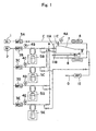
- Fig. 1 is a view schematically showing the whole of a film forming system according to the present example
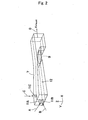
- Fig. 2 is a perspective view schematically showing the construction of a film forming chamber 7 and supply holes
- Fig. 3 is a cross sectional view schematically showing the shape of a film forming chamber 7 and supply holes.
- the system has a bombe 1 for oxygen gas and a bombe 2 for a carrier gas such as argon.
- Oxygen gas is supplied from the bombe 1 for oxygen gas, passed through a mass-flow meter 3A and a valve, and then supplied into a space 12 in the film forming chamber 7 through a third supply hole 11C as an arrow "C".
- a carrier gas is supplied from a bombe 2 for carrier gas, passed through mass-flow meters 3B, 3C, 3D, 3E and valves, and supplied through supply holes 11B and 11C into the film forming chamber 7.
- the carrier gas passed through the mass-flow meters 3B and 3C is mixed with the first metal organic compound supplied from sources 5B and 5C for first metal organic compound to generate a first raw material gas.
- the first raw material gas is supplied through a first supply hole 11A into the film forming chamber 7 as an arrow "A".
- the pressure of the carrier gas is monitored by pressure gauges 4B and 4C.
- the carrier gas passed through the mass-flow meters 3D and 3E is mixed with the second metal organic compound supplied from sources 5D and 5E for second metal organic compound to generate a second raw material gas.
- the second raw material gas is supplied through a second supply hole 11B into the film forming chamber 7 as an arrow "B".
- the pressure of the carrier gas is monitored by pressure gauges 4D and 4E.
- the first raw material gas, second raw material gas and oxygen gas are heated at the corresponding appropriate temperatures direct before they are supplied into the supply holes, respectively.
- the film forming chamber 7 is heated by a heater 6 and the pressure in the chamber 7 is monitored by a pressure gauge 4A.
- a target substrate 9 is set in the chamber 7 and the temperature of the substrate 9 is monitored by a thermocouple 8. Unnecessary gas is evacuated through RP 10 as an arrow "D".
- the supply hole 11C for supplying oxygen gas is provided so that the longitudinal axis of the supply hole 11C is made substantially perpendicular to those of the first supply hole 11A and second supply hole 11B.
- the first supply hole 11A is provided at a position nearer to the third supply hole 11C than the second supply hole 11B.
- Oxygen gas is flown into the chamber 7 as an arrow "C”, and then flown in the space 12 as an arrow "D".
- the first raw material gas is flown into the space 12 through the first supply hole 11A as an arrow "A”, then flown as an arrow "E”, and contacted and mixed with oxygen gas (arrow "D").
- Oxygen gas is further flown while mixed with the first raw material gas, and then mixed with the second raw material gas as an arrow "F”.
- the thus mixed gases are then flown in the space 12 toward the substrate 9, so that a composite oxide is deposited on the substrate 9.
- the decomposition of the first raw material gas is enhanced.
- gas more difficult to decompose having a higher decomposition temperature
- the degree of decomposition of the first raw material gas is made similar to that of the second raw material gas. It is thus possible to improve the surface morphology of the oxide film and the quality of the film.
- the oxide film and structure having the film according to the present invention may be used for applications not particularly limited, including a wavelength converting device, an optical modulating device, a surface acoustic wave device, an optical detection device and a piezoelectric vibrator.
- the wavelength converting device is not limited to a second harmonic generation device, and includes third and fourth harmonic generation devices.
- Such wavelength converting device is particularly suitable for generating a short wavelength light having a wavelength of for example 390 nm to 470 nm.
- the device for generating such a short wavelength light can be preferably applied to various fields such as optical disc memory, medical science, photochemistry, various kinds of light measurements and so on.
- the material for substrate 9 is not particularly limited and may preferably be those already listed for the oxide film. More preferably, the substrate 9 and the oxide film are made of the same kind of material. Alternatively, it is particularly preferred that the material of the substrate 9 is selected from the group consisting of lithium niobate, lithium tantalate, lithium niobate-lithium tantalate solid solution, potassium lithium niobate, potassium lithium tantalate, potassium lithium niobate- potassium lithium tantalate solid solution, potassium niobate and potassium niobate- potassium tantalate solid solution.
- a substrate having a thickness of 0.7 mm and made of a potassium lithium niobate- potassium lithium tantalite solid solution was produced according to micro pull-down process.
- the substrate had a composition of K 3 Li 1.85 (Nb 0.95 Ta 0.05 ) 5.15 O 15 .
- a film of a single crystal of potassium lithium niobate- potassium lithium tantalite solid solution was produced by metal organic vapor deposition according to the above procedure using the system shown in Figs. 1 to 3.
- a reactor made of quartz glass was used.
- the reactor had a double wall structure, for air-tightness, having an outer tube and an inner tube (film forming chamber) 7 for flowing raw material gases, for air tight sealing.
- a table 8 for holding substrate was equipped substantially at the middle flow part in the space 12 of the film forming chamber 7.
- the substrate 9 was mounted on the table 8.
- a thermocouple 8 was mounted at the central part of the substrate 9 to monitor the temperature of the substrate 9.
- the supply holes 11A, 11B and 11C are provided at the upper flow parts of the film forming chamber 7.
- Lithium dipivaloylmethanate Li (C 11 H 19 O 2 )
- potassium dipivaloylmethanate K (C 11 H 19 O 2 )
- Niobium pentaethoxide Nb(OC 2 H 5 ) 5
- a stainless steel container for lithium dipivaloylmethanate was connected in a constant temperature bath 5B
- a stainless steel container for potassium dipivaloylmethanate was connected in a constant temperature bath 5C.
- Stainless steel containers for niobium pentaethoxide were connected in constant temperature baths 5D and 5E.
- the raw material gases were supplied into the film forming chamber 7 under the following conditions.
- Each raw material gas was flown through the corresponding pipe maintained at a temperature higher than the evapolation temperature of the metal organic compound by several tens °C to prevent the deposition of the compound.
- the pipes for ⁇ - diketons lithium dipivaloylmethanate, potassium dipivaloylmethanate
- the pipe for an alkoxide niobium pentaethoxide
- the pipe for oxygen gas was maintained at 250 °C.
- Each raw material gas was introduced into the film forming chamber 7 using argon gas carries while the flow rate of the carrier was controlled.
- the pressure in the film forming chamber 7 was 10 Torr and the temperature of the substrate 9 was 780 °C.
- the time period for the film formation was 4 hours.
- a film of a single crystal of potassium lithium niobate- potassium lithium tantalite solid solution was produced on the substrate 9 of the example 1 by metal organic vapor deposition according to the above procedure using the system shown in Figs. 1 to 3.
- Lithium dipivaloylmethanate Li (C 11 H 19 O 2 )
- magnesium bisacetylacetonate M g (C 5 H 7 O 2 ) 2
- Niobium pentaethoxide Nb(OC 2 H 5 ) 5
- a stainless steel container for lithium dipivaloylmethanate was connected in a constant temperature bath 5B
- a stainless steel container for potassium dipivaloylmethanate was connected in a constant temperature bath 5C.
- Stainless steel containers for niobium pentaethoxide were connected in constant temperature baths 5D and 5E.
- the raw materials gases were supplied into the film forming chamber 7 under the following conditions.
- the pipes for ⁇ - diketons (lithium dipivaloylmethanate, Magnesium bisacetylacetonate) were maintained at about 230 °C, the pipe for an alkoxide (niobium pentaethoxide) was maintained at about 200 °C, and the pipe for oxygen gas was maintained at 250 °C.
- Each raw material gas was introduced into the film forming chamber 7 using argon gas carrier while the flow rate of the carrier was controlled.
- the pressure in the film forming chamber 7 was 10 Torr and the temperature of the substrate 9 was 850 °C.
- the time period for the film formation was 3 hours.
- the pipes for the raw material gases were united outside of the film forming chamber 7 so that the raw material gases were mixed before introducing them into the chamber 7.
- the other conditions were the same as the example 1.
- An oxide film having good surface morphology was not obtained.
- the pipes for the raw material gases were united outside of the film forming chamber so that the raw material gases were mixed before introducing them into the chamber 7.
- the other conditions were the same as the example 2.
- An oxide film having good surface morphology was not obtained.
- an oxide film having good surface morphology and crystal quality can be made, when the film is produced by metal organic chemical vapor deposition using two or more gases of metal organic compounds and oxygen gas.
Landscapes
- Chemical & Material Sciences (AREA)
- Metallurgy (AREA)
- Engineering & Computer Science (AREA)
- Materials Engineering (AREA)
- Organic Chemistry (AREA)
- Crystallography & Structural Chemistry (AREA)
- General Chemical & Material Sciences (AREA)
- Chemical Kinetics & Catalysis (AREA)
- Inorganic Chemistry (AREA)
- Mechanical Engineering (AREA)
- Chemical Vapour Deposition (AREA)
- Crystals, And After-Treatments Of Crystals (AREA)
- Oxygen, Ozone, And Oxides In General (AREA)
Abstract
Description
| Temperature (°C) | Pressure (Torr) | Flow rate (sccm) | |
| Lithium Dipivaloylmethanate Li(DPM) | 188 | 10 | 80 |
| Potassium Dipivaloylmethanate K(DPM) | 187 | 10 | 60 |
| Niobium pentaethoxide Nb(OEt) 5 | 118 | 160 | 250 |
| | Substrate | 9 FWHM of X -ray rocking curve (arc sec) | Oxide film FWHM of X -ray rocking curve (arc sec) |
| 1 | 84 | 74 | |
| 2 | 65 | 59 | |
| 3 | 81 | 53 |
| Temperature (°C) | Container Pressure (Torr) | Flow rate (sccm ) | |
| Lithium Dipivaloylmethanate Li(DPM) | 188 | 10 | 80 |
| Magnesium bisacetylacetonate Mg(Acac)2 | 100 | 10 | 60 |
| Niobium pentaethoxide Nb(OEt)5 | 118 | 160 | 150 |
Claims (8)
- A method of producing an oxide film on a substrate by a metal organic chemical vapor deposition using a film forming system comprising a first supply hole, a second supply hole, a third supply hole and a film forming chamber: said method comprising the step of;
supplying a first raw material gas containing a first metal organic compound through said first supply hole into said chamber, a second raw material gas containing a second metal organic compound through said second supply hole into said chamber, and oxygen gas through said third supply hole into said chamber to form an oxide film, wherein said oxygen gas contacts said first raw material gas before said oxygen gas is mixed with said second raw material gas in said chamber. - The method of claim 1, wherein said first and third supply holes are provided so that a flow of said oxygen gas is crossed at a flow of said first raw material gas in said chamber.
- The method of claim 2, wherein said first and third supply holes are elongated in directions substantially perpendicular to each other.
- The method of any one of claims 1 to 3, wherein said oxide film comprises a crystal having an electro-optic effect.
- The method of claim 4, wherein said oxide is selected from the group consisting of lithium niobate, lithium tantalate, lithium niobate-lithium tantalate solid solution, potassium lithium niobate, potassium lithium tantalate and potassium lithium niobate- potassium lithium tantalate solid solution.
- The method of any one of claims 1 to 5, wherein said first metal organic compound comprises a β-diketone compound and said second metal organic compound comprises an alkoxide.
- An oxide film obtained by the method of any on of claims 1 to 6.
- A film structure comprising a substrate and the oxide film of claim 7.
Applications Claiming Priority (3)
| Application Number | Priority Date | Filing Date | Title |
|---|---|---|---|
| JP2003063418A JP4251537B2 (en) | 2003-03-10 | 2003-03-10 | Method for producing oxide coating |
| JP2003063418 | 2003-03-10 | ||
| PCT/JP2004/002964 WO2004081265A1 (en) | 2003-03-10 | 2004-03-08 | Method for forming oxide coating film, oxide coating film and coating film structure |
Publications (3)
| Publication Number | Publication Date |
|---|---|
| EP1607498A1 true EP1607498A1 (en) | 2005-12-21 |
| EP1607498A4 EP1607498A4 (en) | 2009-05-27 |
| EP1607498B1 EP1607498B1 (en) | 2012-08-22 |
Family
ID=32984429
Family Applications (1)
| Application Number | Title | Priority Date | Filing Date |
|---|---|---|---|
| EP04718392A Expired - Lifetime EP1607498B1 (en) | 2003-03-10 | 2004-03-08 | Method for forming oxide coating film, oxide coating film and coating film structure |
Country Status (5)
| Country | Link |
|---|---|
| US (1) | US7517557B2 (en) |
| EP (1) | EP1607498B1 (en) |
| JP (1) | JP4251537B2 (en) |
| KR (1) | KR100845483B1 (en) |
| WO (1) | WO2004081265A1 (en) |
Families Citing this family (2)
| Publication number | Priority date | Publication date | Assignee | Title |
|---|---|---|---|---|
| JP6022228B2 (en) | 2011-09-14 | 2016-11-09 | 株式会社日立国際電気 | Semiconductor device manufacturing method, substrate processing method, substrate processing apparatus, and program |
| CN104264129B (en) * | 2014-10-20 | 2016-09-28 | 佛山市中山大学研究院 | The air intake installation of a kind of MOCVD device and MOCVD device |
Family Cites Families (13)
| Publication number | Priority date | Publication date | Assignee | Title |
|---|---|---|---|---|
| US4699675A (en) * | 1985-12-26 | 1987-10-13 | Rca Corporation | Vapor phase growth of III-V materials |
| EP0252755A1 (en) * | 1986-07-11 | 1988-01-13 | Unvala Limited | Chemical vapour deposition |
| JP2502397B2 (en) | 1990-03-01 | 1996-05-29 | シャープ株式会社 | Signal generation circuit |
| JPH0375207A (en) | 1989-08-15 | 1991-03-29 | Furukawa Electric Co Ltd:The | Production of thin film of oxide superconductor |
| US5280012A (en) * | 1990-07-06 | 1994-01-18 | Advanced Technology Materials Inc. | Method of forming a superconducting oxide layer by MOCVD |
| JP3253295B2 (en) | 1990-09-07 | 2002-02-04 | 株式会社東芝 | Manufacturing method of oxide thin film |
| JP3328389B2 (en) | 1993-09-14 | 2002-09-24 | 康夫 垂井 | Manufacturing method of ferroelectric thin film |
| US5527567A (en) | 1994-09-02 | 1996-06-18 | Ceram Incorporated | Metalorganic chemical vapor deposition of layered structure oxides |
| US5753300A (en) * | 1995-06-19 | 1998-05-19 | Northwestern University | Oriented niobate ferroelectric thin films for electrical and optical devices and method of making such films |
| JP3809669B2 (en) | 1996-07-30 | 2006-08-16 | 日産自動車株式会社 | Chemical vapor deposition |
| JP3208377B2 (en) * | 1997-08-22 | 2001-09-10 | ポリプラスチックス株式会社 | Continuous production method of polyacetal resin |
| US6513226B2 (en) * | 2000-03-28 | 2003-02-04 | Ngk Insulators, Ltd. | Method of manufacturing film structure, method of manufacturing optical waveguide substrate and method of manufacturing second harmonic generation device |
| JP2001343544A (en) | 2000-03-28 | 2001-12-14 | Ngk Insulators Ltd | Method for producing film structural body, method for producing optical guide substrate and method for producing second harmonic generation element |
-
2003
- 2003-03-10 JP JP2003063418A patent/JP4251537B2/en not_active Expired - Fee Related
-
2004
- 2004-03-05 US US10/792,852 patent/US7517557B2/en not_active Expired - Fee Related
- 2004-03-08 KR KR1020057016822A patent/KR100845483B1/en not_active Expired - Fee Related
- 2004-03-08 WO PCT/JP2004/002964 patent/WO2004081265A1/en not_active Ceased
- 2004-03-08 EP EP04718392A patent/EP1607498B1/en not_active Expired - Lifetime
Also Published As
| Publication number | Publication date |
|---|---|
| KR20050109075A (en) | 2005-11-17 |
| KR100845483B1 (en) | 2008-07-10 |
| US20090074963A1 (en) | 2009-03-19 |
| US7517557B2 (en) | 2009-04-14 |
| EP1607498B1 (en) | 2012-08-22 |
| JP4251537B2 (en) | 2009-04-08 |
| WO2004081265A1 (en) | 2004-09-23 |
| JP2004269320A (en) | 2004-09-30 |
| EP1607498A4 (en) | 2009-05-27 |
Similar Documents
| Publication | Publication Date | Title |
|---|---|---|
| JP3462265B2 (en) | Wavelength conversion element | |
| US6632725B2 (en) | Process for producing an epitaxial layer of gallium nitride by the HVPE method | |
| Feigelson | Epitaxial growth of lithium niobate thin films by the solid source MOCVD method | |
| WO2003085711A1 (en) | VAPOR PHASE GROWTH METHOD FOR Al-CONTAINING III-V GROUP COMPOUND SEMICONDUCTOR, AND METHOD AND DEVICE FOR PRODUCING Al-CONTAINING III-V GROUP COMPOUND SEMICONDUCTOR | |
| EP0111510B1 (en) | Low temperature process for depositing epitaxial layers | |
| JPH02255595A (en) | Method and device for vaporizing and supplying organometallic compound | |
| US7517557B2 (en) | Oxide films, a method of producing the same and structures having the same | |
| JP3665682B2 (en) | Method for producing fluoride thin film | |
| JP2002080296A (en) | Quartz thin film and method of manufacturing the same | |
| EP0617141A1 (en) | Improved method for growing continuous diamond films | |
| Chikuma et al. | Waveguiding Epitaxial Potassium Lithium Niobate Single-Crystal Films Deposited by Metalorganic Chemical Vapor Deposition | |
| Onoe et al. | Epitaxial growth of orientation-controlled KNbO 3 crystal films on MgO using KTa x Nb 1− x O 3 intermediate layer by metalorganic chemical vapor deposition | |
| JP3932017B2 (en) | Method for producing iron silicide crystal | |
| Shin et al. | Preparation of lithium niobate thin film by thermal chemical vapor deposition | |
| US6513226B2 (en) | Method of manufacturing film structure, method of manufacturing optical waveguide substrate and method of manufacturing second harmonic generation device | |
| Iwai et al. | Epitaxial growth of MgO-doped lithium niobate thin films by metalorganic chemical vapor deposition | |
| JP2001343544A (en) | Method for producing film structural body, method for producing optical guide substrate and method for producing second harmonic generation element | |
| JPS6135847A (en) | Method of manufacturing thin film | |
| Graettinger et al. | Growth of epitaxial KNbO3 thin films | |
| Fazlioglu Yalcin | Elucidating the Growth Kinetics of Hybrid Molecular Beam Epitaxy: An Experimental and Computational Approach | |
| JPH04301329A (en) | Manufacture of ferroelectric thin film | |
| JP3183939B2 (en) | Method for producing zinc oxide single crystal thin film | |
| JPH0340920A (en) | Production of thin zirconia film | |
| JPH11326967A (en) | Second harmonic generation element | |
| JP4275615B2 (en) | Dielectric element |
Legal Events
| Date | Code | Title | Description |
|---|---|---|---|
| PUAI | Public reference made under article 153(3) epc to a published international application that has entered the european phase |
Free format text: ORIGINAL CODE: 0009012 |
|
| 17P | Request for examination filed |
Effective date: 20050922 |
|
| AK | Designated contracting states |
Kind code of ref document: A1 Designated state(s): AT BE BG CH CY CZ DE DK EE ES FI FR GB GR HU IE IT LI LU MC NL PL PT RO SE SI SK TR |
|
| AX | Request for extension of the european patent |
Extension state: AL LT LV MK |
|
| DAX | Request for extension of the european patent (deleted) | ||
| RBV | Designated contracting states (corrected) |
Designated state(s): DE FR |
|
| A4 | Supplementary search report drawn up and despatched |
Effective date: 20090427 |
|
| RIC1 | Information provided on ipc code assigned before grant |
Ipc: C30B 25/02 20060101ALI20090421BHEP Ipc: C23C 16/40 20060101ALI20090421BHEP Ipc: C23C 16/455 20060101ALI20090421BHEP Ipc: C30B 29/30 20060101ALI20090421BHEP Ipc: C30B 25/14 20060101AFI20040927BHEP |
|
| 17Q | First examination report despatched |
Effective date: 20100115 |
|
| GRAP | Despatch of communication of intention to grant a patent |
Free format text: ORIGINAL CODE: EPIDOSNIGR1 |
|
| GRAS | Grant fee paid |
Free format text: ORIGINAL CODE: EPIDOSNIGR3 |
|
| GRAA | (expected) grant |
Free format text: ORIGINAL CODE: 0009210 |
|
| AK | Designated contracting states |
Kind code of ref document: B1 Designated state(s): DE FR |
|
| REG | Reference to a national code |
Ref country code: DE Ref legal event code: R096 Ref document number: 602004039020 Country of ref document: DE Effective date: 20121018 |
|
| PLBE | No opposition filed within time limit |
Free format text: ORIGINAL CODE: 0009261 |
|
| STAA | Information on the status of an ep patent application or granted ep patent |
Free format text: STATUS: NO OPPOSITION FILED WITHIN TIME LIMIT |
|
| 26N | No opposition filed |
Effective date: 20130523 |
|
| REG | Reference to a national code |
Ref country code: DE Ref legal event code: R097 Ref document number: 602004039020 Country of ref document: DE Effective date: 20130523 |
|
| PGFP | Annual fee paid to national office [announced via postgrant information from national office to epo] |
Ref country code: FR Payment date: 20140311 Year of fee payment: 11 |
|
| PGFP | Annual fee paid to national office [announced via postgrant information from national office to epo] |
Ref country code: DE Payment date: 20140417 Year of fee payment: 11 |
|
| REG | Reference to a national code |
Ref country code: DE Ref legal event code: R119 Ref document number: 602004039020 Country of ref document: DE |
|
| REG | Reference to a national code |
Ref country code: FR Ref legal event code: ST Effective date: 20151130 |
|
| PG25 | Lapsed in a contracting state [announced via postgrant information from national office to epo] |
Ref country code: DE Free format text: LAPSE BECAUSE OF NON-PAYMENT OF DUE FEES Effective date: 20151001 |
|
| PG25 | Lapsed in a contracting state [announced via postgrant information from national office to epo] |
Ref country code: FR Free format text: LAPSE BECAUSE OF NON-PAYMENT OF DUE FEES Effective date: 20150331 |