EP1606144B1 - Power fold mirror control circuit and method - Google Patents
Power fold mirror control circuit and method Download PDFInfo
- Publication number
- EP1606144B1 EP1606144B1 EP04723135A EP04723135A EP1606144B1 EP 1606144 B1 EP1606144 B1 EP 1606144B1 EP 04723135 A EP04723135 A EP 04723135A EP 04723135 A EP04723135 A EP 04723135A EP 1606144 B1 EP1606144 B1 EP 1606144B1
- Authority
- EP
- European Patent Office
- Prior art keywords
- control circuit
- vehicle mirror
- fold
- mirror
- transistor
- Prior art date
- Legal status (The legal status is an assumption and is not a legal conclusion. Google has not performed a legal analysis and makes no representation as to the accuracy of the status listed.)
- Expired - Lifetime
Links
Images
Classifications
-
- B—PERFORMING OPERATIONS; TRANSPORTING
- B60—VEHICLES IN GENERAL
- B60R—VEHICLES, VEHICLE FITTINGS, OR VEHICLE PARTS, NOT OTHERWISE PROVIDED FOR
- B60R1/00—Optical viewing arrangements; Real-time viewing arrangements for drivers or passengers using optical image capturing systems, e.g. cameras or video systems specially adapted for use in or on vehicles
- B60R1/02—Rear-view mirror arrangements
- B60R1/06—Rear-view mirror arrangements mounted on vehicle exterior
- B60R1/062—Rear-view mirror arrangements mounted on vehicle exterior with remote control for adjusting position
-
- H—ELECTRICITY
- H02—GENERATION; CONVERSION OR DISTRIBUTION OF ELECTRIC POWER
- H02H—EMERGENCY PROTECTIVE CIRCUIT ARRANGEMENTS
- H02H5/00—Emergency protective circuit arrangements for automatic disconnection directly responsive to an undesired change from normal non-electric working conditions with or without subsequent reconnection
- H02H5/04—Emergency protective circuit arrangements for automatic disconnection directly responsive to an undesired change from normal non-electric working conditions with or without subsequent reconnection responsive to abnormal temperature
- H02H5/042—Emergency protective circuit arrangements for automatic disconnection directly responsive to an undesired change from normal non-electric working conditions with or without subsequent reconnection responsive to abnormal temperature using temperature dependent resistors
-
- B—PERFORMING OPERATIONS; TRANSPORTING
- B60—VEHICLES IN GENERAL
- B60R—VEHICLES, VEHICLE FITTINGS, OR VEHICLE PARTS, NOT OTHERWISE PROVIDED FOR
- B60R1/00—Optical viewing arrangements; Real-time viewing arrangements for drivers or passengers using optical image capturing systems, e.g. cameras or video systems specially adapted for use in or on vehicles
- B60R1/02—Rear-view mirror arrangements
- B60R1/06—Rear-view mirror arrangements mounted on vehicle exterior
- B60R1/062—Rear-view mirror arrangements mounted on vehicle exterior with remote control for adjusting position
- B60R1/07—Rear-view mirror arrangements mounted on vehicle exterior with remote control for adjusting position by electrically powered actuators
-
- B—PERFORMING OPERATIONS; TRANSPORTING
- B60—VEHICLES IN GENERAL
- B60R—VEHICLES, VEHICLE FITTINGS, OR VEHICLE PARTS, NOT OTHERWISE PROVIDED FOR
- B60R1/00—Optical viewing arrangements; Real-time viewing arrangements for drivers or passengers using optical image capturing systems, e.g. cameras or video systems specially adapted for use in or on vehicles
- B60R1/02—Rear-view mirror arrangements
- B60R1/06—Rear-view mirror arrangements mounted on vehicle exterior
- B60R1/062—Rear-view mirror arrangements mounted on vehicle exterior with remote control for adjusting position
- B60R1/07—Rear-view mirror arrangements mounted on vehicle exterior with remote control for adjusting position by electrically powered actuators
- B60R1/074—Rear-view mirror arrangements mounted on vehicle exterior with remote control for adjusting position by electrically powered actuators for retracting the mirror arrangements to a non-use position alongside the vehicle
-
- B—PERFORMING OPERATIONS; TRANSPORTING
- B60—VEHICLES IN GENERAL
- B60R—VEHICLES, VEHICLE FITTINGS, OR VEHICLE PARTS, NOT OTHERWISE PROVIDED FOR
- B60R16/00—Electric or fluid circuits specially adapted for vehicles and not otherwise provided for; Arrangement of elements of electric or fluid circuits specially adapted for vehicles and not otherwise provided for
- B60R16/02—Electric or fluid circuits specially adapted for vehicles and not otherwise provided for; Arrangement of elements of electric or fluid circuits specially adapted for vehicles and not otherwise provided for electric constitutive elements
- B60R16/023—Electric or fluid circuits specially adapted for vehicles and not otherwise provided for; Arrangement of elements of electric or fluid circuits specially adapted for vehicles and not otherwise provided for electric constitutive elements for transmission of signals between vehicle parts or subsystems
- B60R16/0231—Circuits relating to the driving or the functioning of the vehicle
-
- G—PHYSICS
- G01—MEASURING; TESTING
- G01K—MEASURING TEMPERATURE; MEASURING QUANTITY OF HEAT; THERMALLY-SENSITIVE ELEMENTS NOT OTHERWISE PROVIDED FOR
- G01K13/00—Thermometers specially adapted for specific purposes
-
- H—ELECTRICITY
- H01—ELECTRIC ELEMENTS
- H01H—ELECTRIC SWITCHES; RELAYS; SELECTORS; EMERGENCY PROTECTIVE DEVICES
- H01H43/00—Time or time-programme switches providing a choice of time-intervals for executing one or more switching actions and automatically terminating their operation after the programme is completed
- H01H43/30—Time or time-programme switches providing a choice of time-intervals for executing one or more switching actions and automatically terminating their operation after the programme is completed with timing of actuation of contacts due to thermal action
- H01H43/308—Time or time-programme switches providing a choice of time-intervals for executing one or more switching actions and automatically terminating their operation after the programme is completed with timing of actuation of contacts due to thermal action based on the change of electrical properties, e.g. thermistors
-
- H—ELECTRICITY
- H02—GENERATION; CONVERSION OR DISTRIBUTION OF ELECTRIC POWER
- H02H—EMERGENCY PROTECTIVE CIRCUIT ARRANGEMENTS
- H02H7/00—Emergency protective circuit arrangements specially adapted for specific types of electric machines or apparatus or for sectionalised protection of cable or line systems, and effecting automatic switching in the event of an undesired change from normal working conditions
- H02H7/08—Emergency protective circuit arrangements specially adapted for specific types of electric machines or apparatus or for sectionalised protection of cable or line systems, and effecting automatic switching in the event of an undesired change from normal working conditions for dynamo-electric motors
- H02H7/0816—Emergency protective circuit arrangements specially adapted for specific types of electric machines or apparatus or for sectionalised protection of cable or line systems, and effecting automatic switching in the event of an undesired change from normal working conditions for dynamo-electric motors concerning the starting sequence, e.g. limiting the number of starts per time unit, monitoring speed during starting
Definitions
- This invention relates to the control of power fold mirrors on vehicles.
- the driver is able to manually control the position of the mirror such that, when, for example the car is parked, the driver will switch the mirror into a folded position to lie adjacent to the external surface of the car.
- the driver can select the fold out position and the mirror will fold out from the side of the car and assume an extended position in the normal fashion, to allow the mirror to be used while driving.
- small electric motors drive the movement of the mirror and in doing so, generate heat.
- the power fold function is used infrequently, the generation of heat is not a major problem.
- the power fold function is used frivolously, for example a child playing with the power fold switch and repeatedly folding the mirror in and out. This may result in overheating of the motor and surrounding electronic components and may damage the components of the mirror system.
- a mirror resp. a method according to preamble of claim 1 resp. 5 is known from US 5,627,710 .
- a control circuit for controlling the operation of a motor of a power fold vehicle mirror including:
- a method of controlling the operation of a motor of a power fold vehicle mirror, controlled by a control circuit including preventing the vehicle mirror from at least folding in if a temperature of at least a portion of the control circuit reaches or exceeds a predetermined temperature threshold.
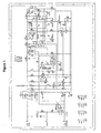
- Figure 1 shows a circuit diagram of a control circuit for controlling the operation of a power fold mirror.
- the vehicle interface has two supply leads (A and B) and a door signal line (D).
- door signal line D When door signal line D is open circuit, the motor polarity is determined by the supply polarity.
- Door signal D equates to the state of the vehicle door.
- a and B are provided by the state of a "fold in/fold out" control switch, operated by a user.
- Door signal line D input is supplied with a positive bias current from R19 via D6 from whichever of A or B is positive. From Table 1, it can be seen that the function is always "fold out” unless A is positive, D is open and B is negative. In order to select "fold in", digital transistors Q13 must be biased on. This occurs only when Q12 is biased on which can only occur if B is negative and D is open. In this case, a current flows from D6 to R19 to R21, to bias Q12B on and draw current through R22 which biases digital transistors Q13 on. If D is negative, then Q12B cannot be biased on and if B is positive, Q12B cannot draw current through R22 to bias Q13 on. Thus, Q13 is biased on only when the "fold in” function is required.
- the mirror should not be able to fold in if the vehicle door is open, as this will interfere with the operation of the mirror.
- Transistor Q12A is used to protect the junction of Q12B from excessive reverse bias voltage.
- Capacitor C7 provides immunity from high frequency interference and R20 provides immunity from RF and small leakage currents on the D input line.
- Capacitor C8 is provided to prevent changes to the input states that only last a short time from changing the function of the device.
- Diodes D2 to D5 form a conventional full wave rectifier circuit.
- Capacitor C2 is used to bias the circuit during supply interruptions, reducing interfering signals from the motor being transmitted to the vehicle interface leads and improve the input impulse transient immunity. While the vehicle interface is energised, the cathode of diode D2 is positive and anode of diode D3 is negative, regardless of the polarity of the incoming supply signal.
- Capacitors C3 and C4 connect the input to the output of the rectifying circuits or bridge, for high frequencies even when none of the diodes is positively biased. This reduces EMC emissions and susceptibility.
- Transistors Q10 and Q7 form a conventional H bridge allowing polarity control.
- transistor Q13 When transistor Q13 is on, transistor Q7A is on making the motor input terminal MA negative.
- Q13 being on, also biases Q10A off and Q14 off (via Q9 and R23).
- Transistor Q14 is biased off, allowing R16 to bias Q10B on and Q7B off, making motor terminal MB positive.
- Q13 is off, all of the above states are reversed and motor terminal MA is positive and motor terminal MB is negative.
- Capacitor C9 reduces the interference produced by the motor passing through the circuit to the vehicle interface. Diode D7 prevents transients on the supply from damaging transistors Q7A and Q10A via R15.
- Diode D1 biased by R2, provides a voltage reference, which may be shunted off by either of the SCR-configured transistor pairs Q11A with Q11B and Q8A with Q8B (the function of which will be discussed further below).
- Transistor Q3 and resistor R9 buffer the voltage regulator output.
- Transistors Q2A with Q2B form a voltage comparator of the "long tail pair" variety, biased by R3.
- the current provided by R3 is steered in varying proportions between the collector of transistor Q2B to supply return or to the collector of transistor Q2A, generating a voltage on R4.
- the input of the comparator is fed with the voltage reference on one side and with a percentage of the voltage supplied to the output polarity control circuit (incorporating transistors Q10 and Q7 as described above) by the ratiometric potential divider made up by resistors R7, R10 and R6.
- the output of the comparator (being the voltage developed across resistor R4) controls the bias of transistor Q6, which forms the voltage regulator pass element.
- Capacitor C1 and resistor R30 control the gain roll-off and phase of the loop to prevent oscillation of the circuit.
- the voltage of the output polarity control circuit and hence the output to the motor is thus voltage regulated to a multiple of the referenced voltage.
- the current through the output terminals, the output polarity control circuit and the voltage regulator flows through current sense resistors R17 and R18, generating a voltage feeding resistor R14, proportional to the current.
- This voltage is summed with the voltage produced by a current from R1 acting on R14.
- This current is introduced to modify the voltage produced by the current according to the temperature of the circuit.
- Applying the reference voltage as described above to the series combination of resistors R5 and R8 creates the current.
- Resistor R8 has a high and non-linear defined negative temperature coefficient of resistance to temperature (otherwise known as a thermistor). The current this produces increases with temperature. Given that the base current of transistor Q1A is small, the emitter current and collector current are approximately equal. This additional current flows into resistor R14 via resistor R1. Once the current in R1 is sufficient to produce a voltage across it such that Q1B starts to bias on, then any additional current flows in the negative supply and not through R14.
- transistor Q5B draws current away from the gate of transistor Q6 to control the current
- transistor Q5A is turned on and diode D8 is biased via resistors R13 and R26 to provide a voltage of approximately 1.2 volts below the positive supply rail. This charges capacitor C5 and C6 through resistors R25 and R24 respectively.
- transistor Q13 In the “fold in” function, transistor Q13 is biased on and as such, capacitor C6 is prevented from charging but capacitor C5 can charge. In the “fold out” function, the reverse is true and transistor Q14 is on which prevents capacitor C5 from charging but allows capacitor C6 to charge.
- transistor Q8A When capacitor C5 charges enough, transistor Q8A will start to bias on, which will bias transistor Q8B on, which will further bias transistor Q8A on. The effect is that transistors Q8A and B snap on (as in an SCR). When this happens, the voltage reference across diode D1 is shunted and the regulated voltage falls close to zero causing the motor to be off. This state only ends when transistor Q14 is biased on to unlatch the arrangement, which happens when the function changes from "fold in” to "fold out”. Resistor R27 prevents leakage currents causing false activation of the circuit.
- transistor Q11A When capacitor C6 charges enough, transistor Q11A will start to bias on which will bias Q11B on, which will further bias transistor Q11A on. The effect is that Q11A and B snap on (again, as in an SCR). When this happens, the motor is off. This state only ends when transistor Q13 is biased on to unlatch the arrangement, which happens when the function changes from "fold out” to "fold in”. Resistor R28 prevents leakage currents causing false activation of the circuit.
- the portion of the circuit which controls the function of the mirror in accordance with the invention includes resistors R13 and R12 which form a potential divider from the referenced voltage.
- Resistor R13 has a high and non-linear defined negative temperature coefficient of resistance to temperature as does resistor R8 as previously described. As the temperature increases, the voltage feeding resistor R11 increases (provided that the reference voltage is not shunted).
- transistor Q4B When this voltage is high enough to start biasing resistor Q4A on, transistor Q4B is biased on which in turn biases Q4A harder on. The result is that the circuit latches on, pulling transistor Q13 off. As previously described, when transistor Q13 is off, the control circuit assumes the "fold out” function and cannot fold the mirror in.
- Resistor R29 prevents leakage current from falsely activating the circuit. Accordingly, if the unit were asked to operate (with voltage reference being unshunted) but at too high a temperature, the control circuit will be forced to an "fold out” state and will remain in that "fold out” state until the temperature reduces.
- resistor R13 and associated components will be chosen such as to cause transistor Q13 to turn off, and hence assume the "fold out” position, when the temperature of resistor R13 reaches a preset threshold. Accordingly, once the temperature of the circuit, and more particularly resistor R13, reaches an undesirable level, the control circuit will prevent the mirror from folding in, until the temperature has dropped to a safer level, at which time transistor Q13 will be allowed to turn on, and the control circuit will be allowed to assume the "fold in” state.
- the sense resistor R13 is placed adjacent to the components most needing temperature protection, typically the output transistors Q7 and Q10.
- the mirror Because when transistor Q13 is on, and the circuit is in the "fold in” state, the mirror is still able to be operated, but only to cause it to be folded out. In this way, even though the temperature of the circuit and surrounding components may be too high, the mirror may still be folded out to allow the door to be opened, and the car to be driven, however, the mirror will not be allowed to be folded in until the temperature has reduced to safer levels.
Landscapes
- Engineering & Computer Science (AREA)
- Mechanical Engineering (AREA)
- Multimedia (AREA)
- Physics & Mathematics (AREA)
- General Physics & Mathematics (AREA)
- Automation & Control Theory (AREA)
- Rear-View Mirror Devices That Are Mounted On The Exterior Of The Vehicle (AREA)
- Folding Of Thin Sheet-Like Materials, Special Discharging Devices, And Others (AREA)
- Illuminated Signs And Luminous Advertising (AREA)
- Transmitters (AREA)
Abstract
Description
- This invention relates to the control of power fold mirrors on vehicles.
- A standard feature of many modern vehicles, including private and industrial vehicles, is the ability for one or more side mirrors of the vehicle to fold in and out from the side of the vehicle. The driver is able to manually control the position of the mirror such that, when, for example the car is parked, the driver will switch the mirror into a folded position to lie adjacent to the external surface of the car. When the car is about to be driven, the driver can select the fold out position and the mirror will fold out from the side of the car and assume an extended position in the normal fashion, to allow the mirror to be used while driving.
- A common factor to be taken into consideration when designing electronic circuits, particularly when associated with mechanical actuators, is the production of heat. In the case of fold out mirrors, small electric motors drive the movement of the mirror and in doing so, generate heat. Traditionally, because the power fold function is used infrequently, the generation of heat is not a major problem. However, there may be instances where the power fold function is used frivolously, for example a child playing with the power fold switch and repeatedly folding the mirror in and out. This may result in overheating of the motor and surrounding electronic components and may damage the components of the mirror system.
- Traditional ways of dealing with overheating include the provision of heat sinks, which provide a large surface area in contact with the surrounding air to radiate heat therefrom, and in the case of circuit boards, larger PCBs can be used to provide the larger heat radiating area.
- Other methods of compensating for the generation of heat include using heavier duty components which are more expensive. This is undesirable in a product which is mass manufactured as the overall increase in cost can be dramatic. Similarly, in devices such as power fold control circuits, space is often at a premium and it is necessary to keep component and board sizes as small as possible.
- It is an object of the present invention to provide an alternative means of addressing the problem of potentially damaging heat.
- A mirror resp. a method according to preamble of claim 1 resp. 5 is known from
US 5,627,710 . - According to a first aspect of the present invention, there is provided a control circuit for controlling the operation of a motor of a power fold vehicle mirror, the control circuit including:
- a temperature sensor; and
- a vehicle mirror actuation control; wherein
- upon the temperature sensor sensing that a temperature of at least a portion of the control circuit has reached or exceeded a predetermined temperature threshold, the vehicle mirror actuation control prevents the vehicle mirror from at least folding in.
- According to a second aspect of the present invention, there is provided a method of controlling the operation of a motor of a power fold vehicle mirror, controlled by a control circuit, the method including preventing the vehicle mirror from at least folding in if a temperature of at least a portion of the control circuit reaches or exceeds a predetermined temperature threshold.
- A preferred embodiment of the present invention will now be described with reference to the following Figures in which:
- Figure 1 is a circuit diagram including a control circuit according to the present invention.
- Figure 1 shows a circuit diagram of a control circuit for controlling the operation of a power fold mirror.
- The vehicle interface has two supply leads (A and B) and a door signal line (D). When door signal line D is open circuit, the motor polarity is determined by the supply polarity. Door signal D equates to the state of the vehicle door. A and B are provided by the state of a "fold in/fold out" control switch, operated by a user.
- When door signal line D is connected to the negative supply lead, then the polarity of A and B have no effect on the motor polarity. The motor polarity is shown in Table 1 below, where A, D and B are the inputs described above and MA and MB are the terminals of the motor. The "function" column indicates the function of the mirror resulting from the combination of the signals on inputs A, D and B.
Table 1 Input Output A D B MA MB Function + Open - - + Fold In - Open + + - Fold Out - - + + - Fold Out + - - + - Fold Out - Door signal line D input is supplied with a positive bias current from R19 via D6 from whichever of A or B is positive. From Table 1, it can be seen that the function is always "fold out" unless A is positive, D is open and B is negative. In order to select "fold in", digital transistors Q13 must be biased on. This occurs only when Q12 is biased on which can only occur if B is negative and D is open. In this case, a current flows from D6 to R19 to R21, to bias Q12B on and draw current through R22 which biases digital transistors Q13 on. If D is negative, then Q12B cannot be biased on and if B is positive, Q12B cannot draw current through R22 to bias Q13 on. Thus, Q13 is biased on only when the "fold in" function is required.
- It will be appreciated that the mirror should not be able to fold in if the vehicle door is open, as this will interfere with the operation of the mirror.
- Transistor Q12A is used to protect the junction of Q12B from excessive reverse bias voltage. Capacitor C7 provides immunity from high frequency interference and R20 provides immunity from RF and small leakage currents on the D input line. Capacitor C8 is provided to prevent changes to the input states that only last a short time from changing the function of the device. Diodes D2 to D5 form a conventional full wave rectifier circuit. Capacitor C2 is used to bias the circuit during supply interruptions, reducing interfering signals from the motor being transmitted to the vehicle interface leads and improve the input impulse transient immunity. While the vehicle interface is energised, the cathode of diode D2 is positive and anode of diode D3 is negative, regardless of the polarity of the incoming supply signal.
- Capacitors C3 and C4 connect the input to the output of the rectifying circuits or bridge, for high frequencies even when none of the diodes is positively biased. This reduces EMC emissions and susceptibility.
- Transistors Q10 and Q7 form a conventional H bridge allowing polarity control. When transistor Q13 is on, transistor Q7A is on making the motor input terminal MA negative. Q13, being on, also biases Q10A off and Q14 off (via Q9 and R23). Transistor Q14 is biased off, allowing R16 to bias Q10B on and Q7B off, making motor terminal MB positive. When Q13 is off, all of the above states are reversed and motor terminal MA is positive and motor terminal MB is negative.
- Capacitor C9 reduces the interference produced by the motor passing through the circuit to the vehicle interface. Diode D7 prevents transients on the supply from damaging transistors Q7A and Q10A via R15.
- Diode D1, biased by R2, provides a voltage reference, which may be shunted off by either of the SCR-configured transistor pairs Q11A with Q11B and Q8A with Q8B (the function of which will be discussed further below). Transistor Q3 and resistor R9 buffer the voltage regulator output.
- Transistors Q2A with Q2B form a voltage comparator of the "long tail pair" variety, biased by R3. The current provided by R3 is steered in varying proportions between the collector of transistor Q2B to supply return or to the collector of transistor Q2A, generating a voltage on R4.
- The input of the comparator is fed with the voltage reference on one side and with a percentage of the voltage supplied to the output polarity control circuit (incorporating transistors Q10 and Q7 as described above) by the ratiometric potential divider made up by resistors R7, R10 and R6.
- The output of the comparator (being the voltage developed across resistor R4) controls the bias of transistor Q6, which forms the voltage regulator pass element.
- Capacitor C1 and resistor R30 control the gain roll-off and phase of the loop to prevent oscillation of the circuit.
- The voltage of the output polarity control circuit and hence the output to the motor is thus voltage regulated to a multiple of the referenced voltage.
- The current through the output terminals, the output polarity control circuit and the voltage regulator, flows through current sense resistors R17 and R18, generating a voltage feeding resistor R14, proportional to the current. This voltage is summed with the voltage produced by a current from R1 acting on R14. This current is introduced to modify the voltage produced by the current according to the temperature of the circuit. Applying the reference voltage as described above to the series combination of resistors R5 and R8 creates the current. Resistor R8 has a high and non-linear defined negative temperature coefficient of resistance to temperature (otherwise known as a thermistor). The current this produces increases with temperature. Given that the base current of transistor Q1A is small, the emitter current and collector current are approximately equal. This additional current flows into resistor R14 via resistor R1. Once the current in R1 is sufficient to produce a voltage across it such that Q1B starts to bias on, then any additional current flows in the negative supply and not through R14.
- Once the summing of R14 is such that the transistor Q5B starts to be biased, drive from transistor Q6 is pulled away via the base-emitter junction of transistor Q5A. In this way, the current is limited through transistor Q6 and hence the motor current is limited.
- When transistor Q5B draws current away from the gate of transistor Q6 to control the current, transistor Q5A is turned on and diode D8 is biased via resistors R13 and R26 to provide a voltage of approximately 1.2 volts below the positive supply rail. This charges capacitor C5 and C6 through resistors R25 and R24 respectively.
- In the "fold in" function, transistor Q13 is biased on and as such, capacitor C6 is prevented from charging but capacitor C5 can charge. In the "fold out" function, the reverse is true and transistor Q14 is on which prevents capacitor C5 from charging but allows capacitor C6 to charge.
- When capacitor C5 charges enough, transistor Q8A will start to bias on, which will bias transistor Q8B on, which will further bias transistor Q8A on. The effect is that transistors Q8A and B snap on (as in an SCR). When this happens, the voltage reference across diode D1 is shunted and the regulated voltage falls close to zero causing the motor to be off. This state only ends when transistor Q14 is biased on to unlatch the arrangement, which happens when the function changes from "fold in" to "fold out". Resistor R27 prevents leakage currents causing false activation of the circuit.
- When capacitor C6 charges enough, transistor Q11A will start to bias on which will bias Q11B on, which will further bias transistor Q11A on. The effect is that Q11A and B snap on (again, as in an SCR). When this happens, the motor is off. This state only ends when transistor Q13 is biased on to unlatch the arrangement, which happens when the function changes from "fold out" to "fold in". Resistor R28 prevents leakage currents causing false activation of the circuit.
- The portion of the circuit which controls the function of the mirror in accordance with the invention includes resistors R13 and R12 which form a potential divider from the referenced voltage. Resistor R13 has a high and non-linear defined negative temperature coefficient of resistance to temperature as does resistor R8 as previously described. As the temperature increases, the voltage feeding resistor R11 increases (provided that the reference voltage is not shunted).
- When this voltage is high enough to start biasing resistor Q4A on, transistor Q4B is biased on which in turn biases Q4A harder on. The result is that the circuit latches on, pulling transistor Q13 off. As previously described, when transistor Q13 is off, the control circuit assumes the "fold out" function and cannot fold the mirror in.
- Resistor R29 prevents leakage current from falsely activating the circuit.
Accordingly, if the unit were asked to operate (with voltage reference being unshunted) but at too high a temperature, the control circuit will be forced to an "fold out" state and will remain in that "fold out" state until the temperature reduces. - As will be obvious to the person skilled in the art, the value of resistor R13 and associated components will be chosen such as to cause transistor Q13 to turn off, and hence assume the "fold out" position, when the temperature of resistor R13 reaches a preset threshold. Accordingly, once the temperature of the circuit, and more particularly resistor R13, reaches an undesirable level, the control circuit will prevent the mirror from folding in, until the temperature has dropped to a safer level, at which time transistor Q13 will be allowed to turn on, and the control circuit will be allowed to assume the "fold in" state. The sense resistor R13 is placed adjacent to the components most needing temperature protection, typically the output transistors Q7 and Q10.
- Because when transistor Q13 is on, and the circuit is in the "fold in" state, the mirror is still able to be operated, but only to cause it to be folded out. In this way, even though the temperature of the circuit and surrounding components may be too high, the mirror may still be folded out to allow the door to be opened, and the car to be driven, however, the mirror will not be allowed to be folded in until the temperature has reduced to safer levels.
- This is a preferred arrangement, however, it is within the scope of the present invention to prevent any activation of the mirror fold function.
- The above has been described with reference to a particular embodiment and it will be understood by the person skilled in the art that many variations and modifications may be made within the scope of the present invention.
Claims (7)
- A control circuit for controlling the operation of a motor of a power fold vehicle mirror, the control circuit including:a temperature sensor; anda vehicle mirror actuation control; characterized in thatupon the temperature sensor sensing that a temperature of at least a portion of the control circuit has reached or exceeded a predetermined temperature threshold, the vehicle mirror actuation control prevents the vehicle mirror from at least folding in.
- A control circuit according to claim 1 wherein upon the temperature sensor sensing that the temperature of at least the portion of the control circuit has reached or exceeded the predetermined temperature threshold, the vehicle mirror actuation control still allows the vehicle mirror to fold out.
- A control circuit according to any one of claims 1 or 2 wherein the temperature sensor is a thermistor.
- A control circuit according to claim 3 wherein the vehicle mirror actuation control prevents said vehicle mirror from folding in until said temperature has fallen to or below a second predetermined temperature threshold.
- A method of controlling the operation of a motor of a power fold vehicle mirror, controlled by a control circuit characterized in that the method including preventing the vehicle mirror from at least folding in if a temperature of at least a portion of the control circuit reaches or exceeds a predetermined temperature threshold.
- A method according to claim 5 wherein if at least a portion of the control circuit reaches or exceeds the predetermined temperature threshold, the vehicle mirror is still allowed to fold out.
- A method according to claim 6 wherein the vehicle mirror is allowed to be folded in after the temperature falls to or below a second predetermined temperature threshold.
Applications Claiming Priority (3)
| Application Number | Priority Date | Filing Date | Title |
|---|---|---|---|
| AU2003901355 | 2003-03-25 | ||
| AU2003901355A AU2003901355A0 (en) | 2003-03-25 | 2003-03-25 | Power fold mirror control circuit |
| PCT/AU2004/000386 WO2004085206A1 (en) | 2003-03-25 | 2004-03-25 | Power fold mirror control circuit and method |
Publications (3)
| Publication Number | Publication Date |
|---|---|
| EP1606144A1 EP1606144A1 (en) | 2005-12-21 |
| EP1606144A4 EP1606144A4 (en) | 2006-06-21 |
| EP1606144B1 true EP1606144B1 (en) | 2007-10-10 |
Family
ID=31500398
Family Applications (1)
| Application Number | Title | Priority Date | Filing Date |
|---|---|---|---|
| EP04723135A Expired - Lifetime EP1606144B1 (en) | 2003-03-25 | 2004-03-25 | Power fold mirror control circuit and method |
Country Status (8)
| Country | Link |
|---|---|
| US (1) | US7282881B2 (en) |
| EP (1) | EP1606144B1 (en) |
| JP (1) | JP2006520715A (en) |
| KR (1) | KR100939127B1 (en) |
| AT (1) | ATE375274T1 (en) |
| AU (1) | AU2003901355A0 (en) |
| DE (1) | DE602004009421T2 (en) |
| WO (1) | WO2004085206A1 (en) |
Families Citing this family (10)
| Publication number | Priority date | Publication date | Assignee | Title |
|---|---|---|---|---|
| JP4944713B2 (en) * | 2007-08-31 | 2012-06-06 | 株式会社村上開明堂 | Lock detection circuit for motor for electric retractable mirror |
| EP2393337B1 (en) * | 2010-06-07 | 2013-01-23 | SMR Patents S.à.r.l. | Heating device |
| KR101241169B1 (en) | 2011-10-11 | 2013-03-13 | 기아자동차주식회사 | Outside mirror control method of vehicle |
| US9425729B2 (en) | 2013-03-15 | 2016-08-23 | Honda Motor Co., Ltd. | Motor control devices and methods |
| FR3006644B1 (en) * | 2013-06-11 | 2016-07-29 | Peugeot Citroen Automobiles Sa | DEVICE FOR MANAGING THE POSITION OF A MIRROR |
| US10625567B2 (en) | 2017-06-20 | 2020-04-21 | Ford Global Technologies, Llc | System and method for correcting ambient air temperature measurement using a wireless network |
| CN107499240B (en) * | 2017-08-16 | 2020-04-28 | 安徽江淮汽车集团股份有限公司 | Rearview mirror adjustment controller, system and method |
| JP7447766B2 (en) * | 2020-11-10 | 2024-03-12 | トヨタ自動車株式会社 | Information processing device, method, program, and vehicle |
| DE102021204941A1 (en) | 2021-05-17 | 2022-11-17 | Brose Fahrzeugteile Se & Co. Kommanditgesellschaft, Bamberg | Electronics module of an exterior mirror |
| CN114523904B (en) * | 2022-02-28 | 2023-06-23 | 合肥工业大学 | Automatic controller for vehicle rearview mirror and design method thereof |
Family Cites Families (12)
| Publication number | Priority date | Publication date | Assignee | Title |
|---|---|---|---|---|
| US4683515A (en) * | 1985-11-20 | 1987-07-28 | Eaton Corporation | Modular PTC thermistor overload protection system |
| DE4315182A1 (en) * | 1993-05-07 | 1994-11-10 | Bosch Gmbh Robert | Electric motor drive |
| JPH0840146A (en) * | 1994-08-03 | 1996-02-13 | Murakami Kaimeidou:Kk | Control device for electrically storing type door mirror |
| JP3237446B2 (en) * | 1995-03-29 | 2001-12-10 | 市光工業株式会社 | DC motor drive control circuit |
| US6078160A (en) * | 1997-10-31 | 2000-06-20 | Cilluffo; Anthony | Bidirectional DC motor control circuit including overcurrent protection PTC device and relay |
| JP2000211429A (en) * | 1999-01-26 | 2000-08-02 | Ichikoh Ind Ltd | Motor drive control circuit |
| JP3581838B2 (en) * | 2001-05-25 | 2004-10-27 | 株式会社村上開明堂 | Control method of electric retractable door mirror |
| US6485155B1 (en) * | 2001-07-06 | 2002-11-26 | Bernard Duroux | Multiplexing mirror |
| ITTO20010756A1 (en) * | 2001-07-31 | 2003-01-31 | Eltek Spa | THERMAL TYPE IMPLEMENTATION DEVICE. |
| NL1021382C2 (en) * | 2002-09-03 | 2004-03-05 | Iku Holding Montfoort Bv | Electric motor circuit with overload protection. |
| JP4292983B2 (en) * | 2003-12-24 | 2009-07-08 | 市光工業株式会社 | Motor drive device and electric retractable door mirror |
| US7633252B2 (en) * | 2005-04-14 | 2009-12-15 | Lear Corporation | Bidirectional motor stall protection circuit |
-
2003
- 2003-03-25 AU AU2003901355A patent/AU2003901355A0/en not_active Abandoned
-
2004
- 2004-03-25 KR KR1020057017699A patent/KR100939127B1/en not_active Expired - Lifetime
- 2004-03-25 US US10/550,828 patent/US7282881B2/en not_active Expired - Lifetime
- 2004-03-25 JP JP2006503980A patent/JP2006520715A/en active Pending
- 2004-03-25 AT AT04723135T patent/ATE375274T1/en not_active IP Right Cessation
- 2004-03-25 EP EP04723135A patent/EP1606144B1/en not_active Expired - Lifetime
- 2004-03-25 WO PCT/AU2004/000386 patent/WO2004085206A1/en not_active Ceased
- 2004-03-25 DE DE602004009421T patent/DE602004009421T2/en not_active Expired - Lifetime
Also Published As
| Publication number | Publication date |
|---|---|
| WO2004085206A1 (en) | 2004-10-07 |
| DE602004009421D1 (en) | 2007-11-22 |
| JP2006520715A (en) | 2006-09-14 |
| EP1606144A1 (en) | 2005-12-21 |
| US7282881B2 (en) | 2007-10-16 |
| ATE375274T1 (en) | 2007-10-15 |
| US20060186682A1 (en) | 2006-08-24 |
| AU2003901355A0 (en) | 2003-04-10 |
| EP1606144A4 (en) | 2006-06-21 |
| DE602004009421T2 (en) | 2008-07-24 |
| KR100939127B1 (en) | 2010-01-28 |
| KR20060006895A (en) | 2006-01-20 |
Similar Documents
| Publication | Publication Date | Title |
|---|---|---|
| CN104871417A (en) | Switching element drive circuit, power module, and automobile | |
| US4005342A (en) | Integrated circuit overvoltage protection circuit | |
| US7282881B2 (en) | Power fold mirror control circuit and method | |
| US5023539A (en) | Alternator voltage transient minimization method and apparatus | |
| US5128597A (en) | Control apparatus for power window regulator | |
| US4723191A (en) | Electronic voltage regulator for use in vehicles with protection against transient overvoltages | |
| US7486489B2 (en) | System and method for speed control and stall protection combination for electric motors such as in engine cooling applications | |
| US7787225B2 (en) | Semiconductor apparatus using back-side high-withstand-voltage integrated circuit | |
| JPS63500770A (en) | Overvoltage - protection circuit | |
| JPH08336281A (en) | Residual voltage protector for electric circuit | |
| US3789269A (en) | Overvoltage protection circuit | |
| US3171074A (en) | Speed-regulating control systems for series commutator motors | |
| US5451848A (en) | Motor drive circuit | |
| WO2018037720A1 (en) | Power conversion device | |
| JP2017133962A (en) | Current adjustment circuit | |
| US3129378A (en) | Vehicle electrical system including semiconductor regulator and switch means | |
| JPH0743276U (en) | Electronic device protection circuit | |
| US4642538A (en) | Electric motor speed controller supply circuit for a motor vehicle | |
| US6388409B1 (en) | Electronically commutatable motor | |
| EP0088769A4 (en) | Inductive load driver protection circuits having minimal power dissipation. | |
| US4303838A (en) | Master-slave flip-flop circuits | |
| JPH0638359A (en) | Power relay driving circuit | |
| JPH0224277Y2 (en) | ||
| KR950005203Y1 (en) | Over charging protect circuit of generator for automobile | |
| JP4017183B2 (en) | Automotive temperature controller |
Legal Events
| Date | Code | Title | Description |
|---|---|---|---|
| PUAI | Public reference made under article 153(3) epc to a published international application that has entered the european phase |
Free format text: ORIGINAL CODE: 0009012 |
|
| 17P | Request for examination filed |
Effective date: 20050810 |
|
| AK | Designated contracting states |
Kind code of ref document: A1 Designated state(s): AT BE BG CH CY CZ DE DK EE ES FI FR GB GR HU IE IT LI LU MC NL PL PT RO SE SI SK TR |
|
| AX | Request for extension of the european patent |
Extension state: AL LT LV MK |
|
| A4 | Supplementary search report drawn up and despatched |
Effective date: 20060518 |
|
| DAX | Request for extension of the european patent (deleted) | ||
| GRAP | Despatch of communication of intention to grant a patent |
Free format text: ORIGINAL CODE: EPIDOSNIGR1 |
|
| GRAS | Grant fee paid |
Free format text: ORIGINAL CODE: EPIDOSNIGR3 |
|
| GRAA | (expected) grant |
Free format text: ORIGINAL CODE: 0009210 |
|
| AK | Designated contracting states |
Kind code of ref document: B1 Designated state(s): AT BE BG CH CY CZ DE DK EE ES FI FR GB GR HU IE IT LI LU MC NL PL PT RO SE SI SK TR |
|
| REG | Reference to a national code |
Ref country code: GB Ref legal event code: FG4D |
|
| REG | Reference to a national code |
Ref country code: CH Ref legal event code: EP |
|
| REG | Reference to a national code |
Ref country code: IE Ref legal event code: FG4D |
|
| REF | Corresponds to: |
Ref document number: 602004009421 Country of ref document: DE Date of ref document: 20071122 Kind code of ref document: P |
|
| NLV1 | Nl: lapsed or annulled due to failure to fulfill the requirements of art. 29p and 29m of the patents act | ||
| PG25 | Lapsed in a contracting state [announced via postgrant information from national office to epo] |
Ref country code: SE Free format text: LAPSE BECAUSE OF FAILURE TO SUBMIT A TRANSLATION OF THE DESCRIPTION OR TO PAY THE FEE WITHIN THE PRESCRIBED TIME-LIMIT Effective date: 20080110 Ref country code: NL Free format text: LAPSE BECAUSE OF FAILURE TO SUBMIT A TRANSLATION OF THE DESCRIPTION OR TO PAY THE FEE WITHIN THE PRESCRIBED TIME-LIMIT Effective date: 20071010 Ref country code: LI Free format text: LAPSE BECAUSE OF FAILURE TO SUBMIT A TRANSLATION OF THE DESCRIPTION OR TO PAY THE FEE WITHIN THE PRESCRIBED TIME-LIMIT Effective date: 20071010 Ref country code: ES Free format text: LAPSE BECAUSE OF FAILURE TO SUBMIT A TRANSLATION OF THE DESCRIPTION OR TO PAY THE FEE WITHIN THE PRESCRIBED TIME-LIMIT Effective date: 20080121 Ref country code: CH Free format text: LAPSE BECAUSE OF FAILURE TO SUBMIT A TRANSLATION OF THE DESCRIPTION OR TO PAY THE FEE WITHIN THE PRESCRIBED TIME-LIMIT Effective date: 20071010 |
|
| REG | Reference to a national code |
Ref country code: CH Ref legal event code: PL |
|
| ET | Fr: translation filed | ||
| PG25 | Lapsed in a contracting state [announced via postgrant information from national office to epo] |
Ref country code: PL Free format text: LAPSE BECAUSE OF FAILURE TO SUBMIT A TRANSLATION OF THE DESCRIPTION OR TO PAY THE FEE WITHIN THE PRESCRIBED TIME-LIMIT Effective date: 20071010 Ref country code: PT Free format text: LAPSE BECAUSE OF FAILURE TO SUBMIT A TRANSLATION OF THE DESCRIPTION OR TO PAY THE FEE WITHIN THE PRESCRIBED TIME-LIMIT Effective date: 20080310 Ref country code: BG Free format text: LAPSE BECAUSE OF FAILURE TO SUBMIT A TRANSLATION OF THE DESCRIPTION OR TO PAY THE FEE WITHIN THE PRESCRIBED TIME-LIMIT Effective date: 20080110 |
|
| PGFP | Annual fee paid to national office [announced via postgrant information from national office to epo] |
Ref country code: IT Payment date: 20080322 Year of fee payment: 5 |
|
| PG25 | Lapsed in a contracting state [announced via postgrant information from national office to epo] |
Ref country code: AT Free format text: LAPSE BECAUSE OF FAILURE TO SUBMIT A TRANSLATION OF THE DESCRIPTION OR TO PAY THE FEE WITHIN THE PRESCRIBED TIME-LIMIT Effective date: 20071010 |
|
| PG25 | Lapsed in a contracting state [announced via postgrant information from national office to epo] |
Ref country code: CZ Free format text: LAPSE BECAUSE OF FAILURE TO SUBMIT A TRANSLATION OF THE DESCRIPTION OR TO PAY THE FEE WITHIN THE PRESCRIBED TIME-LIMIT Effective date: 20071010 Ref country code: DK Free format text: LAPSE BECAUSE OF FAILURE TO SUBMIT A TRANSLATION OF THE DESCRIPTION OR TO PAY THE FEE WITHIN THE PRESCRIBED TIME-LIMIT Effective date: 20071010 |
|
| PLBE | No opposition filed within time limit |
Free format text: ORIGINAL CODE: 0009261 |
|
| STAA | Information on the status of an ep patent application or granted ep patent |
Free format text: STATUS: NO OPPOSITION FILED WITHIN TIME LIMIT |
|
| PG25 | Lapsed in a contracting state [announced via postgrant information from national office to epo] |
Ref country code: RO Free format text: LAPSE BECAUSE OF FAILURE TO SUBMIT A TRANSLATION OF THE DESCRIPTION OR TO PAY THE FEE WITHIN THE PRESCRIBED TIME-LIMIT Effective date: 20071010 Ref country code: SK Free format text: LAPSE BECAUSE OF FAILURE TO SUBMIT A TRANSLATION OF THE DESCRIPTION OR TO PAY THE FEE WITHIN THE PRESCRIBED TIME-LIMIT Effective date: 20071010 Ref country code: BE Free format text: LAPSE BECAUSE OF FAILURE TO SUBMIT A TRANSLATION OF THE DESCRIPTION OR TO PAY THE FEE WITHIN THE PRESCRIBED TIME-LIMIT Effective date: 20071010 |
|
| 26N | No opposition filed |
Effective date: 20080711 |
|
| PG25 | Lapsed in a contracting state [announced via postgrant information from national office to epo] |
Ref country code: MC Free format text: LAPSE BECAUSE OF NON-PAYMENT OF DUE FEES Effective date: 20080331 |
|
| REG | Reference to a national code |
Ref country code: GB Ref legal event code: 732E |
|
| PG25 | Lapsed in a contracting state [announced via postgrant information from national office to epo] |
Ref country code: EE Free format text: LAPSE BECAUSE OF FAILURE TO SUBMIT A TRANSLATION OF THE DESCRIPTION OR TO PAY THE FEE WITHIN THE PRESCRIBED TIME-LIMIT Effective date: 20071010 Ref country code: GR Free format text: LAPSE BECAUSE OF FAILURE TO SUBMIT A TRANSLATION OF THE DESCRIPTION OR TO PAY THE FEE WITHIN THE PRESCRIBED TIME-LIMIT Effective date: 20080111 Ref country code: IE Free format text: LAPSE BECAUSE OF NON-PAYMENT OF DUE FEES Effective date: 20080325 |
|
| PG25 | Lapsed in a contracting state [announced via postgrant information from national office to epo] |
Ref country code: FI Free format text: LAPSE BECAUSE OF FAILURE TO SUBMIT A TRANSLATION OF THE DESCRIPTION OR TO PAY THE FEE WITHIN THE PRESCRIBED TIME-LIMIT Effective date: 20071010 |
|
| PG25 | Lapsed in a contracting state [announced via postgrant information from national office to epo] |
Ref country code: SI Free format text: LAPSE BECAUSE OF FAILURE TO SUBMIT A TRANSLATION OF THE DESCRIPTION OR TO PAY THE FEE WITHIN THE PRESCRIBED TIME-LIMIT Effective date: 20071010 |
|
| PG25 | Lapsed in a contracting state [announced via postgrant information from national office to epo] |
Ref country code: CY Free format text: LAPSE BECAUSE OF FAILURE TO SUBMIT A TRANSLATION OF THE DESCRIPTION OR TO PAY THE FEE WITHIN THE PRESCRIBED TIME-LIMIT Effective date: 20071010 |
|
| REG | Reference to a national code |
Ref country code: FR Ref legal event code: TP Ref country code: FR Ref legal event code: CD Ref country code: FR Ref legal event code: CA |
|
| PG25 | Lapsed in a contracting state [announced via postgrant information from national office to epo] |
Ref country code: LU Free format text: LAPSE BECAUSE OF NON-PAYMENT OF DUE FEES Effective date: 20080325 Ref country code: HU Free format text: LAPSE BECAUSE OF FAILURE TO SUBMIT A TRANSLATION OF THE DESCRIPTION OR TO PAY THE FEE WITHIN THE PRESCRIBED TIME-LIMIT Effective date: 20080411 |
|
| PG25 | Lapsed in a contracting state [announced via postgrant information from national office to epo] |
Ref country code: TR Free format text: LAPSE BECAUSE OF FAILURE TO SUBMIT A TRANSLATION OF THE DESCRIPTION OR TO PAY THE FEE WITHIN THE PRESCRIBED TIME-LIMIT Effective date: 20071010 |
|
| PG25 | Lapsed in a contracting state [announced via postgrant information from national office to epo] |
Ref country code: IT Free format text: LAPSE BECAUSE OF NON-PAYMENT OF DUE FEES Effective date: 20090325 |
|
| REG | Reference to a national code |
Ref country code: DE Ref legal event code: R082 Ref document number: 602004009421 Country of ref document: DE Representative=s name: JONES DAY RECHTSANWAELTE PATENTANWAELTE, DE |
|
| REG | Reference to a national code |
Ref country code: FR Ref legal event code: PLFP Year of fee payment: 13 |
|
| REG | Reference to a national code |
Ref country code: FR Ref legal event code: PLFP Year of fee payment: 14 |
|
| REG | Reference to a national code |
Ref country code: FR Ref legal event code: PLFP Year of fee payment: 15 |
|
| REG | Reference to a national code |
Ref country code: DE Ref legal event code: R084 Ref document number: 602004009421 Country of ref document: DE |
|
| PGFP | Annual fee paid to national office [announced via postgrant information from national office to epo] |
Ref country code: FR Payment date: 20230322 Year of fee payment: 20 |
|
| PGFP | Annual fee paid to national office [announced via postgrant information from national office to epo] |
Ref country code: GB Payment date: 20230321 Year of fee payment: 20 Ref country code: DE Payment date: 20230321 Year of fee payment: 20 |
|
| P01 | Opt-out of the competence of the unified patent court (upc) registered |
Effective date: 20230616 |
|
| REG | Reference to a national code |
Ref country code: DE Ref legal event code: R071 Ref document number: 602004009421 Country of ref document: DE |
|
| REG | Reference to a national code |
Ref country code: GB Ref legal event code: PE20 Expiry date: 20240324 |
|
| PG25 | Lapsed in a contracting state [announced via postgrant information from national office to epo] |
Ref country code: GB Free format text: LAPSE BECAUSE OF EXPIRATION OF PROTECTION Effective date: 20240324 |