EP1605564A2 - Laser diode alignment and packaging system for integrated optical and display subassemblies - Google Patents
Laser diode alignment and packaging system for integrated optical and display subassemblies Download PDFInfo
- Publication number
- EP1605564A2 EP1605564A2 EP05001783A EP05001783A EP1605564A2 EP 1605564 A2 EP1605564 A2 EP 1605564A2 EP 05001783 A EP05001783 A EP 05001783A EP 05001783 A EP05001783 A EP 05001783A EP 1605564 A2 EP1605564 A2 EP 1605564A2
- Authority
- EP
- European Patent Office
- Prior art keywords
- laser
- output
- beams
- laser diodes
- arrangement according
- Prior art date
- Legal status (The legal status is an assumption and is not a legal conclusion. Google has not performed a legal analysis and makes no representation as to the accuracy of the status listed.)
- Granted
Links
Images


Classifications
-
- H—ELECTRICITY
- H01—ELECTRIC ELEMENTS
- H01S—DEVICES USING THE PROCESS OF LIGHT AMPLIFICATION BY STIMULATED EMISSION OF RADIATION [LASER] TO AMPLIFY OR GENERATE LIGHT; DEVICES USING STIMULATED EMISSION OF ELECTROMAGNETIC RADIATION IN WAVE RANGES OTHER THAN OPTICAL
- H01S5/00—Semiconductor lasers
- H01S5/40—Arrangement of two or more semiconductor lasers, not provided for in groups H01S5/02 - H01S5/30
- H01S5/4025—Array arrangements, e.g. constituted by discrete laser diodes or laser bar
- H01S5/4031—Edge-emitting structures
-
- H—ELECTRICITY
- H01—ELECTRIC ELEMENTS
- H01S—DEVICES USING THE PROCESS OF LIGHT AMPLIFICATION BY STIMULATED EMISSION OF RADIATION [LASER] TO AMPLIFY OR GENERATE LIGHT; DEVICES USING STIMULATED EMISSION OF ELECTROMAGNETIC RADIATION IN WAVE RANGES OTHER THAN OPTICAL
- H01S5/00—Semiconductor lasers
- H01S5/40—Arrangement of two or more semiconductor lasers, not provided for in groups H01S5/02 - H01S5/30
- H01S5/4006—Injection locking
-
- H—ELECTRICITY
- H01—ELECTRIC ELEMENTS
- H01S—DEVICES USING THE PROCESS OF LIGHT AMPLIFICATION BY STIMULATED EMISSION OF RADIATION [LASER] TO AMPLIFY OR GENERATE LIGHT; DEVICES USING STIMULATED EMISSION OF ELECTROMAGNETIC RADIATION IN WAVE RANGES OTHER THAN OPTICAL
- H01S5/00—Semiconductor lasers
- H01S5/40—Arrangement of two or more semiconductor lasers, not provided for in groups H01S5/02 - H01S5/30
- H01S5/4012—Beam combining, e.g. by the use of fibres, gratings, polarisers, prisms
-
- H—ELECTRICITY
- H04—ELECTRIC COMMUNICATION TECHNIQUE
- H04N—PICTORIAL COMMUNICATION, e.g. TELEVISION
- H04N9/00—Details of colour television systems
- H04N9/12—Picture reproducers
- H04N9/31—Projection devices for colour picture display, e.g. using electronic spatial light modulators [ESLM]
- H04N9/3129—Projection devices for colour picture display, e.g. using electronic spatial light modulators [ESLM] scanning a light beam on the display screen
-
- H—ELECTRICITY
- H04—ELECTRIC COMMUNICATION TECHNIQUE
- H04N—PICTORIAL COMMUNICATION, e.g. TELEVISION
- H04N9/00—Details of colour television systems
- H04N9/12—Picture reproducers
- H04N9/31—Projection devices for colour picture display, e.g. using electronic spatial light modulators [ESLM]
- H04N9/3141—Constructional details thereof
- H04N9/315—Modulator illumination systems
- H04N9/3158—Modulator illumination systems for controlling the spectrum
-
- H—ELECTRICITY
- H01—ELECTRIC ELEMENTS
- H01S—DEVICES USING THE PROCESS OF LIGHT AMPLIFICATION BY STIMULATED EMISSION OF RADIATION [LASER] TO AMPLIFY OR GENERATE LIGHT; DEVICES USING STIMULATED EMISSION OF ELECTROMAGNETIC RADIATION IN WAVE RANGES OTHER THAN OPTICAL
- H01S5/00—Semiconductor lasers
- H01S5/005—Optical components external to the laser cavity, specially adapted therefor, e.g. for homogenisation or merging of the beams or for manipulating laser pulses, e.g. pulse shaping
-
- H—ELECTRICITY
- H01—ELECTRIC ELEMENTS
- H01S—DEVICES USING THE PROCESS OF LIGHT AMPLIFICATION BY STIMULATED EMISSION OF RADIATION [LASER] TO AMPLIFY OR GENERATE LIGHT; DEVICES USING STIMULATED EMISSION OF ELECTROMAGNETIC RADIATION IN WAVE RANGES OTHER THAN OPTICAL
- H01S5/00—Semiconductor lasers
- H01S5/02—Structural details or components not essential to laser action
- H01S5/022—Mountings; Housings
- H01S5/0225—Out-coupling of light
- H01S5/02251—Out-coupling of light using optical fibres
-
- H—ELECTRICITY
- H01—ELECTRIC ELEMENTS
- H01S—DEVICES USING THE PROCESS OF LIGHT AMPLIFICATION BY STIMULATED EMISSION OF RADIATION [LASER] TO AMPLIFY OR GENERATE LIGHT; DEVICES USING STIMULATED EMISSION OF ELECTROMAGNETIC RADIATION IN WAVE RANGES OTHER THAN OPTICAL
- H01S5/00—Semiconductor lasers
- H01S5/02—Structural details or components not essential to laser action
- H01S5/022—Mountings; Housings
- H01S5/023—Mount members, e.g. sub-mount members
- H01S5/02325—Mechanically integrated components on mount members or optical micro-benches
-
- H—ELECTRICITY
- H01—ELECTRIC ELEMENTS
- H01S—DEVICES USING THE PROCESS OF LIGHT AMPLIFICATION BY STIMULATED EMISSION OF RADIATION [LASER] TO AMPLIFY OR GENERATE LIGHT; DEVICES USING STIMULATED EMISSION OF ELECTROMAGNETIC RADIATION IN WAVE RANGES OTHER THAN OPTICAL
- H01S5/00—Semiconductor lasers
- H01S5/02—Structural details or components not essential to laser action
- H01S5/024—Arrangements for thermal management
- H01S5/02407—Active cooling, e.g. the laser temperature is controlled by a thermo-electric cooler or water cooling
- H01S5/02415—Active cooling, e.g. the laser temperature is controlled by a thermo-electric cooler or water cooling by using a thermo-electric cooler [TEC], e.g. Peltier element
-
- H—ELECTRICITY
- H01—ELECTRIC ELEMENTS
- H01S—DEVICES USING THE PROCESS OF LIGHT AMPLIFICATION BY STIMULATED EMISSION OF RADIATION [LASER] TO AMPLIFY OR GENERATE LIGHT; DEVICES USING STIMULATED EMISSION OF ELECTROMAGNETIC RADIATION IN WAVE RANGES OTHER THAN OPTICAL
- H01S5/00—Semiconductor lasers
- H01S5/02—Structural details or components not essential to laser action
- H01S5/028—Coatings ; Treatment of the laser facets, e.g. etching, passivation layers or reflecting layers
-
- H—ELECTRICITY
- H01—ELECTRIC ELEMENTS
- H01S—DEVICES USING THE PROCESS OF LIGHT AMPLIFICATION BY STIMULATED EMISSION OF RADIATION [LASER] TO AMPLIFY OR GENERATE LIGHT; DEVICES USING STIMULATED EMISSION OF ELECTROMAGNETIC RADIATION IN WAVE RANGES OTHER THAN OPTICAL
- H01S5/00—Semiconductor lasers
- H01S5/40—Arrangement of two or more semiconductor lasers, not provided for in groups H01S5/02 - H01S5/30
- H01S5/4025—Array arrangements, e.g. constituted by discrete laser diodes or laser bar
- H01S5/4087—Array arrangements, e.g. constituted by discrete laser diodes or laser bar emitting more than one wavelength
-
- H—ELECTRICITY
- H01—ELECTRIC ELEMENTS
- H01S—DEVICES USING THE PROCESS OF LIGHT AMPLIFICATION BY STIMULATED EMISSION OF RADIATION [LASER] TO AMPLIFY OR GENERATE LIGHT; DEVICES USING STIMULATED EMISSION OF ELECTROMAGNETIC RADIATION IN WAVE RANGES OTHER THAN OPTICAL
- H01S5/00—Semiconductor lasers
- H01S5/50—Amplifier structures not provided for in groups H01S5/02 - H01S5/30
- H01S5/5027—Concatenated amplifiers, i.e. amplifiers in series or cascaded
Definitions
- the present invention concerns an apparatus and method for aligning a plurality of laser beams, having different wavelengths, along a single optical axis.
- the invention also concerns a means for dynamically deflecting this superimposed set of beams with a scanning device.
- the invention also concerns the use of the aligned laser assembly and scanner in displays and display subsystems, including displays that use visible lasers, displays that use UV lasers to induce Stokes fluorescence, upconversion displays that use IR lasers, and combinations thereof.
- the alignment and superposition of multiple individual laser beams along a single optical path can provide a number of advantages in a laser subassembly. These advantages include reducing the overall subassembly size; being able to use a single set of optical elements for focusing, modulation, scanning, etc.; and providing a means of delivering multiple lasers simultaneously to a designated target for increased power, multi-color display applications, laser alignment, and others.
- FIG 1. One such prior art system and method for aligning multiple lasers along the same optical path is illustrated in Figure 1.
- Figure 1 the single optical axis formed from the three separate but aligned lasers, requires the use of two optical elements 10 and 11.
- these glass and/or plastic optical elements must be integrated, aligned, and permanently fixed in place. This is not only time consuming but difficult, and tends to have limited long term alignment stability.
- the glue used to hold these elements in place is subject to long term thermally induced polymer creep resulting in eventual misalignment.
- alignment errors stack up during the manufacturing process.
- Typical packaging of an individual laser diode involves soldering of the diode onto an electrically conductive, gold coated heat sink.
- the diode itself has a back facet known as the High Reflector (HR) and a front facet known as the Output Coupler (OC), both of which are optically coated to reflect the desired emission wavelength of the gain medium's susceptibility curve.
- HR High Reflector
- OC Output Coupler
- a diode shown in Figure 2 may be soldered onto a small heat sink. Additionally, the device of Figure 2 may be encased in hermetic packaging to provide additional product life.
- Each individual packaged laser emits a predominant small set of wavelengths along an optical axis as a function of the output parameters of the laser including temperature and current. This is, by definition, the laser beam which can have multiple spatial modes and frequency components.
- a multiplicity of laser diodes are shown aligned in a row on a single heat sink, with all diodes emitting in the same direction, providing either synchronous or individual addressability via discrete modulation of current to the anodes.
- Such devices emit light in the same direction but along a plurality of parallel optical axis.
- additional components such as prisms, gratings and other optical elements must be integrated into the path. This obviously increases the complexity and the cost of any such system or subassembly.
- a plurality of optic beams from multiple individual different wavelength lasers are combined without the need for additional prisms, gratings or other combining elements.
- the combined beams are deflected with a single optical scanner system onto a screen for viewing of displayed information.
- this is accomplished by arranging a plurality of laser diodes one behind the other such that their respective optical axes are coincident. Permanent fixturing of the lasers in this configuration is accomplished by soldering the chips onto the heat sink. No glue is used, thereby eliminating the problems of creep that are associated with polymer adhesives.
- the light from any one laser propagates through the laser diode chip that is directly in front of it, so long as the devices are positioned within a maximum proximity to each other.
- Laser diodes of different wavelengths will propagate through the narrow band reflective coatings on the facets of other lasers because the interference layers are very selective.
- the second laser diode is longer than the first in order to provide more gain and is not coated with reflective layers so that it does not have the High Reflector-HR or the Output Coupler (OC) properties of an oscillator.
- the amplifier in such a device may in fact have anti-reflective coatings to suppress back reflection of the seed emission from the oscillator. Anti-reflection coatings, in conjunction with HR and OC coatings can be applied to increase the through put efficiency of this invention as well.
- Light from the oscillator of Figure 4 seeds the amplifier chip, pulling massive gain out of the second device in a single pass (no oscillation). These devices were developed to enable high speed modulation of high power by modulating the low current to the oscillator.
- the present invention differs from the MOPA architecture in that the output of one laser is not used to stimulate gain of the same wavelength in an amplifier. Instead, the present invention provides a single optical axis for aplurality of different wavelengths.
- Deflective scanning otf the combined beams may be accomplished by directing them through an acceptable optical scanning system.
- This architecture could involve several discrete optical elements including lenses, mirrors, and fibers.
- the use of fibers enables the packaged laser subassembly to be physically removed from the scanner by a greater distance than it could normally be, and it also forces all of the output beams to exit with a circular profile and nearly the same numerical aperture.
- the fiber can be used to spatially filter out higher order spatial modes of the beams.
- the display of information is accomplished by scanning the combined beams and appropriately modulating the current as they traverse through the various pixels on an appropriate screen.
- a screen can be white or some light color, possibly with light management features integrated to enhance- or directionally control the reflectivity for increased brightness.
- the screen can contain a mixture of Stokes or upconversion phosphors, which respond to scanned UV or IR light by emitting visible light.
- Such upconversion can be a single frequency upconversion or a gated-two frequency upconversion.
- Gray scale can be achieved by modulating the power output of each laser at every pixel which is done by modulating the drive current. Color mixing is then accomplished by controlling how much of each color is addressed at each pixel. Thus a multi-color RGB projection display can be achieved.
- Such displays have tremendous utility in automobiles, particularly on dashboards and headrests where curved surfaces exist or where it is difficult or impossible to have electrical wires. Additionally, since laser diodes are small and easy to thermally control using thermistors and Peltier thermal electric coolers, such a display has substantially higher environmental tolerances than existing display technologies for automobiles.
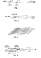
- Figure 1 illustrates a prior art method for aligning multiple lasers along a single optical path
- Figure 2 is an arrangement of a single laser diode mounted on a heat sink
- Figure 3 is a schematic of an array of laser diodes mounted in parallel
- Figure 4 is a prior art diode structure for amplifying a single wavelength
- Figures 5a and 5b show an axial array of laser diodes mounted on a heat sink according to the present invention
- Figure 6 illustrates an Li-L6 axial array according to the present invention using broad-beam emitters
- Figure 7 details the application of the present invention to a parallel array of axially-aligned laser diodes mounted on a heat sink;
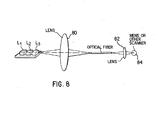
- Figure 8 illustrates scanning of an axial array of laser diodes into an optical fiber for a micro-electro-mechanical-system (MEMS) or other scanning device;
- MEMS micro-electro-mechanical-system
- Figures 9a and 9b show an example of deflective scanning using the laser diode system of the present invention.
- first laser diode L1 passes directly into the high reflector (HR) of a second laser diode L2 through the gain medium and out from the Output Coupler (OC). Additionally, the emission of the second laser L2 is also output from the OC of the second laser. The coincident beams of lasers L1 and L2 are then directed into the High-Reflector (HR) and out from the Output Coupler (OC) of an additional laser diode L3 in a sequential fashion.
- HR high reflector
- OC Output Coupler
- the light from the Output Coupler of laser diode L3 thus includes superimposed beams from all three lasers (L1, L2, L3), which are aligned on a single optical axis.
- Light will propagate through the entire structure in a manner similar to that in which light passes through an optical fiber provided that individual laser diodes L1-L3 are directly adjacent to each other or separated by a very small distance.
- the beam from L1 passes directly through L2 and L3 and the beam from L2 passes directly through L3 along with the light beam emitted from L3. Therefore, all beams exit from the Output Coupler of the final diode L3, having diffraction properties of the final exit aperture yet retaining their original individual wavelengths.
- minor misalignments of the beams as they enter the subsequent lasers will be corrected by the confinement structure of the next diode.
- the functioning of the different wavelength laser diodes to provide through put optical alignment of the output beams results from the close end-to-end positioning of the individual devices and from the mirror coatings which make up the HR (high-reflector) and the OC (output coupler) of the diode.
- These coatings have very narrow band reflectivity (typically less than 10 nm FWHM (Full Width Half Minimum)).
- the facet coatings are transparent outside of the particular narrow band region thereby allowing light of other wavelengths to pass directly through the diode structure without heating up the surfaces, without lasing or oscillating, without depleting gain, or without interfering with the internal mode structure.
- any sequential laser functions to prevent diffraction of any proceeding laser beam(s) until it exits from the output coupler (OC) of the last diode in the series.
- OC output coupler
- the alignment mechanism described above and shown in Figures 5A and 5B can be used on a variety of structures including, but not limited to, standard Fabre-Perot lasers, and broad-beam emitters as shown in Figure 6. Furthermore, it is possible to construct arrays of such devices as shown in Figure 7.
- Figure 8 illustrates axially aligned laser diodes according to the present invention coupled into an optical fiber through the lens 80 and from the fiber through lens 82 into a scanner 84.
- An optical system according to the present invention provides low-cost optical subassemblies for laser projection displays and up -or down- conversion displays which are designed for automobiles.
- the invention may also be used in telecommunication systems, laser printing, volumnmetric displays and other products that incorporate laser diodes of multiple, differing wavelengths.
- Figures 9a and 9b illustrate axially aligned laser diodes according to the present invention which are coupled into a deflective scanning system and projected to form a display.
- Lens system 10 is used to focus the light from the aligned lasers 20 into the scanner aperture 40, and lens system 30 is used to provide post scanner beam control.
- Appropriate scanners for this implementation include mechanical scanners, galvanometer scanners, MEMs scanners, polygon scanners, acousto-optic modulators, and others. Modulation control of the individual lasers while they are being scanned across the screen enables multicolored visual information and text to be addressed at >30 Hz refresh rates.
Landscapes
- Physics & Mathematics (AREA)
- Optics & Photonics (AREA)
- Condensed Matter Physics & Semiconductors (AREA)
- General Physics & Mathematics (AREA)
- Electromagnetism (AREA)
- Engineering & Computer Science (AREA)
- Multimedia (AREA)
- Signal Processing (AREA)
- Semiconductor Lasers (AREA)
- Devices For Indicating Variable Information By Combining Individual Elements (AREA)
- Mechanical Optical Scanning Systems (AREA)
- Optical Couplings Of Light Guides (AREA)
Abstract
Description
Claims (37)
- A laser diode system for propagating multiple laser beams of different wavelengths along the same optical axis, the system comprising:at least two laser diodes; andlaser support structure for supporting said at least two laser diodes in a substantial abutting relationship, wherein each of said at least two laser diodes output a wavelength different from any other one of said at least two laser diodes and wherein an output of one of said at least two laser diodes provides a laser output containing beams from each of said at least two laser diodes, said contained beams retaining their original wavelengths and being aligned in the same optical axis.
- The system according to claim 1 wherein each of said at least two diode includes a first reflective coating on a back facet and a second reflective coating on a front facet.
- The system according to claim 1 wherein at least one of said at least two diode outputs a visible wavelength.
- The system according to claim 1 wherein at least one of said two diode outputs an ultra-violet wavelength.
- The system according to claim 1 wherein said or at least two diode outputs an infrared wavelength.
- The system according to claim 1, wherein said laser support is a heat sink.
- The diode system according to claim 2, wherein the first and second reflective coatings of the front facet and the rear facet provide very narrow band reflectivity with said coatings being transparent outside of said narrow band thereby allowing light of wavelengths outside said narrow band to pass directly through the diode.
- The system according to claim 1, wherein diffraction properties of each of said beams in said output are provided as a function of a final exit aperture of said one laser diode.
- The system according to claim 1, wherein each of said at least two laser diodes are Fabre-Perot lasers.
- The system according to claim 1, wherein each of said at least two lasers are broad-beam emitter lasers.
- The system according to claim 1, wherein the laser diodes have antireflection facet coatings at wavelengths outside of a lasing band of each device.
- A method for aligning multiple laser beams along an optical axis, the method comprising the acts of:providing a plurality of laser diodes;coating a back facet and a front facet of each of said plurality of diodes;arranging said plurality of diodes in a substantially sequential relationship on a support structure whereby a resulting laser output contains a laser beam output from each of said plurality of diodes and wherein each of said output laser beams is aligned in a same single optical axis.
- The method according to claim 12, further including fixing each of said laser diodes onto a heat sink.
- The method according to claim 13, wherein fixing includes soldering the laser diodes to the heat sink.
- The method according to claim 13, further including hermetically encasing said plurality of laser diodes on said heat sink.
- The method according to claim 12, wherein said coated front and back facet of said plurality of diodes provides a narrow band reflectivity, which allows light of wavelengths outside said narrow band to pass directly through.
- The method according to claim 16, wherein the coating of the rear facet provides substantially 100 % reflectivity of the laser wavelength and the coating of the front facet provides less than 100% reflectivity by design.
- An optically aligned arrangement of laser diodes, comprising:a plurality of laser diodes with each of said laser diodes outputting different wavelengths;a support device retaining said plurality of laser diodes in a series of back-two-back substantially abutting relationships, each of said plurality of laser diode having front and back coated facets wherein one of said plurality of laser diodes outputs a plurality of laser beams, wherein each of said plurality of laser beams respectively corresponds to each of said plurality of laser diodes, and wherein each of said laser beams proceeds from said one laser diode in a single same optical axis.
- The arrangement according to claim 18, wherein said output plurality of beams provide an input to a deflective scanner.
- The arrangement according to claim 19, wherein the deflective scanner is at least one of a MEMS scanner, a mechanical scanner, a galvanometer scanner, a polygon scanner, an acousto-optic modulator.
- The arrangement according to claim 18, wherein said output plurality of beams provide input to a deflective scanner, wherein the output of the deflective scanner provides displayed information on a viewing screen.
- The arrangement according to claim 21, wherein said viewing screen is reflective of visible colors.
- The arrangement according to claim 21, wherein said viewing screen is a phosphor screen.
- The arrangement according to claim 23, wherein said phosphor viewing screen is a Stokes fluorescent phosphor viewing screen.
- The arrangement according to claim 22, wherein said phosphor viewing screen is an upconversion phosphor viewing screen.
- The arrangement according to claim 18, wherein said output plurality of beams are modified with additional optical elements to appropriately shape said output beams for input into a defective scanning system.
- The arrangements according to claim 26, wherein said optical elements are lenses.
- The arrangement according to claim 18, wherein said output plurality of beams are additionally modified with post scanner optical elements to appropriately shape and correct the displayed information on the phosphor screen.
- The arrangement according to claim 28, wherein the post scanner optical elements are lenses.
- The arrangement according to claim 18, wherein said support device is a heat sink.
- The arrangement according to claim 30, wherein said heat sink is integrated with a thermal electric Peltier cooler and a thermister for monitoring and maintaining the proper temperature of the device.
- The arrangement according to claim 18, wherein said output beams provide an optical fiber input.
- The arrangement according to claim 32, further including an optical fiber for receiving said optical fiber input and outputting a fiber output to a scanning device.
- The arrangement according to claim 32, further including an optical fiber for receiving said optical fiber input and providing an output to a micro-electro-mechanical-system projection display device.
- The arrangement according to claim 25 wherein said upconversion viewing screen function with a single frequency upconversion.
- The arrangement according to claim 25 wherein said upconversion viewing screen functions with a gated-two frequency upconversion.
- A laser diode system, comprising:at least two individual laser diodes aligned one behind the other, a first of said two laser diodes outputting a first laser beam of a first wavelength along an optical axis into a second of said two laser diodes; andwherein the second laser diode outputs a laser beam containing the first and a second, different, wavelength along the optical axis.
Applications Claiming Priority (4)
| Application Number | Priority Date | Filing Date | Title |
|---|---|---|---|
| US10/767,199 US20050169581A1 (en) | 2004-01-30 | 2004-01-30 | Laser diode system |
| US767199 | 2004-01-30 | ||
| US10/948,757 US7376165B2 (en) | 2004-01-30 | 2004-09-24 | Laser diode alignment and packaging system for integrated optical and display subassemblies |
| US948757 | 2004-09-24 |
Publications (3)
| Publication Number | Publication Date |
|---|---|
| EP1605564A2 true EP1605564A2 (en) | 2005-12-14 |
| EP1605564A3 EP1605564A3 (en) | 2007-09-19 |
| EP1605564B1 EP1605564B1 (en) | 2019-01-02 |
Family
ID=34915767
Family Applications (1)
| Application Number | Title | Priority Date | Filing Date |
|---|---|---|---|
| EP05001783.9A Ceased EP1605564B1 (en) | 2004-01-30 | 2005-01-28 | Laser diode alignment and packaging system for integrated optical and display subassemblies |
Country Status (3)
| Country | Link |
|---|---|
| US (1) | US7376165B2 (en) |
| EP (1) | EP1605564B1 (en) |
| JP (1) | JP2005217401A (en) |
Families Citing this family (4)
| Publication number | Priority date | Publication date | Assignee | Title |
|---|---|---|---|---|
| EP2434594B1 (en) * | 2010-09-27 | 2014-05-14 | Alcatel Lucent | Photonic integrated circuit for wavelength division multiplexing |
| US12152858B2 (en) | 2014-12-23 | 2024-11-26 | Jm Acquisitions Inc | Aiming device for a firearm |
| DE102015118715A1 (en) * | 2015-11-02 | 2017-05-04 | Osram Opto Semiconductors Gmbh | Semiconductor laser array and projector |
| US11710942B2 (en) * | 2017-12-13 | 2023-07-25 | Sony Corporation | Method of manufacturing light-emitting module, light-emitting module, and device |
Family Cites Families (25)
| Publication number | Priority date | Publication date | Assignee | Title |
|---|---|---|---|---|
| US3896473A (en) | 1973-12-04 | 1975-07-22 | Bell Telephone Labor Inc | Gallium arsenide schottky barrier avalance diode array |
| JPS58196634A (en) * | 1982-05-12 | 1983-11-16 | Nec Corp | Light source for optical head |
| JPS5946662B2 (en) | 1982-05-13 | 1984-11-14 | 株式会社 品川工業所 | Continuous stirring device |
| JPH0824207B2 (en) * | 1987-01-12 | 1996-03-06 | 三菱電機株式会社 | Semiconductor laser device |
| JP2819160B2 (en) * | 1989-08-03 | 1998-10-30 | 日本電信電話株式会社 | Multi-wavelength semiconductor laser diode |
| JPH04171778A (en) * | 1990-11-05 | 1992-06-18 | Hoya Corp | Solid-state laser device |
| JP3149961B2 (en) * | 1991-01-30 | 2001-03-26 | キヤノン株式会社 | Multi-wavelength semiconductor laser device and driving method thereof |
| US5265115A (en) * | 1991-08-30 | 1993-11-23 | Hoya Corporation | Solid-state laser device having a feedback loop |
| SE501721C2 (en) * | 1993-09-10 | 1995-05-02 | Ellemtel Utvecklings Ab | Laser device with an optical cavity connected in series laser structures |
| US5430748A (en) | 1994-01-21 | 1995-07-04 | Maccormack; Stuart | Laser system with phase-conjugator-enhanced output |
| US5914976A (en) | 1997-01-08 | 1999-06-22 | W. L. Gore & Associates, Inc. | VCSEL-based multi-wavelength transmitter and receiver modules for serial and parallel optical links |
| JPH1117279A (en) * | 1997-06-20 | 1999-01-22 | Toshiba Corp | WDM optical communication device, transmitter, receiver, and WDM optical communication system |
| US6104739A (en) | 1997-12-24 | 2000-08-15 | Nortel Networks Corporation | Series of strongly complex coupled DFB lasers |
| JPH11305707A (en) * | 1998-04-20 | 1999-11-05 | Nippon Signal Co Ltd:The | In-vehicle display device |
| JP2000138421A (en) * | 1998-10-30 | 2000-05-16 | Sharp Corp | Semiconductor laser device |
| JP2000147312A (en) | 1998-11-10 | 2000-05-26 | Furukawa Electric Co Ltd:The | Laser module and manufacturing method thereof |
| JP2001185811A (en) * | 1999-12-24 | 2001-07-06 | Sanyo Electric Co Ltd | Semiconductor laser device |
| JP2001185819A (en) * | 1999-12-27 | 2001-07-06 | Sankyo Seiki Mfg Co Ltd | Laser light source device and optical pickup device |
| JP4589539B2 (en) * | 2000-02-18 | 2010-12-01 | パナソニック株式会社 | Semiconductor laser device and manufacturing method thereof |
| JP2002148554A (en) | 2000-11-03 | 2002-05-22 | Samsung Electronics Co Ltd | Optical scanner, laser image projection apparatus using the same, and method of driving the same |
| JP4617600B2 (en) * | 2001-05-02 | 2011-01-26 | ソニー株式会社 | Two-wavelength semiconductor laser device |
| DE10147353C2 (en) * | 2001-09-26 | 2003-12-18 | Infineon Technologies Ag | Semiconductor laser with at least two optically active areas |
| JP2003179315A (en) * | 2001-12-12 | 2003-06-27 | Seiko Epson Corp | Optical module and optical communication system |
| JP2003195125A (en) * | 2001-12-27 | 2003-07-09 | Seiko Epson Corp | Optical module and optical communication system |
| DE10227468A1 (en) * | 2002-06-20 | 2004-01-15 | Bayerische Motoren Werke Ag | Projection system and method |
-
2004
- 2004-09-24 US US10/948,757 patent/US7376165B2/en not_active Expired - Lifetime
-
2005
- 2005-01-19 JP JP2005011914A patent/JP2005217401A/en active Pending
- 2005-01-28 EP EP05001783.9A patent/EP1605564B1/en not_active Ceased
Also Published As
| Publication number | Publication date |
|---|---|
| US7376165B2 (en) | 2008-05-20 |
| EP1605564B1 (en) | 2019-01-02 |
| US20050169337A1 (en) | 2005-08-04 |
| JP2005217401A (en) | 2005-08-11 |
| EP1605564A3 (en) | 2007-09-19 |
Similar Documents
| Publication | Publication Date | Title |
|---|---|---|
| US7296897B2 (en) | Projection display apparatus, system, and method | |
| US6945652B2 (en) | Projection display device | |
| US6900916B2 (en) | Color laser display apparatus having fluorescent screen scanned with modulated ultraviolet laser light | |
| US6612703B2 (en) | Spectrally beam combined display system | |
| WO1995020811A1 (en) | Laser illuminated display system | |
| EP1381241A2 (en) | Display device | |
| CA2089615A1 (en) | Laser light beam generating apparatus | |
| JPH09504920A (en) | High resolution image projection system and method using a laser | |
| US20080259247A1 (en) | Laser backlighting for displays | |
| US7586971B2 (en) | External-cavity laser light source apparatus and laser light emission module | |
| US7376165B2 (en) | Laser diode alignment and packaging system for integrated optical and display subassemblies | |
| KR101455800B1 (en) | Laser diode module and optical structure for use therein | |
| US6606332B1 (en) | Method and apparatus of color mixing in a laser diode system | |
| US7190497B2 (en) | Scanning type image display optical system, scanning type image display apparatus, and image display system | |
| WO1990013158A1 (en) | Close packed, end face, diode pumped, fibre laser bundle, phased-array laser oscillator | |
| JP2023528429A (en) | Light source system and laser projection display | |
| US20050169581A1 (en) | Laser diode system | |
| JP2005217401A5 (en) | ||
| JPH1197779A (en) | Multicolor light modulation amplifier and projection display device using the same | |
| US7901106B2 (en) | Solid-state illuminator for display applications | |
| CN115469503B (en) | Projection system with combination of laser and LED light source | |
| KR100879974B1 (en) | Multi laser module package | |
| US11815677B1 (en) | Display using scanning-based sequential pupil expansion | |
| US6621549B1 (en) | Fiber optic flat panel liquid crystal display | |
| Kent et al. | Lightweight helmet-mounted night vision and FLIR imagery display systems |
Legal Events
| Date | Code | Title | Description |
|---|---|---|---|
| PUAI | Public reference made under article 153(3) epc to a published international application that has entered the european phase |
Free format text: ORIGINAL CODE: 0009012 |
|
| AK | Designated contracting states |
Kind code of ref document: A2 Designated state(s): AT BE BG CH CY CZ DE DK EE ES FI FR GB GR HU IE IS IT LI LT LU MC NL PL PT RO SE SI SK TR |
|
| AX | Request for extension of the european patent |
Extension state: AL BA HR LV MK YU |
|
| PUAL | Search report despatched |
Free format text: ORIGINAL CODE: 0009013 |
|
| AK | Designated contracting states |
Kind code of ref document: A3 Designated state(s): AT BE BG CH CY CZ DE DK EE ES FI FR GB GR HU IE IS IT LI LT LU MC NL PL PT RO SE SI SK TR |
|
| AX | Request for extension of the european patent |
Extension state: AL BA HR LV MK YU |
|
| 17P | Request for examination filed |
Effective date: 20080313 |
|
| AKX | Designation fees paid |
Designated state(s): DE ES FR GB IT SE |
|
| RAP1 | Party data changed (applicant data changed or rights of an application transferred) |
Owner name: 3D TECHNOLOGY LABORATORIES, INC. Owner name: BAYERISCHE MOTOREN WERKE AKTIENGESELLSCHAFT |
|
| 17Q | First examination report despatched |
Effective date: 20151021 |
|
| GRAP | Despatch of communication of intention to grant a patent |
Free format text: ORIGINAL CODE: EPIDOSNIGR1 |
|
| RIC1 | Information provided on ipc code assigned before grant |
Ipc: H01S 5/028 20000101ALN20180719BHEP Ipc: H01S 5/50 20000101ALN20180719BHEP Ipc: H01S 5/40 20000101AFI20180719BHEP Ipc: H01S 5/00 20000101ALN20180719BHEP Ipc: H04N 9/31 19740701ALN20180719BHEP Ipc: H01S 5/022 20000101ALI20180719BHEP Ipc: H01S 5/024 20000101ALI20180719BHEP |
|
| INTG | Intention to grant announced |
Effective date: 20180801 |
|
| GRAS | Grant fee paid |
Free format text: ORIGINAL CODE: EPIDOSNIGR3 |
|
| GRAA | (expected) grant |
Free format text: ORIGINAL CODE: 0009210 |
|
| AK | Designated contracting states |
Kind code of ref document: B1 Designated state(s): DE ES FR GB IT SE |
|
| REG | Reference to a national code |
Ref country code: GB Ref legal event code: FG4D |
|
| REG | Reference to a national code |
Ref country code: DE Ref legal event code: R096 Ref document number: 602005055217 Country of ref document: DE |
|
| RIC2 | Information provided on ipc code assigned after grant |
Ipc: H01S 5/022 20060101ALI20180719BHEP Ipc: H01S 5/50 20060101ALN20180719BHEP Ipc: H01S 5/024 20060101ALI20180719BHEP Ipc: H04N 9/31 20060101ALN20180719BHEP Ipc: H01S 5/00 20060101ALN20180719BHEP Ipc: H01S 5/40 20060101AFI20180719BHEP Ipc: H01S 5/028 20060101ALN20180719BHEP |
|
| PGFP | Annual fee paid to national office [announced via postgrant information from national office to epo] |
Ref country code: CH Payment date: 20190124 Year of fee payment: 8 |
|
| PG25 | Lapsed in a contracting state [announced via postgrant information from national office to epo] |
Ref country code: ES Free format text: LAPSE BECAUSE OF FAILURE TO SUBMIT A TRANSLATION OF THE DESCRIPTION OR TO PAY THE FEE WITHIN THE PRESCRIBED TIME-LIMIT Effective date: 20190102 Ref country code: SE Free format text: LAPSE BECAUSE OF FAILURE TO SUBMIT A TRANSLATION OF THE DESCRIPTION OR TO PAY THE FEE WITHIN THE PRESCRIBED TIME-LIMIT Effective date: 20190102 |
|
| REG | Reference to a national code |
Ref country code: DE Ref legal event code: R097 Ref document number: 602005055217 Country of ref document: DE |
|
| PG25 | Lapsed in a contracting state [announced via postgrant information from national office to epo] |
Ref country code: IT Free format text: LAPSE BECAUSE OF FAILURE TO SUBMIT A TRANSLATION OF THE DESCRIPTION OR TO PAY THE FEE WITHIN THE PRESCRIBED TIME-LIMIT Effective date: 20190102 |
|
| PLBE | No opposition filed within time limit |
Free format text: ORIGINAL CODE: 0009261 |
|
| STAA | Information on the status of an ep patent application or granted ep patent |
Free format text: STATUS: NO OPPOSITION FILED WITHIN TIME LIMIT |
|
| 26N | No opposition filed |
Effective date: 20191003 |
|
| PGFP | Annual fee paid to national office [announced via postgrant information from national office to epo] |
Ref country code: GB Payment date: 20200127 Year of fee payment: 16 |
|
| PGFP | Annual fee paid to national office [announced via postgrant information from national office to epo] |
Ref country code: FR Payment date: 20200123 Year of fee payment: 16 |
|
| REG | Reference to a national code |
Ref country code: DE Ref legal event code: R119 Ref document number: 602005055217 Country of ref document: DE |
|
| PG25 | Lapsed in a contracting state [announced via postgrant information from national office to epo] |
Ref country code: DE Free format text: LAPSE BECAUSE OF NON-PAYMENT OF DUE FEES Effective date: 20200801 |
|
| GBPC | Gb: european patent ceased through non-payment of renewal fee |
Effective date: 20210128 |
|
| PG25 | Lapsed in a contracting state [announced via postgrant information from national office to epo] |
Ref country code: FR Free format text: LAPSE BECAUSE OF NON-PAYMENT OF DUE FEES Effective date: 20210131 |
|
| PG25 | Lapsed in a contracting state [announced via postgrant information from national office to epo] |
Ref country code: GB Free format text: LAPSE BECAUSE OF NON-PAYMENT OF DUE FEES Effective date: 20210128 |