EP1605521A2 - Manufacturing method for a base piece made to adhere to an adhesive sheet, for a semiconductor wafer and for a semiconductor device - Google Patents
Manufacturing method for a base piece made to adhere to an adhesive sheet, for a semiconductor wafer and for a semiconductor device Download PDFInfo
- Publication number
- EP1605521A2 EP1605521A2 EP05253596A EP05253596A EP1605521A2 EP 1605521 A2 EP1605521 A2 EP 1605521A2 EP 05253596 A EP05253596 A EP 05253596A EP 05253596 A EP05253596 A EP 05253596A EP 1605521 A2 EP1605521 A2 EP 1605521A2
- Authority
- EP
- European Patent Office
- Prior art keywords
- adhesive sheet
- adhere
- base
- glass
- pieces
- Prior art date
- Legal status (The legal status is an assumption and is not a legal conclusion. Google has not performed a legal analysis and makes no representation as to the accuracy of the status listed.)
- Withdrawn
Links
Images




Classifications
-
- H—ELECTRICITY
- H10—SEMICONDUCTOR DEVICES; ELECTRIC SOLID-STATE DEVICES NOT OTHERWISE PROVIDED FOR
- H10F—INORGANIC SEMICONDUCTOR DEVICES SENSITIVE TO INFRARED RADIATION, LIGHT, ELECTROMAGNETIC RADIATION OF SHORTER WAVELENGTH OR CORPUSCULAR RADIATION
- H10F39/00—Integrated devices, or assemblies of multiple devices, comprising at least one element covered by group H10F30/00, e.g. radiation detectors comprising photodiode arrays
- H10F39/80—Constructional details of image sensors
- H10F39/804—Containers or encapsulations
-
- H—ELECTRICITY
- H10—SEMICONDUCTOR DEVICES; ELECTRIC SOLID-STATE DEVICES NOT OTHERWISE PROVIDED FOR
- H10P—GENERIC PROCESSES OR APPARATUS FOR THE MANUFACTURE OR TREATMENT OF DEVICES COVERED BY CLASS H10
- H10P54/00—Cutting or separating of wafers, substrates or parts of devices
-
- H—ELECTRICITY
- H10—SEMICONDUCTOR DEVICES; ELECTRIC SOLID-STATE DEVICES NOT OTHERWISE PROVIDED FOR
- H10P—GENERIC PROCESSES OR APPARATUS FOR THE MANUFACTURE OR TREATMENT OF DEVICES COVERED BY CLASS H10
- H10P72/00—Handling or holding of wafers, substrates or devices during manufacture or treatment thereof
- H10P72/70—Handling or holding of wafers, substrates or devices during manufacture or treatment thereof for supporting or gripping
- H10P72/74—Handling or holding of wafers, substrates or devices during manufacture or treatment thereof for supporting or gripping using temporarily an auxiliary support
-
- H—ELECTRICITY
- H10—SEMICONDUCTOR DEVICES; ELECTRIC SOLID-STATE DEVICES NOT OTHERWISE PROVIDED FOR
- H10W—GENERIC PACKAGES, INTERCONNECTIONS, CONNECTORS OR OTHER CONSTRUCTIONAL DETAILS OF DEVICES COVERED BY CLASS H10
- H10W76/00—Containers; Fillings or auxiliary members therefor; Seals
- H10W76/10—Containers or parts thereof
-
- H—ELECTRICITY
- H10—SEMICONDUCTOR DEVICES; ELECTRIC SOLID-STATE DEVICES NOT OTHERWISE PROVIDED FOR
- H10F—INORGANIC SEMICONDUCTOR DEVICES SENSITIVE TO INFRARED RADIATION, LIGHT, ELECTROMAGNETIC RADIATION OF SHORTER WAVELENGTH OR CORPUSCULAR RADIATION
- H10F39/00—Integrated devices, or assemblies of multiple devices, comprising at least one element covered by group H10F30/00, e.g. radiation detectors comprising photodiode arrays
- H10F39/10—Integrated devices
- H10F39/12—Image sensors
-
- H—ELECTRICITY
- H10—SEMICONDUCTOR DEVICES; ELECTRIC SOLID-STATE DEVICES NOT OTHERWISE PROVIDED FOR
- H10F—INORGANIC SEMICONDUCTOR DEVICES SENSITIVE TO INFRARED RADIATION, LIGHT, ELECTROMAGNETIC RADIATION OF SHORTER WAVELENGTH OR CORPUSCULAR RADIATION
- H10F39/00—Integrated devices, or assemblies of multiple devices, comprising at least one element covered by group H10F30/00, e.g. radiation detectors comprising photodiode arrays
- H10F39/10—Integrated devices
- H10F39/12—Image sensors
- H10F39/15—Charge-coupled device [CCD] image sensors
-
- H—ELECTRICITY
- H10—SEMICONDUCTOR DEVICES; ELECTRIC SOLID-STATE DEVICES NOT OTHERWISE PROVIDED FOR
- H10F—INORGANIC SEMICONDUCTOR DEVICES SENSITIVE TO INFRARED RADIATION, LIGHT, ELECTROMAGNETIC RADIATION OF SHORTER WAVELENGTH OR CORPUSCULAR RADIATION
- H10F39/00—Integrated devices, or assemblies of multiple devices, comprising at least one element covered by group H10F30/00, e.g. radiation detectors comprising photodiode arrays
- H10F39/80—Constructional details of image sensors
- H10F39/806—Optical elements or arrangements associated with the image sensors
- H10F39/8063—Microlenses
-
- H—ELECTRICITY
- H10—SEMICONDUCTOR DEVICES; ELECTRIC SOLID-STATE DEVICES NOT OTHERWISE PROVIDED FOR
- H10P—GENERIC PROCESSES OR APPARATUS FOR THE MANUFACTURE OR TREATMENT OF DEVICES COVERED BY CLASS H10
- H10P72/00—Handling or holding of wafers, substrates or devices during manufacture or treatment thereof
- H10P72/70—Handling or holding of wafers, substrates or devices during manufacture or treatment thereof for supporting or gripping
- H10P72/74—Handling or holding of wafers, substrates or devices during manufacture or treatment thereof for supporting or gripping using temporarily an auxiliary support
- H10P72/7416—Handling or holding of wafers, substrates or devices during manufacture or treatment thereof for supporting or gripping using temporarily an auxiliary support used during dicing or grinding
- H10P72/7418—Handling or holding of wafers, substrates or devices during manufacture or treatment thereof for supporting or gripping using temporarily an auxiliary support used during dicing or grinding of passive members, e.g. a chip mounting substrate
-
- H—ELECTRICITY
- H10—SEMICONDUCTOR DEVICES; ELECTRIC SOLID-STATE DEVICES NOT OTHERWISE PROVIDED FOR
- H10P—GENERIC PROCESSES OR APPARATUS FOR THE MANUFACTURE OR TREATMENT OF DEVICES COVERED BY CLASS H10
- H10P72/00—Handling or holding of wafers, substrates or devices during manufacture or treatment thereof
- H10P72/70—Handling or holding of wafers, substrates or devices during manufacture or treatment thereof for supporting or gripping
- H10P72/74—Handling or holding of wafers, substrates or devices during manufacture or treatment thereof for supporting or gripping using temporarily an auxiliary support
- H10P72/7434—Handling or holding of wafers, substrates or devices during manufacture or treatment thereof for supporting or gripping using temporarily an auxiliary support used in a transfer process involving at least two transfer steps, i.e. including an intermediate handle substrate
-
- Y—GENERAL TAGGING OF NEW TECHNOLOGICAL DEVELOPMENTS; GENERAL TAGGING OF CROSS-SECTIONAL TECHNOLOGIES SPANNING OVER SEVERAL SECTIONS OF THE IPC; TECHNICAL SUBJECTS COVERED BY FORMER USPC CROSS-REFERENCE ART COLLECTIONS [XRACs] AND DIGESTS
- Y10—TECHNICAL SUBJECTS COVERED BY FORMER USPC
- Y10T—TECHNICAL SUBJECTS COVERED BY FORMER US CLASSIFICATION
- Y10T156/00—Adhesive bonding and miscellaneous chemical manufacture
- Y10T156/10—Methods of surface bonding and/or assembly therefor
- Y10T156/1052—Methods of surface bonding and/or assembly therefor with cutting, punching, tearing or severing
Definitions
- the present invention relates to a method for manufacturing a number of base pieces, such as glass pieces or pieces of silicon substrate that are made to adhere to an adhesive sheet, as well as to a manufacturing method for a semiconductor wafer and a manufacturing method for a semiconductor device which utilize this manufacturing method for base pieces that are made to adhere to an adhesive sheet.
- FIGS. 1A and 1B are diagrams showing conventional steps for manufacturing glass pieces.
- An adhesive sheet 41 is made to adhere to glass 42 in plate form (FIG. 1A).
- glass 42 is cut using a blade 43, so as to be separated into a number of pieces of glass 42a (FIG. 1B).
- the separated pieces of glass 42a are one by one peeled from adhesive sheet 41, and are utilized as lids of, for example, packages of semiconductor elements.
- FIG. 2 is an enlarged diagram of region A in FIG. 1B.
- Glass chips 45 are created at the time of cutting of glass 42 as shown in FIG. 1B.
- the created glass chips 45 are attached to glass pieces 42a due to static electricity.
- these glass chips 45 sometimes cause a defect in the semiconductor device. Accordingly, it is necessary to remove the created glass chips 45 so that glass chips 45 do not adhere to pieces of glass 42a.
- a means for removing glass chips 45 through the blowing of a gas or by washing with water has conventionally been carried out, wherein a problem arises where a gas or water for removing the chips do not sufficiently reach particularly the corner portions (regions B in FIG. 2) of the cut parts, and glass chips 45 are not completely removed and are left in the corner portions.
- the present invention is provided in view of the above described situation and an object thereof is to provide a manufacturing method for a base piece made to adhere to an adhesive sheet where base chips that are created at the time of cutting of a base such as glass can be easily and almost completely removed.
- Another object of the present invention is to provide a manufacturing method for a base piece made to adhere to an adhesive sheet where debris that adheres to a film that has been formed on one surface of a base piece can be removed.
- Still another object of the present invention is to provide a manufacturing method for a semiconductor wafer and a manufacturing method for a semiconductor device where occurrence of defects caused by base chips can be restricted.
- a base that is made to adhere to a first adhesive sheet is cut into a number of base pieces and a second adhesive sheet is made to adhere to the surfaces of the base pieces on the side opposite to the surfaces which are made to adhere to the first adhesive sheet.
- the base that is made to adhere to the first adhesive sheet is cut into a number of base pieces, and after that, the second adhesive sheet is made to adhere to the surfaces of the base pieces on the side opposite to the surfaces which are made to adhere to the first adhesive sheet.
- a base that is made to adhere to a first adhesive sheet is cut into a number of base pieces, a second adhesive sheet is made to adhere to the surfaces of the base pieces on the side opposite to the surfaces which are made to adhere to the first adhesive sheet, and the first adhesive sheet is peeled from the base pieces.
- the base that is made to adhere to the first adhesive sheet is cut into a number of base pieces, and after that, the second adhesive sheet is made to adhere to the surfaces of the base pieces on the side opposite to the surfaces which are made to adhere to the first adhesive sheet, and then the first adhesive sheet is peeled from the base pieces. Accordingly, almost all of the base chips that have occurred at the time of cutting, including the base chips which are placed in the corner portions of the cut parts, can be easily removed in the state of adhering to the first adhesive sheet.
- a film has been formed on the surface of the base on the side opposite to the surface which is made to adhere to the first adhesive sheet, and after the first adhesive sheet is peeled, a third adhesive sheet is made to adhere to the surfaces of the base pieces to which the first adhesive sheet has been made to adhere, in the above described manufacturing method.
- the third adhesive sheet is made to adhere to the surface on the side to which the first adhesive sheet has been made to adhere after the first adhesive sheet is peeled.
- a film has been formed on the surface of the base on the side opposite to the surface which is made to adhere to the first adhesive sheet, and after the first adhesive sheet is peeled, a third adhesive sheet is made to adhere to the surfaces of the base pieces to which the first adhesive sheet has been made to adhere and the second adhesive sheet is peeled from the base pieces in the above described manufacturing method.
- the third adhesive sheet is made to adhere to the surface on the side to which the first adhesive sheet has been made to adhere, and then, the second adhesive sheet is peeled from the base pieces after the first adhesive sheet has been peeled. Accordingly, debris that has adhered to the films on the base pieces is easily removed in the state of adhering to the second adhesive sheet.
- a base that is made to adhere to a first adhesive sheet is cut into a number of base pieces, a second adhesive sheet is made to adhere to the surfaces of the base pieces on the side opposite to the surfaces which are made to adhere to the first adhesive sheet, the first adhesive sheet is peeled from the base pieces, and the base pieces are removed from the second adhesive sheet and are made to adhere to a semiconductor wafer.
- the base that is made to adhere to the first adhesive sheet is cut into a number of base pieces, and after that, the second adhesive sheet is made to adhere to the surfaces of the base pieces on the side opposite to the surfaces which are made to adhere to the first adhesive sheet, and then the first adhesive sheet is peeled from the base pieces and the base pieces that have been peeled from the second adhesive sheet are made to adhere to the semiconductor wafer. Accordingly, base chips are almost completely removed together with the first adhesive sheet, and thus, base pieces to which almost no base chips are attached are made to adhere to the semiconductor wafer, and therefore, no defects are caused by base chips.
- a base that is made to adhere to a first adhesive sheet is cut into a number of base pieces, a second adhesive sheet is made to adhere to the surfaces of the base pieces on the side opposite to the surfaces which are made to adhere to the first adhesive sheet, the first adhesive sheet is peeled from the base pieces, the base pieces are removed from the second adhesive sheet and are made to adhere to a semiconductor wafer, and this semiconductor wafer is cut into pieces.
- the base that is made to adhere to the first adhesive sheet is cut into a number of base pieces, and after that, the second adhesive sheet is made to adhere to the surfaces of the base pieces on the side opposite to the surfaces which are made to adhere to the first adhesive sheet, and then the first adhesive sheet is peeled from the base pieces and the base pieces that have been peeled from the second adhesive sheet are made to adhere to the semiconductor wafer and the semiconductor wafer is cut into pieces. Accordingly, base chips are almost completely removed together with the first adhesive sheet, and thus, base pieces to which almost no base chips are attached are made to adhere to the semiconductor wafer, and therefore, no defective semiconductor devices are caused by base chips.
- a base that is made to adhere to a first adhesive sheet is cut into a number of base pieces, a second adhesive sheet is made to adhere to the surfaces of the base pieces on the side opposite to the surfaces which are made to adhere to the first adhesive sheet, the first adhesive sheet is peeled from the base pieces, and the base piece is removed from the second adhesive sheet and is made to adhere to a case member that contains a semiconductor element.
- the base that is made to adhere to the first adhesive sheet is cut into a number of base pieces, and after that, the second adhesive sheet is made to adhere to the surfaces of the base pieces on the side opposite to the surfaces which are made to adhere to the first adhesive sheet, and then the first adhesive sheet is peeled from the base pieces and the base piece that has been peeled from the second adhesive sheet is made to adhere to a case member that contains a semiconductor element. Accordingly, base chips are almost completely removed together with the first adhesive sheet, and thus, the base piece to which almost no base chips are attached is made to adhere to a case member, and therefore, no defects are caused by base chips.
- base chips are removed when the first adhesive sheet is peeled, and therefore, most of the base chips can be easily removed.
- debris that adheres to the film is removed when the second adhesive sheet is peeled, and therefore, most of the debris can be easily removed.
- the base piece to which almost no base chips adhere can be made to adhere, and therefore, occurrence of defects caused by base chips can be significantly restricted.
- FIGS. 3A to 3D are diagrams showing an example of a process that is in accordance with a manufacturing method for a base piece made to adhere to an adhesive sheet according to the present invention.
- the adhesive surface of a first adhesive sheet 1 is made to adhere to glass 2 in plate form (FIG. 3A).
- glass 2 is cut by a blade 3 using a dicing unit or the like, so as to be separated into a number of pieces of glass 2a (FIG. 3B).
- glass chips may be removed through the blowing of a gas (for example, blowing of nitrogen) if necessary.
- washing may be carried out, using a washing liquid, such as water or a solution, as long as first adhesive sheet 1 can maintain sufficient adhesiveness.
- a second adhesive sheet 4 is made to adhere to the surface of pieces of glass 2a on the side opposite to the side to which first adhesive sheet 1 is made to adhere (FIG. 3C).
- a base piece a piece of glass 2a, in the present example
- an adhesive sheet first adhesive sheet 1 and second adhesive sheet 4, in the present example
- adhesive sheets of which the adhesiveness is lowered through irradiation with light for example, irradiation with ultraviolet rays, can be used as the above described the first adhesive sheet 1 and the second adhesive sheet 4.
- the first adhesive sheet 1 is peeled from glass pieces 2a (FIG. 3D).
- a base piece a piece of glass 2a, in the present example
- an adhesive sheet second adhesive sheet 4, in the present example
- glass chips 5 are created as base chips on the cut parts during the process for cutting glass 2 (FIG. 3B). Created glass chips 5 adhere to the first adhesive sheet 1. Therefore, the first adhesive sheet 1 is peeled in the state where glass chips 5 adhere to the first adhesive sheet 1 after the second adhesive sheet 4 has been made to adhere to the pieces of glass. By doing so, it becomes possible to remove most of glass chips 5 by making them adhere to the first adhesive sheet 1 without breaking up respective pieces of glass 2a that are in the state where they adhere to the second adhesive sheet 4.
- glass chips 5 may be removed through the blowing of a gas.
- washing may be carried out using a washing liquid, such as water or a solution, as long as the second adhesive sheet 4 can maintain sufficient adhesiveness.
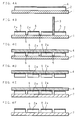
- FIGS. 4A to 4F are diagrams showing another example of a process that is in accordance with a manufacturing method for a base piece made to adhere to an adhesive sheet according to the present invention.
- the adhesive surface of a first adhesive sheet 1 is made to adhere to glass 2 in plate form (FIG. 4A).
- An infrared ray blocking film 6 is formed on the surface (surface on the side opposite to the surface to which the first adhesive sheet 1 adheres) of glass 2 using, for example, a physical vapor deposition method.
- glass 2 with infrared ray blocking film 6 is cut by a blade 3 using a dicing unit or the like, so as to be separated into a number of pieces of glass 2a (FIG. 4B).
- blowing of a gas or washing with a solution may be carried out, if necessary.
- the adhesive surface of a second adhesive sheet 4 is made to adhere to the surface of pieces of glass 2a on the side opposite to the surface to which the first adhesive sheet 1 adheres, that is to say, to the top of infrared ray blocking film 6 (FIG. 4C).
- adhesive sheets of which the adhesiveness is lowered through irradiation with light for example, irradiation with ultraviolet rays, can be used as the above described first adhesive sheet 1 and second adhesive sheet 4.
- the first adhesive sheet 1 is peeled from pieces of glass 2a (FIG. 4D).
- the first adhesive sheet 1 is peeled in the state where glass chips 5 adhere to the first adhesive sheet 1 after the second adhesive sheet 4 has been made to adhere to the pieces of glass, and therefore, it is possible to remove most of glass chips 5 by making them adhere to the first adhesive sheet 1 without breaking up respective pieces of glass 2a that are in the state where they adhere to the second adhesive sheet 4.
- blowing of a gas or washing with a solution may be carried out, if necessary, in the same manner as in Embodiment 1.
- a third adhesive sheet 7 is made to adhere to the surface of pieces of glass 2a on the side opposite to the surface on which infrared ray blocking film 6 has been provided, in other words, to the surface to which the first adhesive sheet 1 has been made to adhere (FIG. 4E).
- a base piece a piece of glass 2a, in the present example
- a film infrared ray blocking film 6, in the present example
- an adhesive sheet second adhesive sheet 4 and third adhesive sheet 7, in the present example
- an adhesive sheet of which the adhesiveness is lowered through irradiation with light for example, irradiation with ultraviolet rays
- the second adhesive sheet 4 is peeled from pieces of glass 2a (FIG. 4F).
- a base piece a piece of glass 2a, in the present example
- a film infrared ray blocking film 6, in the present example
- an adhesive sheet third adhesive sheet 7, in the present example
- the surface of infrared ray blocking film 6 lacks smoothness in comparison with the glass surface, and it becomes easy for debris to attach to the film. Accordingly, it is considered that in many cases, debris is attached to the surface of pieces of glass 2a on which infrared ray blocking film 6 has been provided. In embodiment 2, such debris is removed. Debris on the surface of infrared ray blocking film 6 is attached to the second adhesive sheet 4. Therefore, the second adhesive sheet 4 is peeled in the state where debris is attached to the second adhesive sheet 4 after the third adhesive sheet 7 has been made to adhere to the pieces of glass. By doing so, it is possible to remove most of the debris that is attached to the infrared ray blocking film 6.
- the provided film is not limited to such an infrared blocking film, but rather, the same effects can be gained with other types of films, such as light reflection preventing films, transparent conductive films and protective films.
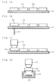
- FIGS. 5A to 5D are diagrams showing a process that is in accordance with a manufacturing method for a semiconductor wafer according to the present invention.
- a semi-finished product which has been manufactured in accordance with the above described Embodiment 1 and where a number of pieces of glass 2a have been made to adhere to the second adhesive sheet 4 is prepared (FIG. 5A).
- an adhesive sheet of which the adhesiveness is lowered through irradiation with light for example, irradiation with ultraviolet rays
- the second adhesive sheet 4 it is preferable to lower the adhesiveness of the second adhesive sheet 4 in advance through irradiation with light, in order to make the process for peeling pieces of glass 2a in the below described step easy.
- the rear surface portion of the second adhesive sheet 4 that corresponds to a piece of glass 2a that is the object of peeling is pushed upward by a pin 11, so as to gain the state where piece of glass 2a has been partially peeled from the second adhesive sheet 4 (FIG. 5B), and after that, piece of glass 2a is attracted through suction to a suction unit 12, and thus, piece of glass 2a is peeled from the second adhesive sheet 4 (FIG. 5C).
- the suction unit 12 that has attracted piece of glass 2a through suction is moved to a position above a semiconductor wafer 14 on the surface of which a number of adhesive layers 13 have been formed in a pattern, and piece of glass 2a is positioned so that it is made to adhere to the semiconductor wafer 14 via an adhesive layer 13, and after that, the suction of the suction unit 12 is released, and piece of glass 2a is made to adhere to the wafer (FIG. 5D).
- This operation is repeated, and thereby, the semiconductor wafer 14 to which a number of base pieces (pieces of glass 2a, in the present example) are made to adhere is manufactured in such a manner as to correspond to Claim 5.
- a light receiving portion having a micro lens is formed on the surface, providing a configuration where incident light is condensed on the light receiving element of each pixel.
- FIGS. 6A to 6E are diagrams showing an example of a process that is in accordance with a manufacturing method for a semiconductor device according to the present invention.
- the process of FIGS. 6A to 6D is similar to the process of FIGS. 5A to 5D of Embodiment 3, and therefore, the same numbers are attached to parts that are the same, and the descriptions thereof are omitted.
- the semiconductor wafer 14 that has been manufactured in the process of FIGS. 6A to 6D is cut along dividing lines 14a using a dicing unit or the like, and thereby, a semiconductor device (solid state imaging device 15, in the present example) to which a base piece (a piece of glass 2a, in the present example) is made to adhere is manufactured in such a manner as to correspond to Claim 6 (FIG. 6E).
- a semiconductor device solid state imaging device 15, in the present example
- a base piece a piece of glass 2a, in the present example
- a semiconductor device may be any type of semiconductor device where a lid is formed of a piece of glass, such as a solid state imaging device, including a CCD and a CMOS imager, or a semiconductor memory device, including an EPROM.
- a solid state imaging device including a CCD and a CMOS imager
- a semiconductor memory device including an EPROM.
- FIGS. 7A to 7D are diagrams showing another example of a process that is in accordance with a manufacturing method for a semiconductor device according of the present invention.
- the process of FIGS. 7A to 7C is similar to the process of FIGS. 5A to 5C of Embodiment 3, and therefore, the same numbers are attached to parts that are the same, and the descriptions thereof are omitted.
- the suction unit 12 that has attracted a piece of glass 2a through suction is shifted to a position above a case member 22 that contains a semiconductor element 21 having a light receiving portion, and piece of glass 2a is positioned so that it is made to adhere to the case member 22 via an adhesive layer 23, and after that, piece of glass 2a is made to adhere with suction of the suction unit 12 released (FIG. 7D).
- a semiconductor device where a base piece (a piece of glass 2a, in the present example) is made to adhere to the case member 22 that contains the semiconductor element 21 is manufactured in such a manner as to correspond to claim 7.
- Embodiments 3 to 5 cases where a piece of glass 2a that has been manufactured in accordance with Embodiment 1 is utilized are described, a semiconductor wafer or a semiconductor device can, of course, be manufactured in the same manner in the case where a piece of glass 2a with infrared ray blocking film 6 that has been manufactured in accordance with Embodiment 2 is utilized.
- the second adhesive sheet 4 shown in FIGS. 5 to 7 is replaced with the third adhesive sheet 7, and the infrared ray blocking film 6 is placed above a piece of glass 2a as shown in FIGS. 5 to 7.
- the surface on which the infrared ray blocking film 6 is placed can be positioned on the far side of the semiconductor wafer 14 without flipping pieces of glass 2a, and therefore, when this is applied to a solid state imaging device, the occurrence of defects caused by debris that may be mixed or attached to the infrared ray blocking film 6 can be easily reduced.
- glass is utilized as a base in the above described examples, it is possible to use a semiconductor base, such as a silicon base, in addition to glass, and the present invention can be applied to such cases in the same manner.
- a silicon wafer where a functional element has been formed and to which a piece of silicon for a protective cap is made to adhere can be cited as an example where the present invention is applied to a semiconductor wafer that uses a semiconductor base, such as a silicon base.
- a cut part of such a silicon wafer to which a piece of silicon for a protective cap has been made to adhere can be cited as an example where the present invention is applied to a semiconductor device that uses a semiconductor base, such as a silicon base.
Landscapes
- Dicing (AREA)
- Container, Conveyance, Adherence, Positioning, Of Wafer (AREA)
- Solid State Image Pick-Up Elements (AREA)
- Semiconductor Memories (AREA)
Abstract
Description
Claims (7)
- A manufacturing method for a base piece made to adhere to an adhesive sheet, characterized by comprising the steps of:cutting a base (2) that is made to adhere to a first adhesive sheet (1) into a number of base pieces (2a); andmaking a second adhesive sheet (4) adhere to the surfaces of said base pieces (2a) on the side opposite to the surfaces which are made to adhere to said first adhesive sheet (1).
- A manufacturing method for a base piece made to adhere to an adhesive sheet, characterized by comprising the steps of:cutting a base (2) that is made to adhere to a first adhesive sheet (1) into a number of base pieces (2a);making a second adhesive sheet (4) adhere to the surfaces of said base pieces (2a) on the side opposite to the surfaces which are made to adhere to said first adhesive sheet (1); andpeeling said first adhesive sheet (1) from said base pieces (2a).
- The manufacturing method for a base piece made to adhere to an adhesive sheet according to Claim 2, wherein
a film (6) has been formed on the surface of said base (2) on the side opposite to the surface which is made to adhere to said first adhesive sheet (1), and after said first adhesive sheet (1) is peeled, a third adhesive sheet (7) is made to adhere to the surfaces of said base pieces (2a) to which said first adhesive sheet (1) has been made to adhere. - The manufacturing method for a base piece made to adhere to an adhesive sheet according to Claim 2, wherein
a film (6) has been formed on the surface of said base (2) on the side opposite to the surface which is made to adhere to said first adhesive sheet (1), and after said first adhesive sheet (1) is peeled, a third adhesive sheet (7) is made to adhere to the surfaces of said base pieces (2a) to which said first adhesive sheet (1) has been made to adhere and said second adhesive sheet (4) is peeled from said base pieces (2a). - A manufacturing method for a semiconductor wafer, characterized by comprising the steps of:cutting a base (2) that is made to adhere to a first adhesive sheet (1) into a number of base pieces (2a);making a second adhesive sheet (4) adhere to the surfaces of said base pieces (2a) on the side opposite to the surfaces which are made to adhere to said first adhesive sheet (1);peeling said first adhesive sheet (1) from said base pieces (2a); andpeeling said base pieces (2a) from said second adhesive sheet (4) and making said base pieces (2a) adhere to a semiconductor wafer (14).
- A manufacturing method for a semiconductor device, characterized by comprising the steps of:cutting a base (2) that is made to adhere to a first adhesive sheet (1) into a number of base pieces (2a);making a second adhesive sheet (4) adhere to the surfaces of said base pieces (2a) on the side opposite to the surfaces which are made to adhere to said first adhesive sheet (1);peeling said first adhesive sheet (1) from said base pieces (2a);peeling said base pieces (2a) from said second adhesive sheet (4) and making said base pieces (2a) adhere to a semiconductor wafer (14); andcutting the semiconductor wafer (14) into pieces.
- A manufacturing method for a semiconductor wafer, characterized by comprising the steps of:cutting a base (2) that is made to adhere to a first adhesive sheet (1) into a number of base pieces (2a);making a second adhesive sheet (4) adhere to the surfaces of said base pieces (2a) on the side opposite to the surfaces which are made to adhere to said first adhesive sheet (1);peeling said first adhesive sheet (1) from said base pieces (2a); andpeeling said base piece (2a) from said second adhesive sheet (4) and making said base piece (2a) adhere to a case member (22) that contains a semiconductor element (21).
Applications Claiming Priority (2)
| Application Number | Priority Date | Filing Date | Title |
|---|---|---|---|
| JP2004174721A JP3830497B2 (en) | 2004-06-11 | 2004-06-11 | Semiconductor wafer manufacturing method and semiconductor device manufacturing method |
| JP2004174721 | 2004-06-11 |
Publications (2)
| Publication Number | Publication Date |
|---|---|
| EP1605521A2 true EP1605521A2 (en) | 2005-12-14 |
| EP1605521A3 EP1605521A3 (en) | 2007-08-08 |
Family
ID=35004301
Family Applications (1)
| Application Number | Title | Priority Date | Filing Date |
|---|---|---|---|
| EP05253596A Withdrawn EP1605521A3 (en) | 2004-06-11 | 2005-06-10 | Manufacturing method for a base piece made to adhere to an adhesive sheet, for a semiconductor wafer and for a semiconductor device |
Country Status (6)
| Country | Link |
|---|---|
| US (1) | US7438780B2 (en) |
| EP (1) | EP1605521A3 (en) |
| JP (1) | JP3830497B2 (en) |
| KR (2) | KR100714778B1 (en) |
| CN (1) | CN100501910C (en) |
| TW (1) | TWI274405B (en) |
Families Citing this family (2)
| Publication number | Priority date | Publication date | Assignee | Title |
|---|---|---|---|---|
| TWI549268B (en) * | 2013-02-27 | 2016-09-11 | 精材科技股份有限公司 | Wafer packaging method |
| CN107738135A (en) * | 2017-11-24 | 2018-02-27 | 深圳市精品诚电子科技有限公司 | The method of machining eyeglass chip removal |
Citations (2)
| Publication number | Priority date | Publication date | Assignee | Title |
|---|---|---|---|---|
| JPH03151666A (en) | 1989-11-08 | 1991-06-27 | Nec Corp | Manufacture of solid image-pickup device |
| JPH0541461A (en) | 1991-08-02 | 1993-02-19 | Nippon Electric Glass Co Ltd | Manufacture of small glass panel with adhesive |
Family Cites Families (18)
| Publication number | Priority date | Publication date | Assignee | Title |
|---|---|---|---|---|
| USH208H (en) * | 1984-02-17 | 1987-02-03 | At&T Bell Laboratories | Packaging microminiature devices |
| IT8921420V0 (en) | 1989-07-13 | 1989-07-13 | Telettra Spa | SYSTEM AND CIRCUIT FOR THE CALCULATION OF TWO-DIMENSIONAL DISCRETE TRANSFORMED. |
| JPH0653586B2 (en) * | 1990-03-08 | 1994-07-20 | 株式会社巴川製紙所 | Method for processing cap glass for solid-state imaging device |
| JP3165192B2 (en) * | 1991-03-28 | 2001-05-14 | 株式会社東芝 | Method for manufacturing semiconductor integrated circuit device |
| US5591290A (en) * | 1995-01-23 | 1997-01-07 | Wallace Computer Services, Inc. | Method of making a laminate having variable adhesive properties |
| FR2764111A1 (en) * | 1997-06-03 | 1998-12-04 | Sgs Thomson Microelectronics | METHOD FOR MANUFACTURING SEMICONDUCTOR PACKAGES INCLUDING AN INTEGRATED CIRCUIT |
| JPH1140520A (en) * | 1997-07-23 | 1999-02-12 | Toshiba Corp | Method of dividing wafer and method of manufacturing semiconductor device |
| US6428650B1 (en) * | 1998-06-23 | 2002-08-06 | Amerasia International Technology, Inc. | Cover for an optical device and method for making same |
| JP3447602B2 (en) * | 1999-02-05 | 2003-09-16 | シャープ株式会社 | Method for manufacturing semiconductor device |
| JP3455762B2 (en) | 1999-11-11 | 2003-10-14 | カシオ計算機株式会社 | Semiconductor device and manufacturing method thereof |
| JP3906962B2 (en) * | 2000-08-31 | 2007-04-18 | リンテック株式会社 | Manufacturing method of semiconductor device |
| JP2003086540A (en) | 2001-09-07 | 2003-03-20 | Toshiba Corp | Semiconductor device manufacturing method and its manufacturing apparatus |
| JP3881888B2 (en) | 2001-12-27 | 2007-02-14 | セイコーエプソン株式会社 | Optical device manufacturing method |
| JP2003224085A (en) | 2002-01-30 | 2003-08-08 | Disco Abrasive Syst Ltd | Semiconductor chip pickup method |
| JP2004040050A (en) | 2002-07-08 | 2004-02-05 | Toshiba Corp | Semiconductor device manufacturing method and manufacturing apparatus |
| JP2004296453A (en) | 2003-02-06 | 2004-10-21 | Sharp Corp | Solid-state imaging device, semiconductor wafer, module for optical device, method for manufacturing solid-state imaging device, and method for manufacturing module for optical device |
| JP4204368B2 (en) | 2003-03-28 | 2009-01-07 | シャープ株式会社 | Optical device module and method of manufacturing optical device module |
| JP4236594B2 (en) | 2004-01-27 | 2009-03-11 | シャープ株式会社 | Optical device module and method of manufacturing optical device module |
-
2004
- 2004-06-11 JP JP2004174721A patent/JP3830497B2/en not_active Expired - Fee Related
-
2005
- 2005-06-09 TW TW094119080A patent/TWI274405B/en not_active IP Right Cessation
- 2005-06-09 KR KR1020050049158A patent/KR100714778B1/en not_active Expired - Fee Related
- 2005-06-09 US US11/149,520 patent/US7438780B2/en not_active Expired - Lifetime
- 2005-06-10 EP EP05253596A patent/EP1605521A3/en not_active Withdrawn
- 2005-06-11 CN CNB2005100896161A patent/CN100501910C/en not_active Expired - Fee Related
-
2006
- 2006-11-24 KR KR1020060117211A patent/KR100768870B1/en not_active Expired - Fee Related
Patent Citations (2)
| Publication number | Priority date | Publication date | Assignee | Title |
|---|---|---|---|---|
| JPH03151666A (en) | 1989-11-08 | 1991-06-27 | Nec Corp | Manufacture of solid image-pickup device |
| JPH0541461A (en) | 1991-08-02 | 1993-02-19 | Nippon Electric Glass Co Ltd | Manufacture of small glass panel with adhesive |
Also Published As
| Publication number | Publication date |
|---|---|
| KR100714778B1 (en) | 2007-05-04 |
| US7438780B2 (en) | 2008-10-21 |
| CN100501910C (en) | 2009-06-17 |
| JP2005353921A (en) | 2005-12-22 |
| TW200601504A (en) | 2006-01-01 |
| EP1605521A3 (en) | 2007-08-08 |
| KR100768870B1 (en) | 2007-10-19 |
| CN1716533A (en) | 2006-01-04 |
| US20050274451A1 (en) | 2005-12-15 |
| JP3830497B2 (en) | 2006-10-04 |
| TWI274405B (en) | 2007-02-21 |
| KR20060132768A (en) | 2006-12-22 |
| KR20060048298A (en) | 2006-05-18 |
Similar Documents
| Publication | Publication Date | Title |
|---|---|---|
| KR100451950B1 (en) | Sawing method for image sensor device wafer | |
| JP5091066B2 (en) | Method for manufacturing solid-state imaging device | |
| US20090298219A1 (en) | Method for Manufacturing Solid-State Image Pickup Device Module | |
| TWI591753B (en) | Use of a vacuum tip for holding a wafer or stack of wafers | |
| US20080086858A1 (en) | Method and apparatus of fabricating a semiconductor device by back grinding and dicing | |
| US20060220183A1 (en) | Semiconductor wafer having multiple semiconductor elements and method for dicing the same | |
| US20150318326A1 (en) | Wafer-Level Bonding Method For Camera Fabrication | |
| JP2014029921A (en) | Semiconductor device processing method and semiconductor substrate processed article | |
| JP2009533867A (en) | Method of installing a protective cover on an image pickup apparatus and apparatus manufactured by the method | |
| US20080303129A1 (en) | Patterned contact sheet to protect critical surfaces in manufacturing processes | |
| JPH09330940A (en) | Method for manufacturing semiconductor device | |
| US7438780B2 (en) | Manufacturing method for base piece made to adhere to adhesive sheet, manufacturing method for semiconductor wafer and manufacturing method for semiconductor device | |
| US9419050B2 (en) | Manufacturing method of semiconductor structure with protein tape | |
| CN104992955A (en) | Backside-illuminated image sensor wafer level packaging process and packaging structure | |
| JP2006222142A (en) | Method for manufacturing semiconductor element | |
| JP4173778B2 (en) | Method for manufacturing element substrate | |
| JP4763251B2 (en) | Imaging apparatus, manufacturing method thereof, and camera module | |
| TW201034060A (en) | Techniques for glass attachment in an image sensor package | |
| JP2006196823A (en) | Method of manufacturing semiconductor device | |
| CN104009052B (en) | Wafer packaging method | |
| JP2006313921A (en) | Method for manufacturing substrate piece affixed to adhesive sheet | |
| KR101027844B1 (en) | Manufacturing Method of Image Sensor Including Wafer Back Polishing | |
| KR100720459B1 (en) | Manufacturing Method of Image Sensor | |
| JPH11126892A (en) | Solid-state image-pickup device and manufacture thereof | |
| US9023676B2 (en) | Wafer packaging method |
Legal Events
| Date | Code | Title | Description |
|---|---|---|---|
| PUAI | Public reference made under article 153(3) epc to a published international application that has entered the european phase |
Free format text: ORIGINAL CODE: 0009012 |
|
| AK | Designated contracting states |
Kind code of ref document: A2 Designated state(s): AT BE BG CH CY CZ DE DK EE ES FI FR GB GR HU IE IS IT LI LT LU MC NL PL PT RO SE SI SK TR |
|
| AX | Request for extension of the european patent |
Extension state: AL BA HR LV MK YU |
|
| PUAL | Search report despatched |
Free format text: ORIGINAL CODE: 0009013 |
|
| AK | Designated contracting states |
Kind code of ref document: A3 Designated state(s): AT BE BG CH CY CZ DE DK EE ES FI FR GB GR HU IE IS IT LI LT LU MC NL PL PT RO SE SI SK TR |
|
| AX | Request for extension of the european patent |
Extension state: AL BA HR LV MK YU |
|
| 17P | Request for examination filed |
Effective date: 20070807 |
|
| AKX | Designation fees paid |
Designated state(s): DE FR GB |
|
| 17Q | First examination report despatched |
Effective date: 20080520 |
|
| STAA | Information on the status of an ep patent application or granted ep patent |
Free format text: STATUS: THE APPLICATION IS DEEMED TO BE WITHDRAWN |
|
| 18D | Application deemed to be withdrawn |
Effective date: 20081001 |